WO2011007527A1 - Substrat stratifié métallique destiné à être utilisé en tant que matériau de fil d'oxyde supraconducteur, et son procédé de fabrication - Google Patents
Substrat stratifié métallique destiné à être utilisé en tant que matériau de fil d'oxyde supraconducteur, et son procédé de fabrication Download PDFInfo
- Publication number
- WO2011007527A1 WO2011007527A1 PCT/JP2010/004460 JP2010004460W WO2011007527A1 WO 2011007527 A1 WO2011007527 A1 WO 2011007527A1 JP 2010004460 W JP2010004460 W JP 2010004460W WO 2011007527 A1 WO2011007527 A1 WO 2011007527A1
- Authority
- WO
- WIPO (PCT)
- Prior art keywords
- copper
- copper foil
- oxide superconducting
- crystal orientation
- metal plate
- Prior art date
Links
Images


Classifications
-
- H—ELECTRICITY
- H01—ELECTRIC ELEMENTS
- H01B—CABLES; CONDUCTORS; INSULATORS; SELECTION OF MATERIALS FOR THEIR CONDUCTIVE, INSULATING OR DIELECTRIC PROPERTIES
- H01B12/00—Superconductive or hyperconductive conductors, cables, or transmission lines
- H01B12/02—Superconductive or hyperconductive conductors, cables, or transmission lines characterised by their form
- H01B12/06—Films or wires on bases or cores
-
- B—PERFORMING OPERATIONS; TRANSPORTING
- B32—LAYERED PRODUCTS
- B32B—LAYERED PRODUCTS, i.e. PRODUCTS BUILT-UP OF STRATA OF FLAT OR NON-FLAT, e.g. CELLULAR OR HONEYCOMB, FORM
- B32B15/00—Layered products comprising a layer of metal
- B32B15/01—Layered products comprising a layer of metal all layers being exclusively metallic
- B32B15/013—Layered products comprising a layer of metal all layers being exclusively metallic one layer being formed of an iron alloy or steel, another layer being formed of a metal other than iron or aluminium
- B32B15/015—Layered products comprising a layer of metal all layers being exclusively metallic one layer being formed of an iron alloy or steel, another layer being formed of a metal other than iron or aluminium the said other metal being copper or nickel or an alloy thereof
-
- B—PERFORMING OPERATIONS; TRANSPORTING
- B32—LAYERED PRODUCTS
- B32B—LAYERED PRODUCTS, i.e. PRODUCTS BUILT-UP OF STRATA OF FLAT OR NON-FLAT, e.g. CELLULAR OR HONEYCOMB, FORM
- B32B15/00—Layered products comprising a layer of metal
- B32B15/04—Layered products comprising a layer of metal comprising metal as the main or only constituent of a layer, which is next to another layer of the same or of a different material
-
- B—PERFORMING OPERATIONS; TRANSPORTING
- B32—LAYERED PRODUCTS
- B32B—LAYERED PRODUCTS, i.e. PRODUCTS BUILT-UP OF STRATA OF FLAT OR NON-FLAT, e.g. CELLULAR OR HONEYCOMB, FORM
- B32B15/00—Layered products comprising a layer of metal
- B32B15/20—Layered products comprising a layer of metal comprising aluminium or copper
-
- C—CHEMISTRY; METALLURGY
- C22—METALLURGY; FERROUS OR NON-FERROUS ALLOYS; TREATMENT OF ALLOYS OR NON-FERROUS METALS
- C22C—ALLOYS
- C22C9/00—Alloys based on copper
-
- C—CHEMISTRY; METALLURGY
- C22—METALLURGY; FERROUS OR NON-FERROUS ALLOYS; TREATMENT OF ALLOYS OR NON-FERROUS METALS
- C22F—CHANGING THE PHYSICAL STRUCTURE OF NON-FERROUS METALS AND NON-FERROUS ALLOYS
- C22F1/00—Changing the physical structure of non-ferrous metals or alloys by heat treatment or by hot or cold working
- C22F1/08—Changing the physical structure of non-ferrous metals or alloys by heat treatment or by hot or cold working of copper or alloys based thereon
-
- H—ELECTRICITY
- H01—ELECTRIC ELEMENTS
- H01B—CABLES; CONDUCTORS; INSULATORS; SELECTION OF MATERIALS FOR THEIR CONDUCTIVE, INSULATING OR DIELECTRIC PROPERTIES
- H01B13/00—Apparatus or processes specially adapted for manufacturing conductors or cables
-
- H—ELECTRICITY
- H10—SEMICONDUCTOR DEVICES; ELECTRIC SOLID-STATE DEVICES NOT OTHERWISE PROVIDED FOR
- H10N—ELECTRIC SOLID-STATE DEVICES NOT OTHERWISE PROVIDED FOR
- H10N60/00—Superconducting devices
- H10N60/01—Manufacture or treatment
- H10N60/0268—Manufacture or treatment of devices comprising copper oxide
- H10N60/0296—Processes for depositing or forming superconductor layers
- H10N60/0576—Processes for depositing or forming superconductor layers characterised by the substrate
-
- Y—GENERAL TAGGING OF NEW TECHNOLOGICAL DEVELOPMENTS; GENERAL TAGGING OF CROSS-SECTIONAL TECHNOLOGIES SPANNING OVER SEVERAL SECTIONS OF THE IPC; TECHNICAL SUBJECTS COVERED BY FORMER USPC CROSS-REFERENCE ART COLLECTIONS [XRACs] AND DIGESTS
- Y10—TECHNICAL SUBJECTS COVERED BY FORMER USPC
- Y10T—TECHNICAL SUBJECTS COVERED BY FORMER US CLASSIFICATION
- Y10T428/00—Stock material or miscellaneous articles
- Y10T428/12—All metal or with adjacent metals
- Y10T428/12493—Composite; i.e., plural, adjacent, spatially distinct metal components [e.g., layers, joint, etc.]
- Y10T428/12771—Transition metal-base component
- Y10T428/12861—Group VIII or IB metal-base component
- Y10T428/12903—Cu-base component
Definitions
- the present invention relates to a method for producing a metal laminated substrate for oxide superconducting wire and a metal laminated substrate for oxide superconducting wire.
- an intermediate layer (CeO 2 or zirconia-added yttrium oxide (YSZ)) and a superconducting film (RE123 film: RE: Y, Gd, Ho on a metal substrate are provided. Etc.) need to be formed.
- oxide film deposition methods include ion-assisted beam deposition (IBAD) and RABITS, in which an oxide is deposited on a previously crystallized metal substrate. ing.
- Oxide superconducting wire manufactured by the RABITS method is advantageous when considering future production efficiency such as film formation speed, but it is important to keep the metal substrate highly crystallized in order to improve superconducting properties. is there.
- a substrate is disclosed in which copper is laminated on a stainless steel substrate, copper is highly crystallized, and a nickel intermediate layer is laminated thereon (see, for example, Patent Document 1).
- Patent Document 1 has a problem that the orientation of copper laminated on the stainless steel substrate is not sufficient, and scratches and grooves may be generated on the surface.
- Patent Document 2 employs a means for crystallizing copper and then laminating it on a stainless steel substrate by cold rolling, the crystal-oriented copper is rolled. In some cases, the copper orientation is lowered or the copper surface is scratched or grooved. For this reason, there is a problem that the orientation of the nickel layer, the superconducting layer, etc. laminated thereon is lowered, and the characteristics of the superconductor may be lowered.
- the present invention provides a metal laminated substrate for an oxide superconducting wire and a method for producing the same, which can solve such problems and highly orient copper and prevent the formation of scratches and grooves on the surface.
- another object of the present invention is to allow copper to be laminated on a substrate with less change in the reduction state of copper, and to highly orient copper when orienting copper that has been reduced by subsequent heat treatment. It is to provide a metal laminated substrate for an oxide superconducting wire and a method for producing the same.
- another object of the present invention is to provide a metal laminated substrate for oxide superconducting wire and a method for producing the same, which can realize the adhesion required for the substrate simultaneously with the high orientation of copper by controlling the pressing conditions. It is.
- the manufacturing method of the metal laminated substrate for oxide superconducting wire of the present invention includes: A step of removing the adsorbate on the surface by sputter etching the surface of the copper foil in a state in which the copper foil rolled at a rolling reduction of 90% or more is kept below the crystal orientation temperature; A step of sputter etching the surface of the non-magnetic metal plate to remove the adsorbate on the surface; Bonding the copper foil and the metal plate with a pressure of 300 MPa to 1500 MPa by a rolling roll; Heating the bonded laminate to a temperature equal to or higher than the crystal orientation temperature of copper to crystallize the copper; And a step of coating a protective layer on the copper side surface of the laminate.
- the method for producing a metal laminated substrate for an oxide superconducting wire according to the present invention is characterized in that, in the above (1), the sputter etching of the copper foil is performed at a temperature of less than 150 ° C. (3)
- the step of sputter-etching the nonmagnetic metal plate is less than the crystal orientation temperature of the copper foil. In this state, the surface of the substrate is sputter-etched to remove the adsorbate on the surface.
- the metal laminated substrate for oxide superconducting wire of the present invention is A non-magnetic metal plate, Having a copper layer on the metal plate; Further, a metal laminated substrate for oxide superconducting wire having a protective layer on the copper layer, The C-axis crystal orientation of the protective layer is 99% or more, And the adhesive strength of the said copper layer and the said metal plate is 0.1 N / cm or more by 180 degree peel strength, It is characterized by the above-mentioned.
- the heat treatment is performed to crystallize the copper, so that copper is highly oriented compared to the prior art and prevents the formation of scratches and grooves on the surface. It becomes possible to do. Furthermore, by adhering the surface of the copper foil and non-magnetic metal plate below the crystal orientation temperature of copper, the adsorbate remains in the same crystal state as the copper foil before etching without recrystallizing the copper foil. By controlling the reduction conditions, it is possible to ensure a sufficient adhesion while maintaining the crystal state of the copper foil at the same level as that of the copper foil before etching. By controlling the bonding conditions in this manner, the crystal state can be maintained at the same level as that of the copper foil before etching even after lamination, so that the copper can be highly crystallized by subsequent heat treatment.
- FIG. 1 shows a schematic view of a surface activated bonding apparatus used in the present invention. It is a graph which shows the relationship between the crystal orientation rate of the 200 ppmAg addition rolling copper foil (200) surface used with the manufacturing method of this invention, and heat processing holding time.
- the surface of the copper foil is sputter-etched with the copper foil rolled at a rolling reduction of 90% or less kept below the crystal orientation temperature.
- Remove the adsorbed material on the surface Sputter etching the surface of the non-magnetic metal plate to remove the adsorbed material on the surface,
- a copper foil and a metal plate are joined with a rolling roll at a pressure of 300 MPa to 1500 MPa, and the joined laminate is heated to a temperature equal to or higher than the crystal orientation temperature of copper to crystallize copper, and on the copper side surface of the laminate
- the protective layer is coated on.
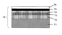
- FIG. 1 is a schematic cross-sectional view showing the configuration of a metal laminated substrate 5A for an oxide superconducting wire obtained by the production method of the present invention.
- a metal laminated substrate 5A for an oxide superconducting wire includes a nonmagnetic metal plate T1 serving as a metal substrate, a copper foil T2 (copper layer) laminated on the nonmagnetic metal plate T1, and a copper foil T2.
- the nonmagnetic metal plate T1 is used for the role of a copper foil reinforcing plate, and has a higher strength than a nonmagnetic (antiferromagnetic or paramagnetic) copper foil under 77K where an oxide superconducting wire is used. Can be mentioned. Further, the nonmagnetic metal plate T1 is preferably a softened state, that is, a so-called annealed material (O material). The reason for this is to use a copper foil that has been cold-rolled and hardened at a high pressure reduction rate to secure the contact area of the above-mentioned bonding interface under a low pressure as much as possible, and to reduce warping after rolling. It is.
- the nonmagnetic metal plate T1 include, for example, an annealed material of a stainless steel plate such as SUS316L.
- the thickness is preferably 0.05 mm or more and 0.2 mm or less. The reason why the thickness is 0.05 mm or more is to ensure the strength of the nonmagnetic metal plate T1, and the reason why the thickness is 0.2 mm or less is to ensure workability when processing the superconductor.
- the copper foil T2 it is preferable to use a so-called full-hard material made of copper or a copper alloy that is cold-rolled at a reduction rate of 90% or more (in the present specification, both may be referred to as a copper foil).
- the reason why the rolling reduction is 90% or more is that Cu may not be oriented in a heat treatment performed later in a copper foil having a rolling reduction of less than 90%.
- the thickness of the copper foil T2 is preferably 7 ⁇ m or more and 50 ⁇ m or less from the viewpoint of strength and workability.
- the composition of copper foil adds 100 ppm or more and 1% or less in total of additive elements, such as Ag, Sn, Zn, Zr, O, and N, in Cu base.
- additive elements such as Ag, Sn, Zn, Zr, O, and N
- the total amount of these additive elements exceeds 1%, oxides and the like are formed in the Cu matrix, which adversely affects the surface cleanliness.
- the crystal orientation may be deteriorated.
- the effect of Ag addition is particularly effective for improving crystal orientation, and the amount of Ag added is preferably 200 ppm to 300 ppm.
- the metal laminated substrate manufactured by the manufacturing method of this embodiment is for oxide superconducting wires, and an oxide intermediate layer such as CeO 2 or YSZ is formed in a high-temperature oxidizing atmosphere at 600 ° C. or higher in a later step. Is done. Therefore, coating the oxide intermediate layer directly on the copper surface may make it difficult to ensure uniform adhesion due to the surface oxidation of the copper. After the heat treatment, Ni on the copper foil surface may be difficult. It is preferred to coat the layer.
- the Ni layer coating method may be any epitaxial growth method so as to inherit the high biaxial crystal orientation of the copper foil.
- the electrolytic Ni plating method is preferable. Any electrolytic Ni plating bath may be used as long as it is matte plating or semi-gloss plating such as a normal watt bath, chloride bath or sulfamic acid bath.
- the thickness of the Ni plating layer should be as thin as possible.
- the thickness should be set to 1 ⁇ m to 3 ⁇ m. preferable.
- the Ni film includes a Ni alloy film.
- the metal laminated substrate for oxide superconducting wire 5A shown in FIG. 1 is laminated by bonding the nonmagnetic metal plate T1 and the copper foil T2 with a rolling roll after washing.
- the cleaning method may be any of dry, wet, wet / dry combined use.
- a process such as sputtering with an inert gas (Ar, Ne, etc.) or etching with an ion beam in a vacuum.
- a wet type after dipping into a general sulfuric acid pickling or alkaline cleaning solution, it is washed with water and dried after a degreasing treatment by electrolysis.
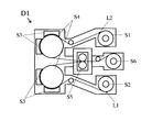
- the vacuum clad continuous device D1 as shown in FIG. 5 continuously performs dry etching before the rolling by the rolling roll, A method of removing the oxide film layer is preferably employed.
- a nonmagnetic metal plate L1 and a copper foil L2 are prepared as long coils having a width of 150 mm to 600 mm, and are installed in the recoiler parts S1 and S2 of the surface activated bonding apparatus D1.
- the non-magnetic metal plate L1 and the copper foil L2 conveyed from the recoiler parts S1 and S2 are continuously conveyed to the surface activation treatment step, and after the two surfaces to be joined are activated in advance, cold welding is performed. To do.
- the nonmagnetic metal plate L1 and the copper foil L2 having the joint surface are each grounded and grounded as one electrode A (S3), and the other electrode B (S4) that is insulated and supported.
- Glow discharge is generated by applying an alternating current of 1 to 50 MHz, and the area of the electrode exposed in the plasma generated by the glow discharge is sputter-etched so that it is 1/3 or less of the area of the electrode B.
- the inert gas argon, neon, xenon, krypton, or a mixed gas containing at least one of these can be used.
- the surface to be joined is sputtered with an inert gas to remove the surface adsorption layer and the surface oxide film, and the surface to be joined is activated by sputtering the nonmagnetic metal plate L1 and the copper foil L2.
- the electrode A (S3) takes the form of a cooling roll to prevent the temperature of each conveying material from rising.
- the adsorbate on the bonding surface is completely removed, but the surface oxide layer does not have to be completely removed. Even if an oxide layer remains on the entire surface, it is possible to ensure the bondability between the metal plate and the copper foil by increasing the rolling reduction in the bonding process and exposing the substrate by friction at the bonding surface. is there.
- the recrystallization start temperature of the copper foil is around 150 ° C.
- the copper foil temperature rises to 150 ° C. or higher during the sputter etching process the copper foil recrystallizes and the copper foil is crystallized before bonding. It will be.
- strain introduced into the copper foil and the biaxial crystal orientation of the copper foil is deteriorated.
- the strain introduced by rolling is slight, even if the subsequent heat treatment is performed, the crystal orientation cannot be highly achieved. For this reason, it is necessary to keep the temperature of the copper foil below 150 ° C. in the sputter etching process.
- the metal plate is processed at a high plasma output or the temperature of the metal plate is increased to 150 ° C. or more over time, the metal plate is heated depending on the vacuum conditions, The copper foil temperature increases due to contact with the copper foil, and recrystallization of the copper foil occurs simultaneously with rolling, which may deteriorate the biaxial crystal orientation. For this reason, it is desirable to keep the temperature of the metal plate below 150 ° C. even in the sputter etching process of the nonmagnetic metal plate. Preferably, it is kept at room temperature to 100 ° C.
- the degree of vacuum at this time is preferably higher in order to prevent re-adsorbed substances on the surface, but it may be 10 ⁇ 5 Pa or more and 10 ⁇ 2 Pa or less.
- pressure bonding is performed in a non-oxidizing atmosphere, for example, an inert gas atmosphere such as Ar. Is also preferable.
- the pressing by the rolling roll is preferably performed in order to secure a close contact area at the bonding interface, and to peel off a part of the surface oxide film layer by friction occurring at the bonding interface during the reduction to expose the substrate, and to apply 300 MPa or more.
- the metal plate is a strength reinforcing material
- the copper foil to be bonded is also full hard, and both materials are hard. Therefore, pressurization at 600 MPa to 1.5 GPa is preferable.
- the pressurization may be applied more than this, and it has been confirmed that the crystal orientation does not deteriorate after the subsequent heat treatment up to a reduction rate of 30%. However, if further processing is applied, cracks are generated on the surface of the copper foil, and the crystal orientation of the copper foil after rolling and heat treatment becomes poor.
- the laminated body After joining the copper foil and the nonmagnetic metal plate by the rolling roll, the laminated body is heat-treated in order to crystallize the copper foil, and after the copper foil T2 is biaxially crystallized, the copper foil T2 side surface is protected. Layer T3 is formed.
- the heat treatment temperature may be 150 ° C. or more as long as the copper foil and the nonmagnetic metal plate are sufficiently adhered.
- an annealed material of a stainless steel plate is used as the nonmagnetic metal plate, the strength hardly changes by heat treatment. Even when a rolled material that is not annealed is used, even if the heat treatment time is about 1 to 10 minutes even at a high temperature of 600 ° C. or higher, there is no significant decrease in strength, and the role as a strength reinforcing material is sufficiently fulfilled.
- Table 1 shows the results when the high pressure lower copper foil added with 200 ppm of Ag having a width of 200 mm and a thickness of 18 ⁇ m and SUS316L (annealed material) having a thickness of 100 ⁇ m were passed through using a surface activated bonding apparatus as shown in FIG.
- the relationship between Ar sputter etching time and the pressurization with the rolling roll in the subsequent joining process and the adhesion strength (180 degree peel strength) of the joined material is shown.
- the plasma output was 200 W under 0.1 Pa
- the plate passing speed was changed
- the sputter irradiation time to the bonding surface was changed.
- the joining was performed by changing the pressure on the rolling roll from 100 MPa to 1500 MPa.
- the sample after bonding had a (200) plane C-axis crystal orientation measured by ⁇ / 2 ⁇ measurement by X-ray diffraction. It was measured.
- the (200) plane crystal orientation ratio up to 30% was regarded as no occurrence of crystal orientation (recrystallization).
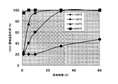
- FIG. 6 shows the relationship between the crystal orientation rate and the heat treatment holding time of the rolled copper foil (200) surface with 200 ppm Ag added. After the heat treatment, the crystal orientation ratio was measured by ⁇ / 2 ⁇ using an X-ray diffractometer, and the C-axis orientation of the (200) plane was measured.
- the C-axis orientation is the X-ray diffraction intensity (200) plane of the total (represented as ⁇ I (hkl)) of the (111) plane, (200) plane, (220) plane, and (311) plane (represented as ⁇ I (hkl)).
- (200) plane crystal orientation ratio I (200) / ⁇ I ⁇ 100 (%).
- the (200) plane is about 20% to 30% in the rolled state without heat treatment. From FIG. 6, it can be seen that there is no change in the crystal orientation when the heat treatment is lower than 150 ° C. for about 1 minute. However, when the temperature is maintained further, particularly at a temperature of 150 ° C. or higher, the recrystallization of copper proceeds rapidly and the (200) plane increases rapidly.
- the sputter etching time is increased to 60 seconds and 300 seconds, and when the adsorbate and the surface oxide layer are removed, the adhesion strength increases, but during sputter etching. Then, copper recrystallizes and crystal orientation occurs.
- the thicknesses of the oxide films of the copper foil and the stainless steel plate used in this experiment were 5 nm and 10 nm, respectively, as measured by an Auger electron microscope before bonding.
- the Ar sputtering rate at an RF output of 200 W was obtained by measuring the sputtering rate of copper and stainless steel based on the sputtering rate by standard measurement of sputtering of Si. For example, in order to completely remove the oxide film on the stainless steel surface, it took 5 minutes at an RF output of 200 W in the sputtering apparatus in the present bonding apparatus.
- the surface state described in the remarks column in Table 1 is assumed to be the surface state after sputter etching.
- Table 2 shows the degree of (200) plane crystal orientation on the copper foil side after the Cu / SUS316L laminated substrate shown in Example 1 is held at 150 ° C. to 950 ° C. for 5 minutes to 4 hours in a non-oxidizing atmosphere, and heat treatment Later, the (200) plane crystal orientation degree and the C-axis crystal orientation ratio of the protective layer (Ni layer) when 1 ⁇ m thick Ni plating is applied to the copper foil surface side are shown together with comparative experimental examples.
- the Ni plating was performed using a general Watt bath at a current density of 4 A / dm 2 , a bath temperature of 60 ° C., and a pH of 3.
- ⁇ of copper when heat-treating the metal laminated substrate of Comparative Experimental Example 1-5 (sputtering time 120 seconds, pressure 300 MPa) shown in Example 1 is also shown.
- This sample has crystallized once before bonding, and after that, since 300 MPa is applied in the bonding process, strain is introduced. Therefore, the biaxial crystal orientation is deteriorated even after the heat treatment, and ⁇ shows a value of 6 ° or more. Further, when this sample is heat-treated at a relatively high temperature of 850 ° C., secondary recrystallization occurs due to the introduction of strain, and the crystal orientation is greatly lost.
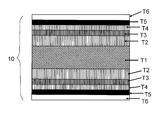
- FIG. 2 is a schematic cross-sectional view showing a configuration of an oxide superconducting wire 10A in which an intermediate layer T4, an oxide superconductor layer T5, and a protective film T6 are sequentially laminated on the metal laminated substrate 5A for oxide superconducting wire shown in FIG. It is.
- the oxide superconducting wire 10A is formed by epitaxially depositing an intermediate layer such as CeO 2 , YSZ, SrTiO 3 , or MgO on the protective layer T3 using a sputtering method or the like, and forming a superconductor layer such as a Y123-based thin film using a laser ablation method or the like. It is manufactured by forming a film and laminating Ag, Cu or the like as a protective film on the superconductor layer.
- FIG. 3 shows a metal laminate for an oxide superconducting wire.
- a copper foil T2 is applied to both surfaces of a nonmagnetic metal plate T1 by surface activation bonding, and after heat treatment, a Ni layer protective layer T3 is applied to both surfaces.
- FIG. 4 is a schematic cross-sectional view showing a configuration of an oxide superconducting wire 10B using the metal laminated plate for oxide superconducting wire shown in FIG.
- the heat treatment is performed to crystallize the copper, so that copper is highly oriented compared to the prior art and prevents the formation of scratches and grooves on the surface. It is possible to stack copper on the substrate with less change in copper reduction than in the prior art by sputter etching copper while maintaining the temperature below the crystal start temperature of copper, and then heating Compared with the prior art, copper can be highly oriented when orienting copper that has been reduced by processing. Furthermore, since copper is sputter-etched at a temperature lower than the crystal start temperature of copper, there is a high possibility that an oxide layer will remain on the copper surface. With conventional technology, the adhesion between copper and the substrate tends to decrease. In the invention, by controlling the pressing conditions, the adhesion required for the substrate can be realized simultaneously with the high orientation of copper, and the industrial applicability is extremely high.
Landscapes
- Chemical & Material Sciences (AREA)
- Engineering & Computer Science (AREA)
- Materials Engineering (AREA)
- Mechanical Engineering (AREA)
- Metallurgy (AREA)
- Organic Chemistry (AREA)
- Manufacturing & Machinery (AREA)
- Thermal Sciences (AREA)
- Crystallography & Structural Chemistry (AREA)
- Physics & Mathematics (AREA)
- Superconductors And Manufacturing Methods Therefor (AREA)
- Pressure Welding/Diffusion-Bonding (AREA)
- ing And Chemical Polishing (AREA)
Abstract
Priority Applications (6)
| Application Number | Priority Date | Filing Date | Title |
|---|---|---|---|
| US13/383,957 US8815777B2 (en) | 2009-07-17 | 2010-07-08 | Metal laminated substrate for use as an oxide superconducting wire material, and manufacturing method therefor |
| KR1020117030690A KR101680756B1 (ko) | 2009-07-17 | 2010-07-08 | 산화물 초전도 선재용 금속 적층 기판의 제조 방법 |
| CN2010800280233A CN102473486B (zh) | 2009-07-17 | 2010-07-08 | 氧化物超导线材用金属叠层基板的制造方法及氧化物超导线材用金属叠层基板 |
| IN632DEN2012 IN2012DN00632A (fr) | 2009-07-17 | 2010-07-08 | |
| EP10799591.2A EP2455949B1 (fr) | 2009-07-17 | 2010-07-08 | Substrat stratifié métallique destiné à être utilisé en tant que matériau de fil d'oxyde supraconducteur, et son procédé de fabrication |
| JP2011522708A JP5723773B2 (ja) | 2009-07-17 | 2010-07-08 | 酸化物超電導線材用金属積層基板の製造方法 |
Applications Claiming Priority (2)
| Application Number | Priority Date | Filing Date | Title |
|---|---|---|---|
| JP2009-169531 | 2009-07-17 | ||
| JP2009169531 | 2009-07-17 |
Publications (1)
| Publication Number | Publication Date |
|---|---|
| WO2011007527A1 true WO2011007527A1 (fr) | 2011-01-20 |
Family
ID=43449139
Family Applications (1)
| Application Number | Title | Priority Date | Filing Date |
|---|---|---|---|
| PCT/JP2010/004460 WO2011007527A1 (fr) | 2009-07-17 | 2010-07-08 | Substrat stratifié métallique destiné à être utilisé en tant que matériau de fil d'oxyde supraconducteur, et son procédé de fabrication |
Country Status (7)
| Country | Link |
|---|---|
| US (1) | US8815777B2 (fr) |
| EP (1) | EP2455949B1 (fr) |
| JP (1) | JP5723773B2 (fr) |
| KR (1) | KR101680756B1 (fr) |
| CN (1) | CN102473486B (fr) |
| IN (1) | IN2012DN00632A (fr) |
| WO (1) | WO2011007527A1 (fr) |
Cited By (8)
| Publication number | Priority date | Publication date | Assignee | Title |
|---|---|---|---|---|
| JP2013129853A (ja) * | 2011-11-22 | 2013-07-04 | Jx Nippon Mining & Metals Corp | 超電導膜形成用圧延銅箔 |
| JP2013129854A (ja) * | 2011-11-22 | 2013-07-04 | Jx Nippon Mining & Metals Corp | 超電導膜形成用圧延銅箔 |
| JP2013136807A (ja) * | 2011-12-28 | 2013-07-11 | Jx Nippon Mining & Metals Corp | 超電導膜形成用圧延銅箔 |
| JP2013235796A (ja) * | 2012-05-11 | 2013-11-21 | Jx Nippon Mining & Metals Corp | 超電導膜形成用圧延銅箔 |
| WO2015033727A1 (fr) | 2013-09-04 | 2015-03-12 | 東洋鋼鈑株式会社 | Substrat de matériau de fil supraconducteur, procédé de production associé et matériau de fil supraconducteur |
| KR20150067128A (ko) * | 2012-10-05 | 2015-06-17 | 도요 고한 가부시키가이샤 | 에피택셜 성장용 기판 및 그 제조 방법과 초전도 선재용 기판 |
| JPWO2015033808A1 (ja) * | 2013-09-04 | 2017-03-02 | 東洋鋼鈑株式会社 | 酸化物層の成膜方法、並びにエピタキシャル成長用積層基材及びその製造方法 |
| WO2017069255A1 (fr) * | 2015-10-23 | 2017-04-27 | 東洋鋼鈑株式会社 | Substrat pour croissance épitaxiale et son procédé de production |
Families Citing this family (6)
| Publication number | Priority date | Publication date | Assignee | Title |
|---|---|---|---|---|
| CN103718256B (zh) * | 2012-04-16 | 2016-11-16 | 古河电气工业株式会社 | 超导成膜用基材和超导线以及超导线的制造方法 |
| WO2013180443A1 (fr) * | 2012-05-29 | 2013-12-05 | 한국생산기술연구원 | Barre omnibus en fer ayant une couche de cuivre, et procédé de fabrication de cette dernière |
| CN104538543B (zh) * | 2014-12-11 | 2017-06-20 | 西部超导材料科技股份有限公司 | 一种低温超导线材用NbTi棒的制备方法 |
| WO2018181721A1 (fr) * | 2017-03-29 | 2018-10-04 | 東洋鋼鈑株式会社 | Corps plaqué par laminage |
| WO2019239574A1 (fr) * | 2018-06-15 | 2019-12-19 | 住友電気工業株式会社 | Fil supraconducteur, fil supraconducteur stratifié, bobine supraconductrice, et câble supraconducteur |
| JP2021171963A (ja) * | 2020-04-22 | 2021-11-01 | 東洋鋼鈑株式会社 | 金属積層フィルム及びその製造方法 |
Citations (4)
| Publication number | Priority date | Publication date | Assignee | Title |
|---|---|---|---|---|
| JPH113620A (ja) * | 1997-06-10 | 1999-01-06 | Furukawa Electric Co Ltd:The | 酸化物超電導線材およびその製造方法 |
| JP2006127847A (ja) | 2004-10-27 | 2006-05-18 | Sumitomo Electric Ind Ltd | 膜形成用配向基板および超電導線材 |
| JP2008266686A (ja) | 2007-04-17 | 2008-11-06 | Chubu Electric Power Co Inc | エピタキシャル薄膜形成用のクラッド配向金属基板及びその製造方法 |
| JP2010118246A (ja) * | 2008-11-12 | 2010-05-27 | Toyo Kohan Co Ltd | 酸化物超電導線材用金属積層基板の製造方法及び該基板を用いた酸化物超電導線材 |
Family Cites Families (1)
| Publication number | Priority date | Publication date | Assignee | Title |
|---|---|---|---|---|
| US7816303B2 (en) * | 2004-10-01 | 2010-10-19 | American Superconductor Corporation | Architecture for high temperature superconductor wire |
-
2010
- 2010-07-08 JP JP2011522708A patent/JP5723773B2/ja active Active
- 2010-07-08 EP EP10799591.2A patent/EP2455949B1/fr active Active
- 2010-07-08 KR KR1020117030690A patent/KR101680756B1/ko active IP Right Grant
- 2010-07-08 IN IN632DEN2012 patent/IN2012DN00632A/en unknown
- 2010-07-08 US US13/383,957 patent/US8815777B2/en active Active
- 2010-07-08 WO PCT/JP2010/004460 patent/WO2011007527A1/fr active Application Filing
- 2010-07-08 CN CN2010800280233A patent/CN102473486B/zh active Active
Patent Citations (4)
| Publication number | Priority date | Publication date | Assignee | Title |
|---|---|---|---|---|
| JPH113620A (ja) * | 1997-06-10 | 1999-01-06 | Furukawa Electric Co Ltd:The | 酸化物超電導線材およびその製造方法 |
| JP2006127847A (ja) | 2004-10-27 | 2006-05-18 | Sumitomo Electric Ind Ltd | 膜形成用配向基板および超電導線材 |
| JP2008266686A (ja) | 2007-04-17 | 2008-11-06 | Chubu Electric Power Co Inc | エピタキシャル薄膜形成用のクラッド配向金属基板及びその製造方法 |
| JP2010118246A (ja) * | 2008-11-12 | 2010-05-27 | Toyo Kohan Co Ltd | 酸化物超電導線材用金属積層基板の製造方法及び該基板を用いた酸化物超電導線材 |
Non-Patent Citations (2)
| Title |
|---|
| "practice on handling of device, measurement of films, evaluations and various applications", 1985, pages: 29 |
| See also references of EP2455949A4 |
Cited By (16)
| Publication number | Priority date | Publication date | Assignee | Title |
|---|---|---|---|---|
| JP2013129854A (ja) * | 2011-11-22 | 2013-07-04 | Jx Nippon Mining & Metals Corp | 超電導膜形成用圧延銅箔 |
| JP2013129853A (ja) * | 2011-11-22 | 2013-07-04 | Jx Nippon Mining & Metals Corp | 超電導膜形成用圧延銅箔 |
| JP2013136807A (ja) * | 2011-12-28 | 2013-07-11 | Jx Nippon Mining & Metals Corp | 超電導膜形成用圧延銅箔 |
| JP2013235796A (ja) * | 2012-05-11 | 2013-11-21 | Jx Nippon Mining & Metals Corp | 超電導膜形成用圧延銅箔 |
| JPWO2014054351A1 (ja) * | 2012-10-05 | 2016-08-25 | 東洋鋼鈑株式会社 | エピタキシャル成長用基板及びその製造方法、並びに超電導線材用基板 |
| KR101975252B1 (ko) | 2012-10-05 | 2019-05-07 | 도요 고한 가부시키가이샤 | 에피택셜 성장용 기판 및 그 제조 방법과 초전도 선재용 기판 |
| KR20150067128A (ko) * | 2012-10-05 | 2015-06-17 | 도요 고한 가부시키가이샤 | 에피택셜 성장용 기판 및 그 제조 방법과 초전도 선재용 기판 |
| WO2015033727A1 (fr) | 2013-09-04 | 2015-03-12 | 東洋鋼鈑株式会社 | Substrat de matériau de fil supraconducteur, procédé de production associé et matériau de fil supraconducteur |
| KR20160051728A (ko) * | 2013-09-04 | 2016-05-11 | 도요 고한 가부시키가이샤 | 초전도 선재용 기판 및 그 제조 방법과 초전도 선재 |
| JPWO2015033808A1 (ja) * | 2013-09-04 | 2017-03-02 | 東洋鋼鈑株式会社 | 酸化物層の成膜方法、並びにエピタキシャル成長用積層基材及びその製造方法 |
| US10115501B2 (en) | 2013-09-04 | 2018-10-30 | Toyo Kohan Co., Ltd. | Substrate for superconducting wire, method for manufacturing the same, and superconducting wire |
| JP2015050147A (ja) * | 2013-09-04 | 2015-03-16 | 東洋鋼鈑株式会社 | 超電導線材用基板及びその製造方法、並びに超電導線材 |
| KR102188566B1 (ko) * | 2013-09-04 | 2020-12-08 | 도요 고한 가부시키가이샤 | 초전도 선재용 기판 및 그 제조 방법과 초전도 선재 |
| WO2017069255A1 (fr) * | 2015-10-23 | 2017-04-27 | 東洋鋼鈑株式会社 | Substrat pour croissance épitaxiale et son procédé de production |
| JPWO2017069255A1 (ja) * | 2015-10-23 | 2018-08-09 | 東洋鋼鈑株式会社 | エピタキシャル成長用基板及びその製造方法 |
| US11524486B2 (en) | 2015-10-23 | 2022-12-13 | Toyo Kohan Co., Ltd. | Substrate for epitaxtail, growth and method for producing same |
Also Published As
| Publication number | Publication date |
|---|---|
| EP2455949A4 (fr) | 2015-04-22 |
| IN2012DN00632A (fr) | 2015-08-21 |
| EP2455949B1 (fr) | 2016-08-31 |
| US8815777B2 (en) | 2014-08-26 |
| KR20120038410A (ko) | 2012-04-23 |
| CN102473486B (zh) | 2013-07-17 |
| JPWO2011007527A1 (ja) | 2012-12-20 |
| KR101680756B1 (ko) | 2016-11-29 |
| CN102473486A (zh) | 2012-05-23 |
| JP5723773B2 (ja) | 2015-05-27 |
| EP2455949A1 (fr) | 2012-05-23 |
| US20120208703A1 (en) | 2012-08-16 |
Similar Documents
| Publication | Publication Date | Title |
|---|---|---|
| JP5723773B2 (ja) | 酸化物超電導線材用金属積層基板の製造方法 | |
| JP5517196B2 (ja) | 超電導化合物用基板及びその製造方法 | |
| JP5828014B2 (ja) | 半導体素子形成用金属積層基板の製造方法及び半導体素子形成用金属積層基板 | |
| JP5382911B2 (ja) | 酸化物超電導線材用金属積層基板の製造方法及び該基板を用いた酸化物超電導線材 | |
| KR102403087B1 (ko) | 초전도 선재용 기판 및 그 제조 방법과 초전도 선재 | |
| KR102188566B1 (ko) | 초전도 선재용 기판 및 그 제조 방법과 초전도 선재 | |
| WO2015033808A1 (fr) | Procédé de formation de couche d'oxyde, et matériau de base de stratifié pour croissance épitaxiale ainsi que procédé de fabrication de celui-ci | |
| JP5606920B2 (ja) | エピタキシャル成長膜形成用高分子積層基板およびその製造方法 | |
| JP5918920B2 (ja) | 超電導化合物用基板及びその製造方法 | |
| JP6948621B2 (ja) | エピタキシャル成長用基板及びその製造方法 |
Legal Events
| Date | Code | Title | Description |
|---|---|---|---|
| WWE | Wipo information: entry into national phase |
Ref document number: 201080028023.3 Country of ref document: CN |
|
| 121 | Ep: the epo has been informed by wipo that ep was designated in this application |
Ref document number: 10799591 Country of ref document: EP Kind code of ref document: A1 |
|
| WWE | Wipo information: entry into national phase |
Ref document number: 2011522708 Country of ref document: JP |
|
| ENP | Entry into the national phase |
Ref document number: 20117030690 Country of ref document: KR Kind code of ref document: A |
|
| NENP | Non-entry into the national phase |
Ref country code: DE |
|
| WWE | Wipo information: entry into national phase |
Ref document number: 632/DELNP/2012 Country of ref document: IN |
|
| REEP | Request for entry into the european phase |
Ref document number: 2010799591 Country of ref document: EP |
|
| WWE | Wipo information: entry into national phase |
Ref document number: 2010799591 Country of ref document: EP |
|
| WWE | Wipo information: entry into national phase |
Ref document number: 13383957 Country of ref document: US |