WO2011007527A1 - Metal laminated substrate for use as an oxide superconducting wire material, and manufacturing method therefor - Google Patents
Metal laminated substrate for use as an oxide superconducting wire material, and manufacturing method therefor Download PDFInfo
- Publication number
- WO2011007527A1 WO2011007527A1 PCT/JP2010/004460 JP2010004460W WO2011007527A1 WO 2011007527 A1 WO2011007527 A1 WO 2011007527A1 JP 2010004460 W JP2010004460 W JP 2010004460W WO 2011007527 A1 WO2011007527 A1 WO 2011007527A1
- Authority
- WO
- WIPO (PCT)
- Prior art keywords
- copper
- copper foil
- oxide superconducting
- crystal orientation
- metal plate
- Prior art date
Links
Images


Classifications
-
- H—ELECTRICITY
- H01—ELECTRIC ELEMENTS
- H01B—CABLES; CONDUCTORS; INSULATORS; SELECTION OF MATERIALS FOR THEIR CONDUCTIVE, INSULATING OR DIELECTRIC PROPERTIES
- H01B12/00—Superconductive or hyperconductive conductors, cables, or transmission lines
- H01B12/02—Superconductive or hyperconductive conductors, cables, or transmission lines characterised by their form
- H01B12/06—Films or wires on bases or cores
-
- B—PERFORMING OPERATIONS; TRANSPORTING
- B32—LAYERED PRODUCTS
- B32B—LAYERED PRODUCTS, i.e. PRODUCTS BUILT-UP OF STRATA OF FLAT OR NON-FLAT, e.g. CELLULAR OR HONEYCOMB, FORM
- B32B15/00—Layered products comprising a layer of metal
- B32B15/01—Layered products comprising a layer of metal all layers being exclusively metallic
- B32B15/013—Layered products comprising a layer of metal all layers being exclusively metallic one layer being formed of an iron alloy or steel, another layer being formed of a metal other than iron or aluminium
- B32B15/015—Layered products comprising a layer of metal all layers being exclusively metallic one layer being formed of an iron alloy or steel, another layer being formed of a metal other than iron or aluminium the said other metal being copper or nickel or an alloy thereof
-
- B—PERFORMING OPERATIONS; TRANSPORTING
- B32—LAYERED PRODUCTS
- B32B—LAYERED PRODUCTS, i.e. PRODUCTS BUILT-UP OF STRATA OF FLAT OR NON-FLAT, e.g. CELLULAR OR HONEYCOMB, FORM
- B32B15/00—Layered products comprising a layer of metal
- B32B15/04—Layered products comprising a layer of metal comprising metal as the main or only constituent of a layer, which is next to another layer of the same or of a different material
-
- B—PERFORMING OPERATIONS; TRANSPORTING
- B32—LAYERED PRODUCTS
- B32B—LAYERED PRODUCTS, i.e. PRODUCTS BUILT-UP OF STRATA OF FLAT OR NON-FLAT, e.g. CELLULAR OR HONEYCOMB, FORM
- B32B15/00—Layered products comprising a layer of metal
- B32B15/20—Layered products comprising a layer of metal comprising aluminium or copper
-
- C—CHEMISTRY; METALLURGY
- C22—METALLURGY; FERROUS OR NON-FERROUS ALLOYS; TREATMENT OF ALLOYS OR NON-FERROUS METALS
- C22C—ALLOYS
- C22C9/00—Alloys based on copper
-
- C—CHEMISTRY; METALLURGY
- C22—METALLURGY; FERROUS OR NON-FERROUS ALLOYS; TREATMENT OF ALLOYS OR NON-FERROUS METALS
- C22F—CHANGING THE PHYSICAL STRUCTURE OF NON-FERROUS METALS AND NON-FERROUS ALLOYS
- C22F1/00—Changing the physical structure of non-ferrous metals or alloys by heat treatment or by hot or cold working
- C22F1/08—Changing the physical structure of non-ferrous metals or alloys by heat treatment or by hot or cold working of copper or alloys based thereon
-
- H—ELECTRICITY
- H01—ELECTRIC ELEMENTS
- H01B—CABLES; CONDUCTORS; INSULATORS; SELECTION OF MATERIALS FOR THEIR CONDUCTIVE, INSULATING OR DIELECTRIC PROPERTIES
- H01B13/00—Apparatus or processes specially adapted for manufacturing conductors or cables
-
- H—ELECTRICITY
- H10—SEMICONDUCTOR DEVICES; ELECTRIC SOLID-STATE DEVICES NOT OTHERWISE PROVIDED FOR
- H10N—ELECTRIC SOLID-STATE DEVICES NOT OTHERWISE PROVIDED FOR
- H10N60/00—Superconducting devices
- H10N60/01—Manufacture or treatment
- H10N60/0268—Manufacture or treatment of devices comprising copper oxide
- H10N60/0296—Processes for depositing or forming superconductor layers
- H10N60/0576—Processes for depositing or forming superconductor layers characterised by the substrate
-
- Y—GENERAL TAGGING OF NEW TECHNOLOGICAL DEVELOPMENTS; GENERAL TAGGING OF CROSS-SECTIONAL TECHNOLOGIES SPANNING OVER SEVERAL SECTIONS OF THE IPC; TECHNICAL SUBJECTS COVERED BY FORMER USPC CROSS-REFERENCE ART COLLECTIONS [XRACs] AND DIGESTS
- Y10—TECHNICAL SUBJECTS COVERED BY FORMER USPC
- Y10T—TECHNICAL SUBJECTS COVERED BY FORMER US CLASSIFICATION
- Y10T428/00—Stock material or miscellaneous articles
- Y10T428/12—All metal or with adjacent metals
- Y10T428/12493—Composite; i.e., plural, adjacent, spatially distinct metal components [e.g., layers, joint, etc.]
- Y10T428/12771—Transition metal-base component
- Y10T428/12861—Group VIII or IB metal-base component
- Y10T428/12903—Cu-base component
Definitions
- the present invention relates to a method for producing a metal laminated substrate for oxide superconducting wire and a metal laminated substrate for oxide superconducting wire.
- an intermediate layer (CeO 2 or zirconia-added yttrium oxide (YSZ)) and a superconducting film (RE123 film: RE: Y, Gd, Ho on a metal substrate are provided. Etc.) need to be formed.
- oxide film deposition methods include ion-assisted beam deposition (IBAD) and RABITS, in which an oxide is deposited on a previously crystallized metal substrate. ing.
- Oxide superconducting wire manufactured by the RABITS method is advantageous when considering future production efficiency such as film formation speed, but it is important to keep the metal substrate highly crystallized in order to improve superconducting properties. is there.
- a substrate is disclosed in which copper is laminated on a stainless steel substrate, copper is highly crystallized, and a nickel intermediate layer is laminated thereon (see, for example, Patent Document 1).
- Patent Document 1 has a problem that the orientation of copper laminated on the stainless steel substrate is not sufficient, and scratches and grooves may be generated on the surface.
- Patent Document 2 employs a means for crystallizing copper and then laminating it on a stainless steel substrate by cold rolling, the crystal-oriented copper is rolled. In some cases, the copper orientation is lowered or the copper surface is scratched or grooved. For this reason, there is a problem that the orientation of the nickel layer, the superconducting layer, etc. laminated thereon is lowered, and the characteristics of the superconductor may be lowered.
- the present invention provides a metal laminated substrate for an oxide superconducting wire and a method for producing the same, which can solve such problems and highly orient copper and prevent the formation of scratches and grooves on the surface.
- another object of the present invention is to allow copper to be laminated on a substrate with less change in the reduction state of copper, and to highly orient copper when orienting copper that has been reduced by subsequent heat treatment. It is to provide a metal laminated substrate for an oxide superconducting wire and a method for producing the same.
- another object of the present invention is to provide a metal laminated substrate for oxide superconducting wire and a method for producing the same, which can realize the adhesion required for the substrate simultaneously with the high orientation of copper by controlling the pressing conditions. It is.
- the manufacturing method of the metal laminated substrate for oxide superconducting wire of the present invention includes: A step of removing the adsorbate on the surface by sputter etching the surface of the copper foil in a state in which the copper foil rolled at a rolling reduction of 90% or more is kept below the crystal orientation temperature; A step of sputter etching the surface of the non-magnetic metal plate to remove the adsorbate on the surface; Bonding the copper foil and the metal plate with a pressure of 300 MPa to 1500 MPa by a rolling roll; Heating the bonded laminate to a temperature equal to or higher than the crystal orientation temperature of copper to crystallize the copper; And a step of coating a protective layer on the copper side surface of the laminate.
- the method for producing a metal laminated substrate for an oxide superconducting wire according to the present invention is characterized in that, in the above (1), the sputter etching of the copper foil is performed at a temperature of less than 150 ° C. (3)
- the step of sputter-etching the nonmagnetic metal plate is less than the crystal orientation temperature of the copper foil. In this state, the surface of the substrate is sputter-etched to remove the adsorbate on the surface.
- the metal laminated substrate for oxide superconducting wire of the present invention is A non-magnetic metal plate, Having a copper layer on the metal plate; Further, a metal laminated substrate for oxide superconducting wire having a protective layer on the copper layer, The C-axis crystal orientation of the protective layer is 99% or more, And the adhesive strength of the said copper layer and the said metal plate is 0.1 N / cm or more by 180 degree peel strength, It is characterized by the above-mentioned.
- the heat treatment is performed to crystallize the copper, so that copper is highly oriented compared to the prior art and prevents the formation of scratches and grooves on the surface. It becomes possible to do. Furthermore, by adhering the surface of the copper foil and non-magnetic metal plate below the crystal orientation temperature of copper, the adsorbate remains in the same crystal state as the copper foil before etching without recrystallizing the copper foil. By controlling the reduction conditions, it is possible to ensure a sufficient adhesion while maintaining the crystal state of the copper foil at the same level as that of the copper foil before etching. By controlling the bonding conditions in this manner, the crystal state can be maintained at the same level as that of the copper foil before etching even after lamination, so that the copper can be highly crystallized by subsequent heat treatment.
- FIG. 1 shows a schematic view of a surface activated bonding apparatus used in the present invention. It is a graph which shows the relationship between the crystal orientation rate of the 200 ppmAg addition rolling copper foil (200) surface used with the manufacturing method of this invention, and heat processing holding time.
- the surface of the copper foil is sputter-etched with the copper foil rolled at a rolling reduction of 90% or less kept below the crystal orientation temperature.
- Remove the adsorbed material on the surface Sputter etching the surface of the non-magnetic metal plate to remove the adsorbed material on the surface,
- a copper foil and a metal plate are joined with a rolling roll at a pressure of 300 MPa to 1500 MPa, and the joined laminate is heated to a temperature equal to or higher than the crystal orientation temperature of copper to crystallize copper, and on the copper side surface of the laminate
- the protective layer is coated on.
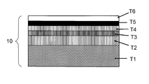
- FIG. 1 is a schematic cross-sectional view showing the configuration of a metal laminated substrate 5A for an oxide superconducting wire obtained by the production method of the present invention.
- a metal laminated substrate 5A for an oxide superconducting wire includes a nonmagnetic metal plate T1 serving as a metal substrate, a copper foil T2 (copper layer) laminated on the nonmagnetic metal plate T1, and a copper foil T2.
- the nonmagnetic metal plate T1 is used for the role of a copper foil reinforcing plate, and has a higher strength than a nonmagnetic (antiferromagnetic or paramagnetic) copper foil under 77K where an oxide superconducting wire is used. Can be mentioned. Further, the nonmagnetic metal plate T1 is preferably a softened state, that is, a so-called annealed material (O material). The reason for this is to use a copper foil that has been cold-rolled and hardened at a high pressure reduction rate to secure the contact area of the above-mentioned bonding interface under a low pressure as much as possible, and to reduce warping after rolling. It is.
- the nonmagnetic metal plate T1 include, for example, an annealed material of a stainless steel plate such as SUS316L.
- the thickness is preferably 0.05 mm or more and 0.2 mm or less. The reason why the thickness is 0.05 mm or more is to ensure the strength of the nonmagnetic metal plate T1, and the reason why the thickness is 0.2 mm or less is to ensure workability when processing the superconductor.
- the copper foil T2 it is preferable to use a so-called full-hard material made of copper or a copper alloy that is cold-rolled at a reduction rate of 90% or more (in the present specification, both may be referred to as a copper foil).
- the reason why the rolling reduction is 90% or more is that Cu may not be oriented in a heat treatment performed later in a copper foil having a rolling reduction of less than 90%.
- the thickness of the copper foil T2 is preferably 7 ⁇ m or more and 50 ⁇ m or less from the viewpoint of strength and workability.
- the composition of copper foil adds 100 ppm or more and 1% or less in total of additive elements, such as Ag, Sn, Zn, Zr, O, and N, in Cu base.
- additive elements such as Ag, Sn, Zn, Zr, O, and N
- the total amount of these additive elements exceeds 1%, oxides and the like are formed in the Cu matrix, which adversely affects the surface cleanliness.
- the crystal orientation may be deteriorated.
- the effect of Ag addition is particularly effective for improving crystal orientation, and the amount of Ag added is preferably 200 ppm to 300 ppm.
- the metal laminated substrate manufactured by the manufacturing method of this embodiment is for oxide superconducting wires, and an oxide intermediate layer such as CeO 2 or YSZ is formed in a high-temperature oxidizing atmosphere at 600 ° C. or higher in a later step. Is done. Therefore, coating the oxide intermediate layer directly on the copper surface may make it difficult to ensure uniform adhesion due to the surface oxidation of the copper. After the heat treatment, Ni on the copper foil surface may be difficult. It is preferred to coat the layer.
- the Ni layer coating method may be any epitaxial growth method so as to inherit the high biaxial crystal orientation of the copper foil.
- the electrolytic Ni plating method is preferable. Any electrolytic Ni plating bath may be used as long as it is matte plating or semi-gloss plating such as a normal watt bath, chloride bath or sulfamic acid bath.
- the thickness of the Ni plating layer should be as thin as possible.
- the thickness should be set to 1 ⁇ m to 3 ⁇ m. preferable.
- the Ni film includes a Ni alloy film.
- the metal laminated substrate for oxide superconducting wire 5A shown in FIG. 1 is laminated by bonding the nonmagnetic metal plate T1 and the copper foil T2 with a rolling roll after washing.
- the cleaning method may be any of dry, wet, wet / dry combined use.
- a process such as sputtering with an inert gas (Ar, Ne, etc.) or etching with an ion beam in a vacuum.
- a wet type after dipping into a general sulfuric acid pickling or alkaline cleaning solution, it is washed with water and dried after a degreasing treatment by electrolysis.
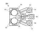
- the vacuum clad continuous device D1 as shown in FIG. 5 continuously performs dry etching before the rolling by the rolling roll, A method of removing the oxide film layer is preferably employed.
- a nonmagnetic metal plate L1 and a copper foil L2 are prepared as long coils having a width of 150 mm to 600 mm, and are installed in the recoiler parts S1 and S2 of the surface activated bonding apparatus D1.
- the non-magnetic metal plate L1 and the copper foil L2 conveyed from the recoiler parts S1 and S2 are continuously conveyed to the surface activation treatment step, and after the two surfaces to be joined are activated in advance, cold welding is performed. To do.
- the nonmagnetic metal plate L1 and the copper foil L2 having the joint surface are each grounded and grounded as one electrode A (S3), and the other electrode B (S4) that is insulated and supported.
- Glow discharge is generated by applying an alternating current of 1 to 50 MHz, and the area of the electrode exposed in the plasma generated by the glow discharge is sputter-etched so that it is 1/3 or less of the area of the electrode B.
- the inert gas argon, neon, xenon, krypton, or a mixed gas containing at least one of these can be used.
- the surface to be joined is sputtered with an inert gas to remove the surface adsorption layer and the surface oxide film, and the surface to be joined is activated by sputtering the nonmagnetic metal plate L1 and the copper foil L2.
- the electrode A (S3) takes the form of a cooling roll to prevent the temperature of each conveying material from rising.
- the adsorbate on the bonding surface is completely removed, but the surface oxide layer does not have to be completely removed. Even if an oxide layer remains on the entire surface, it is possible to ensure the bondability between the metal plate and the copper foil by increasing the rolling reduction in the bonding process and exposing the substrate by friction at the bonding surface. is there.
- the recrystallization start temperature of the copper foil is around 150 ° C.
- the copper foil temperature rises to 150 ° C. or higher during the sputter etching process the copper foil recrystallizes and the copper foil is crystallized before bonding. It will be.
- strain introduced into the copper foil and the biaxial crystal orientation of the copper foil is deteriorated.
- the strain introduced by rolling is slight, even if the subsequent heat treatment is performed, the crystal orientation cannot be highly achieved. For this reason, it is necessary to keep the temperature of the copper foil below 150 ° C. in the sputter etching process.
- the metal plate is processed at a high plasma output or the temperature of the metal plate is increased to 150 ° C. or more over time, the metal plate is heated depending on the vacuum conditions, The copper foil temperature increases due to contact with the copper foil, and recrystallization of the copper foil occurs simultaneously with rolling, which may deteriorate the biaxial crystal orientation. For this reason, it is desirable to keep the temperature of the metal plate below 150 ° C. even in the sputter etching process of the nonmagnetic metal plate. Preferably, it is kept at room temperature to 100 ° C.
- the degree of vacuum at this time is preferably higher in order to prevent re-adsorbed substances on the surface, but it may be 10 ⁇ 5 Pa or more and 10 ⁇ 2 Pa or less.
- pressure bonding is performed in a non-oxidizing atmosphere, for example, an inert gas atmosphere such as Ar. Is also preferable.
- the pressing by the rolling roll is preferably performed in order to secure a close contact area at the bonding interface, and to peel off a part of the surface oxide film layer by friction occurring at the bonding interface during the reduction to expose the substrate, and to apply 300 MPa or more.
- the metal plate is a strength reinforcing material
- the copper foil to be bonded is also full hard, and both materials are hard. Therefore, pressurization at 600 MPa to 1.5 GPa is preferable.
- the pressurization may be applied more than this, and it has been confirmed that the crystal orientation does not deteriorate after the subsequent heat treatment up to a reduction rate of 30%. However, if further processing is applied, cracks are generated on the surface of the copper foil, and the crystal orientation of the copper foil after rolling and heat treatment becomes poor.
- the laminated body After joining the copper foil and the nonmagnetic metal plate by the rolling roll, the laminated body is heat-treated in order to crystallize the copper foil, and after the copper foil T2 is biaxially crystallized, the copper foil T2 side surface is protected. Layer T3 is formed.
- the heat treatment temperature may be 150 ° C. or more as long as the copper foil and the nonmagnetic metal plate are sufficiently adhered.
- an annealed material of a stainless steel plate is used as the nonmagnetic metal plate, the strength hardly changes by heat treatment. Even when a rolled material that is not annealed is used, even if the heat treatment time is about 1 to 10 minutes even at a high temperature of 600 ° C. or higher, there is no significant decrease in strength, and the role as a strength reinforcing material is sufficiently fulfilled.
- Table 1 shows the results when the high pressure lower copper foil added with 200 ppm of Ag having a width of 200 mm and a thickness of 18 ⁇ m and SUS316L (annealed material) having a thickness of 100 ⁇ m were passed through using a surface activated bonding apparatus as shown in FIG.
- the relationship between Ar sputter etching time and the pressurization with the rolling roll in the subsequent joining process and the adhesion strength (180 degree peel strength) of the joined material is shown.
- the plasma output was 200 W under 0.1 Pa
- the plate passing speed was changed
- the sputter irradiation time to the bonding surface was changed.
- the joining was performed by changing the pressure on the rolling roll from 100 MPa to 1500 MPa.
- the sample after bonding had a (200) plane C-axis crystal orientation measured by ⁇ / 2 ⁇ measurement by X-ray diffraction. It was measured.
- the (200) plane crystal orientation ratio up to 30% was regarded as no occurrence of crystal orientation (recrystallization).
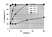
- FIG. 6 shows the relationship between the crystal orientation rate and the heat treatment holding time of the rolled copper foil (200) surface with 200 ppm Ag added. After the heat treatment, the crystal orientation ratio was measured by ⁇ / 2 ⁇ using an X-ray diffractometer, and the C-axis orientation of the (200) plane was measured.
- the C-axis orientation is the X-ray diffraction intensity (200) plane of the total (represented as ⁇ I (hkl)) of the (111) plane, (200) plane, (220) plane, and (311) plane (represented as ⁇ I (hkl)).
- (200) plane crystal orientation ratio I (200) / ⁇ I ⁇ 100 (%).
- the (200) plane is about 20% to 30% in the rolled state without heat treatment. From FIG. 6, it can be seen that there is no change in the crystal orientation when the heat treatment is lower than 150 ° C. for about 1 minute. However, when the temperature is maintained further, particularly at a temperature of 150 ° C. or higher, the recrystallization of copper proceeds rapidly and the (200) plane increases rapidly.
- the sputter etching time is increased to 60 seconds and 300 seconds, and when the adsorbate and the surface oxide layer are removed, the adhesion strength increases, but during sputter etching. Then, copper recrystallizes and crystal orientation occurs.
- the thicknesses of the oxide films of the copper foil and the stainless steel plate used in this experiment were 5 nm and 10 nm, respectively, as measured by an Auger electron microscope before bonding.
- the Ar sputtering rate at an RF output of 200 W was obtained by measuring the sputtering rate of copper and stainless steel based on the sputtering rate by standard measurement of sputtering of Si. For example, in order to completely remove the oxide film on the stainless steel surface, it took 5 minutes at an RF output of 200 W in the sputtering apparatus in the present bonding apparatus.
- the surface state described in the remarks column in Table 1 is assumed to be the surface state after sputter etching.
- Table 2 shows the degree of (200) plane crystal orientation on the copper foil side after the Cu / SUS316L laminated substrate shown in Example 1 is held at 150 ° C. to 950 ° C. for 5 minutes to 4 hours in a non-oxidizing atmosphere, and heat treatment Later, the (200) plane crystal orientation degree and the C-axis crystal orientation ratio of the protective layer (Ni layer) when 1 ⁇ m thick Ni plating is applied to the copper foil surface side are shown together with comparative experimental examples.
- the Ni plating was performed using a general Watt bath at a current density of 4 A / dm 2 , a bath temperature of 60 ° C., and a pH of 3.
- ⁇ of copper when heat-treating the metal laminated substrate of Comparative Experimental Example 1-5 (sputtering time 120 seconds, pressure 300 MPa) shown in Example 1 is also shown.
- This sample has crystallized once before bonding, and after that, since 300 MPa is applied in the bonding process, strain is introduced. Therefore, the biaxial crystal orientation is deteriorated even after the heat treatment, and ⁇ shows a value of 6 ° or more. Further, when this sample is heat-treated at a relatively high temperature of 850 ° C., secondary recrystallization occurs due to the introduction of strain, and the crystal orientation is greatly lost.
- FIG. 2 is a schematic cross-sectional view showing a configuration of an oxide superconducting wire 10A in which an intermediate layer T4, an oxide superconductor layer T5, and a protective film T6 are sequentially laminated on the metal laminated substrate 5A for oxide superconducting wire shown in FIG. It is.
- the oxide superconducting wire 10A is formed by epitaxially depositing an intermediate layer such as CeO 2 , YSZ, SrTiO 3 , or MgO on the protective layer T3 using a sputtering method or the like, and forming a superconductor layer such as a Y123-based thin film using a laser ablation method or the like. It is manufactured by forming a film and laminating Ag, Cu or the like as a protective film on the superconductor layer.
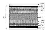
- FIG. 3 shows a metal laminate for an oxide superconducting wire.
- a copper foil T2 is applied to both surfaces of a nonmagnetic metal plate T1 by surface activation bonding, and after heat treatment, a Ni layer protective layer T3 is applied to both surfaces.
- FIG. 4 is a schematic cross-sectional view showing a configuration of an oxide superconducting wire 10B using the metal laminated plate for oxide superconducting wire shown in FIG.
- the heat treatment is performed to crystallize the copper, so that copper is highly oriented compared to the prior art and prevents the formation of scratches and grooves on the surface. It is possible to stack copper on the substrate with less change in copper reduction than in the prior art by sputter etching copper while maintaining the temperature below the crystal start temperature of copper, and then heating Compared with the prior art, copper can be highly oriented when orienting copper that has been reduced by processing. Furthermore, since copper is sputter-etched at a temperature lower than the crystal start temperature of copper, there is a high possibility that an oxide layer will remain on the copper surface. With conventional technology, the adhesion between copper and the substrate tends to decrease. In the invention, by controlling the pressing conditions, the adhesion required for the substrate can be realized simultaneously with the high orientation of copper, and the industrial applicability is extremely high.
Abstract
Description
これらの酸化物膜の成膜方法には、従来、イオン・アシスト・ビーム成膜法(IBAD法)や、予め結晶配向させた金属基板上に酸化物を成膜していくRABITS法が知られている。 In order to obtain an excellent high-temperature oxide superconducting wire, an intermediate layer (CeO 2 or zirconia-added yttrium oxide (YSZ)) and a superconducting film (RE123 film: RE: Y, Gd, Ho on a metal substrate are provided. Etc.) need to be formed.
Conventionally known oxide film deposition methods include ion-assisted beam deposition (IBAD) and RABITS, in which an oxide is deposited on a previously crystallized metal substrate. ing.
また、特許文献2に開示の製造方法は、銅を結晶配向させてから冷間圧延によりステンレス基板に積層する手段を採用しており、結晶配向した銅を圧延することになるので、この圧延により銅の配向の低下や銅の表面に傷や溝ができる場合が有る。このため、その上に積層するニッケル層、超伝導層等の配向が低下してしまい、超伝導体の特性が低下するおそれがあるという問題がある。 However, the manufacturing method disclosed in
Moreover, since the manufacturing method disclosed in
また、本発明の他の目的は、銅の圧下状態の変化を少なくして銅を基板に積層でき、その後の加熱処理により圧下された銅を配向させるときに銅を高度に配向させることができる、酸化物超電導線材用金属積層基板及びその製造方法を提供することである。
さらに、本発明の他の目的は、加圧条件を制御することで基板に求められる密着力を銅の高配向と同時に実現できる、酸化物超電導線材用金属積層基板及びその製造方法を提供することである。 The present invention provides a metal laminated substrate for an oxide superconducting wire and a method for producing the same, which can solve such problems and highly orient copper and prevent the formation of scratches and grooves on the surface. For the purpose.
In addition, another object of the present invention is to allow copper to be laminated on a substrate with less change in the reduction state of copper, and to highly orient copper when orienting copper that has been reduced by subsequent heat treatment. It is to provide a metal laminated substrate for an oxide superconducting wire and a method for producing the same.
Furthermore, another object of the present invention is to provide a metal laminated substrate for oxide superconducting wire and a method for producing the same, which can realize the adhesion required for the substrate simultaneously with the high orientation of copper by controlling the pressing conditions. It is.
圧下率90%以上で圧延加工された銅箔を結晶配向温度未満に保った状態で銅箔の表面をスパッタエッチングして表面の吸着物を除去する工程と、
非磁性の金属板の表面をスパッタエッチングして表面の吸着物を除去する工程と、
前記銅箔と前記金属板とを圧延ロールにより300MPa~1500MPaの加圧で接合する工程と、
前記接合した積層体を銅の結晶配向温度以上の温度に加熱して前記銅を結晶配向させる工程と、
前記積層体の銅側表面上に保護層をコーティングする工程と、を有することを特徴とする。
(2)本発明の酸化物超電導線材用金属積層基板の製造方法は、前記(1)において、前記銅箔のスパッタエッチングは、150℃未満の温度で実施することを特徴とする。
(3)本発明の酸化物超電導線材用金属積層基板の製造方法は、前記(1)又は(2)において、前記非磁性の金属板のスパッタエッチングする工程は、銅箔の結晶配向温度未満に保った状態で基板の表面をスパッタエッチングして表面の吸着物を除去することを特徴とする。
(4)本発明の酸化物超電導線材用金属積層基板は、
非磁性の金属板と、
前記金属板上に銅層を有し、
さらに前記銅層の上層に保護層を有する酸化物超電導線材用金属積層基板であって、
前記保護層のC軸結晶配向率が99%以上であり、
かつ、前記銅層と前記金属板の密着強度が180°ピール強度で0.1N/cm以上であることを特徴とする。 (1) The manufacturing method of the metal laminated substrate for oxide superconducting wire of the present invention includes:
A step of removing the adsorbate on the surface by sputter etching the surface of the copper foil in a state in which the copper foil rolled at a rolling reduction of 90% or more is kept below the crystal orientation temperature;
A step of sputter etching the surface of the non-magnetic metal plate to remove the adsorbate on the surface;
Bonding the copper foil and the metal plate with a pressure of 300 MPa to 1500 MPa by a rolling roll;
Heating the bonded laminate to a temperature equal to or higher than the crystal orientation temperature of copper to crystallize the copper;
And a step of coating a protective layer on the copper side surface of the laminate.
(2) The method for producing a metal laminated substrate for an oxide superconducting wire according to the present invention is characterized in that, in the above (1), the sputter etching of the copper foil is performed at a temperature of less than 150 ° C.
(3) In the method for producing a metal laminated substrate for an oxide superconducting wire according to the present invention, in the above (1) or (2), the step of sputter-etching the nonmagnetic metal plate is less than the crystal orientation temperature of the copper foil. In this state, the surface of the substrate is sputter-etched to remove the adsorbate on the surface.
(4) The metal laminated substrate for oxide superconducting wire of the present invention is
A non-magnetic metal plate,
Having a copper layer on the metal plate;
Further, a metal laminated substrate for oxide superconducting wire having a protective layer on the copper layer,
The C-axis crystal orientation of the protective layer is 99% or more,
And the adhesive strength of the said copper layer and the said metal plate is 0.1 N / cm or more by 180 degree peel strength, It is characterized by the above-mentioned.
さらに、銅の結晶配向温度未満で銅箔及び非磁性金属板の表面をスパッタエッチングすることにより、銅箔を再結晶させることなくエッチング前の銅箔と同程度の結晶状態を保ったまま吸着物を除去することができ、且つ圧下条件を制御することにより銅箔の結晶状態をエッチング前の銅箔と同程度に保持したまま十分な密着力を確保することが可能となる。このように接合条件を制御することにより、積層後もエッチング前の銅箔と同程度の結晶状態を保持することができるため、その後の加熱処理により銅を高度に結晶配向させることができる。 According to the present invention, after copper is laminated on the substrate, the heat treatment is performed to crystallize the copper, so that copper is highly oriented compared to the prior art and prevents the formation of scratches and grooves on the surface. It becomes possible to do.
Furthermore, by adhering the surface of the copper foil and non-magnetic metal plate below the crystal orientation temperature of copper, the adsorbate remains in the same crystal state as the copper foil before etching without recrystallizing the copper foil. By controlling the reduction conditions, it is possible to ensure a sufficient adhesion while maintaining the crystal state of the copper foil at the same level as that of the copper foil before etching. By controlling the bonding conditions in this manner, the crystal state can be maintained at the same level as that of the copper foil before etching even after lamination, so that the copper can be highly crystallized by subsequent heat treatment.
非磁性の金属板の表面をスパッタエッチングして表面の吸着物を除去し、
銅箔と金属板とを圧延ロールにより300MPa~1500MPaの加圧で接合し、接合した積層体を銅の結晶配向温度以上の温度に加熱して銅を結晶配向させ、積層体の銅側表面上に保護層をコーティングする。 In the method for manufacturing a metal laminated substrate for an oxide superconducting wire according to an embodiment of the present invention, the surface of the copper foil is sputter-etched with the copper foil rolled at a rolling reduction of 90% or less kept below the crystal orientation temperature. Remove the adsorbed material on the surface,
Sputter etching the surface of the non-magnetic metal plate to remove the adsorbed material on the surface,
A copper foil and a metal plate are joined with a rolling roll at a pressure of 300 MPa to 1500 MPa, and the joined laminate is heated to a temperature equal to or higher than the crystal orientation temperature of copper to crystallize copper, and on the copper side surface of the laminate The protective layer is coated on.
図1に示すように、酸化物超電導線材用金属積層基板5Aは、金属基板となる非磁性金属板T1、非磁性金属板T1の上に積層された銅箔T2(銅層)、銅箔T2の上にコーティングしたNi層(保護層)T3からなる。 FIG. 1 is a schematic cross-sectional view showing the configuration of a metal laminated substrate 5A for an oxide superconducting wire obtained by the production method of the present invention.
As shown in FIG. 1, a metal laminated substrate 5A for an oxide superconducting wire includes a nonmagnetic metal plate T1 serving as a metal substrate, a copper foil T2 (copper layer) laminated on the nonmagnetic metal plate T1, and a copper foil T2. An Ni layer (protective layer) T3 coated thereon.
非磁性金属板T1としては、銅箔の補強板の役割のために用いられ、酸化物超電導線材が使用される77K下で非磁性(反強磁性体または常磁性体)の銅箔より高強度のものが挙げられる。
また、非磁性金属板T1は、極力軟化した状態、いわゆる焼鈍材(O材)が好ましい。
この理由は、接合相手である銅箔が高圧下率で冷間圧延され硬化したものを使用するため、上述した接合界面の接触面積を極力低圧下で確保させ、圧延後の反りを低減させるためである。
非磁性金属板T1の具体例として、例えばSUS316Lなどのステンレス鋼板の焼鈍材などが挙げられ、例えば、その厚みを0.05mm以上0.2mm以下のものとすることが好ましい。
0.05mm以上とする理由は非磁性金属板T1の強度の確保であり、0.2mm以下とする理由は超伝導材を加工するときの加工性確保のためである。 <Non-magnetic metal plate>
The nonmagnetic metal plate T1 is used for the role of a copper foil reinforcing plate, and has a higher strength than a nonmagnetic (antiferromagnetic or paramagnetic) copper foil under 77K where an oxide superconducting wire is used. Can be mentioned.
Further, the nonmagnetic metal plate T1 is preferably a softened state, that is, a so-called annealed material (O material).
The reason for this is to use a copper foil that has been cold-rolled and hardened at a high pressure reduction rate to secure the contact area of the above-mentioned bonding interface under a low pressure as much as possible, and to reduce warping after rolling. It is.
Specific examples of the nonmagnetic metal plate T1 include, for example, an annealed material of a stainless steel plate such as SUS316L. For example, the thickness is preferably 0.05 mm or more and 0.2 mm or less.
The reason why the thickness is 0.05 mm or more is to ensure the strength of the nonmagnetic metal plate T1, and the reason why the thickness is 0.2 mm or less is to ensure workability when processing the superconductor.
銅箔T2は、圧下率90%以上で冷間圧延された銅若しくは銅合金(本明細書においては両者を併せて銅箔という場合がある)からなる、いわゆるフルハード材を用いることが好ましい。
圧下率90%以上とする理由は、圧下率90%未満の銅箔は、後に行う熱処理においてCuが配向しないおそれがあるからである。
また、銅箔T2の厚みは、強度面や加工性の点から、厚み7μm以上50μm以下のものが好ましい。 <Copper foil>
As the copper foil T2, it is preferable to use a so-called full-hard material made of copper or a copper alloy that is cold-rolled at a reduction rate of 90% or more (in the present specification, both may be referred to as a copper foil).
The reason why the rolling reduction is 90% or more is that Cu may not be oriented in a heat treatment performed later in a copper foil having a rolling reduction of less than 90%.
The thickness of the copper foil T2 is preferably 7 μm or more and 50 μm or less from the viewpoint of strength and workability.
これらの元素を100ppm以上添加することで、Cuを固溶強化するとともに、結晶配向性が純銅に比べ向上し、同じ圧下率で、より高い2軸配向性を得ることができる。しかしながら、これらの添加元素のトータル添加量が1%を超えると、Cu基地中に酸化物などが形成され、表面清浄性に悪影響を及ぼす。また、結晶配向性が悪くなる場合もある。
さらに、上記添加元素の中でも、Ag添加の効果は結晶配向性の向上に特に効果があり、Ag添加量を200ppm~300ppmとすることが好ましい。 In addition, it is preferable that the composition of copper foil adds 100 ppm or more and 1% or less in total of additive elements, such as Ag, Sn, Zn, Zr, O, and N, in Cu base.
By adding 100 ppm or more of these elements, while strengthening solid solution of Cu, crystal orientation is improved as compared with pure copper, and higher biaxial orientation can be obtained with the same rolling reduction. However, if the total amount of these additive elements exceeds 1%, oxides and the like are formed in the Cu matrix, which adversely affects the surface cleanliness. In addition, the crystal orientation may be deteriorated.
Further, among the above additive elements, the effect of Ag addition is particularly effective for improving crystal orientation, and the amount of Ag added is preferably 200 ppm to 300 ppm.
本実施形態の製造方法によって製造される金属積層基板は、酸化物超電導線材用であり、後の工程にてCeO2やYSZなどの酸化物中間層が600℃以上の高温酸化雰囲気中で成膜される。そのため、直接銅表面上に上記酸化物中間層をコーティングすることは、銅の表面酸化が起因で密着性を均一に確保することが困難となる場合があり、上記熱処理後に銅箔表面上にNi層をコーティングすることが好ましい。 <Protective layer>
The metal laminated substrate manufactured by the manufacturing method of this embodiment is for oxide superconducting wires, and an oxide intermediate layer such as CeO 2 or YSZ is formed in a high-temperature oxidizing atmosphere at 600 ° C. or higher in a later step. Is done. Therefore, coating the oxide intermediate layer directly on the copper surface may make it difficult to ensure uniform adhesion due to the surface oxidation of the copper. After the heat treatment, Ni on the copper foil surface may be difficult. It is preferred to coat the layer.
電解Niメッキ浴は、通常のワット浴、塩化物浴やスルファミン酸浴などの無光沢メッキおよび半光沢メッキであれば何れの浴を用いて実施してもよい。 The Ni layer coating method may be any epitaxial growth method so as to inherit the high biaxial crystal orientation of the copper foil. However, in consideration of productivity, the electrolytic Ni plating method is preferable.
Any electrolytic Ni plating bath may be used as long as it is matte plating or semi-gloss plating such as a normal watt bath, chloride bath or sulfamic acid bath.
図1に示す酸化物超電導線材用金属積層基板5Aは、非磁性金属板T1と銅箔T2とを洗浄後、圧延ロールで接合して積層する。
洗浄方法は、乾式、湿式、湿式・乾式併用、いずれの方法で行っても良い。
乾式の場合、真空中での不活性ガス(Ar、Neなど)によるスパッタ、イオンビームによるエッチングなどの処理を実行することが好ましい。
湿式の場合、一般の硫酸酸洗、アルカリ洗浄液などへのディップした後、電解による脱脂処理後、水洗、乾燥するようにする。
なお、金属板と銅箔との接合処理の生産性を考えると、図5に示すような真空クラッド連続装置D1で、圧延ロールによる圧下前に連続的に乾式エッチングを行い、表面の吸着層や酸化膜層を除去する方法が好ましく採用される。 <Manufacturing method>
The metal laminated substrate for oxide superconducting wire 5A shown in FIG. 1 is laminated by bonding the nonmagnetic metal plate T1 and the copper foil T2 with a rolling roll after washing.
The cleaning method may be any of dry, wet, wet / dry combined use.
In the case of a dry process, it is preferable to perform a process such as sputtering with an inert gas (Ar, Ne, etc.) or etching with an ion beam in a vacuum.
In the case of a wet type, after dipping into a general sulfuric acid pickling or alkaline cleaning solution, it is washed with water and dried after a degreasing treatment by electrolysis.
In consideration of the productivity of the joining treatment between the metal plate and the copper foil, the vacuum clad continuous device D1 as shown in FIG. 5 continuously performs dry etching before the rolling by the rolling roll, A method of removing the oxide film layer is preferably employed.
このような理由から、スパッタエッチング工程では、銅箔の温度を150℃未満に保持する必要がある。好ましくは、常温~100℃以下に保持する。 Further, when the oxide layer is completely removed by dry etching, high plasma output or long-time etching is required, and the material temperature rises. Since the recrystallization start temperature of the copper foil is around 150 ° C., when the copper foil temperature rises to 150 ° C. or higher during the sputter etching process, the copper foil recrystallizes and the copper foil is crystallized before bonding. It will be. When a crystal-oriented copper foil is rolled, strain is introduced into the copper foil and the biaxial crystal orientation of the copper foil is deteriorated. In this case, since the strain introduced by rolling is slight, even if the subsequent heat treatment is performed, the crystal orientation cannot be highly achieved.
For this reason, it is necessary to keep the temperature of the copper foil below 150 ° C. in the sputter etching process. Preferably, it is kept at room temperature to 100 ° C. or less.
このため、非磁性の金属板のスパッタエッチング工程においても、金属板の温度を150℃未満に保つことが望ましい。好ましくは常温~100℃に保つことがよい。 この時の真空度は、表面への再吸着物を防止するため高い方が好ましいが、10-5Pa以上10-2Pa以下であればよい。 Also, in the process of sputter etching a non-magnetic metal plate, if the metal plate is processed at a high plasma output or the temperature of the metal plate is increased to 150 ° C. or more over time, the metal plate is heated depending on the vacuum conditions, The copper foil temperature increases due to contact with the copper foil, and recrystallization of the copper foil occurs simultaneously with rolling, which may deteriorate the biaxial crystal orientation.
For this reason, it is desirable to keep the temperature of the metal plate below 150 ° C. even in the sputter etching process of the nonmagnetic metal plate. Preferably, it is kept at room temperature to 100 ° C. The degree of vacuum at this time is preferably higher in order to prevent re-adsorbed substances on the surface, but it may be 10 −5 Pa or more and 10 −2 Pa or less.
スパッタエッチングにより吸着物層を除去し、300MPa以上の加圧により、接合の密着強度は180°ピール強度で0.1N/cm以上を得ることができる。
特に、金属板は強度補強材であり、貼り合わせる銅箔もフルハードとなっており、両材料とも硬い。そのため600MPa以上1.5GPa以下での加圧が好ましい。
加圧はこれ以上かけてもよく、圧下率で30%までは後の熱処理後に結晶配向性が劣化しないことは確認している。
しかしながら、これ以上の加工を加えると、銅箔表面にクラックが発生するとともに圧延、熱処理後の銅箔の結晶配向性が悪くなる。 The pressing by the rolling roll is preferably performed in order to secure a close contact area at the bonding interface, and to peel off a part of the surface oxide film layer by friction occurring at the bonding interface during the reduction to expose the substrate, and to apply 300 MPa or more.
By removing the adsorbed material layer by sputter etching and applying a pressure of 300 MPa or more, it is possible to obtain a bonding strength of 0.1 N / cm or more at a 180 ° peel strength.
In particular, the metal plate is a strength reinforcing material, the copper foil to be bonded is also full hard, and both materials are hard. Therefore, pressurization at 600 MPa to 1.5 GPa is preferable.
The pressurization may be applied more than this, and it has been confirmed that the crystal orientation does not deteriorate after the subsequent heat treatment up to a reduction rate of 30%.
However, if further processing is applied, cracks are generated on the surface of the copper foil, and the crystal orientation of the copper foil after rolling and heat treatment becomes poor.
本実施形態では、非磁性の金属板としてステンレス鋼板の焼鈍材を用いた場合、熱処理で強度はほとんど変化しない。
また、焼鈍を行わない圧延材を用いた場合でも、600℃以上の高温においても熱処理時間が1分~10分程度では大きな強度低下はなく、強度補強材としての役割を十分果たす。 After joining the copper foil and the nonmagnetic metal plate by the rolling roll, the laminated body is heat-treated in order to crystallize the copper foil, and after the copper foil T2 is biaxially crystallized, the copper foil T2 side surface is protected. Layer T3 is formed. The heat treatment temperature may be 150 ° C. or more as long as the copper foil and the nonmagnetic metal plate are sufficiently adhered.
In this embodiment, when an annealed material of a stainless steel plate is used as the nonmagnetic metal plate, the strength hardly changes by heat treatment.
Even when a rolled material that is not annealed is used, even if the heat treatment time is about 1 to 10 minutes even at a high temperature of 600 ° C. or higher, there is no significant decrease in strength, and the role as a strength reinforcing material is sufficiently fulfilled.
表1は、幅200mmで厚み18μmのAgが200ppm添加された高圧下銅箔および100μm厚のSUS316L(焼鈍材)を、図5のような表面活性化接合装置を用い、通板させたときのArスパッタエッチング時間とその後の接合工程での圧延ロールでの加圧と接合した材料の密着強度(180°ピール強度)との関係を示している。
スパッタエッチングは、0.1Pa下で、プラズマ出力を200Wとし、通板速度を変化させ接合面へのスパッタ照射時間を変化させた。
また圧延ロールでの加圧を100MPa~1500MPaと変化させて接合を行った。また、銅がスパッタエッチング中、温度上昇し、結晶構造が変化しなかったかを確認するため、接合後のサンプルは、X線回折によるθ/2θ測定により、(200)面のC軸結晶配向を測定した。
ここでは接合後、(200)面結晶配向率30%までを結晶配向(再結晶)発生なしとし、それ以上の場合を(200)面結晶配向が発生したと判断した。
Hereinafter, the manufacturing method of the metal laminated substrate for oxide superconducting wire of the present invention will be described in more detail by way of examples.
Table 1 shows the results when the high pressure lower copper foil added with 200 ppm of Ag having a width of 200 mm and a thickness of 18 μm and SUS316L (annealed material) having a thickness of 100 μm were passed through using a surface activated bonding apparatus as shown in FIG. The relationship between Ar sputter etching time and the pressurization with the rolling roll in the subsequent joining process and the adhesion strength (180 degree peel strength) of the joined material is shown.
In the sputter etching, the plasma output was 200 W under 0.1 Pa, the plate passing speed was changed, and the sputter irradiation time to the bonding surface was changed.
Further, the joining was performed by changing the pressure on the rolling roll from 100 MPa to 1500 MPa. In addition, in order to confirm whether the temperature of the copper rose during sputter etching and the crystal structure did not change, the sample after bonding had a (200) plane C-axis crystal orientation measured by θ / 2θ measurement by X-ray diffraction. It was measured.
Here, after bonding, the (200) plane crystal orientation ratio up to 30% was regarded as no occurrence of crystal orientation (recrystallization).

図6は、200ppmAg添加の圧延銅箔(200)面の、結晶配向率と熱処理保持時間との関係を示している。
熱処理後、結晶配向率は、X線回折装置にてθ/2θ測定を行い、(200)面のC軸配向について測定を行った。
C軸配向は、(111)面、(200)面、(220)面および(311)面のX線回折強度のトータル(ΣI(hkl)と表す)の(200)面のX線回折強度(I(200)と表す)の割合を示し、(200)面結晶配向率=I(200)/ΣI×100(%)で表される。
本実施例で用いる銅箔では、熱処理なしの圧延加工状態では、(200)面は20%~30%程度である。
図6より、150℃より低い熱処理において、1分程度保持では結晶配向に変化はないことが分かる。
しかしながら、それ以上保持した場合、特に150℃以上の温度では、銅の再結晶は急速に進行し、(200)面が急激に増加していく。 Here, the reason for measuring the (200) plane C-axis crystal orientation of the sample after bonding by θ / 2θ measurement by X-ray diffraction will be described with reference to FIG.
FIG. 6 shows the relationship between the crystal orientation rate and the heat treatment holding time of the rolled copper foil (200) surface with 200 ppm Ag added.
After the heat treatment, the crystal orientation ratio was measured by θ / 2θ using an X-ray diffractometer, and the C-axis orientation of the (200) plane was measured.
The C-axis orientation is the X-ray diffraction intensity (200) plane of the total (represented as ΣI (hkl)) of the (111) plane, (200) plane, (220) plane, and (311) plane (represented as ΣI (hkl)). (200) plane crystal orientation ratio = I (200) / ΣI × 100 (%).
In the copper foil used in this example, the (200) plane is about 20% to 30% in the rolled state without heat treatment.
From FIG. 6, it can be seen that there is no change in the crystal orientation when the heat treatment is lower than 150 ° C. for about 1 minute.
However, when the temperature is maintained further, particularly at a temperature of 150 ° C. or higher, the recrystallization of copper proceeds rapidly and the (200) plane increases rapidly.
すなわち、本発明における製造方法において、銅箔と金属基板の接合を、接合前、スパッタエッチングを行う場合、高出力で処理時間が長くなると、プラズマで銅箔温度が上昇し、銅箔が再結晶を起こし、接合前に結晶配向してしまうおそれがある。
その場合、圧接工程のロール圧延で銅箔に歪みが導入され結晶配向が劣化してしまう。一旦高圧下で加工した銅箔が再結晶によって高結晶配向状態が得られても、その後に歪が導入され、配向が劣化すると、熱処理などにより結晶配向を回復させようとしても難しい。
よって、スパッタエッチングにおいては、少なくとも150℃未満に保持され、極力短時間で処理することが必要となる。 From this, the following can be said.
That is, in the manufacturing method of the present invention, when sputter etching is performed before bonding the copper foil and the metal substrate, when the processing time is increased at a high output, the copper foil temperature is increased by plasma, and the copper foil is recrystallized. And crystal orientation may occur before bonding.
In such a case, strain is introduced into the copper foil by roll rolling in the pressure welding process, and the crystal orientation deteriorates. Even if a copper foil once processed under high pressure has a high crystal orientation state by recrystallization, if strain is introduced and the orientation deteriorates, it is difficult to recover the crystal orientation by heat treatment or the like.
Therefore, in sputter etching, it is necessary to keep the temperature at least below 150 ° C. and to process in as short a time as possible.
表1から次のようなことがわかる。すなわち、スパッタエッチングをかけない場合(0秒)や、また2秒と短時間で吸着物が完全に除去できていない場合は、加圧を1500MPaまで上げても密着しない(密着強度=0)。この結果を、比較実験例1~4に示す。 Next, the characteristic result of the Cu / SUS316L laminated metal substrate before Ni layer coating is shown with a comparative example.
Table 1 shows the following. That is, when sputter etching is not applied (0 seconds), or when the adsorbate has not been completely removed in a short time of 2 seconds, adhesion does not occur even when the pressure is increased to 1500 MPa (adhesion strength = 0). The results are shown in Comparative Experimental Examples 1 to 4.
この結果を、比較実験例5に示す。 In addition, when the etching time is extended (20 seconds) and the oxide film remains, but the adsorbate is completely removed, there is almost no adhesion strength even when the pressure applied by the rolling roll is as low as 100 MPa (adhesion strength). = 0).
The results are shown in Comparative Experimental Example 5.
RF出力200WでのArスパッタ速度は、Siのスパッタを標準測定し、スパッタリング率により銅及びステンレスのスパッタ速度を求めた。
例えば、ステンレス表面の酸化膜を完全に除去するには、本接合装置中のスパッタ装置ではRF出力200Wで5分であった。
表1の備考欄に記載の表面状態は、このようなことからスパッタエッチング後の表面状態が想定される。
このようなスパッタ技術について、装置の取扱い、膜の測定、評価法などについて以下の文献を参考にした。
参考文献:スパッタ法による薄膜作成技術(装置の取扱い・膜の測定・評価と各種応用の実際)P.29、
発行所:経営開発センター出版(1985年) Here, the thicknesses of the oxide films of the copper foil and the stainless steel plate used in this experiment were 5 nm and 10 nm, respectively, as measured by an Auger electron microscope before bonding.
The Ar sputtering rate at an RF output of 200 W was obtained by measuring the sputtering rate of copper and stainless steel based on the sputtering rate by standard measurement of sputtering of Si.
For example, in order to completely remove the oxide film on the stainless steel surface, it took 5 minutes at an RF output of 200 W in the sputtering apparatus in the present bonding apparatus.
The surface state described in the remarks column in Table 1 is assumed to be the surface state after sputter etching.
Regarding such sputtering technology, the following documents were referred to for handling the apparatus, measuring the film, and evaluating the method.
Reference: Thin film fabrication technology by sputtering method (handling of equipment, measurement / evaluation of film, and actual application) 29,
Publisher: Management Development Center Publishing (1985)
Niメッキは、一般のワット浴を使用し、電流密度を4A/dm2、浴温度を60℃、pH3で行った。また、結晶配向度は、X線回折装置を用い、Cu(111)およびNi(111)の極点図を測定し、α=35°に現れる4本ピークの半値幅△Φ(°)を測定した。 Table 2 shows the degree of (200) plane crystal orientation on the copper foil side after the Cu / SUS316L laminated substrate shown in Example 1 is held at 150 ° C. to 950 ° C. for 5 minutes to 4 hours in a non-oxidizing atmosphere, and heat treatment Later, the (200) plane crystal orientation degree and the C-axis crystal orientation ratio of the protective layer (Ni layer) when 1 μm thick Ni plating is applied to the copper foil surface side are shown together with comparative experimental examples.
The Ni plating was performed using a general Watt bath at a current density of 4 A / dm 2 , a bath temperature of 60 ° C., and a pH of 3. The degree of crystal orientation was determined by measuring the pole figure of Cu (111) and Ni (111) using an X-ray diffractometer and measuring the half-value width ΔΦ (°) of the four peaks appearing at α = 35 °. .

すなわち、実施例1で示した良好な条件(スパッタ時間20秒、加圧600MPa)で作製したCu/SUS316L積層金属板を100℃で1分間熱処理しても銅は再結晶しないため、2軸結晶配向は起こらないが、150℃では30分以上、それ以上の温度ではさらに短時間の保持でΔΦは6°以下となる。
特に、150℃と低温で熱処理する場合は、保持時間を長時間するとΔΦは低下、つまり2軸結晶配向性は向上する。
また、高温短時間で熱処理する場合では、温度の上昇とともにΔΦは低下し、2軸結晶配向性が向上していく。 The following can be seen from the results in Table 2.
That is, since Cu does not recrystallize even if it heat-processes the Cu / SUS316L laminated metal plate produced on the favorable conditions (sputtering
In particular, when heat treatment is performed at a low temperature of 150 ° C., ΔΦ decreases, that is, the biaxial crystal orientation improves when the holding time is extended.
Further, when heat treatment is performed at a high temperature for a short time, ΔΦ decreases as the temperature increases, and the biaxial crystal orientation improves.
このサンプルは、接合前に一度結晶配向を起こし、その後接合工程で300MPaの加圧がなされているため、歪が導入されている。
そのため、熱処理後においても2軸結晶配向性は劣化しており、ΔΦは6°以上の値を示している。
また、このサンプルを850℃と比較的高温で熱処理すると、歪導入が原因で2次再結晶が発生し、結晶配向性が大きく崩れてしまう。
<本発明の参考形態> As a comparative example, ΔΦ of copper when heat-treating the metal laminated substrate of Comparative Experimental Example 1-5 (sputtering time 120 seconds, pressure 300 MPa) shown in Example 1 is also shown.
This sample has crystallized once before bonding, and after that, since 300 MPa is applied in the bonding process, strain is introduced.
Therefore, the biaxial crystal orientation is deteriorated even after the heat treatment, and ΔΦ shows a value of 6 ° or more.
Further, when this sample is heat-treated at a relatively high temperature of 850 ° C., secondary recrystallization occurs due to the introduction of strain, and the crystal orientation is greatly lost.
<Reference form of the present invention>
図2は、図1の酸化物超電導線材用金属積層基板5A上に、中間層T4、酸化物超電導体層T5、保護膜T6を、順次積層した酸化物超電導線材10Aの構成を示す概略断面図である。
酸化物超電導線材10Aは、保護層T3上に、CeO2、YSZ、SrTiO3、MgOなどの中間層をスパッタ法など用いてエピタキシャル成膜し、Y123系薄膜などの超電導体層をレーザーアブレージョン法などにより成膜し、この超電導体層の上にさらに保護膜としてAg、Cuなどを積層することにより製造される。 Below, the reference form manufactured using the manufacturing method of this invention is shown.
FIG. 2 is a schematic cross-sectional view showing a configuration of an oxide superconducting wire 10A in which an intermediate layer T4, an oxide superconductor layer T5, and a protective film T6 are sequentially laminated on the metal laminated substrate 5A for oxide superconducting wire shown in FIG. It is.
The oxide superconducting wire 10A is formed by epitaxially depositing an intermediate layer such as CeO 2 , YSZ, SrTiO 3 , or MgO on the protective layer T3 using a sputtering method or the like, and forming a superconductor layer such as a Y123-based thin film using a laser ablation method or the like. It is manufactured by forming a film and laminating Ag, Cu or the like as a protective film on the superconductor layer.
T2、L2 銅箔、
T3 保護層(Ni層)、
T4 中間層、
T5 酸化物超電導体層、
T6 保護膜、
D1 表面活性化接合装置、
S1,S2 リコイラー部、
S3 電極A、
S4 電極B、
S5 圧接ロール工程、
S6 巻き取り工程、
5A 金属積層基板、
5B 金属積層板、
10A、10B 酸化物超電導線材 T1, L1 non-magnetic metal plate,
T2, L2 copper foil,
T3 protective layer (Ni layer),
T4 middle layer,
T5 oxide superconductor layer,
T6 protective film,
D1 surface activated bonding device,
S1, S2 Recoiler part,
S3 electrode A,
S4 electrode B,
S5 pressure roll process,
S6 winding process,
5A metal laminated substrate,
5B metal laminate,
10A, 10B oxide superconducting wire
Claims (4)
- 圧下率90%以上で圧延加工された銅箔を結晶配向温度未満に保った状態で銅箔の表面をスパッタエッチングして表面の吸着物を除去する工程と、
非磁性の金属板の表面をスパッタエッチングして表面の吸着物を除去する工程と、
前記銅箔と前記金属板とを圧延ロールにより300MPa~1500MPaの加圧で接合する工程と、
前記接合した積層体を銅の結晶配向温度以上の温度に加熱して前記銅を結晶配向させる工程と、
前記積層体の銅側表面上に保護層をコーティングする工程と、を有することを特徴とする酸化物超電導線材用金属積層基板の製造方法。 A step of removing the adsorbate on the surface by sputter etching the surface of the copper foil in a state in which the copper foil rolled at a rolling reduction of 90% or more is kept below the crystal orientation temperature;
A step of sputter etching the surface of the non-magnetic metal plate to remove the adsorbate on the surface;
Bonding the copper foil and the metal plate with a pressure of 300 MPa to 1500 MPa by a rolling roll;
Heating the bonded laminate to a temperature equal to or higher than the crystal orientation temperature of copper to crystallize the copper;
Coating the protective layer on the copper side surface of the laminate, and a method for producing a metal laminated substrate for an oxide superconducting wire. - 前記銅箔のスパッタエッチングは、150℃未満の温度で実施することを特徴とする請求項1に記載の酸化物超電導線材用金属積層基板の製造方法。 The method for producing a metal laminated substrate for an oxide superconducting wire according to claim 1, wherein the sputter etching of the copper foil is performed at a temperature of less than 150 ° C.
- 前記非磁性の金属板のスパッタエッチングする工程は、銅箔の結晶配向温度未満に保った状態で基板の表面をスパッタエッチングして表面の吸着物を除去することを特徴とする請求項1又は2記載の酸化物超電導線材用金属積層基板の製造方法。 3. The step of sputter etching the non-magnetic metal plate comprises removing the adsorbate on the surface by sputter etching the surface of the substrate while maintaining the temperature below the crystal orientation temperature of the copper foil. The manufacturing method of the metal laminated substrate for oxide superconducting wires as described.
- 非磁性の金属板と、
前記金属板上に銅層を有し、
さらに前記銅層の上層に保護層を有する酸化物超電導線材用金属積層基板であって、
前記保護層のC軸結晶配向率が99%以上であり、
かつ、前記銅層と前記金属板の密着強度が180°ピール強度で0.1N/cm以上であることを特徴とする酸化物超電導線材用金属積層基板。 A non-magnetic metal plate,
Having a copper layer on the metal plate;
Further, a metal laminated substrate for oxide superconducting wire having a protective layer on the copper layer,
The C-axis crystal orientation of the protective layer is 99% or more,
And the adhesion strength of the said copper layer and the said metal plate is 0.1 N / cm or more by 180 degree peel strength, The metal laminated substrate for oxide superconducting wires characterized by the above-mentioned.
Priority Applications (6)
| Application Number | Priority Date | Filing Date | Title |
|---|---|---|---|
| EP10799591.2A EP2455949B1 (en) | 2009-07-17 | 2010-07-08 | Metal laminated substrate for use as an oxide superconducting wire material, and manufacturing method therefor |
| KR1020117030690A KR101680756B1 (en) | 2009-07-17 | 2010-07-08 | Manufacturing method for metal laminated substrate for use as an oxide superconducting wire material |
| IN632DEN2012 IN2012DN00632A (en) | 2009-07-17 | 2010-07-08 | |
| JP2011522708A JP5723773B2 (en) | 2009-07-17 | 2010-07-08 | Method for manufacturing metal laminated substrate for oxide superconducting wire |
| US13/383,957 US8815777B2 (en) | 2009-07-17 | 2010-07-08 | Metal laminated substrate for use as an oxide superconducting wire material, and manufacturing method therefor |
| CN2010800280233A CN102473486B (en) | 2009-07-17 | 2010-07-08 | Metal laminated substrate for use as an oxide superconducting wire material, and manufacturing method therefor |
Applications Claiming Priority (2)
| Application Number | Priority Date | Filing Date | Title |
|---|---|---|---|
| JP2009169531 | 2009-07-17 | ||
| JP2009-169531 | 2009-07-17 |
Publications (1)
| Publication Number | Publication Date |
|---|---|
| WO2011007527A1 true WO2011007527A1 (en) | 2011-01-20 |
Family
ID=43449139
Family Applications (1)
| Application Number | Title | Priority Date | Filing Date |
|---|---|---|---|
| PCT/JP2010/004460 WO2011007527A1 (en) | 2009-07-17 | 2010-07-08 | Metal laminated substrate for use as an oxide superconducting wire material, and manufacturing method therefor |
Country Status (7)
| Country | Link |
|---|---|
| US (1) | US8815777B2 (en) |
| EP (1) | EP2455949B1 (en) |
| JP (1) | JP5723773B2 (en) |
| KR (1) | KR101680756B1 (en) |
| CN (1) | CN102473486B (en) |
| IN (1) | IN2012DN00632A (en) |
| WO (1) | WO2011007527A1 (en) |
Cited By (8)
| Publication number | Priority date | Publication date | Assignee | Title |
|---|---|---|---|---|
| JP2013129854A (en) * | 2011-11-22 | 2013-07-04 | Jx Nippon Mining & Metals Corp | Rolled copper foil for superconducting film formation |
| JP2013129853A (en) * | 2011-11-22 | 2013-07-04 | Jx Nippon Mining & Metals Corp | Rolled copper foil for superconducting film formation |
| JP2013136807A (en) * | 2011-12-28 | 2013-07-11 | Jx Nippon Mining & Metals Corp | Rolled copper foil for use in forming superconductive film |
| JP2013235796A (en) * | 2012-05-11 | 2013-11-21 | Jx Nippon Mining & Metals Corp | Rolled copper foil for forming superconducting film |
| WO2015033727A1 (en) | 2013-09-04 | 2015-03-12 | 東洋鋼鈑株式会社 | Superconducting wire material substrate, production method therefor, and superconducting wire material |
| KR20150067128A (en) * | 2012-10-05 | 2015-06-17 | 도요 고한 가부시키가이샤 | Substrate for epitaxial growth, manufacturing method therefor, and substrate for superconductor wire |
| JPWO2015033808A1 (en) * | 2013-09-04 | 2017-03-02 | 東洋鋼鈑株式会社 | Method for forming oxide layer, laminated substrate for epitaxial growth, and method for manufacturing the same |
| WO2017069255A1 (en) * | 2015-10-23 | 2017-04-27 | 東洋鋼鈑株式会社 | Substrate for epitaxial growth and method for producing same |
Families Citing this family (6)
| Publication number | Priority date | Publication date | Assignee | Title |
|---|---|---|---|---|
| US9002424B2 (en) * | 2012-04-16 | 2015-04-07 | Furukawa Electric Co., Ltd. | Superconducting film-forming substrate, superconducting wire, and superconducting wire manufacturing method |
| US9478961B2 (en) * | 2012-05-29 | 2016-10-25 | Korea Institute Of Industrial Technology | Iron bus bar having copper layer, and method for manufacturing same |
| CN104538543B (en) * | 2014-12-11 | 2017-06-20 | 西部超导材料科技股份有限公司 | A kind of low-temperature superconducting wire preparation method of NbTi rods |
| WO2018181721A1 (en) * | 2017-03-29 | 2018-10-04 | 東洋鋼鈑株式会社 | Roll-bonded body |
| DE112018007737T5 (en) * | 2018-06-15 | 2021-02-25 | Sumitomo Electric Industries, Ltd. | Superconducting wire, layered superconducting wire, superconducting coil and superconducting cable |
| JP2021171963A (en) * | 2020-04-22 | 2021-11-01 | 東洋鋼鈑株式会社 | Metal-laminated film and method for manufacturing the same |
Citations (4)
| Publication number | Priority date | Publication date | Assignee | Title |
|---|---|---|---|---|
| JPH113620A (en) * | 1997-06-10 | 1999-01-06 | Furukawa Electric Co Ltd:The | Oxide superconducting wire and manufacture thereof |
| JP2006127847A (en) | 2004-10-27 | 2006-05-18 | Sumitomo Electric Ind Ltd | Alignment substrate for film formation and superconducting wire material |
| JP2008266686A (en) | 2007-04-17 | 2008-11-06 | Chubu Electric Power Co Inc | Clad textured metal substrate for forming epitaxial thin film thereon and method for manufacturing the same |
| JP2010118246A (en) * | 2008-11-12 | 2010-05-27 | Toyo Kohan Co Ltd | Manufacturing method of metal laminated base plate for oxide superconductive wire rod and oxide superconductive wire rod using this metal laminated base plate |
Family Cites Families (1)
| Publication number | Priority date | Publication date | Assignee | Title |
|---|---|---|---|---|
| US7816303B2 (en) * | 2004-10-01 | 2010-10-19 | American Superconductor Corporation | Architecture for high temperature superconductor wire |
-
2010
- 2010-07-08 EP EP10799591.2A patent/EP2455949B1/en active Active
- 2010-07-08 JP JP2011522708A patent/JP5723773B2/en active Active
- 2010-07-08 CN CN2010800280233A patent/CN102473486B/en active Active
- 2010-07-08 WO PCT/JP2010/004460 patent/WO2011007527A1/en active Application Filing
- 2010-07-08 US US13/383,957 patent/US8815777B2/en active Active
- 2010-07-08 KR KR1020117030690A patent/KR101680756B1/en active IP Right Grant
- 2010-07-08 IN IN632DEN2012 patent/IN2012DN00632A/en unknown
Patent Citations (4)
| Publication number | Priority date | Publication date | Assignee | Title |
|---|---|---|---|---|
| JPH113620A (en) * | 1997-06-10 | 1999-01-06 | Furukawa Electric Co Ltd:The | Oxide superconducting wire and manufacture thereof |
| JP2006127847A (en) | 2004-10-27 | 2006-05-18 | Sumitomo Electric Ind Ltd | Alignment substrate for film formation and superconducting wire material |
| JP2008266686A (en) | 2007-04-17 | 2008-11-06 | Chubu Electric Power Co Inc | Clad textured metal substrate for forming epitaxial thin film thereon and method for manufacturing the same |
| JP2010118246A (en) * | 2008-11-12 | 2010-05-27 | Toyo Kohan Co Ltd | Manufacturing method of metal laminated base plate for oxide superconductive wire rod and oxide superconductive wire rod using this metal laminated base plate |
Non-Patent Citations (2)
| Title |
|---|
| "practice on handling of device, measurement of films, evaluations and various applications", 1985, pages: 29 |
| See also references of EP2455949A4 |
Cited By (16)
| Publication number | Priority date | Publication date | Assignee | Title |
|---|---|---|---|---|
| JP2013129853A (en) * | 2011-11-22 | 2013-07-04 | Jx Nippon Mining & Metals Corp | Rolled copper foil for superconducting film formation |
| JP2013129854A (en) * | 2011-11-22 | 2013-07-04 | Jx Nippon Mining & Metals Corp | Rolled copper foil for superconducting film formation |
| JP2013136807A (en) * | 2011-12-28 | 2013-07-11 | Jx Nippon Mining & Metals Corp | Rolled copper foil for use in forming superconductive film |
| JP2013235796A (en) * | 2012-05-11 | 2013-11-21 | Jx Nippon Mining & Metals Corp | Rolled copper foil for forming superconducting film |
| JPWO2014054351A1 (en) * | 2012-10-05 | 2016-08-25 | 東洋鋼鈑株式会社 | Epitaxial growth substrate, manufacturing method thereof, and substrate for superconducting wire |
| KR101975252B1 (en) | 2012-10-05 | 2019-05-07 | 도요 고한 가부시키가이샤 | Substrate for epitaxial growth, manufacturing method therefor, and substrate for superconductor wire |
| KR20150067128A (en) * | 2012-10-05 | 2015-06-17 | 도요 고한 가부시키가이샤 | Substrate for epitaxial growth, manufacturing method therefor, and substrate for superconductor wire |
| WO2015033727A1 (en) | 2013-09-04 | 2015-03-12 | 東洋鋼鈑株式会社 | Superconducting wire material substrate, production method therefor, and superconducting wire material |
| KR20160051728A (en) * | 2013-09-04 | 2016-05-11 | 도요 고한 가부시키가이샤 | Superconducting wire material substrate, production method therefor, and superconducting wire material |
| JPWO2015033808A1 (en) * | 2013-09-04 | 2017-03-02 | 東洋鋼鈑株式会社 | Method for forming oxide layer, laminated substrate for epitaxial growth, and method for manufacturing the same |
| US10115501B2 (en) | 2013-09-04 | 2018-10-30 | Toyo Kohan Co., Ltd. | Substrate for superconducting wire, method for manufacturing the same, and superconducting wire |
| JP2015050147A (en) * | 2013-09-04 | 2015-03-16 | 東洋鋼鈑株式会社 | Substrate for superconductive wire rod, production method thereof and superconductive wire rod |
| KR102188566B1 (en) * | 2013-09-04 | 2020-12-08 | 도요 고한 가부시키가이샤 | Superconducting wire material substrate, production method therefor, and superconducting wire material |
| WO2017069255A1 (en) * | 2015-10-23 | 2017-04-27 | 東洋鋼鈑株式会社 | Substrate for epitaxial growth and method for producing same |
| JPWO2017069255A1 (en) * | 2015-10-23 | 2018-08-09 | 東洋鋼鈑株式会社 | Epitaxial growth substrate and manufacturing method thereof |
| US11524486B2 (en) | 2015-10-23 | 2022-12-13 | Toyo Kohan Co., Ltd. | Substrate for epitaxtail, growth and method for producing same |
Also Published As
| Publication number | Publication date |
|---|---|
| CN102473486A (en) | 2012-05-23 |
| EP2455949A1 (en) | 2012-05-23 |
| KR20120038410A (en) | 2012-04-23 |
| KR101680756B1 (en) | 2016-11-29 |
| JPWO2011007527A1 (en) | 2012-12-20 |
| US20120208703A1 (en) | 2012-08-16 |
| JP5723773B2 (en) | 2015-05-27 |
| CN102473486B (en) | 2013-07-17 |
| EP2455949A4 (en) | 2015-04-22 |
| US8815777B2 (en) | 2014-08-26 |
| EP2455949B1 (en) | 2016-08-31 |
| IN2012DN00632A (en) | 2015-08-21 |
Similar Documents
| Publication | Publication Date | Title |
|---|---|---|
| JP5723773B2 (en) | Method for manufacturing metal laminated substrate for oxide superconducting wire | |
| JP5517196B2 (en) | Superconducting compound substrate and manufacturing method thereof | |
| JP5828014B2 (en) | Manufacturing method of metal laminated substrate for forming semiconductor element and metal laminated substrate for forming semiconductor element | |
| JP5382911B2 (en) | Method for producing metal laminated substrate for oxide superconducting wire and oxide superconducting wire using the substrate | |
| KR102403087B1 (en) | Superconducting wire material substrate and method for manufacturing same, and superconducting wire material | |
| KR102188566B1 (en) | Superconducting wire material substrate, production method therefor, and superconducting wire material | |
| WO2015033808A1 (en) | Method for depositing oxide layer, and layered substrate for epitaxial growth and process for producing same | |
| JP5606920B2 (en) | Polymer laminated substrate for epitaxial growth film formation and method for producing the same | |
| JP5918920B2 (en) | Superconducting compound substrate and manufacturing method thereof | |
| JP6948621B2 (en) | Epitaxial growth substrate and its manufacturing method |
Legal Events
| Date | Code | Title | Description |
|---|---|---|---|
| WWE | Wipo information: entry into national phase |
Ref document number: 201080028023.3 Country of ref document: CN |
|
| 121 | Ep: the epo has been informed by wipo that ep was designated in this application |
Ref document number: 10799591 Country of ref document: EP Kind code of ref document: A1 |
|
| WWE | Wipo information: entry into national phase |
Ref document number: 2011522708 Country of ref document: JP |
|
| ENP | Entry into the national phase |
Ref document number: 20117030690 Country of ref document: KR Kind code of ref document: A |
|
| NENP | Non-entry into the national phase |
Ref country code: DE |
|
| WWE | Wipo information: entry into national phase |
Ref document number: 632/DELNP/2012 Country of ref document: IN |
|
| REEP | Request for entry into the european phase |
Ref document number: 2010799591 Country of ref document: EP |
|
| WWE | Wipo information: entry into national phase |
Ref document number: 2010799591 Country of ref document: EP |
|
| WWE | Wipo information: entry into national phase |
Ref document number: 13383957 Country of ref document: US |