WO2011004789A1 - 銅含有材料のウエットエッチングシステム及びパターニング方法 - Google Patents
銅含有材料のウエットエッチングシステム及びパターニング方法 Download PDFInfo
- Publication number
- WO2011004789A1 WO2011004789A1 PCT/JP2010/061397 JP2010061397W WO2011004789A1 WO 2011004789 A1 WO2011004789 A1 WO 2011004789A1 JP 2010061397 W JP2010061397 W JP 2010061397W WO 2011004789 A1 WO2011004789 A1 WO 2011004789A1
- Authority
- WO
- WIPO (PCT)
- Prior art keywords
- copper
- acid
- wet etching
- etching
- containing material
- Prior art date
- Legal status (The legal status is an assumption and is not a legal conclusion. Google has not performed a legal analysis and makes no representation as to the accuracy of the status listed.)
- Ceased
Links
Images

Classifications
-
- H—ELECTRICITY
- H05—ELECTRIC TECHNIQUES NOT OTHERWISE PROVIDED FOR
- H05K—PRINTED CIRCUITS; CASINGS OR CONSTRUCTIONAL DETAILS OF ELECTRIC APPARATUS; MANUFACTURE OF ASSEMBLAGES OF ELECTRICAL COMPONENTS
- H05K3/00—Apparatus or processes for manufacturing printed circuits
- H05K3/02—Apparatus or processes for manufacturing printed circuits in which the conductive material is applied to the surface of the insulating support and is thereafter removed from such areas of the surface which are not intended for current conducting or shielding
- H05K3/06—Apparatus or processes for manufacturing printed circuits in which the conductive material is applied to the surface of the insulating support and is thereafter removed from such areas of the surface which are not intended for current conducting or shielding the conductive material being removed chemically or electrolytically, e.g. by photo-etch process
- H05K3/068—Apparatus for etching printed circuits
-
- C—CHEMISTRY; METALLURGY
- C23—COATING METALLIC MATERIAL; COATING MATERIAL WITH METALLIC MATERIAL; CHEMICAL SURFACE TREATMENT; DIFFUSION TREATMENT OF METALLIC MATERIAL; COATING BY VACUUM EVAPORATION, BY SPUTTERING, BY ION IMPLANTATION OR BY CHEMICAL VAPOUR DEPOSITION, IN GENERAL; INHIBITING CORROSION OF METALLIC MATERIAL OR INCRUSTATION IN GENERAL
- C23F—NON-MECHANICAL REMOVAL OF METALLIC MATERIAL FROM SURFACE; INHIBITING CORROSION OF METALLIC MATERIAL OR INCRUSTATION IN GENERAL; MULTI-STEP PROCESSES FOR SURFACE TREATMENT OF METALLIC MATERIAL INVOLVING AT LEAST ONE PROCESS PROVIDED FOR IN CLASS C23 AND AT LEAST ONE PROCESS COVERED BY SUBCLASS C21D OR C22F OR CLASS C25
- C23F1/00—Etching metallic material by chemical means
-
- C—CHEMISTRY; METALLURGY
- C23—COATING METALLIC MATERIAL; COATING MATERIAL WITH METALLIC MATERIAL; CHEMICAL SURFACE TREATMENT; DIFFUSION TREATMENT OF METALLIC MATERIAL; COATING BY VACUUM EVAPORATION, BY SPUTTERING, BY ION IMPLANTATION OR BY CHEMICAL VAPOUR DEPOSITION, IN GENERAL; INHIBITING CORROSION OF METALLIC MATERIAL OR INCRUSTATION IN GENERAL
- C23F—NON-MECHANICAL REMOVAL OF METALLIC MATERIAL FROM SURFACE; INHIBITING CORROSION OF METALLIC MATERIAL OR INCRUSTATION IN GENERAL; MULTI-STEP PROCESSES FOR SURFACE TREATMENT OF METALLIC MATERIAL INVOLVING AT LEAST ONE PROCESS PROVIDED FOR IN CLASS C23 AND AT LEAST ONE PROCESS COVERED BY SUBCLASS C21D OR C22F OR CLASS C25
- C23F1/00—Etching metallic material by chemical means
- C23F1/08—Apparatus, e.g. for photomechanical printing surfaces
-
- C—CHEMISTRY; METALLURGY
- C23—COATING METALLIC MATERIAL; COATING MATERIAL WITH METALLIC MATERIAL; CHEMICAL SURFACE TREATMENT; DIFFUSION TREATMENT OF METALLIC MATERIAL; COATING BY VACUUM EVAPORATION, BY SPUTTERING, BY ION IMPLANTATION OR BY CHEMICAL VAPOUR DEPOSITION, IN GENERAL; INHIBITING CORROSION OF METALLIC MATERIAL OR INCRUSTATION IN GENERAL
- C23F—NON-MECHANICAL REMOVAL OF METALLIC MATERIAL FROM SURFACE; INHIBITING CORROSION OF METALLIC MATERIAL OR INCRUSTATION IN GENERAL; MULTI-STEP PROCESSES FOR SURFACE TREATMENT OF METALLIC MATERIAL INVOLVING AT LEAST ONE PROCESS PROVIDED FOR IN CLASS C23 AND AT LEAST ONE PROCESS COVERED BY SUBCLASS C21D OR C22F OR CLASS C25
- C23F1/00—Etching metallic material by chemical means
- C23F1/10—Etching compositions
- C23F1/14—Aqueous compositions
- C23F1/16—Acidic compositions
- C23F1/18—Acidic compositions for etching copper or alloys thereof
-
- H—ELECTRICITY
- H05—ELECTRIC TECHNIQUES NOT OTHERWISE PROVIDED FOR
- H05K—PRINTED CIRCUITS; CASINGS OR CONSTRUCTIONAL DETAILS OF ELECTRIC APPARATUS; MANUFACTURE OF ASSEMBLAGES OF ELECTRICAL COMPONENTS
- H05K3/00—Apparatus or processes for manufacturing printed circuits
- H05K3/02—Apparatus or processes for manufacturing printed circuits in which the conductive material is applied to the surface of the insulating support and is thereafter removed from such areas of the surface which are not intended for current conducting or shielding
- H05K3/06—Apparatus or processes for manufacturing printed circuits in which the conductive material is applied to the surface of the insulating support and is thereafter removed from such areas of the surface which are not intended for current conducting or shielding the conductive material being removed chemically or electrolytically, e.g. by photo-etch process
-
- H—ELECTRICITY
- H05—ELECTRIC TECHNIQUES NOT OTHERWISE PROVIDED FOR
- H05K—PRINTED CIRCUITS; CASINGS OR CONSTRUCTIONAL DETAILS OF ELECTRIC APPARATUS; MANUFACTURE OF ASSEMBLAGES OF ELECTRICAL COMPONENTS
- H05K3/00—Apparatus or processes for manufacturing printed circuits
- H05K3/0073—Masks not provided for in groups H05K3/02 - H05K3/46, e.g. for photomechanical production of patterned surfaces
- H05K3/0082—Masks not provided for in groups H05K3/02 - H05K3/46, e.g. for photomechanical production of patterned surfaces characterised by the exposure method of radiation-sensitive masks
-
- H—ELECTRICITY
- H05—ELECTRIC TECHNIQUES NOT OTHERWISE PROVIDED FOR
- H05K—PRINTED CIRCUITS; CASINGS OR CONSTRUCTIONAL DETAILS OF ELECTRIC APPARATUS; MANUFACTURE OF ASSEMBLAGES OF ELECTRICAL COMPONENTS
- H05K3/00—Apparatus or processes for manufacturing printed circuits
- H05K3/02—Apparatus or processes for manufacturing printed circuits in which the conductive material is applied to the surface of the insulating support and is thereafter removed from such areas of the surface which are not intended for current conducting or shielding
- H05K3/06—Apparatus or processes for manufacturing printed circuits in which the conductive material is applied to the surface of the insulating support and is thereafter removed from such areas of the surface which are not intended for current conducting or shielding the conductive material being removed chemically or electrolytically, e.g. by photo-etch process
- H05K3/061—Etching masks
- H05K3/064—Photoresists
-
- H—ELECTRICITY
- H05—ELECTRIC TECHNIQUES NOT OTHERWISE PROVIDED FOR
- H05K—PRINTED CIRCUITS; CASINGS OR CONSTRUCTIONAL DETAILS OF ELECTRIC APPARATUS; MANUFACTURE OF ASSEMBLAGES OF ELECTRICAL COMPONENTS
- H05K3/00—Apparatus or processes for manufacturing printed circuits
- H05K3/02—Apparatus or processes for manufacturing printed circuits in which the conductive material is applied to the surface of the insulating support and is thereafter removed from such areas of the surface which are not intended for current conducting or shielding
- H05K3/06—Apparatus or processes for manufacturing printed circuits in which the conductive material is applied to the surface of the insulating support and is thereafter removed from such areas of the surface which are not intended for current conducting or shielding the conductive material being removed chemically or electrolytically, e.g. by photo-etch process
- H05K3/067—Etchants
Definitions
- the present invention relates to a wet etching system and a patterning method for patterning a copper-containing material, and more specifically, copper capable of forming a fine circuit pattern (circuit wiring) required for TapeBGA, TCP, COF, etc. without a shape defect.
- the present invention relates to a wet etching system for a contained material and a patterning method.
- a printed wiring board (or film) having circuit wiring formed on the surface is widely used for mounting electronic components, semiconductor elements, and the like. With the recent demand for downsizing and higher functionality of electronic devices, it is desired to increase the density and thickness of circuit wiring of printed wiring boards (or films).
- a method of forming high-density circuit wiring methods called a subtractive method and a semi-additive method are known, and wet etching is performed in these methods.
- etching is caused by residual film, disorder of linearity, side etching, undercut, and narrowing of circuit wiring upper width (hereinafter sometimes referred to as “top width”). Shape defects such as a decrease in factor occur. Therefore, in wet etching, it is desired to suppress these shape defects.
- the upper width of the circuit wiring must be maintained in order to maintain the bonding area and improve heat dissipation.
- Patent Document 1 discloses a circuit based on a semi-additive method using an etching agent composition containing, as essential components, divalent iron ions that are oxidizing agents, hydrochloric acid, a copper-containing material etching accelerator, and a copper-containing material etching inhibitor.
- a pattern forming method is disclosed.
- a copper-containing material etching inhibitor a compound obtained by adding propylene oxide and ethylene oxide to an active hydrogen group of an amine compound is disclosed, and phosphoric acid is used as a component for improving the cleaning effect and leveling property of the copper surface. Is also disclosed.
- Patent Document 2 contains an acid selected from the group consisting of copper oxidant, hydrochloric acid and organic acid salts, a polyalkylene glycol and a polymer selected from the group consisting of a copolymer of polyamine and polyalkylene glycol.
- a copper or copper alloy etchant composition that is made of an aqueous solution that suppresses side etching and thinning of the upper portion of circuit wiring is disclosed.
- cupric ions and ferric ions are disclosed as copper oxidizing agents, and copper (II) chloride, copper (II) bromide and copper hydroxide are the compounds that generate cupric ions.
- compounds that generate ferric ions include iron (III) chloride, iron (III) bromide, iron (III) iodide, iron (III) sulfate, iron (III) nitrate and iron acetate (III ) Is disclosed.
- Polyalkylene glycols include polyethylene glycol, polypropylene glycol, and ethylene oxide / propylene oxide copolymers.
- Polyethylene and polyalkylene glycol copolymers include ethylene diamine, diethylene triamine, triethylene tetramine, tetra Copolymers of ethylenediamine such as ethylenepentamine, pentaethylenehexamine, N-ethylethylenediamine, and polyethylene glycol, polypropylene glycol, ethylene oxide / propylene oxide copolymer are disclosed.
- Patent Document 3 discloses an etching comprising an aqueous solution containing an oxidizing metal ion source, an acid selected from an inorganic acid or an organic acid, and an azole having only a nitrogen atom as a hetero atom in the ring, and suppressing undercut.
- An agent composition is disclosed.
- cupric ions and ferric ions are disclosed as the oxidizing metal ion source
- phosphoric acid is disclosed as the acid.
- a nonionic surfactant such as a block polymer of polyoxyethylene and polyoxypropylene is used to perform etching with a uniform surface shape.
- the etchant compositions disclosed in Patent Documents 1 and 2 cannot perform uniform etching on fine circuit patterns required for TapeBGA, TCP, COF, etc., resulting in poor circuit shape. There is a problem that a short circuit or the like occurs (particularly, poor linearity). Moreover, since the etching agent composition disclosed in Patent Document 3 has low dispersibility and poor liquid drainage with respect to a fine circuit pattern, it is caused by circuit shape defect (particularly, partial undercut). There are problems such as short circuit due to circuit peeling and sludge derived from a salt of phosphoric acid and copper or iron.
- the present invention has been made to solve the above-described problems, and is a wet etching of a copper-containing material capable of forming a fine circuit pattern without a shape defect (in particular, while maintaining the upper width of the circuit wiring). It is an object to provide a system and a patterning method.
- the present invention has an exposure means for exposing a copper-containing material having a positive photosensitive resist pattern formed on the surface thereof, and a wet etching means for wet-etching the copper-containing material exposed by the exposure means.
- the present invention provides (A) at least one oxidant component selected from (A) cupric ion and ferric ion after exposing a copper-containing material having a positive photosensitive resist pattern formed on the surface thereof.
- Etching comprising an aqueous solution containing 0.001 to 5 mass% of a compound obtained by adding 1 to 15 mass% and (B) at least one selected from ethylene oxide and propylene oxide to active hydrogen of a (poly) amine compound
- a method for patterning a copper-containing material which comprises performing wet etching using an agent composition.
- the present invention it is possible to provide a wet etching system and a patterning method capable of forming a fine circuit pattern without a shape defect (in particular, while maintaining the upper width of the circuit wiring).
- FIG. 1 is a schematic view of a roll-to-roll wet etching system of the present invention.
- the wet etching system of the present invention includes an exposure unit that exposes a predetermined copper-containing material, and a unit that wet-etches the copper-containing material exposed by the exposure unit.
- the copper-containing material supplied to this wet etching system has a desired pattern (resist image) formed by photolithography using a positive photosensitive resist.
- photolithography is known in the art and is a technique for forming a desired pattern by exposure and development. Formation of a desired pattern by photolithography can be performed according to a known method.
- the exposure means in this photolithography is distinguished from the exposure means in the wet etching system of the present invention.
- the positive photosensitive resist that can be used in the present invention is not particularly limited, and those known in the technical field can be used.
- the positive photosensitive resist include phenol novolak resin; cresol novolak resin; other alkyl group-containing novolak resin; bisphenol A type novolak resin; bisphenol F type novolak resin; biphenol novolak resin; Resin; Novolak resist based on hydroquinone novolac resin, etc .; selected from polyhydroxystyrene and derivatives thereof; polyacrylic acid and derivatives thereof; polymethacrylic acid and derivatives thereof; hydroxystyrene, acrylic acid, methacrylic acid and derivatives thereof A copolymer of three or more substances; a copolymer of three or more substances selected from cycloolefin and derivatives thereof, maleic anhydride, and acrylic acid and derivatives thereof; Copolymers of three or more substances selected from roolefins and derivatives thereof, maleimides, and acrylic acid and derivatives thereof; one or more
- a general wet etching system has wet etching means for performing wet etching on a copper-containing material on which a positive photosensitive resist pattern (resist image) is formed.
- the wet etching system of the present invention includes the wet etching system.
- An exposure means is further provided before the means. This exposure means exposes the copper-containing material having a positive photosensitive resist pattern (resist image) formed on the surface thereof, and causes alteration such as softening or solubility change of the resist image.
- the altered resist protects the upper corners of the circuit wiring during wet etching, suppresses the narrowing of the upper width of the circuit wiring, and prevents the circuit pattern from being defective.
- the wet etching system of the present invention can be configured according to a generally known wet etching system for a copper-containing material except that an exposure means is provided.
- the wet etching system according to the present invention basically comprises an exposure means and a wet etching means having an etching agent composition tank, an etching tank, and an etching agent composition discharging device, and means for removing the pattern of the positive photosensitive resist. It can be provided after the wet etching means.
- a cleaning unit and a drying unit may be provided before and after these units, and a conveyance unit that introduces the etching object (copper-containing material) into the etching tank and takes it out of the etching tank may be used.
- the wet etching method may be either a batch method or a flow method, and an auto-control system based on the oxidation-reduction potential, specific gravity or pH of the etching agent composition may be provided.
- an auto control system it is necessary to provide a detection control device for controlling the composition of the etching agent composition, an etching component replenisher supply device, and the like.
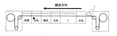
- FIG. 1 shows a schematic diagram of an example of the wet etching system of the present invention.
- the wet etching system of the present invention has an exposure means 1 and a wet etching means 2 as a basic configuration.
- the wet etching means 2 has an etchant composition tank, an etching tank, and an etchant composition discharge device (not shown).
- the wet etching means 2 includes a detection control device 3 and an etching component replenisher tank. 4 is connected.
- the detection control device 3 is supplied with the etchant composition from the wet etching means 2 through the liquid feed pipe 7 by the etchant composition liquid feed device 6.
- the detection control device 3 performs an analysis that is an index of the composition such as the oxidation-reduction potential, specific gravity, and pH of the etchant composition, and etches the control signal 10 so that the composition of the etchant composition falls within a predetermined range. It transmits to the component replenishment liquid feeding device 5.
- the etching component replenishing liquid feeding device 5 supplies the etching component replenishing liquid from the etching component replenishing liquid tank 4 to the wet etching means 2 through the liquid feeding pipe 9 in accordance with the received signal. Further, the etching agent composition analyzed by the detection control device 3 is returned to the wet etching means 2 through the liquid feeding pipe 8.
- the copper-containing material on the surface of which a positive photosensitive resist pattern, which is an object to be wet etched is sequentially passed through the exposure means 1 and the wet etching means 2 according to the transport route 11. It is conveyed to the next process.
- the transport means is not particularly limited, and for example, various conveyors, robot arms, and loaders / unloaders can be used.
- the thickness corresponding to the processing size of TapeBGA, TCP, and COF is 1 to 20 ⁇ m, and the etching space 1 It can be applied to patterning of ⁇ 20 ⁇ m.
- the wet etching system of the present invention is suitable for manufacturing a COF tape having a thickness of 1 to 10 ⁇ m and an etching space of 1 to 10 ⁇ m.
- FIG. 2 shows a schematic diagram of an example of the wet etching system of the present invention suitable for manufacturing these.
- FIG. 2 shows a roll-to-roll wet etching system. Note that the configurations 3 to 10 in FIG. 1 may be added to the wet etching system.
- the light source of the exposure means 1 in the wet etching system of the present invention is not particularly limited, and a light source similar to a general photolithography light source can be used.
- a light source fluorescent lamp, CRT, xenon lamp, tungsten lamp, carbon arc lamp, LED, metal halide lamp, ultra high pressure mercury lamp, nitrogen laser, argon ion laser, helium cadmium laser, helium neon laser, krypton ion laser, YAG A laser, an excimer laser, a semiconductor laser, etc. are mentioned.
- the radiation to be irradiated is not particularly limited as long as it is in the UV region, and examples thereof include i-line, h-line, and g-line.
- Embodiment 2 The copper-containing material patterning method of the present invention is such that after exposing a copper-containing material having a positive photosensitive resist pattern (resist image) formed on the surface thereof, wet etching is performed using a predetermined etchant composition. Do. According to this method, the resist image that has been altered by exposure can protect the upper corners of the circuit wiring during wet etching, suppress the narrowing of the upper width of the circuit wiring, and suppress the shape defect of the circuit pattern. it can.
- the exposure method is the same as that of general photolithography and is as described above.
- the etchant composition used for wet etching includes (A) at least one oxidant component selected from cupric ions and ferric ions (hereinafter referred to as “component (A)”), and (B) ethylene. It consists of an aqueous solution containing a compound (hereinafter referred to as “component (B)”) obtained by adding at least one selected from oxide and propylene oxide to active hydrogen of a (poly) amine compound.
- the component (A) is a component having a function of oxidizing a copper-containing material and performing etching, and cupric ions and ferric ions can be used alone or as a mixture thereof. These cupric ions and ferric ions can be contained in the etching composition by blending copper, a copper (II) compound and an iron (III) compound, respectively, as a supply source.
- the copper (II) compound include copper (II) chloride, copper (II) bromide, copper (II) sulfate, and copper (II) hydroxide.
- iron (III) compound examples include iron chloride (III), iron bromide (III), iron (III) iodide, iron (III) sulfate, iron (III) nitrate, and iron (III) acetate. Etc. These compounds can be used individually or in mixture of 2 or more types. Also, among these cupric ion or ferric ion supply sources, copper, copper chloride (II), copper sulfate (II) from the viewpoints of cost, stability of the etching agent composition, and controllability of the etching rate. ) And iron (III) chloride are preferred, and copper, copper (II) sulfate and iron (III) chloride are more preferred.
- the concentration of the component (A) in the etching agent composition is 0.1 to 15% by mass, preferably 1 to 10% by mass in terms of ions.
- ion conversion means cupric ion conversion or ferric ion conversion when using cupric ion or ferric ion alone, and includes cupric ion and ferric ion. When mixed and used, it means ion conversion of both cupric ions and ferric ions.
- concentration of the component (A) is less than 0.1% by mass, the etching time becomes long, so that the resist deteriorates and the productivity decreases. On the other hand, if the concentration of the component (A) exceeds 15% by mass, the etching rate cannot be controlled, and it becomes difficult to maintain the top width.
- the component (B) is a compound obtained by adding at least one selected from ethylene oxide and propylene oxide to active hydrogen of a (poly) amine compound.
- the (poly) amine compounds constituting this compound include monoethanolamine, diethanolamine, triethanolamine, monoisopropanolamine, diisopropanolamine, triisopropanolamine, ethanolisopropanolamine, diethanolisopropanolamine, and ethanoldiisopropanol.
- alkanolamines such as amines; alkylalkanolamines obtained by alkyl-substituting these alkanolamines; and compounds represented by the following general formula (1).
- R 1 represents an alkylene group having 2 to 6 carbon atoms
- X 1 to X 4 are a hydrogen atom or an alkyl group having 1 to 4 carbon atoms
- X 1 to X 4 At least one is hydrogen and n is a number from 0 to 5.
- examples of the alkyl group represented by X 1 to X 4 include methyl, ethyl, propyl, isopropyl, butyl, isobutyl, sec-butyl and tert-butyl.
- Examples of the alkylene group for R 1 include ethylene, propylene, butylene, butylene, pentylene, pentylene, and hexylene.
- ethylene oxide and propylene oxide may be block addition or random addition.
- (B) component can be used individually or in mixture of 2 or more types.
- the component (B) is preferably a compound represented by the following general formula (2), which is most excellent in maintaining the top width.
- R 1 represents an alkylene group having 2 to 6 carbon atoms
- X 5 to X 7 represent a group represented by the following general formula (3)
- X 8 represents a hydrogen atom or The group represented by the following general formula (3) is represented
- n represents a number of 1 to 5.
- R 2 and R 3 represent an ethylene group or a propylene group
- p and q represent a number with which the number average molecular weight of the compound is 200 to 10,000.
- R 2 is a propylene group and R 3 is an ethylene group because the effect of maintaining the top width is remarkable
- n is 1, and all of X 5 to X 8 are represented by the general formula (3
- the compound of the general formula (2) represented by) is preferable because it is easily available.
- the number average molecular weight of the component (B) is less than 200, a sufficient improvement in circuit shape may not be obtained. If the number average molecular weight is greater than 10,000, a sufficient etching rate cannot be obtained. May be insufficient. Therefore, the number average molecular weight of the component (B) is preferably 200 to 10,000. In particular, it is most preferable that the number average molecular weight of the component (B) is 200 to 5,000 because the etching rate is good.
- the concentration of the component (B) in the etching agent composition is 0.001 to 5% by mass, preferably 0.05 to 2% by mass.
- concentration of the component (B) is lower than 0.001% by mass, a sufficient use effect cannot be obtained.
- concentration of the component (B) is higher than 5 mass, a pattern shape defect or the like due to penetration into the resist interface occurs.
- Etching agent composition may contain the well-known component contained in an etching agent composition other than the said (A) component and (B) component.
- Well-known components include, for example, inorganic acids, organic acids, glycol ether compounds, surfactants, amino acid compounds, azole compounds, pyrimidine compounds, thiourea compounds, amine compounds, alkylpyrrolidone compounds, organic Chelating agent compounds, polyacrylamide compounds, hydrogen peroxide, persulfates, inorganic salts, cuprous ions, and ferrous ions.
- concentration when these known components are used is not particularly limited, but is generally in the range of 0.001% by mass to 10% by mass.
- Inorganic acids have the function of removing the copper oxide film and copper chloride on the surface of the copper-containing material to be etched, the function of stabilizing the oxidizer, and the function of improving the leveling property for the copper-containing material, thereby promoting the etching. It is an ingredient to do.
- the inorganic acid include nitric acid, hydrogen chloride, sulfuric acid, phosphoric acid, and polyphosphoric acid. These can be used individually or in mixture of 2 or more types.
- hydrogen chloride is preferable because etching control is easy.
- Phosphoric acid is also preferable because it has an effect of promoting etching of the Ni—Cr seed layer on the copper back surface.
- the concentration of the inorganic acid is preferably 0.05 to 10% by mass. If the concentration of the inorganic acid is lower than 0.05% by mass, a sufficient use effect may not be obtained. On the other hand, if the concentration of the inorganic acid is higher than 10% by mass, the etching becomes excessive and the etching rate cannot be controlled, and the circuit wiring may have a defective shape.
- organic acids include formic acid, acetic acid, propionic acid, butyric acid, valeric acid, caproic acid, acrylic acid, crotonic acid, isocrotonic acid, oxalic acid, malonic acid, succinic acid, glutaric acid, adipic acid, pimelic acid, maleic acid Carboxylic acids such as acids, fumaric acid, malic acid, tartaric acid, citric acid, glycolic acid, lactic acid, sulfamic acid, nicotinic acid, ascorbic acid, hydroxypivalic acid, levulinic acid and ⁇ -chloropropionic acid; and methanesulfonic acid, ethane Examples thereof include organic sulfonic acids such as sulfonic acid, 2-hydroxyethanesulfonic acid, propanesulfonic acid, benzenesulfonic acid and toluenesulfonic acid. These can be used individually or in mixture of 2 or more types.
- glycol ether compound examples include ethylene glycol monomethyl ether, ethylene glycol monoethyl ether, ethylene glycol monobutyl ether, diethylene glycol monomethyl ether, diethylene glycol monoethyl ether, diethylene glycol monobutyl ether, triethylene glycol monomethyl ether, triethylene glycol mono Ethyl ether, triethylene glycol monobutyl ether, propylene glycol monomethyl ether, propylene glycol monoethyl ether, propylene glycol monobutyl ether, dipropylene glycol monomethyl ether, dipropylene glycol monoethyl ether, dipropylene glycol monobutyl ether, tripropylene Low molecular glycol ether compounds such as recall monomethyl ether, tripropylene glycol monoethyl ether and 3-methyl-3-methoxy-3-methoxybutanol; and high such as polyethylene glycol monomethyl ether, polyethylene glycol monoethyl ether and
- the surfactant examples include an anionic surfactant, a nonionic surfactant other than the component (B), a cationic surfactant, and an amphoteric surfactant.
- the anionic surfactant include higher fatty acid salts, higher alcohol sulfate esters, sulfurized olefin salts, higher alkyl sulfonates, ⁇ -olefin sulfonates, sulfated fatty acid salts, sulfonated fatty acid salts, and phosphate esters.
- Nonionic surfactants include, for example, polyoxyalkylene alkyl ether, polyoxyalkylene alkenyl ether, polyoxyethylene polyoxypropylene alkyl ether (addition form of ethylene oxide and propylene oxide may be random or block) ), Polyethylene glycol propylene oxide adduct, polypropylene glycol ethylene oxide adduct, glycerin fatty acid ester or its ethylene oxide adduct, sorbitan fatty acid ester, polyoxyethylene sorbitan fatty acid ester, alkyl polyglucoside, fatty acid monoethanolamide or its ethylene oxide addition , Fatty acid-N-methylmonoethanolamide or its ethylene oxide adduct, fatty acid dietano Ruamido or an ethylene oxide adduct, a sucrose fatty acid ester, alkyl (poly) glycerol ether, polyglycerol fatty acid esters, polyethylene glycol fatty acid esters, fatty acid methyl este
- Examples of the cationic surfactant include alkyl (alkenyl) trimethyl ammonium salt, dialkyl (alkenyl) dimethyl ammonium salt, alkyl (alkenyl) quaternary ammonium salt, mono- or dialkyl (ether group, ester group or amide group).
- Alkenyl) quaternary ammonium salt alkyl (alkenyl) pyridinium salt, alkyl (alkenyl) dimethylbenzyl ammonium salt, alkyl (alkenyl) isoquinolinium salt, dialkyl (alkenyl) morphonium salt, polyoxyethylene alkyl (alkenyl) amine, alkyl (alkenyl) Examples thereof include amine salts, polyamine fatty acid derivatives, amyl alcohol fatty acid derivatives, benzalkonium chloride, and benzethonium chloride.
- amphoteric surfactant examples include carboxybetaine, sulfobetaine, phosphobetaine, amide amino acid, and imidazolinium betaine surfactant. Said surfactant can be used individually or in mixture of 2 or more types.
- amino acid compounds include amino acids such as glycine, alanine, valine, leucine, serine, phenylalanine, tryptophan, glutamic acid, aspartic acid, lysine, arginine, and histidine, and alkali metal salts and ammonium salts thereof. These can be used individually or in mixture of 2 or more types.
- azole compounds include alkyl imidazoles such as imidazole, 2-methylimidazole, 2-undecyl-4-methylimidazole, 2-phenylimidazole, 2-methylbenzimidazole; benzimidazole, 2-methylbenzimidazole, 2 -Benzimidazoles such as undecylbenzimidazole, 2-phenylbenzimidazole, 2-mercaptobenzimidazole; 1,2,3-triazole, 1,2,4-triazole, 5-phenyl-1,2,4-triazole 5-amino-1,2,4-triazole, 1,2,3-benzotriazole, 1-aminobenzotriazole, 4-aminobenzotriazole, 1-bisaminomethylbenzotriazole, 1-methyl-benzotriazole, Triazoles such as lutriazole, 1-hydroxybenzotriazole, 5-methyl-1H-benzotriazole, 5-chlorobenzotriazole; 1H-tetrazol
- Tetrazoles Tetrazoles; benzothiazole, 2-mercaptobenzothiazole, 2-phenylthiazole, 2-aminobenzothiazole, 2-amino-6-nitrobenzothiazole, 2-amino-6-methoxybenzothiazole, 2-amino-6-chlorobenzothi Thiazoles, such as tetrazole and the like. These can be used individually or in mixture of 2 or more types.
- pyrimidine compounds include diaminopyrimidine, triaminopyrimidine, tetraaminopyrimidine, and mercaptopyrimidine. These can be used alone or in combination.
- thiourea compound examples include thiourea, ethylenethiourea, thiodiglycol, and mercaptan. These can be used individually or in mixture of 2 or more types.
- amine compounds include diamylamine, dibutylamine, triethylamine, triamylamine, monoethanolamine, diethanolamine, triethanolamine, monoisopropanolamine, diisopropanolamine, triisopropanolamine, ethanolisopropanolamine, diethanolisopropanolamine, ethanol
- examples thereof include diisopropanolamine, polyallylamine, polyvinylpyridine, and hydrochlorides thereof. These can be used individually or in mixture of 2 or more types.
- Alkyl pyrrolidone compounds include N-methyl-2-pyrrolidone, N-ethyl-2-pyrrolidone, N-propyl-2-pyrrolidone, N-butyl-2-pyrrolidone, N-amyl-2-pyrrolidone, N-hexyl. Examples include -2-pyrrolidone, N-heptyl-2-pyrrolidone, and N-octyl-2-pyrrolidone. These can be used individually or in mixture of 2 or more types.
- organic chelating agent compound examples include ethylenediaminetetraacetic acid, diethylenetriaminepentaacetic acid, triethylenetetraminehexaacetic acid, tetraethylenepentaminepentaacetic acid, pentaethylenehexamineoctacetic acid, nitrilotriacetic acid, and alkali metal salts and ammonium salts thereof. Is mentioned. These can be used individually or in mixture of 2 or more types.
- polyacrylamide compounds examples include polyacrylamide and t-butylacrylamide sulfonic acid. These can be used individually or in mixture of 2 or more types.
- persulfate examples include ammonium persulfate, sodium persulfate, and potassium persulfate. These can be used individually or in mixture of 2 or more types.
- the inorganic salt examples include sodium chloride, potassium chloride, ammonium chloride, ammonium hydrogen carbonate, sodium hydrogen carbonate, potassium hydrogen carbonate, ammonium carbonate, sodium carbonate, potassium carbonate, ammonium sulfate, sodium sulfate, potassium sulfate, sodium nitrate, potassium nitrate, Examples thereof include ammonium nitrate, ammonium chlorate, sodium chlorate, and potassium chlorate. These can be used individually or in mixture of 2 or more types.
- cuprous ions examples include cuprous chloride, cuprous bromide, cuprous sulfate, and cuprous hydroxide.
- cuprous ions examples include cuprous chloride, cuprous bromide, cuprous sulfate, and cuprous hydroxide.
- ferrous ions examples include ferrous chloride, ferrous bromide, ferrous iodide, ferrous sulfate, ferrous nitrate, and ferrous acetate. These can be used individually or in mixture of 2 or more types.
- the etching agent composition can be prepared by mixing the above components and water.
- the mixing method is not particularly limited, and mixing may be performed using a known mixing device.
- Etching of the copper-containing material using the above-described etchant composition in the patterning method of the present invention can be performed by a well-known general method.
- the copper-containing material that is the material to be etched include copper alloys such as silver-copper alloys and aluminum-copper alloys, and copper, with copper being particularly preferred.
- the etching method is not particularly limited, and an immersion method, a spray method, or the like can be used. The etching conditions may be appropriately adjusted according to the etching agent composition to be used and the etching method.
- various known methods such as a batch method, a flow method, an oxidation-reduction potential or specific gravity of an etchant, and an auto-control method based on an acid concentration may be used.
- Various conditions for performing wet etching are not particularly limited, and may be set as appropriate in accordance with the type of the etchant composition to be used.
- the wet etching processing temperature is 30 to 50 ° C.
- the processing pressure is 0.05 to 0.2 MPa
- the processing time is 20 to 300 seconds. preferable.
- a replenisher may be added to the etchant composition used for wet etching in order to recover the deterioration of the liquid due to repeated wet etching.
- the replenisher is set in advance in the etching system and added to the etchant composition.
- the replenisher is, for example, the component (A), the component (B), the inorganic acid component, and water.
- concentrations of the component (A) and the inorganic acid are the same as those in the etchant composition used for wet etching. It is about 1 to 20 times.
- the positive photosensitive resist pattern is removed.
- the resist pattern may be removed using an appropriate resist remover depending on the type of positive photosensitive resist.
- the resist remover the same resist remover used in photolithography can be used.
- the resist remover include an alkaline aqueous solution remover.
- the alkaline component of the alkaline aqueous solution remover include sodium hydroxide, potassium hydroxide, sodium hydrogen carbonate, potassium hydrogen carbonate, sodium carbonate, and potassium carbonate.
- the alkaline aqueous solution remover may contain various organic amines, hydrazine, organic solvents, surfactants and the like as auxiliary agents and additives.
- the method for patterning a copper-containing material of the present invention as described above can form a fine circuit pattern without a shape defect, it can be used in various manufacturing applications such as a printed wiring board, a package substrate, a COF tape, and a TAB. Can be used.
- Examples 1-1 to 1-5, Comparative Examples 1-1 to 1-11 A novolak positive photosensitive resist (PMER-P; manufactured by Tokyo Ohka Kogyo Co., Ltd.) is applied to a COF tape base material (50 mm ⁇ 50 mm) with a copper thickness of 8 ⁇ m, dried, and then exposed to exposure equipment (UFX-2458B; USHIO) The resist pattern having a pitch of 25 ⁇ m and a space of 6 ⁇ m was formed by performing exposure and development and rinsing. Next, the COF tape base material on which the resist pattern was formed was subjected to an exposure process under the exposure conditions shown in Table 3 using an exposure apparatus (ultra-high pressure mercury lamp).
- PMER-P novolak positive photosensitive resist
- wet etching was performed by spraying for the number of seconds (60 to 100 seconds) for just etching using the above-mentioned etching composition under the conditions of a processing temperature of 45 ° C. and a processing pressure of 0.05 MPa. Then, the resist pattern was removed using a resist remover (acetone) to obtain a copper circuit pattern. The following evaluation was performed about the shape of the obtained copper circuit pattern.
- Examples 1-1 to 1-5 which were wet-etched using the etching agent compositions a to e containing 1 to 5, the reduction in the top width was small and the etching factor was improved.
- Examples 1-1 to 1-4 which were wet-etched using the etching composition a to d, had a smaller top width than Examples 1-5, which were wet-etched using the etching composition e.
- the etching factor was greatly improved.
- Comparative Examples 1-1 to 1-5 which were wet-etched without exposure, could not sufficiently suppress the reduction of the top width, and the etching factor was reduced.
- Comparative Examples 1-6 to 1-11 which were wet-etched using the etching agent compositions f to h, could not sufficiently suppress the reduction of the top width regardless of the presence or absence of exposure, and the etching factor was lowered. .
- Examples 2-1 to 2-5 Comparative Examples 2-1 to 2-5)
- a novolak positive photosensitive resist (PMER-P; manufactured by Tokyo Ohka Kogyo Co., Ltd.) is applied to a COF tape base material (50 mm ⁇ 50 mm) with a copper thickness of 8 ⁇ m, dried, and then exposed to exposure equipment (UFX-2458B; USHIO)
- the resist pattern having the pitches and spaces shown in Table 5 was formed by performing exposure and development and rinsing.
- the COF tape base material on which the resist pattern was formed was subjected to an exposure process under the exposure conditions shown in Table 5 using an exposure apparatus (ultra-high pressure mercury lamp).
- wet etching was performed by spraying for 90 seconds under the conditions of a processing temperature of 45 ° C. and a processing pressure of 0.05 MPa using the etching agent composition d. Then, the resist pattern was removed using a resist remover (acetone) to obtain a copper circuit pattern. With respect to the shape of the obtained copper circuit pattern, the above evaluations (1) to (3) were performed.
Landscapes
- Chemical & Material Sciences (AREA)
- Engineering & Computer Science (AREA)
- Chemical Kinetics & Catalysis (AREA)
- General Chemical & Material Sciences (AREA)
- Materials Engineering (AREA)
- Mechanical Engineering (AREA)
- Metallurgy (AREA)
- Organic Chemistry (AREA)
- Manufacturing & Machinery (AREA)
- Microelectronics & Electronic Packaging (AREA)
- ing And Chemical Polishing (AREA)
- Manufacturing Of Printed Circuit Boards (AREA)
Abstract
Description
高密度の回路配線を形成する方法としては、サブトラクティブ法やセミアディティブ法と呼ばれる方法が知られており、これらの方法ではウエットエッチングが行われている。
例えば、特許文献1には、酸化剤である2価鉄イオン、塩酸、銅含有材料エッチング促進剤、及び銅含有材料エッチング抑制剤を必須成分とするエッチング剤組成物を用いたセミアディティブ法による回路パターン形成方法が開示されている。ここで、銅含有材料エッチング抑制剤としては、アミン類化合物の活性水素基にプロピレンオキシド及びエチレンオキシドを付加した化合物が開示されており、銅表面の清浄化効果やレベリング性を向上させる成分としてリン酸を使用することも開示されている。
また、本発明は、ポジ型感光性レジストのパターンが表面に形成された銅含有材料を露光した後、(A)第二銅イオン及び第二鉄イオンから選択される少なくとも1つの酸化剤成分0.1~15質量%、及び(B)エチレンオキサイド及びプロピレンオキサイドから選択される少なくとも1つを(ポリ)アミン類化合物の活性水素に付加した化合物0.001~5質量%を含む水溶液からなるエッチング剤組成物を用いてウエットエッチングすることを特徴とする銅含有材料のパターニング方法である。
本発明のウエットエッチングシステムは、所定の銅含有材料を露光する露光手段と、当該露光手段により露光された銅含有材料をウエットエッチングする手段とを有する。
このウエットエッチングシステムに供給される銅含有材料は、ポジ型感光性レジストを用いたフォトリソグラフィーによって所望のパターン(レジスト像)が形成されたものである。ここで、フォトリソグラフィーは、当該技術分野において公知であり、露光及び現像によって所望のパターンを形成する技術である。このフォトリソグラフィーによる所望のパターンの形成は、公知の方法に準じて行なうことができる。なお、このフォトリソグラフィーにおける露光手段は、本発明のウエットエッチングシステムにおける露光手段と区別される。
本発明のウエットエッチングシステムは、露光手段と、エッチング剤組成物タンク、エッチング槽及びエッチング剤組成物吐出装置を有するウエットエッチング手段とを基本構成とし、ポジ型感光性レジストのパターンを除去する手段をウエットエッチング手段の後に設けることができる。また、これらの手段の前後に洗浄手段や乾燥手段を設けてもよく、エッチング処理対象物(銅含有材料)をエッチング槽に導入すると共にエッチング槽から取出す搬送手段を使用してもよい。さらに、ウエットエッチングの方式は、バッチ式及びフロー式のどちらでもよく、エッチング剤組成物の酸化還元電位、比重又はpHによるオートコントロールシステムを設けてもよい。なお、オートコントロールシステムを設ける場合は、エッチング剤組成物の組成をコントロールするための検出制御装置、及びエッチング成分補給液供給装置等を設ける必要がある。
これらの製造に適した本発明のウエットエッチングシステムの一例について、その概略図を図2に示す。図2は、ロールトゥロール方式のウエットエッチングシステムである。なお、当該ウエットエッチングシステムには、図1の3~10の構成を付加してもよい。
また、照射する放射線についても、UV領域のものであれば特に限定されず、例えば、i線、h線、g線が挙げられる。これらは、それぞれを選択的に照射しても、3線を含む輝線として照射してもよい。
さらに、照射する光量は、少な過ぎると充分な効果を得ることができず、多過ぎるとウエットエッチング処理時間が長くなることがあるので、10~400mJ/cm2が好ましく、50~250mJ/cm2がより好ましい。
本発明の銅含有材料のパターニング方法は、ポジ型感光性レジストのパターン(レジスト像)が表面に形成された銅含有材料を露光した後、所定のエッチング剤組成物を用いてウエットエッチングすることによって行なう。この方法によれば、露光によって変質したレジスト像が、ウエットエッチングの際に、回路配線の上部の角を保護して回路配線上部幅の細りを抑制し、回路パターンの形状不良を抑制することができる。
露光方法は、一般的なフォトリソグラフィーと同様であり、上述した通りである。
このエッチング剤組成物によって回路配線上部幅の細りが抑制される理由は明確ではないが、(B)成分がレジスト像に浸透して軟化を促進させ、回路配線上部の角を保護するか、又は(B)成分が銅含有材料とレジスト像との界面付近に特異的に局在化して部分的なエッチング抑制を行うことに起因していると考えられる。

エチレンオキサイドとプロプレンオキサイドの両方が(ポリ)アミン類化合物の活性水素に付加される場合、エチレンオキサイド及びプロピレンオキサイドは、ブロック付加でもよく、ランダム付加でもよい。また、(B)成分は、単独又は2種類以上を混合して用いることができる。


特に、R2がプロピレン基であり、R3がエチレン基であるものが、トップ幅の維持効果が顕著であるため好ましく、nが1であり、X5~X8の全てが一般式(3)で表される一般式(2)の化合物が入手容易であるため好ましい。
エッチング剤組成物に無機酸を配合する場合、無機酸の濃度は0.05~10質量%であることが好ましい。無機酸の濃度が0.05質量%よりも低いと、充分な使用効果を得ることができない場合がある。一方、無機酸の濃度が10質量%よりも高いと、エッチングが過剰となってエッチング速度の制御ができなくなり、回路配線の形状不良等が生じる場合がある。
アニオン性界面活性剤としては、例えば、高級脂肪酸塩、高級アルコール硫酸エステル塩、硫化オレフィン塩、高級アルキルスルホン酸塩、α-オレフィンスルホン酸塩、硫酸化脂肪酸塩、スルホン化脂肪酸塩、リン酸エステル塩、脂肪酸エステルの硫酸エステル塩、グリセライド硫酸エステル塩、脂肪酸エステルのスルホン酸塩、α-スルホ脂肪酸メチルエステル塩、ポリオキシアルキレンアルキルエーテル硫酸エステル塩、ポリオキシアルキレンアルキルフェニルエーテル硫酸エステル塩、ポリオキシアルキレンアルキルエーテルカルボン酸塩、アシル化ペプチド、脂肪酸アルカノールアミド又はそのアルキレンオキサイド付加物の硫酸エステル塩、スルホコハク酸エステル、アルキルベンゼンスルホン酸塩、アルキルナフタレンスルホン酸塩、アルキルベンゾイミダゾールスルホン酸塩、ポリオキシアルキレンスルホコハク酸塩、N-アシル-N-メチルタウリンの塩、N-アシルグルタミン酸又はその塩、アシルオキシエタンスルホン酸塩、アルコキシエタンスルホン酸塩、N-アシル-β-アラニン又はその塩、N-アシル-N-カルボキシエチルタウリン又はその塩、N-アシル-N-カルボキシメチルグリシン又はその塩、アシル乳酸塩、N-アシルサルコシン塩、及びアルキル又はアルケニルアミノカルボキシメチル硫酸塩等が挙げられる。
両性界面活性剤としては、例えば、カルボキシベタイン、スルホベタイン、ホスホベタイン、アミドアミノ酸、及びイミダゾリニウムベタイン系界面活性剤等が挙げられる。
上記の界面活性剤は、単独又は2種類以上を混合して用いることができる。
ウエットエッチングを行なう際の各種条件は、特に限定されず、使用するエッチング剤組成物の種類にあわせて適宜設定すればよい。上記のエッチング剤組成物を用いてスプレー法によりエッチングを行なう場合、ウエットエッチングの処理温度は30~50℃、処理圧力は0.05~0.2MPa、処理時間は20~300秒であることが好ましい。
(エッチング剤組成物の調製)
表1に記載の化合物と、4.9質量%の塩化第二鉄(第二鉄イオンの含有量:1.7質量%)と、6.6質量%の塩化第二銅(第二銅イオンの含有量:3.1質量%)と、0.2質量%の塩化水素と、0.94質量%のリン酸と、水とを配合することにより、エッチング剤組成物a~hを得た。エッチング剤組成物中の表1に記載の化合物の含有量については表2に示す。なお、エッチング剤組成物中の含有量の残部は水である。
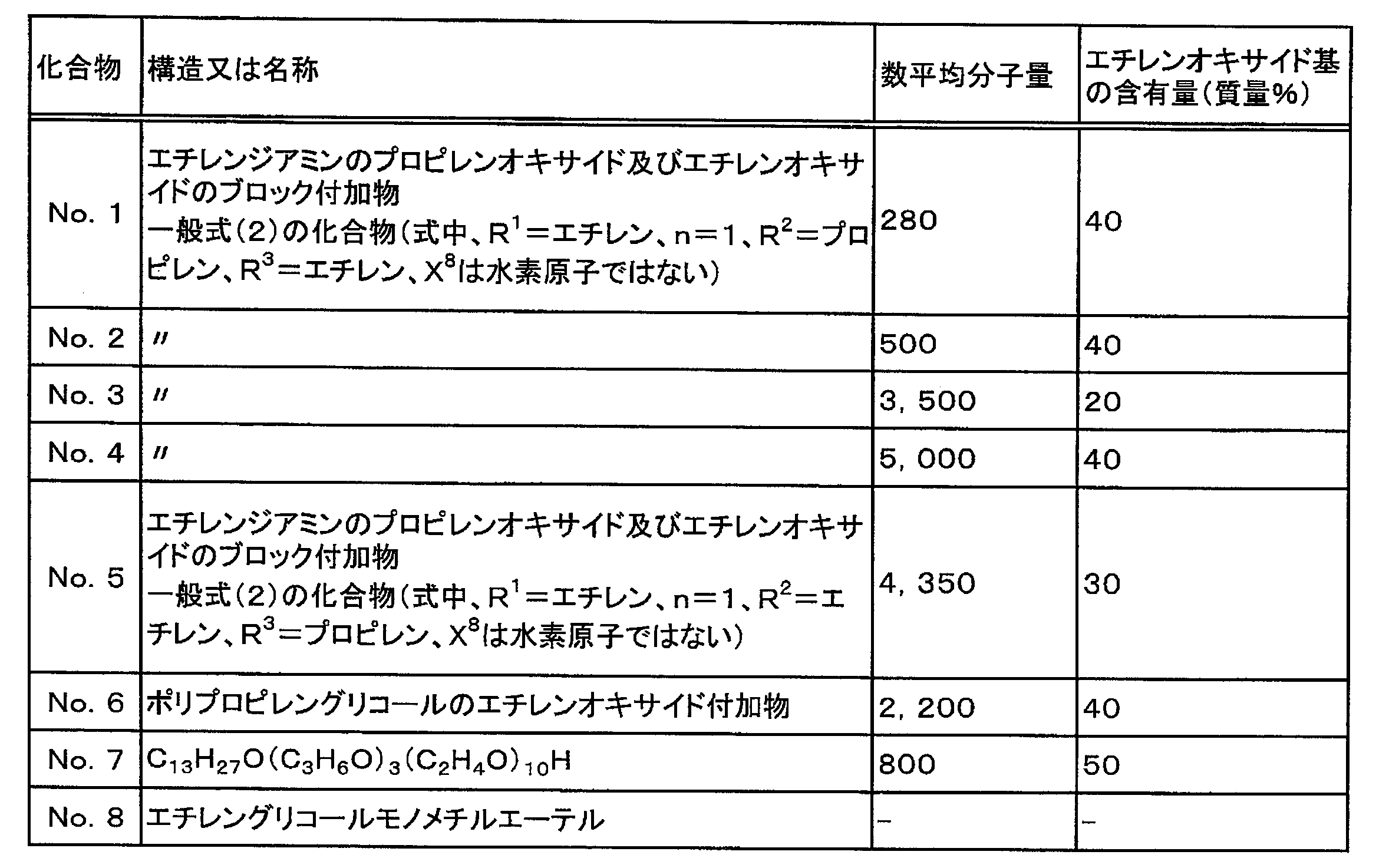
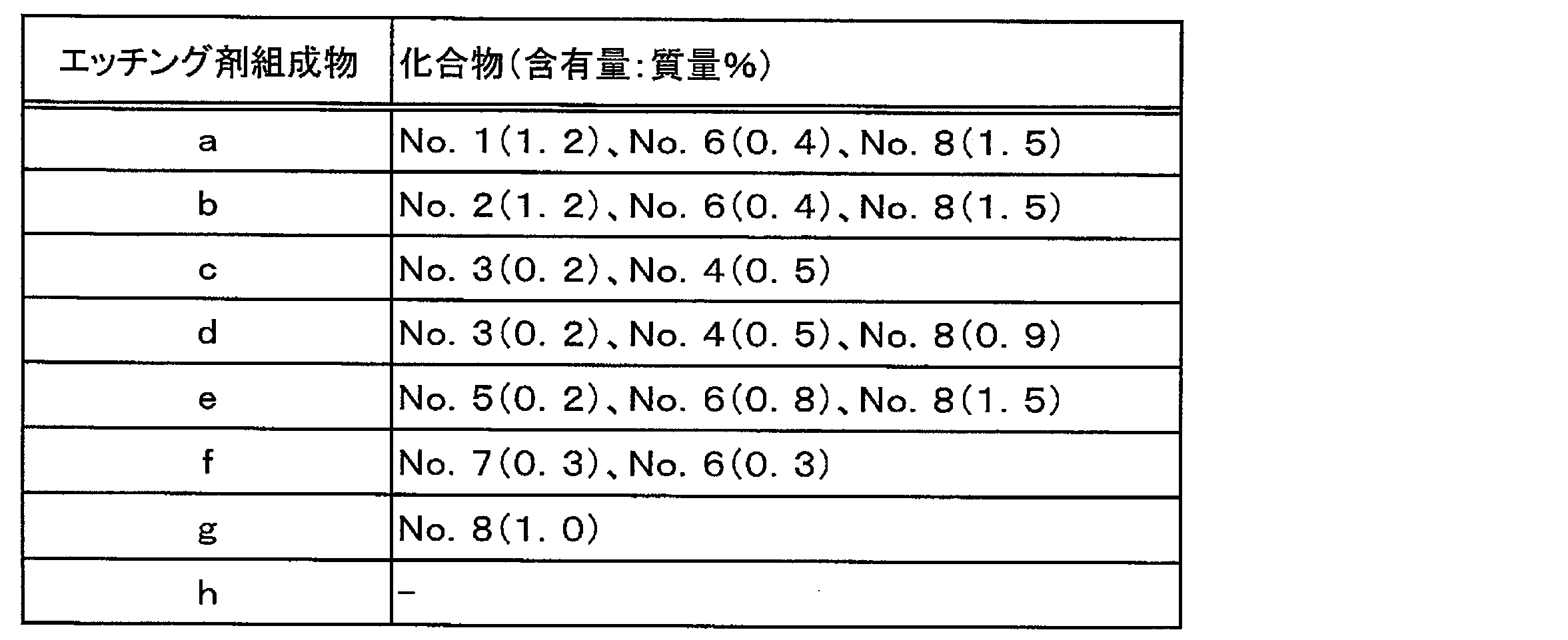
銅厚8μmのCOFテープ基材(50mmラ50mm)にノボラック系ポジ型感光性レジスト(PMER-P;東京応化株式会社製)を塗布して乾燥させた後、露光装置(UFX-2458B;ウシオ電機株式会社製)を用いて露光し、現像及びリンスを行うことにより、ピッチ25μm及びスペース6μmのレジストパターンを形成した。
次に、レジストパターンを形成したCOFテープ基材を、露光装置(超高圧水銀ランプ)を用い、表3に記載の露光条件で露光処理を行った。その後、上記のエッチング剤組成物を用い、処理温度45℃、処理圧力0.05MPaの条件下で、ジャストエッチングとなる秒数(60~100秒)の間スプレーすることでウエットエッチングを行なった。そして、レジスト除去剤(アセトン)を用いてレジストパターンを除去し、銅回路パターンを得た。得られた銅回路パターンの形状について、下記の評価を行なった。
レーザー顕微鏡像から測定した。単位はμmである。
(2)配線下部幅(ボトム幅)
レーザー顕微鏡像から測定した。単位はμmである。
(3)エッチングファクター
以下の式より算出した。
エッチングファクター=銅厚(μm)/{(B-T)/2}
式中、Tはトップ幅(μm)、Bはボトム幅(μm)である。
これらの評価結果について、表3及び4に示す。

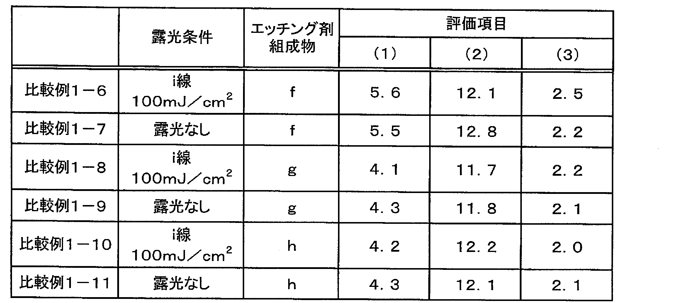
一方、露光を行なわずにウエットエッチングした比較例1-1~1~5は、トップ幅の減少を充分に抑制できず、エッチングファクターが低下した。また、エッチング剤組成物f~hを用いてウエットエッチングした比較例1-6~1-11は、露光の有無に関らず、トップ幅の減少を充分に抑制できず、エッチングファクターが低下した。
銅厚8μmのCOFテープ基材(50mmラ50mm)にノボラック系ポジ型感光性レジスト(PMER-P;東京応化株式会社製)を塗布して乾燥させた後、露光装置(UFX-2458B;ウシオ電機社製)を用いて露光し、次いで現像及びリンスを行うことにより、表5に記載のピッチ及びスペースを有するレジストパターンを形成した。
次に、レジストパターンを形成したCOFテープ基材を、露光装置(超高圧水銀ランプ)を用い、表5に記載の露光条件で露光処理を行った。その後、エッチング剤組成物dを用い、処理温度45℃、処理圧力0.05MPaの条件下で、90秒間スプレーすることでウエットエッチングを行なった。そして、レジスト除去剤(アセトン)を用いてレジストパターンを除去し、銅回路パターンを得た。得られた銅回路パターンの形状について、上記(1)~(3)の評価を行なった。
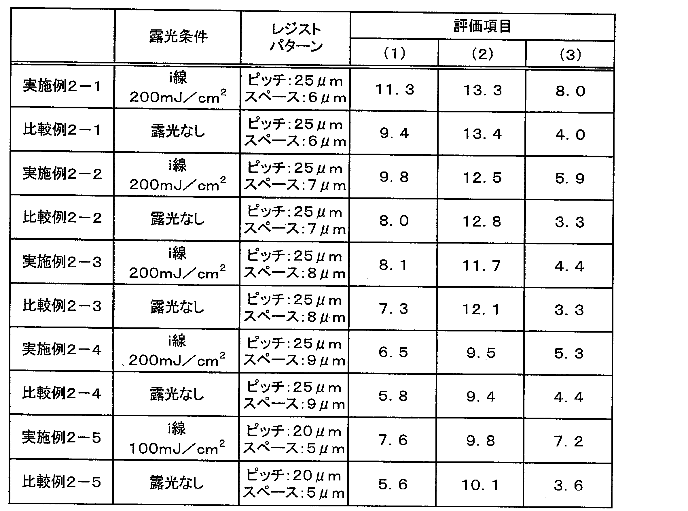
以上の結果からわかるように、本発明によれば、形状不良なしに(特に、回路配線上部幅を維持しつつ)微細な回路パターンを形成し得るウエットエッチングシステム及びパターニング方法を提供することができる。
Claims (2)
- ポジ型感光性レジストのパターンが表面に形成された銅含有材料を露光する露光手段と、
前記露光手段により露光された銅含有材料をウエットエッチングするウエットエッチング手段と
を有することを特徴とする銅含有材料のウエットエッチングシステム。 - ポジ型感光性レジストのパターンが表面に形成された銅含有材料を露光した後、(A)第二銅イオン及び第二鉄イオンから選択される少なくとも1つの酸化剤成分0.1~15質量%、及び(B)エチレンオキサイド及びプロピレンオキサイドから選択される少なくとも1つを(ポリ)アミン類化合物の活性水素に付加した化合物0.001~5質量%を含む水溶液からなるエッチング剤組成物を用いてウエットエッチングすることを特徴とする銅含有材料のパターニング方法。
Priority Applications (1)
| Application Number | Priority Date | Filing Date | Title |
|---|---|---|---|
| CN2010800273140A CN102471897A (zh) | 2009-07-09 | 2010-07-05 | 含铜材料的湿式蚀刻系统和图案化方法 |
Applications Claiming Priority (2)
| Application Number | Priority Date | Filing Date | Title |
|---|---|---|---|
| JP2009162713A JP2011017052A (ja) | 2009-07-09 | 2009-07-09 | 銅含有材料のウエットエッチングシステム及びパターニング方法 |
| JP2009-162713 | 2009-07-09 |
Publications (1)
| Publication Number | Publication Date |
|---|---|
| WO2011004789A1 true WO2011004789A1 (ja) | 2011-01-13 |
Family
ID=43429213
Family Applications (1)
| Application Number | Title | Priority Date | Filing Date |
|---|---|---|---|
| PCT/JP2010/061397 Ceased WO2011004789A1 (ja) | 2009-07-09 | 2010-07-05 | 銅含有材料のウエットエッチングシステム及びパターニング方法 |
Country Status (5)
| Country | Link |
|---|---|
| JP (1) | JP2011017052A (ja) |
| KR (1) | KR20120049177A (ja) |
| CN (1) | CN102471897A (ja) |
| TW (1) | TW201126021A (ja) |
| WO (1) | WO2011004789A1 (ja) |
Cited By (5)
| Publication number | Priority date | Publication date | Assignee | Title |
|---|---|---|---|---|
| WO2012143467A2 (de) | 2011-04-19 | 2012-10-26 | Schott Solar Ag | Verfahren zur herstellung einer solarzelle |
| US9636691B2 (en) | 2012-11-16 | 2017-05-02 | Corning Incorporated | Integrated cyclone separation device |
| CN112595629A (zh) * | 2020-12-29 | 2021-04-02 | 江西超洋科技有限公司 | 一种药水实时分析装置 |
| CN114540818A (zh) * | 2022-02-15 | 2022-05-27 | 江西省科学院应用物理研究所 | 一种铜镁硅合金金相腐蚀剂及其金相组织显示方法 |
| CN118272811A (zh) * | 2024-06-03 | 2024-07-02 | 新恒汇电子股份有限公司 | 降低蚀刻侧蚀量的防侧蚀剂及其使用方法 |
Families Citing this family (12)
| Publication number | Priority date | Publication date | Assignee | Title |
|---|---|---|---|---|
| TW201250059A (en) * | 2011-03-08 | 2012-12-16 | Nagase Chemtex Corp | Etching liquid |
| KR101385284B1 (ko) * | 2012-06-12 | 2014-04-21 | 풍원화학(주) | 에칭액, 에칭액에 첨가되는 첨가제 및 에칭액을 사용하는 기판의 제조 방법 |
| KR102079658B1 (ko) * | 2013-04-05 | 2020-02-20 | 해성디에스 주식회사 | 구리 함유 금속막 식각액 조성물 및 이를 이용한 식각 방법 |
| JP6207248B2 (ja) * | 2013-06-17 | 2017-10-04 | 株式会社Adeka | エッチング液組成物及びエッチング方法 |
| KR101593110B1 (ko) * | 2013-11-21 | 2016-02-11 | 주식회사 익스톨 | 분해방지용 안정화제가 포함된 터치스크린패널용 식각액 조성물 |
| JP6164614B2 (ja) * | 2013-12-06 | 2017-07-19 | メック株式会社 | エッチング液、補給液及び銅配線の形成方法 |
| CN104278272B (zh) * | 2014-04-30 | 2017-09-08 | 天津普林电路股份有限公司 | 一种高密度互连电路板循环使用的酸性蚀刻液及其制备方法 |
| KR102209423B1 (ko) * | 2014-06-27 | 2021-01-29 | 동우 화인켐 주식회사 | 금속막의 식각액 조성물 및 이를 이용한 액정표시장치용 어레이 기판의 제조방법 |
| KR102020414B1 (ko) * | 2017-12-22 | 2019-09-10 | 주식회사 포스코 | 아연 전기도금 냉연강판의 무늬형 표면 결함 제거용 에칭 조성물 및 상기 에칭 조성물을 포함하는 산세 조성물 |
| KR102205628B1 (ko) * | 2019-02-12 | 2021-01-21 | 김진호 | 구리 또는 구리 함유 금속막 식각액 조성물 |
| US10978412B2 (en) * | 2019-07-30 | 2021-04-13 | Taiwan Semiconductor Manufacturing Company, Ltd. | Manufacturing method of package structure |
| JP7507041B2 (ja) * | 2020-08-25 | 2024-06-27 | 株式会社Adeka | 組成物、エッチング方法、及び回路パターン形成方法 |
Citations (3)
| Publication number | Priority date | Publication date | Assignee | Title |
|---|---|---|---|---|
| JPH06280052A (ja) * | 1993-03-26 | 1994-10-04 | Canon Inc | エッチング方法及び装置 |
| JP2003138389A (ja) * | 2001-10-30 | 2003-05-14 | Asahi Denka Kogyo Kk | エッチング剤組成物及びパターン形成方法 |
| JP2004256901A (ja) * | 2003-02-27 | 2004-09-16 | Mec Kk | 銅又は銅合金のエッチング液及びそれを用いる電子基板の製造方法 |
Family Cites Families (1)
| Publication number | Priority date | Publication date | Assignee | Title |
|---|---|---|---|---|
| CN1854343A (zh) * | 2005-04-26 | 2006-11-01 | 李德良 | 一种铜蚀刻液及其循环使用方法 |
-
2009
- 2009-07-09 JP JP2009162713A patent/JP2011017052A/ja not_active Withdrawn
-
2010
- 2010-07-05 KR KR1020117025466A patent/KR20120049177A/ko not_active Withdrawn
- 2010-07-05 WO PCT/JP2010/061397 patent/WO2011004789A1/ja not_active Ceased
- 2010-07-05 CN CN2010800273140A patent/CN102471897A/zh active Pending
- 2010-07-08 TW TW099122410A patent/TW201126021A/zh unknown
Patent Citations (3)
| Publication number | Priority date | Publication date | Assignee | Title |
|---|---|---|---|---|
| JPH06280052A (ja) * | 1993-03-26 | 1994-10-04 | Canon Inc | エッチング方法及び装置 |
| JP2003138389A (ja) * | 2001-10-30 | 2003-05-14 | Asahi Denka Kogyo Kk | エッチング剤組成物及びパターン形成方法 |
| JP2004256901A (ja) * | 2003-02-27 | 2004-09-16 | Mec Kk | 銅又は銅合金のエッチング液及びそれを用いる電子基板の製造方法 |
Cited By (6)
| Publication number | Priority date | Publication date | Assignee | Title |
|---|---|---|---|---|
| WO2012143467A2 (de) | 2011-04-19 | 2012-10-26 | Schott Solar Ag | Verfahren zur herstellung einer solarzelle |
| US9636691B2 (en) | 2012-11-16 | 2017-05-02 | Corning Incorporated | Integrated cyclone separation device |
| CN112595629A (zh) * | 2020-12-29 | 2021-04-02 | 江西超洋科技有限公司 | 一种药水实时分析装置 |
| CN114540818A (zh) * | 2022-02-15 | 2022-05-27 | 江西省科学院应用物理研究所 | 一种铜镁硅合金金相腐蚀剂及其金相组织显示方法 |
| CN114540818B (zh) * | 2022-02-15 | 2023-11-10 | 江西省科学院应用物理研究所 | 一种铜镁硅合金金相腐蚀剂及其金相组织显示方法 |
| CN118272811A (zh) * | 2024-06-03 | 2024-07-02 | 新恒汇电子股份有限公司 | 降低蚀刻侧蚀量的防侧蚀剂及其使用方法 |
Also Published As
| Publication number | Publication date |
|---|---|
| JP2011017052A (ja) | 2011-01-27 |
| CN102471897A (zh) | 2012-05-23 |
| TW201126021A (en) | 2011-08-01 |
| KR20120049177A (ko) | 2012-05-16 |
Similar Documents
| Publication | Publication Date | Title |
|---|---|---|
| JP2011017052A (ja) | 銅含有材料のウエットエッチングシステム及びパターニング方法 | |
| JP4916455B2 (ja) | 銅含有材料用エッチング剤組成物 | |
| JP4685180B2 (ja) | 銅含有材料用エッチング剤組成物及び銅含有材料のエッチング方法 | |
| JP5443863B2 (ja) | 銅含有材料用エッチング剤組成物及び銅含有材料のエッチング方法 | |
| JP5535060B2 (ja) | 銅含有材料用エッチング剤組成物及び銅含有材料のエッチング方法 | |
| CN1576395A (zh) | 蚀刻剂、补充液以及用它们制造铜布线的方法 | |
| EP2878706B1 (en) | Microetching agent for copper, supplementary liquid for same, and manufacturing method for circuit board | |
| JP2011233769A (ja) | 銅配線パターンの形成方法 | |
| JP2017171992A (ja) | 銀含有材料用エッチング液組成物及びエッチング方法 | |
| WO2021117478A1 (ja) | エッチング液組成物及びエッチング方法 | |
| US20120308929A1 (en) | Wet lamination of photopolymerizable dry films onto substrates and compositions relating thereto | |
| WO2018207479A1 (ja) | エッチング液組成物及びエッチング方法 | |
| KR102079658B1 (ko) | 구리 함유 금속막 식각액 조성물 및 이를 이용한 식각 방법 | |
| JP4431860B2 (ja) | 銅および銅合金の表面処理剤 | |
| CN105974735B (zh) | 阻焊剂图案的形成方法 | |
| JP4104109B2 (ja) | 半導体製造プロセス用ドライエッチング残渣除去液 | |
| HK1167876A (en) | Wet etching system for copper-containing material, and patterning method | |
| JP2017166043A (ja) | 銅含有材料用エッチング液組成物及び銅含有材料をエッチングする方法 | |
| WO2020080178A1 (ja) | エッチング液組成物及びエッチング方法 | |
| KR102124328B1 (ko) | 구리 금속 표면의 밀착 향상용 미세 조도 형성 조성물 | |
| CN112135927A (zh) | 组合物和蚀刻方法 | |
| KR20140122614A (ko) | 구리 함유 금속막 식각액 조성물 및 이를 이용한 식각 방법 | |
| JP2020097773A (ja) | バナジウム含有材料用エッチング液組成物及びエッチング方法 |
Legal Events
| Date | Code | Title | Description |
|---|---|---|---|
| WWE | Wipo information: entry into national phase |
Ref document number: 201080027314.0 Country of ref document: CN |
|
| 121 | Ep: the epo has been informed by wipo that ep was designated in this application |
Ref document number: 10797100 Country of ref document: EP Kind code of ref document: A1 |
|
| ENP | Entry into the national phase |
Ref document number: 20117025466 Country of ref document: KR Kind code of ref document: A |
|
| NENP | Non-entry into the national phase |
Ref country code: DE |
|
| 122 | Ep: pct application non-entry in european phase |
Ref document number: 10797100 Country of ref document: EP Kind code of ref document: A1 |