WO2010150786A1 - 電動機駆動装置の制御装置 - Google Patents
電動機駆動装置の制御装置 Download PDFInfo
- Publication number
- WO2010150786A1 WO2010150786A1 PCT/JP2010/060567 JP2010060567W WO2010150786A1 WO 2010150786 A1 WO2010150786 A1 WO 2010150786A1 JP 2010060567 W JP2010060567 W JP 2010060567W WO 2010150786 A1 WO2010150786 A1 WO 2010150786A1
- Authority
- WO
- WIPO (PCT)
- Prior art keywords
- control
- voltage
- system voltage
- rectangular wave
- change
- Prior art date
- Legal status (The legal status is an assumption and is not a legal conclusion. Google has not performed a legal analysis and makes no representation as to the accuracy of the status listed.)
- Ceased
Links
Images





Classifications
-
- H—ELECTRICITY
- H02—GENERATION; CONVERSION OR DISTRIBUTION OF ELECTRIC POWER
- H02P—CONTROL OR REGULATION OF ELECTRIC MOTORS, ELECTRIC GENERATORS OR DYNAMO-ELECTRIC CONVERTERS; CONTROLLING TRANSFORMERS, REACTORS OR CHOKE COILS
- H02P6/00—Arrangements for controlling synchronous motors or other dynamo-electric motors using electronic commutation dependent on the rotor position; Electronic commutators therefor
- H02P6/10—Arrangements for controlling torque ripple, e.g. providing reduced torque ripple
Definitions
- the present invention relates to an electric motor drive comprising: a system voltage generator that generates a DC system voltage; and a DC / AC converter that converts the system voltage into a plurality of phases of AC voltages that are out of phase with each other and supplies the AC voltage to an AC motor.
- the present invention relates to a control device that controls the device.
- An electric motor drive device that drives an AC motor by converting a DC voltage from a DC power source into an AC voltage by an inverter is generally used.
- PWM pulse width modulation
- maximum torque control based on vector control are performed in order to efficiently generate torque by supplying a sinusoidal AC voltage to the coils of each phase of the AC motor.
- the induced voltage increases as the rotational speed increases, and the AC voltage (hereinafter referred to as “required voltage”) required to drive the AC motor also increases.
- Patent Document 1 describes an electric motor drive device that includes a boost converter that boosts a power supply voltage from a DC power supply and can increase the system voltage.
- the control device that controls the motor drive device can increase the maximum output voltage by increasing the system voltage in accordance with the increase in necessary voltage, and can expand the maximum torque control region to a higher rotational speed region. Yes.
- the control device is configured to perform rectangular wave control according to field weakening control.
- the control device described in Patent Document 1 uses a rectangular wave after the system voltage becomes equal to the maximum system voltage boosted with respect to the power supply voltage, in other words, after the rotational speed of the AC motor becomes relatively high. It is configured to perform control.
- JP 2006-31770 A paragraphs 0046 to 0048, etc.
- the number of on / off operations of the switching elements constituting the inverter can be significantly reduced as compared with the PWM control, so that the switching loss can be suppressed. Therefore, in order to improve the efficiency of the electric motor drive device, it is conceivable to perform a rectangular wave control from a lower rotational speed range. However, if the system voltage is boosted during the execution of the rectangular wave control, the balance of the voltages supplied to the coils of each phase is lost, and a torque ripple is generated in which the output torque of the AC motor varies depending on the rotation angle.
- the system voltage is boosted during PWM control, and the rectangular wave control is performed after the system voltage becomes equal to the maximum system voltage boosted with respect to the power supply voltage. Therefore, the rectangular wave control is not performed until the system voltage is raised to the maximum system voltage, and the use area of the rectangular wave control with a small switching loss is limited to the high rotation speed range.
- a change in system voltage also occurs in an operating condition or system in which a DC voltage from a DC power source is supplied as it is without changing the active system voltage using a boost converter. That is, the output voltage of the DC power supply changes according to the discharge current or charging current of the DC power supply, and the system voltage changes accordingly. If the rectangular wave control is not performed while the system voltage is changing, torque ripple is prevented from being generated by the rectangular wave control, but the execution of the rectangular wave control with a small switching loss is limited. On the other hand, if the rectangular wave control is performed even while the system voltage is changing, the rectangular wave control with a small switching loss can be executed, but torque ripple may occur due to the rectangular wave control.
- the present invention has been made in view of the above-described problems, and the object of the present invention is to expand the use area of rectangular wave control with low switching loss to the low rotation speed region side, and the system voltage is reduced during rectangular wave control. Even if it changes, it is providing the control apparatus of the motor drive device which can suppress the vibration of an AC motor.
- the characteristic configuration of the control device that controls the electric motor drive device including the conversion unit is a rectangular wave control that performs on / off control of a plurality of switching elements provided in the DC / AC conversion unit and outputs a rectangular wave voltage of a plurality of phases.
- a switching control unit that performs a length of an integral multiple of an electrical angle round based on a rate of change of the system voltage when the system voltage changes during execution of the rectangular wave control. ON / OFF timing of the plurality of switching elements so that the time integral value of the rectangular wave voltage of each phase within the control cycle set to be substantially the same between the phases It lies in performing rectangular wave width adjustment control to set.
- the system voltage changes during execution of the rectangular wave control
- the voltage supplied to the coil of each phase within the control cycle set to a length that is an integral multiple of one round electrical angle Can be prevented from being lost, and the occurrence of torque ripple can be suppressed. Therefore, even when the system voltage is changing, the rectangular wave control can be performed while suppressing the vibration of the AC motor.
- the use area of rectangular wave control with little switching loss can be expanded, and the efficiency of the electric motor drive device can be increased.
- the system voltage can be changed while suppressing the vibration of the AC motor even during execution of the rectangular wave control.
- the rectangular wave control can be performed from a low rotation speed range where the system voltage is not boosted to the maximum system voltage. As a result, the use area of the rectangular wave control with little switching loss can be expanded to the low rotation speed area side, and the efficiency of the electric motor drive device can be increased.
- a point at which the voltage value of the rectangular wave voltage of each phase is switched between a high level and a low level by turning on and off the plurality of switching elements is set as a high / low switching point
- the switching control unit includes the control cycle A period set by dividing the control cycle with each of the high-low switching points of the rectangular wave voltage of a plurality of phases as a dividing point, and the rectangular wave width
- the adjustment control is based on the length of the control cycle, the value of the system voltage at the start point of the control cycle, and the rate of change of the system voltage within the control cycle, and the system voltage in each of the divided periods. Control for setting on / off timings of the plurality of switching elements so that the time integral values of the plurality of switching elements are substantially the same. To be suitable.
- the time integral value of the system voltage in each divided period is By simply setting the on / off timing of the switching elements so as to be substantially the same, the time integral values of the rectangular wave voltages of each phase within the control period can be made substantially the same. Therefore, the calculation required for the rectangular wave width adjustment control can be simplified, and the configuration of the control device can be simplified. It is also possible to prepare map data representing the correspondence relationship between the above three parameters and the on / off timing in advance, and obtain and set the on / off timing of a plurality of switching elements by referring to the map data. It is.
- the system voltage generation unit includes a voltage conversion unit that converts a power supply voltage from a DC power supply to generate a desired system voltage, and is a system voltage that is a command value of the system voltage generated by the voltage conversion unit
- a voltage conversion control unit that obtains a command value and performs on / off control of a switching element included in the voltage conversion unit based on the system voltage command value is further provided, and the voltage conversion control unit includes the voltage conversion unit.
- the change start timing for starting the change of the system voltage is made to coincide with any one of the on / off timings of the plurality of switching elements provided in the DC / AC converter, and the switching control unit It is preferable to make the start point of the cycle coincide with the change start timing.
- the rectangular wave width adjustment control can be performed from the initial time when the change of the system voltage is started, and the generation of torque ripple can be more reliably suppressed.
- the voltage conversion control unit sets a change end timing for ending the change of the system voltage as an integer of one round of electrical angle from the change start timing among the on / off timings of the plurality of switching elements included in the DC / AC conversion unit. It is preferable to match the on / off timing which is different in timing by twice.
- the rectangular wave width adjustment control can be performed in the entire period from the change start timing to the change end timing, and the occurrence of torque ripple can be more reliably suppressed.
- the system voltage is an output voltage of a DC power supply
- the rate of change of the system voltage is the value of the system voltage at the start point of the control cycle and the value of the system voltage past from the start point of the control cycle. It is preferable to calculate based on
- each phase within the control cycle is adapted to the change in the system voltage.
- the time integral value of the rectangular wave voltage can be made substantially the same. Therefore, even if an unexpected system voltage change occurs, the rectangular wave control can be performed while appropriately suppressing the vibration of the AC motor.
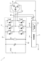
- the motor drive device 1 is a synchronous motor 4 (IPMSM, hereinafter simply referred to as “motor 4”) having an embedded magnet structure as an AC motor that operates by three-phase AC.
- IPMSM synchronous motor 4
- the electric motor 4 is configured to operate as a generator as required, and is used as a driving force source for, for example, an electric vehicle or a hybrid vehicle.
- the motor drive device 1 includes a system voltage generator 32 that generates a DC system voltage, and an inverter 6 that converts the system voltage Vdc into a three-phase AC voltage that is out of phase with each other and supplies the AC voltage to the motor 4.
- the system voltage generation unit 32 includes a DC power supply 3 and a converter 5 that converts the power supply voltage Vb from the DC power supply 3 to generate a desired system voltage Vdc.
- the control device 2 controls the electric motor drive device 1 using a vector control method, and controls on / off of the plurality of switching elements E3 to E8 included in the inverter 6 to provide a three-phase rectangular wave voltage. Is capable of executing rectangular wave control.
- the control device 2 performs the control set to the length of one round of the electrical angle based on the change rate K of the system voltage Vdc. It is characterized in that the rectangular wave width adjustment control for setting the on / off timing of the switching elements E3 to E8 is performed so that the time integral value of the rectangular wave voltage of each phase within the period T is substantially the same between the phases. .
- the electric motor drive device 1 and its control device 2 according to the present embodiment will be described in detail.
- the electric motor drive device 1 includes a converter 5 and an inverter 6.
- the electric motor drive device 1 includes a DC power source 3, a first smoothing capacitor C1 that smoothes the DC voltage Vb from the DC power source 3, and a second smoothing capacitor C2 that smoothes the system voltage Vdc boosted by the converter 5.
- the DC power source 3 for example, various secondary batteries such as a nickel hydride secondary battery and a lithium ion secondary battery, a capacitor, or a combination thereof is used.
- a power supply voltage Vb which is a voltage of the DC power supply 3, is detected by the power supply voltage sensor 41 and output to the control device 2.
- the converter 5 is a DC-DC converter that converts the power supply voltage Vb from the DC power supply 3 to generate a DC system voltage Vdc having a desired value, and corresponds to a voltage converter in the present invention.
- the converter 5 functions as a boost converter that boosts the power supply voltage Vb to generate a desired system voltage Vdc.
- the motor 4 functions as a generator
- the system voltage Vdc from the inverter 6 is stepped down and supplied to the DC power source 3 to charge the DC power source 3.
- the converter 5 includes a reactor L1, voltage conversion switching elements E1 and E2, and diodes D1 and D2.
- the converter 5 includes a pair of upper arm element E1 and lower arm element E2 connected in series as switching elements for voltage conversion.
- IGBTs insulated gate bipolar transistors
- the emitter of the upper arm element E1 and the collector of the lower arm element E2 are connected to the positive terminal of the DC power supply 3 via the reactor L1.
- the collector of the upper arm element E1 is connected to the system voltage line 51 to which the voltage boosted by the converter 5 is supplied, and the emitter of the lower arm element E2 is connected to the negative line 52 connected to the negative terminal of the DC power supply 3.
- diodes D1 and D2 that function as freewheeling diodes are connected in parallel to the voltage conversion switching elements E1 and E2, respectively.
- power transistors having various structures such as a bipolar type, a field effect type, and a MOS type can be used.
- Each of the voltage conversion switching elements E1 and E2 performs an on / off operation according to the switching control signals S1 and S2 output from the control device 2.
- the switching control signals S1 and S2 are gate drive signals that drive the gates of the switching elements E1 and E2.
- converter 5 boosts power supply voltage Vb supplied from DC power supply 3 to desired system voltage Vdc and supplies it to system voltage line 51 and inverter 6 during the boosting operation.
- Converter 5 steps down system voltage Vdc supplied from inverter 6 and supplies it to DC power supply 3 during the step-down operation.
- System voltage Vdc generated by converter 5 is detected by system voltage sensor 42 and output to control device 2.
- system voltage command value Vdct which is a system voltage command value, is equal to power supply voltage Vb and not boosted by converter 5
- system voltage Vdc is equal to power supply voltage Vb.
- the inverter 6 is a device for converting a DC system voltage Vdc into an AC voltage and supplying it to the electric motor 4, and corresponds to a DC / AC conversion unit in the present invention.
- the inverter 6 includes a plurality of sets of switching elements E3 to E8 and diodes D3 to D8.
- the inverter 6 is a pair of switching elements for each phase of the electric motor 4 (U-phase, V-phase, and W-phase), specifically, the U-phase upper arm element E3 and the U-phase lower An arm element E4, a V-phase upper arm element E5, a V-phase lower arm element E6, a W-phase upper arm element E7, and a W-phase lower arm element E8 are provided.
- IGBTs insulated gate bipolar transistors
- the emitters of the upper arm elements E3, E5, and E7 for each phase and the collectors of the lower arm elements E4, E6, and E8 are connected to the coils of the respective phases of the electric motor 4, respectively.
- the collectors of the upper arm elements E3, E5, E7 for each phase are connected to the system voltage line 51, and the emitters of the lower arm elements E4, E6, E8 for each phase are connected to the negative line 52.
- diodes D3 to D8 functioning as free wheel diodes are connected in parallel to the switching elements E3 to E8, respectively.
- power transistors having various structures such as a bipolar type, a field effect type, and a MOS type can be used in addition to the IGBT.
- Each of the switching elements E3 to E8 performs an on / off operation according to the switching control signals S3 to S8 output from the control device 2.
- the inverter 6 converts the system voltage Vdc into a three-phase AC voltage that is out of phase with each other, supplies the converted voltage to the electric motor 4, and causes the electric motor 4 to output a torque corresponding to the target torque TM.
- each of the switching elements E3 to E8 performs a switching operation according to PWM (pulse width modulation) control or rectangular wave control, which will be described later, according to the switching control signals S3 to S8.
- the switching control signals S3 to S8 are gate drive signals that drive the gates of the switching elements E3 to E8.
- the motor 4 when the motor 4 functions as a generator, the generated AC voltage is converted into a DC voltage and supplied to the system voltage line 51 and the converter 5.
- Each phase current flowing between the inverter 6 and each phase coil of the electric motor 4, specifically, the U-phase current Iur, the V-phase current Ivr, and the W-phase current Iwr is detected by the current sensor 43 and is controlled. 2 is output.
- the magnetic pole position ⁇ at each time point of the rotor of the electric motor 4 is detected by the rotation sensor 44 and output to the control device 2.
- the rotation sensor 44 is configured by, for example, a resolver.
- the magnetic pole position ⁇ represents the rotation angle of the rotor on the electrical angle.
- the target torque TM of the electric motor 4 and the system voltage command value Vdct are input to the control device 2 as request signals from other control devices such as a vehicle control device (not shown).
- the control device 2 includes a switching control unit 30 and a voltage conversion control unit 31.
- Each functional unit of the control device 2 is configured by hardware and / or software (program) or both for performing various processes on input data using a logic circuit such as a microcomputer as a core member.
- the switching control unit 30 generates switching control signals S3 to S8 for driving the electric motor 4 in accordance with the target torque TM, the magnetic pole position ⁇ , and the rotational speed ⁇ of the electric motor 4 derived from the magnetic pole position ⁇ . And output it to drive the inverter 6.
- the control device 2 drives the inverter 6 by switching between PWM control and maximum torque control, rectangular wave control and field weakening control. Further, the control device 2 receives the power supply voltage Vb of the DC power supply 3, the system voltage Vdc generated by the converter 5, and the system voltage command value Vdct. Therefore, voltage conversion control unit 31 generates and outputs switching control signals S1 and S2 for generating system voltage Vdc equal to input system voltage command value Vdct, and drives converter 5.
- the switching control unit 30 switches between PWM control and rectangular wave control when performing DC-AC conversion in the inverter 6.
- the PWM control includes two control methods, sine wave PWM control and overmodulation PWM control.
- sine wave PWM control on / off of each of the switching elements E3 to E8 of the inverter 6 is controlled based on a comparison between a sine wave voltage command value and a carrier wave.
- the output voltage waveform of the inverter 6 of each phase of U, V, W is a high level period in which the upper arm elements E3, E5, E7 are turned on, and the lower arm elements E4, E6, E8 are turned on.
- the duty ratio of each pulse is controlled so that the fundamental wave component becomes a sine wave in a certain period while being composed of a set of pulses composed of a low level period in which the state is entered. If the ratio of the effective value of the fundamental wave component of the output voltage waveform of the inverter 6 to the system voltage Vdc is the modulation factor m, the modulation factor m can be changed in the range of 0 to 0.61 in the sine wave PWM control. In this sine wave PWM control, for example, torque control can be performed by motor current control (motor current feedback control) according to vector control.
- overmodulation PWM control the switching control unit 30 reduces the duty ratio of each pulse on the peak side of the fundamental wave component and lower on the valley side compared to the sine wave PWM control, so that the fundamental wave component of the output voltage waveform of the inverter 6 is increased.
- the waveform is distorted to control the amplitude to be larger than the sine wave PWM control.
- the modulation factor m can be changed in the range of 0.61 to 0.78.
- the state where the modulation factor m is increased to the maximum 0.78 is the rectangular wave control.
- torque control can be performed by motor current control (motor current feedback control) according to vector control.
- the switching control unit 30 causes the output voltage waveform of the inverter 6 of each phase of U, V, and W to alternately appear between a high level period and a low level period once per cycle. Control is performed so that the ratio of the level period to the low level period is basically a rectangular wave of 1: 1. Thus, the rectangular wave control causes the inverter 6 to output a rectangular wave voltage.
- the switching control unit 30 is a control unit that performs on / off control of the plurality of switching elements E3 to E8 provided in the inverter 6 and performs rectangular wave control for outputting a three-phase rectangular wave voltage.
- the modulation factor m is fixed at 0.78.
- the actual torque value obtained by power calculation based on the current values Iur, Ivr, Iwr and voltage command values of the U, V, W phases detected by the current sensor 43, and the torque command Torque control can be performed by voltage phase control (torque feedback control) based on the deviation from the value. Further, torque control can be performed by motor current control (motor current feedback control) according to vector control.
- torque control can be performed by motor current control (motor current feedback control) according to vector control.
- the sine wave PWM control, overmodulation PWM control, and rectangular wave control performed by the switching control unit 30 are well-known, and thus detailed description thereof is omitted here (for example, see Patent Document 1 above).
- the induced voltage of the electric motor 4 increases as the rotational speed ⁇ increases, and the AC voltage (hereinafter referred to as “required voltage”) required to drive the electric motor 4 also increases.
- the maximum AC voltage hereinafter referred to as “maximum output voltage”
- the modulation factor m in PWM control is changed in the range of 0 to 0.78 in accordance with the required voltage of the electric motor 4, and within that range.
- the maximum torque control is performed together with the PWM control.
- the field weakening control is performed together with the rectangular wave control.
- the maximum torque control is control for adjusting the current phase so that the output torque of the electric motor 4 becomes maximum with respect to the same current.
- the field weakening control is a control for adjusting (advancing) the current phase so that a magnetic flux in a direction of weakening the field magnetic flux of the electric motor 4 is generated from the coil. Both the required voltage and the maximum output voltage can be compared with each other as the effective value of the AC voltage. Note that the maximum torque control and the field weakening control described above are well known, and therefore detailed description thereof is omitted here (see, for example, Patent Document 1 above).
- FIG. 2 shows a region A1 in which PWM control and maximum torque control are executed and a region in which rectangular wave control and field weakening control are executed in the operable region of the electric motor 4 defined by the rotational speed ⁇ and the target torque TM. It is the figure which showed A2.
- FIG. 2 is a diagram that does not consider boosting of the system voltage Vdc. As described above, since the induced voltage increases as the rotational speed ⁇ of the electric motor 4 increases, the required voltage of the electric motor 4 also increases accordingly. Therefore, when the operating point determined by the target torque TM input to the control device 2 and the rotational speed ⁇ of the electric motor 4 at that time is located within the relatively low rotation region A1, PWM control and maximum torque control are performed.
- the voltage conversion control unit 31 acquires a system voltage command value Vdct that is a command value of the system voltage Vdc generated by the converter 5, and on / off of the switching elements E1 and E2 included in the converter 5 based on the system voltage command value Vdct. It is a control part which performs control.
- the voltage conversion control unit 31 generates switching control signals S1 and S2 for controlling the voltage conversion switching elements E1 and E2 of the converter 5 in accordance with the acquired system voltage command value Vdct. Then, the voltage conversion switching elements E1 and E2 of the converter 5 perform an on / off operation according to the switching control signals S1 and S2, thereby boosting the power supply voltage Vb.
- converter 5 in response to switching control signals S1 and S2 from voltage conversion control unit 31, converter 5 is in a state where only lower arm element E2 is turned on for a predetermined period of time, and upper arm element E1 and lower arm element E2
- the power supply voltage Vb is boosted by performing an operation of alternately repeating a state in which both are turned off for a predetermined period.
- the step-up ratio at this time is in accordance with the duty ratio during the ON period of the lower arm element E2. That is, as the on-duty of lower arm element E2 is increased, the power storage in reactor L1 increases, so that system voltage Vdc output from converter 5 can be increased.
- control device 2 In addition to the system voltage command value Vdct, the control device 2 also receives the power supply voltage Vb and the system voltage Vdc. Then, the voltage conversion control unit 31 performs feedback control based on the system voltage command value Vdct and the system voltage Vdc, or the system voltage command value Vdct, the system voltage Vdc, and the power supply voltage Vb, and sends the system voltage command value to the converter 5. Control is performed to generate a system voltage Vdc equal to Vdct.
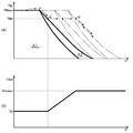
- FIG. 3 is an explanatory diagram showing an example of a change in the system voltage command value Vdct and a change in the operable region of the electric motor 4 associated therewith.
- FIG. 3B shows an example of a change in the system voltage command value Vdct when the rotational speed ⁇ increases.
- FIG. 3A shows an electric motor according to such a change in the system voltage command value Vdct.
- 4 shows the change in the operable region.
- a region indicated by a solid line is an operable region when the power supply voltage Vb is used as it is as the system voltage Vdc without being boosted
- a region indicated by a two-dot chain line is a case where the power supply voltage Vb is gradually boosted.
- the operable region that changes is shown in FIG.
- a plurality of black dots in FIG. 3A indicate changes in the target torque TM.
- the control device 2 executes maximum torque control and PWM control.
- the operating point of the electric motor 4 enters the area A2 where field weakening control and rectangular wave control need to be performed, and the control device 2 performs field weakening control and Perform rectangular wave control.
- the control device 2 does not perform step-up control, and the system voltage command value Vdct remains the same value as the power supply voltage Vb. Therefore, the torque that can be output by the electric motor 4 gradually decreases as the rotational speed ⁇ increases.
- the control device 2 executes the boost control.
- the system voltage command value Vdct gradually increases from the same value as the power supply voltage Vb to the value Vdcmax set as the upper limit of the system voltage command value Vdct as the rotational speed ⁇ increases from time u2 to u3.
- Vdcmax which is the upper limit value of system voltage command value Vdct, be set to the upper limit value of system voltage Vdc that can be boosted by converter 5.
- the system voltage command value Vdct is increased as the rotational speed ⁇ of the electric motor 4 increases, so that the torque that can be output by the electric motor 4 is maintained constant even while the rotational speed ⁇ is increased.
- the relationship between the rotational speed ⁇ of the electric motor 4 and the torque that can be output during the boost control varies depending on the relationship between the boost speed and the acceleration of the rotor of the electric motor 4.
- the control device 2 executes field weakening control and rectangular wave control even during such boost control.
- the system voltage command value Vdct reaches its upper limit value Vdcmax.
- the torque that can be output by the electric motor 4 gradually decreases as the rotational speed ⁇ increases.
- the control device 2 executes field-weakening control and rectangular wave control during this time.
- the field weakening control and the rectangular wave control are first performed before the boost control is performed. Start (time u1 to u2). Thereafter, when the rotational speed ⁇ and the target torque TM are further increased, the system voltage Vdc is increased while maintaining the field weakening control and the rectangular wave control. Therefore, the effect of reducing the switching loss by the rectangular wave control can be obtained in a wide operating range, and the efficiency of the electric motor drive device 1 can be increased. Further, after system voltage command value Vdct reaches Vdcmax, which is the upper limit value, rotational speed ⁇ of electric motor 4 can be further increased by increasing the field weakening current.
- control device 2 is configured to execute the rectangular wave control even during the boost control by the converter 5. Then, when the converter 5 changes the system voltage Vdc during execution of the rectangular wave control in this way, the switching control unit 30 sets the length of one round of the electrical angle based on the change rate K of the system voltage Vdc.
- the rectangular wave width adjustment control for setting the on / off timing of the switching elements E3 to E8 is executed so that the time integration values of the three-phase rectangular wave voltages within the control period T are substantially the same between the phases.
- the overall operation of the control device 2, the rectangular wave width adjustment control, and the voltage conversion control will be described in this order.
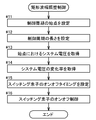
- FIG. 4 is a flowchart showing the flow of overall operation performed by the control device 2 during rectangular wave control.
- movement of the control apparatus 2 is demonstrated in order along the flowchart shown in FIG.
- the control device 2 acquires the system voltage command value Vdct (step # 01) and also acquires the system voltage Vdc (step # 02).
- the system voltage command value Vdct and the system voltage Vdc are compared to determine whether or not the system voltage Vdc needs to be changed (step # 03).
- step # 03 if there is a difference of a certain value or more between the system voltage command value Vdct and the system voltage Vdc, it is determined that the system voltage Vdc needs to be changed.
- the constant value is preferably determined according to an error included in the system voltage Vdc acquired by the system voltage sensor 42, a fluctuation range of the system voltage Vdc when the system voltage Vdc is not changed, or the like.
- the switching control unit 30 performs the rectangular wave width adjustment control described later (step # 04), and the voltage conversion control unit 31 determines the voltage described later. Conversion control is performed (step # 05).
- normal control is performed (step # 06).
- the normal control is to perform control such that the ratio of the high level period to the low level period in the rectangular wave voltage is a rectangular wave of 1: 1.
- FIG. 5 is a flowchart showing the flow of rectangular wave width adjustment control.
- FIG. 6 is an explanatory diagram for setting the on / off timing of the switching elements E3 to E8, which is executed by the rectangular wave width adjustment control.
- This example is an example in the case of increasing the system voltage Vdc, and specifically shows a case in which the system voltage Vdc increases at a constant rate of change K. Although description is omitted, when the system voltage Vdc is lowered, the on / off timings of the switching elements E3 to E8 can be set similarly to the procedure described below.
- FIG. 6A is a diagram showing a change over time in the system voltage Vdc.
- FIG. 6B is a diagram illustrating a temporal change in the U-phase voltage Vu supplied to the U-phase coil.
- FIG. 6C is a diagram illustrating a change over time of the V-phase voltage Vv supplied to the V-phase coil.
- FIG. 6D is a diagram showing a change over time of the W-phase voltage Vw supplied to the W-phase coil.
- the voltages of the U, V, and W phases are represented with reference to the half value (Vdc / 2) of the system voltage Vdc at each time point.
- the voltages Vu, Vv, and Vw of each phase have a voltage value of (+ Vdc / 2) in the high level period and have a voltage value of ( ⁇ Vdc / 2) in the low level period, centered on 0. It has become a wave.
- the voltage value of each phase increases with a slope of (K / 2), and in the low level period, the voltage value of each phase decreases with a slope of ( ⁇ K / 2).
- the rectangular wave width adjustment control is control performed by the switching control unit 30 when the converter 5 changes the system voltage Vdc during execution of the rectangular wave control.
- this rectangular wave width adjustment control based on the rate of change K of the system voltage Vdc, the time integration value of the three-phase rectangular wave voltage within the control period T set to the length of one round electrical angle is substantially the same between the phases.
- the on / off timings of the plurality of switching elements E3 to E8 are set so that In the following description, the point at which the voltage value of the rectangular wave voltage of each phase is switched between the high level and the low level by turning on and off the switching elements E3 to E8 is referred to as a high / low switching point.
- the switching control unit 30 matches the start point of the control cycle T with any of the high / low switching points when performing the rectangular wave width adjustment control. Then, based on the length of the control cycle T, the value of the system voltage Vdc at the start point of the control cycle T, and the rate of change K of the system voltage Vdc within the control cycle T, the time of the system voltage Vdc in each divided period
- the on / off timings of the switching elements E3 to E8 are set so that the integrated values are substantially the same.
- the division period is a period set by dividing the control cycle T with each of the high-low switching points of the three-phase rectangular wave voltage as division points.
- the switching control unit 30 sets the start point of the control cycle T (step # 11).
- the starting point of the control cycle T is set at time t0.
- Time t0 is a high-low switching point of the U-phase voltage Vu.
- the U-phase upper arm element E3 is changed from the ON state to the OFF state
- the U-phase lower arm element E4 is changed from the OFF state to the ON state.
- the U-phase voltage Vu is high.
- the length of the control cycle T is set (step # 12).
- the control cycle T is set to the length of one electrical angle, and in the example shown in FIG.
- the length of the control cycle T is (t6 ⁇ t0). That is, in this example, the end point of the control cycle T is time t6.
- This time t6 is a high-low switching point of the U-phase voltage Vu, and is the time when the U-phase voltage Vu is switched from the high level to the low level, similarly to the time t1.
- the system voltage Vdc at the start point of the control cycle T (in this example, time t0) is acquired (step # 13). In the example shown in FIG. 6, this value is V0.
- the rate of change K of the system voltage Vdc is acquired (step # 14).
- the voltage conversion control unit 31 is configured to calculate the rate of change K of the system voltage Vdc and input the rate of change K to the switching control unit 30.
- the switching control unit 30 determines the length of the control cycle T (t6 ⁇ t0), the value V0 of the system voltage Vdc at the start point t0 of the control cycle T, the rate of change K of the system voltage Vdc within the control cycle T, Based on the above, the on / off timings of the switching elements E3 to E8 are set so that the time integral values of the system voltage Vdc in each of the divided periods are substantially the same (step # 15).
- the W-phase upper arm element E7 is changed from the ON state to the OFF state, and the W-phase lower arm element E8 is changed from the OFF state to the ON state.
- the W-phase voltage Vw is changed from the high level to the low level. It is time to switch.
- the V-phase upper arm element E5 is changed from the OFF state to the ON state, and the V-phase lower arm element E6 is changed from the ON state to the OFF state.
- the V-phase voltage Vv is changed from the low level to the high level. It is time to switch.
- times t1 to t5 for determining the on / off timings (high / low switching points of the respective phases) of the switching elements E3 to E8 are set so that the time integration values of the system voltage Vdc in the respective divided periods are equal to each other.
- the area of the partition defined by the length of the divided period and the system voltage Vdc in the divided period is represented by s1 to s6. These areas s1 to s6 are equal to the time integration value of the system voltage Vdc in each divided period. Therefore, the switching control unit 30 sets times t1 to t5 so that the areas s1 to s6 are equal to each other.
- the times t1 to t5 may be calculated based on expressions other than the above expression (1).
- the correspondence between the length of the control cycle T, the value of the system voltage Vdc at the start point of the control cycle T, the rate of change K of the system voltage Vdc within the control cycle T, and the on / off timing of the switching elements E3 to E8 is shown. It is also preferable that the prepared map data is prepared in advance, and the on / off timings of the switching elements E3 to E8 are acquired and set with reference to the map data.
- the time integral value of the rectangular wave voltage of each phase can be made substantially the same between the phases. That is, as shown in FIG. 6B, regarding the U-phase voltage Vu, in all six divided periods, the areas of the sections determined by the length of the divided period and the U-phase voltage Vu in the divided period are equal to each other. Become.
- both the sum of the areas corresponding to the high level period (a1) and the sum of the areas corresponding to the low level period (a2) are three times the area of each of the above sections,
- the area a1 and the area a2 are equal to each other.
- the integral value of the U-phase voltage Vu in the high level period is equal to the area a1.
- the integral value of the U-phase voltage Vu in the low level period is equal to the area a2 multiplied by ( ⁇ 1). Since the area a1 and the area a2 are equal to each other as described above, the time integral value of the U-phase rectangular wave voltage Vu within the control period T is zero.
- the areas of the sections determined by the length of the divided period and the V-phase voltage Vv in the divided period are equal to each other. Become. That is, since the area of each section becomes equal, both the sum of the areas corresponding to the high level period (b1) and the sum of the areas corresponding to the low level period (b2) are three times the area of each of the above sections, The area b1 and the area b2 are equal to each other. In other words, the integrated value of the V-phase voltage Vv in the high level period is equal to the area b1.
- the integral value of the V-phase voltage Vv in the low level period is equal to the area b2 multiplied by ( ⁇ 1). Since the area b1 and the area b2 are equal to each other as described above, the time integration value of the V-phase rectangular wave voltage Vv within the control period T is zero.
- the areas of the sections determined by the length of the divided period and the W-phase voltage Vw in the divided period are equal to each other. Become. That is, since the area of each section becomes equal, both the sum of the areas corresponding to the high level period (c1) and the sum of the areas corresponding to the low level period (c2) are three times the area of each of the above sections, The area c1 and the area c2 are equal to each other. In other words, the integral value of the W-phase voltage Vw in the high level period is equal to the area c1.
- the integral value of the W-phase voltage Vw in the low level period is equal to the area c2 multiplied by ( ⁇ 1). Since the area c1 and the area c2 are equal to each other as described above, the time integral value of the W-phase rectangular wave voltage Vw within the control period T is zero. Thus, for each phase of U, V, and W within the control cycle T, the areas of the sections corresponding to the respective divided periods are equal to each other between the in-phase and between the different phases, whereby the time integral value of the rectangular wave voltage is obtained. Is equal between each phase.
- a plurality of switching elements are set so that the time integration values of the rectangular wave voltages of the U, V, and W phases within the control cycle T are substantially the same between the phases.
- the on / off timing of E3 to E8 can be set. Then, on / off control of the switching elements E3 to E8 within the control cycle T is performed according to the on / off timing of the switching elements E3 to E8 set as described above (step # 16).
- the on / off timings of the switching elements E3 to E8 are set so that the time integration values of the system voltage Vdc in each of the divided periods are substantially the same, so that The time integral value of the rectangular wave voltage of the phase can be made substantially the same between the phases.
- the system voltage Vdc can be changed while suppressing the vibration of the electric motor 4 even during the execution of the rectangular wave control, and the system voltage Vdc is not boosted up to the maximum system voltage Vdcmax as shown in FIG.
- the rectangular wave control can be performed from such a low rotation speed range. As a result, the use area of the rectangular wave control with little switching loss can be expanded to the low rotation speed area side, and the efficiency of the electric motor drive device 1 can be increased.
- the rectangular wave width adjustment control in the control cycle T set between time t0 and time t6. Only explained. Naturally, even when the system voltage Vdc does not change at a constant change rate K but changes in the control period K, the switching elements are set so that the time integration values of the system voltage Vdc in each divided period are substantially the same. By setting the on / off timing of E3 to E8, the time integration value of the three-phase rectangular wave voltage within the control cycle T can be made substantially the same between the phases.
- such rectangular wave width adjustment control repeatedly sets the control cycle T so that the end point of the control cycle T coincides with the start point of the next control cycle T in a situation where the system voltage Vdc continues to change,
- the rectangular wave width adjustment control can be repeatedly performed in each control period T.
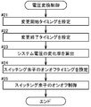
- FIG. 7 is a flowchart showing the flow of voltage conversion control.
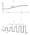
- FIG. 8 is an explanatory diagram of the control executed by the voltage conversion control.
- FIG. 8A is a diagram showing a time change of the system voltage Vdc.
- FIG. 8B shows the change over time of the U-phase voltage Vu supplied to the U-phase coil, with the half value (Vdc / 2) of the system voltage Vdc at each time point as a reference, as in FIG. 6B.
- FIG. Here, illustration of the V-phase voltage Vv and the W-phase voltage Vw is omitted.
- Voltage conversion control is control performed by the voltage conversion control unit 31 when the converter 5 changes the system voltage Vdc.
- a change start timing t10 for starting the change of the system voltage Vdc and a change end timing t20 for ending the change of the system voltage Vdc are set, and the rate of change K of the system voltage Vdc is calculated to start the change.
- On / off control of the switching elements E1 and E2 of the converter 5 is performed based on the timing t10, the change end timing t20, and the change rate K.
- the voltage conversion control unit 31 sets the change start timing t10 so as to coincide with any of the on / off timings of the switching elements E3 to E8 included in the inverter 6.
- the voltage conversion control unit 31 matches the change end timing t20 with the on / off timing that is different from the change start timing t10 by an integral multiple of the control cycle T among the on / off timings of the switching elements E3 to E8 included in the inverter 6.
- the operation of the voltage conversion control unit 31 will be described in order along the flowchart shown in FIG. 7 while referring to FIG. 8 as appropriate.
- the voltage conversion control unit 31 sets the change start timing t10 (step # 21).
- the change start timing t10 is set so as to coincide with the high / low switching point at which the U phase voltage Vu is switched from the high level to the low level among the high / low switching points.
- the start point of the control cycle T set first is set to coincide with the change start timing t10. Therefore, the rectangular wave width adjustment control can be performed from the initial time point when the change of the system voltage Vdc is started, and the generation of torque ripple can be more reliably suppressed.
- a change end timing t20 is set (step # 22).
- the change end timing t20 is the high-low switching of the U-phase voltage Vu after a time corresponding to an integral multiple of one round of electrical angle (three times of one round of electrical angle in this example) from the change start timing t10. It is set to match the point. Since the change end timing t20 is set in this way, the first control is performed when a plurality of (three in this example) control cycles T are continuously set between the change start timing t10 and the change end timing t20. The start point of the cycle T can be matched with the change start timing t10, and the end point of the last control cycle T can be matched with the change end timing t20. for that reason.
- the rectangular wave width adjustment control can be performed in all periods from the change start timing t10 to the change end timing t20, and the generation of torque ripple can be more reliably suppressed.
- a change rate K of the system voltage Vdc during the timing t20 is calculated (step # 23).
- K (V2-V1) / (t20-t10) (2)
- the voltage conversion control unit 31 then outputs the calculated change rate K of the system voltage Vdc to the switching control unit 30.
- the voltage conversion control unit 31 switches the switching element E1 included in the converter 5 to change the system voltage Vdc from V1 to V2 at a change rate K from the set change start timing t10 to the change end timing t20.
- the on / off timing of E2 is set (step # 24), and the on / off control of the switching elements E1 and E2 is performed (step # 25). Since the setting of the on / off timing of the switching elements E1 and E2 is known, detailed description thereof is omitted here.
- the rate of change K of the system voltage Vdc is calculated from the system voltage Vdc detected by the system voltage sensor 42.
- the system voltage sensor 42 smoothes the system voltage Vdc between the system voltage line 51 and the negative electrode line 52 of the inverter 6 as in the first embodiment. It is connected between the second smoothing capacitor C2 and the inverter 6.
- the control device 2 may process a power supply voltage detected by a power supply voltage sensor (not shown) that detects a voltage between terminals of the DC power supply 3 as the system voltage Vdc.
- a power supply voltage sensor not shown
- the control apparatus 2 which concerns on this embodiment is demonstrated centering around difference with said 1st embodiment. Note that points not particularly described are the same as those in the first embodiment.
- the DC power source 3 is constituted by a secondary battery as described above.
- the secondary battery has an internal resistance, and the terminal voltage drops or increases with respect to the electromotive force of the battery due to the internal resistance.
- the magnitude of this voltage drop or voltage rise is proportional to the value obtained by multiplying the value of the internal resistance by the value of the current flowing. Therefore, for example, when the electric motor 4 is powered or regenerated and a discharge current or a charging current is generated in the DC power supply 3, the system voltage Vdc changes due to a voltage drop or a voltage rise.
- the system voltage Vdc is also changed.
- the internal resistance increases in inverse proportion to the battery temperature. Therefore, for example, immediately after the motor drive device 1 is started, while the temperature of the DC power supply 3 is low, the internal resistance increases, and the change in the system voltage Vdc with respect to fluctuations in the discharge current and charging current of the DC power supply 3 increases. easy.
- rectangular wave width adjustment control is performed based on the rate of change K of the system voltage Vdc detected by the system voltage sensor 42.
- the overall operation of the control device 2 and the rectangular wave width adjustment control will be described in detail with respect to differences from the first embodiment.
- FIG. 10 is a flowchart showing the flow of the overall operation performed by the control device 2 according to this embodiment during the rectangular wave control.
- control device 2 detects and acquires the value of system voltage Vdc, and calculates system voltage change rate K (step # 31).
- the change rate K of the system voltage Vdc is calculated based on the value of the system voltage Vdc detected and acquired this time and the value of the system voltage Vdc detected and acquired in the past.
- the calculated change rate K is a predicted value of the change rate K during the next control cycle T.
- the rate of change K is, for example, based on the value V0 of the system voltage Vdc acquired this time, the value Vo1 of the system voltage Vdc acquired last time, and the interval ⁇ T1 from the previous acquisition to the current acquisition: ).
- the value of the system voltage Vdc acquired in the past and the acquisition interval are stored in a memory such as a RAM of the control device 2.
- K (V0 ⁇ Vo1) / ⁇ T1 (3)
- the execution timing of the acquisition of the system voltage Vdc and the calculation of the change rate K is synchronized with the start point of the control cycle T of the rectangular wave control, for example.
- the rate of change K may be calculated by various arithmetic expressions based on the value of the system voltage Vdc acquired at this time and a plurality of past points in time, and the acquisition intervals thereof. Further, the above execution timing may be set not in synchronization with the control cycle T but in synchronization with a predetermined cycle different from the control cycle T, for example. Further, the calculated change rate K or a value obtained by performing the filtering process on the detected system voltage Vdc may be used for other processing as the change rate K or the system voltage Vdc.
- the control device 2 determines whether or not a rectangular wave width adjustment control condition that is a condition for executing the rectangular wave width adjustment control is satisfied (step # 32). At this time, the control device 2 determines that the rectangular wave width adjustment control condition is satisfied when the system voltage Vdc is predicted to change. For example, the control device 2 determines that the rectangular wave width adjustment control condition is satisfied when the absolute value of the rate of change K calculated in step # 31 is equal to or greater than a predetermined threshold value.
- step # 32: Yes the switching control part 30 performs rectangular wave width adjustment control (step # 33).
- step # 34 the above-described normal control is performed (step # 34).
- the rectangular wave width adjustment control corresponding to step # 33 in the flowchart of FIG. 10 will be described.
- the rectangular wave width adjustment control according to this embodiment is the same as that of the first embodiment described with reference to FIGS. 5 and 6 except for the points described below.
- the change rate K acquired by the switching control unit 30 in step # 14 of FIG. 5 differs from that of the first embodiment in this embodiment in the system voltage Vdc acquired this time and the system acquired in the past.
- the predicted value of the rate of change K calculated in step # 31 of FIG.
- on / off timings of the switching elements E3 to E8 are set based on the predicted value of the change rate K in step # 15 of FIG.
- the system voltage in each divided period is the same as in the first embodiment.
- the on / off timing of the switching elements E3 to E8 can be set so that the time integration value of Vdc is substantially the same, and the time integration value of the three-phase rectangular wave voltage within the control cycle T is substantially the same between the phases. can do. Thereby, it can suppress that the balance of the voltage Vu, Vv, Vw supplied to the coil of each phase within the control period T can be suppressed, and generation
- the rectangular wave control can be performed while suppressing the vibration of the AC motor.
- the use area of the rectangular wave control with little switching loss can be expanded, and the efficiency of the electric motor drive device 1 can be increased.
- control cycle T is set to the length of one round electrical angle.
- the embodiment of the present invention is not limited to this. Therefore, the control cycle T may be set to a length that is an integral multiple of one round of electrical angle, such as twice or three times the round of electrical angle.
- the control cycle T may be set to a length that is an integral multiple of one round of electrical angle, such as twice or three times the round of electrical angle.
- the change start timing t10 for starting the change of the system voltage Vdc coincides with any of the on / off timings of the switching elements E3 to E8 included in the inverter 6, and the start point of the control cycle T is The case where it coincides with the change start timing t10 has been described as an example.
- the embodiment of the present invention is not limited to this. Accordingly, the start point of the control cycle T may be made to coincide with the on / off timing of the switching elements E3 to E8 different from the change start timing t10, or not to coincide with any of the on / off timings of the switching elements E3 to E8. This is one of the preferred embodiments. Further, it is also preferable that the change start timing t10 is not matched with any on / off timing.
- the change end timing t20 for ending the change of the system voltage Vdc is only three times the electrical angle round from the change start timing t10 among the on / off timings of the switching elements E3 to E8 included in the inverter.
- the case where the timing coincides with different on / off timings has been described as an example.
- the embodiment of the present invention is not limited to this. Therefore, the change end timing t20 is made to coincide with the on / off timing whose timing is different from the change start timing t10 by the same amount as the electric angle round, or an integer other than three times such as twice or four times the electric angle round from the change start timing t10.
- the timing is different from the on / off timing that is different by a factor of two.
- the change end timing t20 is matched with an on / off timing other than the on / off timing whose timing is different from the change start timing t10 by an integer multiple of an electrical angle, or is not matched with any of the on / off timings.
- the switching elements E3 to E8 are set so that the time integration values of the system voltage Vdc in each of the divided periods are substantially the same.
- the case where the on / off timing is set has been described as an example.
- the embodiment of the present invention is not limited to this. Therefore, the time integral value of the rectangular wave voltage of each phase within the control cycle T is substantially the same between the phases based on the rate of change K of the system voltage Vdc without considering the time integral value of the system voltage Vdc. It is one of preferred embodiments of the present invention to set the on / off timing of the switching elements E3 to E8 as described above.
- the high and low switching points of the U phase voltage Vu, the high and low switching points of the V phase voltage Vv, and the high and low switching points of the W phase voltage Vw are each independently determined as a rectangular wave voltage within the control cycle T.
- the time integral value can be set to be substantially the same between the phases.
- the start point of the control cycle T may be configured not to coincide with any of the high / low switching points.
- the case where the system voltage Vdc changes at a constant change rate K in the control cycle T has been described as an example.
- the embodiment of the present invention is not limited to this. If the time change of the change rate K in the control cycle T (time change of the system voltage Vdc) is known in advance, the rectangular shape in the control cycle T. Wave width adjustment control can be performed. In this case, the area calculation as in the above embodiment is not performed, and the time integration values of the system voltage Vdc and the rectangular wave voltages Vu, Vv, and Vw of each phase are calculated based on the time change of the change rate K.
- the on / off timing of the switching elements E3 to E8 can be set.
- the configuration in which the electric motor drive device 1 includes the boost converter 5 that boosts the power supply voltage Vb and generates the system voltage Vdc as the voltage conversion unit has been described as an example.
- the present invention is not limited to such an embodiment, and the present invention can be applied to the electric motor drive device 1 including various voltage conversion units that convert the power supply voltage Vb from the DC power supply 3 to generate a desired system voltage Vdc.
- the motor driving device 1 may include a step-up / down converter that performs both step-up and step-down of the power supply voltage Vb as a voltage conversion unit, or a step-down converter that performs step-down of the power supply voltage Vb. It is one of the preferred embodiments of the invention.
- the AC motor 4 is a synchronous motor (IPMSM) having an embedded magnet structure that operates by three-phase AC
- IPMSM synchronous motor
- the embodiment of the present invention is not limited to this.
- a synchronous motor (SPMSM) having a surface magnet structure can be used as the AC motor 4, or other than the synchronous motor, for example, induction An electric motor or the like can also be used.
- an alternating current supplied to such an alternating current motor a single-phase other than three phases, a two-phase, or a polyphase alternating current having four or more phases can be used.
- the switching control unit 30 is configured to acquire the rate of change K of the system voltage Vdc calculated by the voltage conversion control unit 31 in step # 14 of FIG.
- the switching control unit 30 changes based on the actual system voltage Vdc acquired in the past, as in the process described in step # 31 of FIG. 10 in the second embodiment. It is one of the preferred embodiments of the present invention that the predicted value of the rate K is calculated.
- the switching control unit 30 acquires the predicted value of the calculated change rate K as the change rate K in step # 14 of FIG. 5, and predicts the acquired change rate K in step # 15 of FIG. Based on the value, the ON / OFF timing of the switching element is set.
- the system voltage generation unit 32 has not been provided with the converter 5 and the control device 2 has not been provided with the voltage conversion control unit 31 as an example.
- the embodiment of the present invention is not limited to this. That is, in the second embodiment, similarly to the first embodiment shown in FIG. 1, the system voltage generation unit 32 includes the converter 5, and the control device 2 includes the voltage conversion control unit 31. May be. And when the voltage conversion control part 31 is not performing the voltage conversion control of pressure
- the present invention can be suitably used for a control device that controls an electric motor driving device for driving an AC electric motor.
- Motor drive device 2 Control device 3: DC power supply (system voltage generator) 4: Electric motor (AC motor) 5: Converter (system voltage generator, voltage converter) 6: Inverter (DC / AC converter) 30: Switching control unit 31: Voltage conversion control unit 32: System voltage generation unit E1 to E8: Switching element K: Change rate T: Control cycle Vb: Power supply voltage Vdc: System voltage Vdct: System voltage command value t10: Change start timing t20: Change end timing
Landscapes
- Engineering & Computer Science (AREA)
- Power Engineering (AREA)
- Control Of Ac Motors In General (AREA)
- Control Of Motors That Do Not Use Commutators (AREA)
- Inverter Devices (AREA)
Abstract
Description
従って、システム電圧が変化している状態においても、交流電動機の振動を抑えつつ矩形波制御を行うことができる。その結果、スイッチング損失の少ない矩形波制御の使用領域を拡大することができ、電動機駆動装置の効率を高めることができる。
また、システム電圧をコンバータなどにより能動的に昇圧又は降圧して、システム電圧を変更できるシステムにおいては、矩形波制御の実行中にも交流電動機の振動を抑えつつシステム電圧を変更することができ、システム電圧が最大システム電圧まで昇圧されていないような低回転速度域から矩形波制御を行うことができる。その結果、スイッチング損失の少ない矩形波制御の使用領域を低回転速度域側に拡大することができ、電動機駆動装置の効率を高めることができる。
なお、上記の3つのパラメータとオンオフタイミングとの対応関係を表したマップデータを予め準備しておき、当該マップデータを参照して複数のスイッチング素子のオンオフタイミングを取得して設定する構成としても好適である。
本発明の第一の実施形態について図面に基づいて説明する。図1に示すように、本実施形態においては、電動機駆動装置1が、三相交流により動作する交流電動機としての埋込磁石構造の同期電動機4(IPMSM、以下単に「電動機4」という。)を駆動する装置として構成されている場合を例として説明する。この電動機4は、必要に応じて発電機としても動作するように構成されており、例えば、電動車両やハイブリッド車両等の駆動力源として用いられる。電動機駆動装置1は、直流のシステム電圧を生成するシステム電圧生成部32と、当該システム電圧Vdcを互いに位相がずれた三相の交流電圧に変換して電動機4に供給するインバータ6とを有して構成されている。本実施形態では、システム電圧生成部32は、直流電源3と、当該直流電源3からの電源電圧Vbを変換して所望のシステム電圧Vdcを生成するコンバータ5とを備える。そして、本実施形態では、制御装置2は、ベクトル制御の手法を用いて電動機駆動装置1の制御を行い、インバータ6が備える複数のスイッチング素子E3~E8をオンオフ制御し、三相の矩形波状電圧を出力させる矩形波制御を実行可能に構成されている。この際、制御装置2は、矩形波制御の実行中にコンバータ5がシステム電圧Vdcを変更する場合には、システム電圧Vdcの変化率Kに基づいて、電気角一周の長さに設定された制御周期T内での各相の矩形波状電圧の時間積分値が各相間で略同一となるようにスイッチング素子E3~E8のオンオフタイミングを設定する矩形波幅調整制御を行う点に特徴を有している。以下、本実施形態に係る電動機駆動装置1及びその制御装置2について詳細に説明する。
まず、本実施形態に係る電動機駆動装置1の構成について図1に基づいて説明する。この電動機駆動装置1は、コンバータ5とインバータ6とを備えている。また、電動機駆動装置1は、直流電源3と、直流電源3からの直流電圧Vbを平滑化する第一平滑コンデンサC1と、コンバータ5による昇圧後のシステム電圧Vdcを平滑化する第二平滑コンデンサC2と、を備えている。直流電源3としては、例えば、ニッケル水素二次電池やリチウムイオン二次電池等の各種二次電池、キャパシタ、或いはこれらの組合せ等が用いられる。直流電源3の電圧である電源電圧Vbは、電源電圧センサ41により検出されて制御装置2へ出力される。
次に、本実施形態に係る制御装置2の機能について詳細に説明する。図1に示すように、制御装置2は、スイッチング制御部30と、電圧変換制御部31と、を備えている。これらの制御装置2の各機能部は、マイクロコンピュータ等の論理回路を中核部材として、入力されたデータに対して種々の処理を行うためのハードウェア又はソフトウェア(プログラム)或いはその両方により構成されている。上記のとおり、制御装置2には、目標トルクTM及び磁極位置θが入力される。そこで、スイッチング制御部30は、これらの目標トルクTM、磁極位置θ、及び磁極位置θから導出される電動機4の回転速度ωに応じて電動機4を駆動するためのスイッチング制御信号S3~S8を生成して出力し、インバータ6を駆動する。この際、制御装置2は、PWM制御及び最大トルク制御と、矩形波制御及び弱め界磁制御と、を切り替えてインバータ6を駆動する。また、制御装置2には、直流電源3の電源電圧Vb、コンバータ5により生成されたシステム電圧Vdc、及びシステム電圧指令値Vdctが入力される。そこで、電圧変換制御部31は、入力されたシステム電圧指令値Vdctと等しいシステム電圧Vdc生成するためのスイッチング制御信号S1、S2を生成して出力し、コンバータ5を駆動する。
次に、制御装置2の動作について説明する。上記のように、本実施形態では、制御装置2は、コンバータ5による昇圧制御中も矩形波制御を実行するように構成されている。そして、スイッチング制御部30は、このように矩形波制御の実行中にコンバータ5がシステム電圧Vdcを変更する場合には、システム電圧Vdcの変化率Kに基づいて、電気角一周の長さに設定された制御周期T内での三相の矩形波状電圧の時間積分値が各相間で略同一となるようにスイッチング素子E3~E8のオンオフタイミングを設定する矩形波幅調整制御を実行する。以下、制御装置2の全体動作、矩形波幅調整制御、電圧変換制御の順に説明する。
図4は、制御装置2が矩形波制御中に行う全体動作の流れを示すフローチャートである。以下、図4に示すフローチャートに沿って制御装置2の動作を順に説明する。まず、制御装置2は、システム電圧指令値Vdctを取得する(ステップ#01)とともに、システム電圧Vdcを取得する(ステップ#02)。そして、システム電圧指令値Vdctとシステム電圧Vdcとを比較し、システム電圧Vdcの変更が必要か否かの判定を行う(ステップ#03)。ここでは、システム電圧指令値Vdctとシステム電圧Vdcとの間に一定の値以上の差異があれば、システム電圧Vdcの変更が必要と判定する。ここで、一定の値は、システム電圧センサ42により取得されるシステム電圧Vdcに含まれる誤差や、システム電圧Vdcを変更しない状態におけるシステム電圧Vdcの変動幅等に応じて定めると好適である。そして、システム電圧Vdcの変更が必要な場合には(ステップ#03:Yes)、スイッチング制御部30が後述する矩形波幅調整制御を行うとともに(ステップ#04)、電圧変換制御部31が後述する電圧変換制御を行う(ステップ#05)。一方、システム電圧Vdcの変更が必要でない場合には(ステップ#03:No)、通常制御を行う(ステップ#06)。ここで通常制御とは、矩形波状電圧におけるハイレベル期間とローレベル期間との比が1:1の矩形波となるような制御を行うことである。
次に、図4のフローチャートにおけるステップ#04に対応する矩形波幅調整制御について、図5及び図6を用いて詳細に説明する。図5は、矩形波幅調整制御の流れを示すフローチャートである。図6は、矩形波幅調整制御により実行されるスイッチング素子E3~E8のオンオフタイミングの設定の説明図である。なお、本例は、システム電圧Vdcを上昇させる場合の例であり、具体的には、システム電圧Vdcが一定の変化率Kで上昇する場合を示している。説明は省略するが、システム電圧Vdcを下降させる場合も、以下に示す手順と同様にスイッチング素子E3~E8のオンオフタイミングを設定することができる。
{V0+K・(tn-t0)/2}・(tn-t0)・(6/n)
=(V0+K・T/2)・T・・・(1)
なお、当然ながら、上記の式(1)以外の式に基づいて時刻t1~t5を算出しても良い。また、制御周期Tの長さと、制御周期Tの始点におけるシステム電圧Vdcの値と、制御周期T内におけるシステム電圧Vdcの変化率Kと、スイッチング素子E3~E8のオンオフタイミングとの対応関係を表したマップデータを予め準備しておき、当該マップデータを参照してスイッチング素子E3~E8のオンオフタイミングを取得して設定する構成としても好適である。
次に、図4のフローチャートにおけるステップ#05に対応する電圧変換制御について、図7及び図8を用いて詳細に説明する。ここでは、システム電圧Vdcの現在値がV1であり、システム電圧指令値VdctとしてV2(>V1)が与えられた場合の制御を行う場合を例として説明する。なお、説明は省略するが、システム電圧Vdcを下降させる場合も、以下に示す手順と同様に電圧変換制御を行うことができる。図7は、電圧変換制御の流れを示すフローチャートである。図8は、電圧変換制御により実行される制御の説明図である。図8(a)は、システム電圧Vdcの時間変化を示す図である。図8(b)は、図6(b)と同様に各時点のシステム電圧Vdcの半値(Vdc/2)を基準として表した、U相のコイルに供給されるU相電圧Vuの時間変化を示す図である。なお、ここでは、V相電圧Vv及びW相電圧Vwについては図示を省略している。
させることができる。そのため。変更開始タイミングt10から変更終了タイミングt20までの全ての期間において矩形波幅調整制御を行うことができ、トルクリップルの発生をより確実に抑制することが可能となっている。
K=(V2-V1)/(t20-t10)・・・(2)
そして、電圧変換制御部31は、算出したシステム電圧Vdcの変化率Kを、スイッチング制御部30へ出力する。そして、電圧変換制御部31は、設定した変更開始タイミングt10から変更終了タイミングt20までの間、システム電圧VdcをV1からV2へ向かって変化率Kで変化させるべく、コンバータ5が備えるスイッチング素子E1、E2のオンオフタイミングを設定し(ステップ#24)、スイッチング素子E1、E2のオンオフ制御を行う(ステップ#25)。なお、スイッチング素子E1、E2のオンオフタイミングの設定は公知であるため、ここでは詳細な説明は省略する。
次に、本発明の第二の実施形態について説明する。上記の第一の実施形態では、システム電圧生成部32は、コンバータ5を備える場合を例に説明したが、本実施形態では、図9に示すように、システム電圧生成部32が、コンバータ5を備えず、直流電源3のみを備える場合を例に説明する。従って、本実施形態では、インバータ6は、コンバータ5を介さずに、直流電源3に接続されており、システム電圧Vdcは、直流電源3の出力電圧となる。そして、制御装置2は、第一の実施形態における電圧変換制御部31を備えず、スイッチング制御部30を備えている。スイッチング制御部30は、第一の実施形態とは異なり、電圧変換制御部31と協働すること無しに矩形波幅調整制御を実行する。また、システム電圧Vdcの変化率Kは、システム電圧センサ42により検出されたシステム電圧Vdcから算出される。ここで、システム電圧センサ42は、図9に示すように、第一の実施形態と同様に、インバータ6のシステム電圧線51と負極線52との間であって、システム電圧Vdcを平滑化する第二平滑コンデンサC2と、インバータ6との間に接続されている。なお、制御装置2は、直流電源3の端子間電圧を検出する図示しない電源電圧センサにより検出された電源電圧を、システム電圧Vdcとして処理するようにしてもよい。以下では、本実施形態に係る制御装置2について、上記第一の実施形態との相違点を中心として説明する。なお、特に説明しない点については、上記第一の実施形態と同様とする。
本実施形態では、システム電圧センサ42により検出したシステム電圧Vdcの変化率Kに基づき、矩形波幅調整制御を行う。以下、制御装置2の全体動作、矩形波幅調整制御について、第一の実施形態と異なる点について詳細に説明する。
図10は、本実施形態に係る制御装置2が矩形波制御中に行う全体動作の流れを示すフローチャートである。以下、図10に示すフローチャートに沿って制御装置2の動作を順に説明する。まず、制御装置2は、システム電圧Vdcの値を検出して取得し、システム電圧の変化率Kを算出する(ステップ♯31)。ここで、システム電圧Vdcの変化率Kは、今回検出して取得したシステム電圧Vdcの値と、過去に検出して取得したシステム電圧Vdcの値に基づき算出される。この算出された変化率Kは、次の制御周期Tの間における変化率Kの予測値となる。変化率Kは、例えば、今回取得したシステム電圧Vdcの値V0と、前回取得したシステム電圧Vdcの値Vo1と、前回取得してから今回取得するまでの間隔ΔT1とに基づき、下記の式(3)により算出される。ここで、過去に取得されたシステム電圧Vdcの値、及び取得間隔は、制御装置2のRAM等のメモリに記憶されている。
K=(V0-Vo1)/ΔT1・・・(3)
このシステム電圧Vdcの取得、及び変化率Kの算出の実行タイミングは、例えば、矩形波制御の制御周期Tの始点に同期する。なお、変化率Kの算出は、今回と、過去の複数時点とに取得したシステム電圧Vdcの値と、それらの取得間隔とに基づき、各種演算式により算出されるようにしてもよい。また、上記の実行タイミングは、制御周期Tに同期せずに、例えば制御周期Tとは別の所定周期に同期して設定されるようにしてもよい。また、算出した変化率K、あるいは検出したシステム電圧Vdcに対してフィルタ処理を行った値を、変化率K、あるいはシステム電圧Vdcとして、他の処理に用いるようにしてもよい。
次に、図10のフローチャートにおけるステップ#33に対応する矩形波幅調整制御について説明する。本実施形態に係る矩形波幅調整制御は、以下で説明する点を除き、図5、図6を用いて説明した第一の実施形態と同様である。具体的には、スイッチング制御部30が図5のステップ#14で取得する変化率Kが、第一の実施形態と異なり本実施形態では、今回取得したシステム電圧Vdcの値と過去に取得したシステム電圧Vdcの値とに基づき、図10のステップ♯31で算出された変化率Kの予測値とされる。そして、矩形波幅調整制御は、図5のステップ#15で、変化率Kの予測値に基づき、スイッチング素子E3~E8のオンオフタイミングを設定する。
(1)上記の実施形態では、制御周期Tが、電気角一周の長さに設定されている場合を例として説明した。しかし、本発明の実施形態はこれに限定されるものではない。従って、制御周期Tが、電気角一周の二倍や三倍の長さのような、電気角一周の整数倍の長さに設定される構成とすることも、本発明の好適な実施形態の一つである。
{Vn+K・Δtn/2}・Δtn・6=(V0+K・T/2)・T・・・(3)
ここで、Vnは、時刻tnにおけるシステム電圧Vdcであり、Δtnは、時刻tnと次の時刻との差である。すなわち、この構成では、制御周期Tの始点t0におけるシステム電圧Vdcの値V0、制御周期Tの長さ、制御周期Tにおけるシステム電圧Vdcの変化率Kに加え、時刻tnにおけるシステム電圧Vdcの値Vnに基づいて、時刻tnの次の時刻を算出する。なお、時刻tnが定まらないとVnを求めることができないので、この構成では、時刻t1、t2、t3、t4、t5を記載の順に算出することになる。
2:制御装置
3:直流電源(システム電圧生成部)
4:電動機(交流電動機)
5:コンバータ(システム電圧生成部、電圧変換部)
6:インバータ(直流交流変換部)
30:スイッチング制御部
31:電圧変換制御部
32:システム電圧生成部
E1~E8:スイッチング素子
K:変化率
T:制御周期
Vb:電源電圧
Vdc:システム電圧
Vdct:システム電圧指令値
t10:変更開始タイミング
t20:変更終了タイミング
Claims (5)
- 直流のシステム電圧を生成するシステム電圧生成部と、前記システム電圧を互いに位相がずれた複数相の交流電圧に変換して交流電動機に供給する直流交流変換部と、を備えた電動機駆動装置の制御を行う制御装置であって、
前記直流交流変換部が備える複数のスイッチング素子をオンオフ制御し、複数相の矩形波状電圧を出力させる矩形波制御を行うスイッチング制御部を備え、
前記スイッチング制御部は、前記矩形波制御の実行中に前記システム電圧が変化する場合には、前記システム電圧の変化率に基づいて、電気角一周の整数倍の長さに設定された制御周期内での各相の前記矩形波状電圧の時間積分値が各相間で略同一となるように前記複数のスイッチング素子のオンオフタイミングを設定する矩形波幅調整制御を行う電動機駆動装置の制御装置。 - 前記複数のスイッチング素子のオンオフにより各相の前記矩形波状電圧の電圧値がハイレベルとローレベルとの間で切り替わる点をハイロー切替点とするとともに、前記スイッチング制御部は、前記制御周期の始点を前記ハイロー切替点のいずれかと一致させ、
複数相の前記矩形波状電圧の前記ハイロー切替点のそれぞれを分割点として前記制御周期を分割して設定される期間を分割期間とし、
前記矩形波幅調整制御は、前記制御周期の長さと、前記制御周期の始点における前記システム電圧の値と、前記制御周期内における前記システム電圧の変化率と、に基づいて、前記分割期間のそれぞれにおける前記システム電圧の時間積分値が略同一となるように、前記複数のスイッチング素子のオンオフタイミングを設定する制御である請求項1に記載の電動機駆動装置の制御装置。 - 前記システム電圧生成部は、直流電源からの電源電圧を変換して所望の前記システム電圧を生成する電圧変換部を備え、
前記電圧変換部により生成する前記システム電圧の指令値であるシステム電圧指令値を取得するとともに、当該システム電圧指令値に基づいて、前記電圧変換部が備えるスイッチング素子のオンオフ制御を行う電圧変換制御部を更に備え、
前記電圧変換制御部は、前記電圧変換部に前記システム電圧を変更させる場合には、前記システム電圧の変更を開始する変更開始タイミングを前記直流交流変換部が備える前記複数のスイッチング素子のオンオフタイミングのいずれかと一致させ、
前記スイッチング制御部は、前記制御周期の始点を前記変更開始タイミングと一致させる請求項1又は2に記載の電動機駆動装置の制御装置。 - 前記電圧変換制御部は、前記システム電圧の変更を終了する変更終了タイミングを、前記直流交流変換部が備える前記複数のスイッチング素子のオンオフタイミングのうち、前記変更開始タイミングから電気角一周の整数倍だけタイミングが異なるオンオフタイミングと一致させる請求項3に記載の電動機駆動装置の制御装置。
- 前記システム電圧は、直流電源の出力電圧であり、
前記システム電圧の変化率は、前記制御周期の始点における前記システム電圧の値と、当該制御周期の始点より過去の前記システム電圧の値とに基づき算出される請求項1又は2に記載の電動機駆動装置の制御装置。
Priority Applications (4)
| Application Number | Priority Date | Filing Date | Title |
|---|---|---|---|
| CN201080010038.7A CN102342017B (zh) | 2009-06-22 | 2010-06-22 | 电机驱动装置的控制装置 |
| JP2011519906A JP5282985B2 (ja) | 2009-06-22 | 2010-06-22 | 電動機駆動装置の制御装置 |
| US13/254,279 US8624534B2 (en) | 2009-06-22 | 2010-06-22 | Control device for electric motor driving apparatus |
| DE112010000468T DE112010000468T5 (de) | 2009-06-22 | 2010-06-22 | Steuerungsvorrichtung für eineElektromotorantriebsvorrichtung |
Applications Claiming Priority (2)
| Application Number | Priority Date | Filing Date | Title |
|---|---|---|---|
| JP2009-147830 | 2009-06-22 | ||
| JP2009147830 | 2009-06-22 |
Publications (1)
| Publication Number | Publication Date |
|---|---|
| WO2010150786A1 true WO2010150786A1 (ja) | 2010-12-29 |
Family
ID=43386555
Family Applications (1)
| Application Number | Title | Priority Date | Filing Date |
|---|---|---|---|
| PCT/JP2010/060567 Ceased WO2010150786A1 (ja) | 2009-06-22 | 2010-06-22 | 電動機駆動装置の制御装置 |
Country Status (5)
| Country | Link |
|---|---|
| US (1) | US8624534B2 (ja) |
| JP (1) | JP5282985B2 (ja) |
| CN (1) | CN102342017B (ja) |
| DE (1) | DE112010000468T5 (ja) |
| WO (1) | WO2010150786A1 (ja) |
Cited By (4)
| Publication number | Priority date | Publication date | Assignee | Title |
|---|---|---|---|---|
| JP2012257358A (ja) * | 2011-06-08 | 2012-12-27 | Daikin Ind Ltd | インバータ制御方法及びモータ制御方法 |
| WO2020262269A1 (ja) * | 2019-06-26 | 2020-12-30 | 株式会社豊田自動織機 | 電動機の制御装置 |
| JP2021005996A (ja) * | 2019-06-26 | 2021-01-14 | 株式会社豊田自動織機 | 電動機の制御装置 |
| WO2025224990A1 (ja) * | 2024-04-26 | 2025-10-30 | 三菱電機モビリティ株式会社 | 回転電機装置の制御装置 |
Families Citing this family (15)
| Publication number | Priority date | Publication date | Assignee | Title |
|---|---|---|---|---|
| JP5633639B2 (ja) * | 2011-04-05 | 2014-12-03 | トヨタ自動車株式会社 | 電動機の制御装置およびそれを備える電動車両、ならびに電動機の制御方法 |
| WO2014076749A1 (ja) | 2012-11-13 | 2014-05-22 | トヨタ自動車株式会社 | 昇圧コンバータの制御装置 |
| DE112012007127T5 (de) * | 2012-11-13 | 2015-08-06 | Toyota Jidosha Kabushiki Kaisha | Aufwärtswandler-Steuerungsvorrichtung |
| CN105075097B (zh) * | 2013-04-23 | 2019-06-18 | 三菱电机株式会社 | 电力变换装置 |
| JP6364199B2 (ja) * | 2014-02-06 | 2018-07-25 | 日立オートモティブシステムズ株式会社 | 電力変換システム |
| JP2017045901A (ja) * | 2015-08-27 | 2017-03-02 | トヨタ自動車株式会社 | 還流ダイオードと車載用電源装置 |
| JP6591368B2 (ja) * | 2016-07-27 | 2019-10-16 | 株式会社東芝 | モータ制御用デバイス |
| US10576828B2 (en) * | 2017-01-12 | 2020-03-03 | Ford Global Technologies, Llc | Variable voltage converter modulation obtaining lower minimum boost ratio |
| WO2019044684A1 (ja) * | 2017-08-31 | 2019-03-07 | 日本電産トーソク株式会社 | モータの制御装置及び記憶媒体 |
| JP6889837B2 (ja) * | 2017-10-05 | 2021-06-18 | 株式会社ジェイテクト | モータ制御装置 |
| JP6989574B2 (ja) * | 2019-09-25 | 2022-01-05 | 本田技研工業株式会社 | 制御装置、車両システム及び制御方法 |
| CN114270688A (zh) * | 2019-08-30 | 2022-04-01 | 三菱电机株式会社 | 电力变换装置以及空气调节机 |
| JP7447838B2 (ja) * | 2021-02-05 | 2024-03-12 | 株式会社アイシン | 回転電機制御システム |
| DE102022132523A1 (de) * | 2022-12-07 | 2024-06-13 | HORIBA Europe GmbH, Zweigniederlassung Darmstadt | Antriebs- und Belastungssystem für eine rotierende elektrische Maschine, Prüfstand sowie elektrischer Belastungs- und Antriebsstrang |
| DE102024206146A1 (de) * | 2024-07-01 | 2026-01-08 | Robert Bosch Gesellschaft mit beschränkter Haftung | Elektrisches Bearbeitungsgerät mit einer Zwischenkreiselektronik |
Citations (2)
| Publication number | Priority date | Publication date | Assignee | Title |
|---|---|---|---|---|
| JP2001145384A (ja) * | 1999-11-12 | 2001-05-25 | Matsushita Electric Ind Co Ltd | 同期モータおよびその制御方法 |
| JP2004201487A (ja) * | 2002-11-28 | 2004-07-15 | Nsk Ltd | モータ及びその駆動制御装置 |
Family Cites Families (7)
| Publication number | Priority date | Publication date | Assignee | Title |
|---|---|---|---|---|
| JP4245546B2 (ja) * | 2004-11-04 | 2009-03-25 | トヨタ自動車株式会社 | 動力出力装置およびそれを備えた車両 |
| JP4604820B2 (ja) * | 2005-05-02 | 2011-01-05 | トヨタ自動車株式会社 | モータ駆動システムの制御装置 |
| JP2007159368A (ja) * | 2005-12-08 | 2007-06-21 | Toyota Motor Corp | モータ駆動システムの制御装置 |
| JP4802849B2 (ja) * | 2006-05-09 | 2011-10-26 | トヨタ自動車株式会社 | モータ駆動装置 |
| JP5109290B2 (ja) | 2006-05-30 | 2012-12-26 | トヨタ自動車株式会社 | 電動機駆動制御システムおよびその制御方法 |
| JP4720653B2 (ja) * | 2006-07-07 | 2011-07-13 | トヨタ自動車株式会社 | 電動機制御装置およびそれを備えた車両 |
| JP5172286B2 (ja) * | 2007-11-16 | 2013-03-27 | 日立オートモティブシステムズ株式会社 | モータ制御装置およびハイブリッド自動車用制御装置 |
-
2010
- 2010-06-22 US US13/254,279 patent/US8624534B2/en active Active
- 2010-06-22 WO PCT/JP2010/060567 patent/WO2010150786A1/ja not_active Ceased
- 2010-06-22 DE DE112010000468T patent/DE112010000468T5/de active Pending
- 2010-06-22 CN CN201080010038.7A patent/CN102342017B/zh active Active
- 2010-06-22 JP JP2011519906A patent/JP5282985B2/ja active Active
Patent Citations (2)
| Publication number | Priority date | Publication date | Assignee | Title |
|---|---|---|---|---|
| JP2001145384A (ja) * | 1999-11-12 | 2001-05-25 | Matsushita Electric Ind Co Ltd | 同期モータおよびその制御方法 |
| JP2004201487A (ja) * | 2002-11-28 | 2004-07-15 | Nsk Ltd | モータ及びその駆動制御装置 |
Cited By (7)
| Publication number | Priority date | Publication date | Assignee | Title |
|---|---|---|---|---|
| JP2012257358A (ja) * | 2011-06-08 | 2012-12-27 | Daikin Ind Ltd | インバータ制御方法及びモータ制御方法 |
| WO2020262269A1 (ja) * | 2019-06-26 | 2020-12-30 | 株式会社豊田自動織機 | 電動機の制御装置 |
| JP2021005996A (ja) * | 2019-06-26 | 2021-01-14 | 株式会社豊田自動織機 | 電動機の制御装置 |
| KR20220010751A (ko) * | 2019-06-26 | 2022-01-26 | 가부시키가이샤 도요다 지도숏키 | 전동기의 제어 장치 |
| JP7283356B2 (ja) | 2019-06-26 | 2023-05-30 | 株式会社豊田自動織機 | 電動機の制御装置 |
| KR102649191B1 (ko) | 2019-06-26 | 2024-03-18 | 가부시키가이샤 도요다 지도숏키 | 전동기의 제어 장치 |
| WO2025224990A1 (ja) * | 2024-04-26 | 2025-10-30 | 三菱電機モビリティ株式会社 | 回転電機装置の制御装置 |
Also Published As
| Publication number | Publication date |
|---|---|
| JPWO2010150786A1 (ja) | 2012-12-10 |
| US8624534B2 (en) | 2014-01-07 |
| DE112010000468T5 (de) | 2012-05-24 |
| CN102342017B (zh) | 2014-01-08 |
| CN102342017A (zh) | 2012-02-01 |
| JP5282985B2 (ja) | 2013-09-04 |
| US20130187583A1 (en) | 2013-07-25 |
Similar Documents
| Publication | Publication Date | Title |
|---|---|---|
| JP5282985B2 (ja) | 電動機駆動装置の制御装置 | |
| JP5246508B2 (ja) | 電動機駆動装置の制御装置 | |
| JP5133834B2 (ja) | 交流電動機の制御装置 | |
| JP4729526B2 (ja) | 電動機の駆動制御装置 | |
| JP4329855B2 (ja) | 交流モータの制御装置および交流モータの制御方法 | |
| JP5633639B2 (ja) | 電動機の制御装置およびそれを備える電動車両、ならびに電動機の制御方法 | |
| JP5574182B2 (ja) | 駆動制御装置 | |
| JP5893876B2 (ja) | モータ制御システム | |
| JP5369630B2 (ja) | 交流電動機の制御装置 | |
| CN103650333A (zh) | 车辆和车辆的控制方法 | |
| US9595890B2 (en) | Switching control apparatus of load drive system | |
| JP2012023885A (ja) | 交流電動機の制御装置および制御方法 | |
| JP5352330B2 (ja) | モータ駆動制御装置 | |
| JP2011109803A (ja) | 電動機の制御装置 | |
| JP2010200527A (ja) | モータ駆動システムの制御装置 | |
| JP5618948B2 (ja) | モータ制御システム | |
| JP5958400B2 (ja) | モータ駆動制御装置 | |
| JP5381218B2 (ja) | 電動機の制御装置 | |
| JP2010220306A (ja) | モータの制御装置 | |
| JP5392361B2 (ja) | 車両および車両の制御方法 | |
| JP5290048B2 (ja) | 車両のモータ制御システム | |
| JP5558057B2 (ja) | 電力変換装置 | |
| JP2011072103A (ja) | 交流電動機の制御装置 | |
| JP2010259227A (ja) | モータの制御装置 |
Legal Events
| Date | Code | Title | Description |
|---|---|---|---|
| WWE | Wipo information: entry into national phase |
Ref document number: 201080010038.7 Country of ref document: CN |
|
| 121 | Ep: the epo has been informed by wipo that ep was designated in this application |
Ref document number: 10792104 Country of ref document: EP Kind code of ref document: A1 |
|
| ENP | Entry into the national phase |
Ref document number: 2011519906 Country of ref document: JP Kind code of ref document: A |
|
| WWE | Wipo information: entry into national phase |
Ref document number: 112010000468 Country of ref document: DE Ref document number: 1120100004684 Country of ref document: DE |
|
| WWE | Wipo information: entry into national phase |
Ref document number: 13254279 Country of ref document: US |
|
| 122 | Ep: pct application non-entry in european phase |
Ref document number: 10792104 Country of ref document: EP Kind code of ref document: A1 |