WO2010143705A1 - Dispositif de source lumineuse de surface, appareil d'éclairage, dispositif de rétroéclairage - Google Patents
Dispositif de source lumineuse de surface, appareil d'éclairage, dispositif de rétroéclairage Download PDFInfo
- Publication number
- WO2010143705A1 WO2010143705A1 PCT/JP2010/059903 JP2010059903W WO2010143705A1 WO 2010143705 A1 WO2010143705 A1 WO 2010143705A1 JP 2010059903 W JP2010059903 W JP 2010059903W WO 2010143705 A1 WO2010143705 A1 WO 2010143705A1
- Authority
- WO
- WIPO (PCT)
- Prior art keywords
- light
- layer
- light source
- source device
- surface light
- Prior art date
Links
- 239000010410 layer Substances 0.000 claims description 659
- 239000000463 material Substances 0.000 claims description 127
- 239000000758 substrate Substances 0.000 claims description 110
- 238000009792 diffusion process Methods 0.000 claims description 104
- 239000002245 particle Substances 0.000 claims description 80
- 229920005989 resin Polymers 0.000 claims description 65
- 239000011347 resin Substances 0.000 claims description 65
- 239000012790 adhesive layer Substances 0.000 claims description 59
- 238000009826 distribution Methods 0.000 claims description 58
- 239000000203 mixture Substances 0.000 claims description 44
- 238000005401 electroluminescence Methods 0.000 claims description 17
- 238000006243 chemical reaction Methods 0.000 claims description 14
- 230000003098 cholesteric effect Effects 0.000 claims description 4
- 238000000605 extraction Methods 0.000 abstract description 65
- 230000000994 depressogenic effect Effects 0.000 abstract 2
- 239000006185 dispersion Substances 0.000 abstract 2
- 239000010408 film Substances 0.000 description 105
- 239000011521 glass Substances 0.000 description 55
- 230000000052 comparative effect Effects 0.000 description 48
- VZSRBBMJRBPUNF-UHFFFAOYSA-N 2-(2,3-dihydro-1H-inden-2-ylamino)-N-[3-oxo-3-(2,4,6,7-tetrahydrotriazolo[4,5-c]pyridin-5-yl)propyl]pyrimidine-5-carboxamide Chemical compound C1C(CC2=CC=CC=C12)NC1=NC=C(C=N1)C(=O)NCCC(N1CC2=C(CC1)NN=N2)=O VZSRBBMJRBPUNF-UHFFFAOYSA-N 0.000 description 33
- 239000011342 resin composition Substances 0.000 description 31
- 238000004519 manufacturing process Methods 0.000 description 27
- 230000008859 change Effects 0.000 description 26
- 238000000034 method Methods 0.000 description 24
- 239000000853 adhesive Substances 0.000 description 23
- 230000001070 adhesive effect Effects 0.000 description 23
- 239000003795 chemical substances by application Substances 0.000 description 21
- 230000000694 effects Effects 0.000 description 19
- 238000002834 transmittance Methods 0.000 description 18
- 239000004973 liquid crystal related substance Substances 0.000 description 17
- 229910052751 metal Inorganic materials 0.000 description 16
- 239000002184 metal Substances 0.000 description 16
- 238000007789 sealing Methods 0.000 description 15
- AFCARXCZXQIEQB-UHFFFAOYSA-N N-[3-oxo-3-(2,4,6,7-tetrahydrotriazolo[4,5-c]pyridin-5-yl)propyl]-2-[[3-(trifluoromethoxy)phenyl]methylamino]pyrimidine-5-carboxamide Chemical compound O=C(CCNC(=O)C=1C=NC(=NC=1)NCC1=CC(=CC=C1)OC(F)(F)F)N1CC2=C(CC1)NN=N2 AFCARXCZXQIEQB-UHFFFAOYSA-N 0.000 description 14
- 239000004986 Cholesteric liquid crystals (ChLC) Substances 0.000 description 13
- 239000011248 coating agent Substances 0.000 description 12
- 238000000576 coating method Methods 0.000 description 12
- 238000005259 measurement Methods 0.000 description 12
- 239000011159 matrix material Substances 0.000 description 10
- 238000010438 heat treatment Methods 0.000 description 9
- 230000005525 hole transport Effects 0.000 description 8
- 238000002347 injection Methods 0.000 description 8
- 239000007924 injection Substances 0.000 description 8
- 229920000098 polyolefin Polymers 0.000 description 8
- 238000001228 spectrum Methods 0.000 description 8
- 239000004925 Acrylic resin Substances 0.000 description 7
- 238000011156 evaluation Methods 0.000 description 7
- YLZOPXRUQYQQID-UHFFFAOYSA-N 3-(2,4,6,7-tetrahydrotriazolo[4,5-c]pyridin-5-yl)-1-[4-[2-[[3-(trifluoromethoxy)phenyl]methylamino]pyrimidin-5-yl]piperazin-1-yl]propan-1-one Chemical compound N1N=NC=2CN(CCC=21)CCC(=O)N1CCN(CC1)C=1C=NC(=NC=1)NCC1=CC(=CC=C1)OC(F)(F)F YLZOPXRUQYQQID-UHFFFAOYSA-N 0.000 description 6
- NIPNSKYNPDTRPC-UHFFFAOYSA-N N-[2-oxo-2-(2,4,6,7-tetrahydrotriazolo[4,5-c]pyridin-5-yl)ethyl]-2-[[3-(trifluoromethoxy)phenyl]methylamino]pyrimidine-5-carboxamide Chemical compound O=C(CNC(=O)C=1C=NC(=NC=1)NCC1=CC(=CC=C1)OC(F)(F)F)N1CC2=C(CC1)NN=N2 NIPNSKYNPDTRPC-UHFFFAOYSA-N 0.000 description 6
- 125000002723 alicyclic group Chemical group 0.000 description 6
- 238000006073 displacement reaction Methods 0.000 description 6
- 239000007789 gas Substances 0.000 description 6
- 238000002360 preparation method Methods 0.000 description 6
- 239000000126 substance Substances 0.000 description 6
- MKYBYDHXWVHEJW-UHFFFAOYSA-N N-[1-oxo-1-(2,4,6,7-tetrahydrotriazolo[4,5-c]pyridin-5-yl)propan-2-yl]-2-[[3-(trifluoromethoxy)phenyl]methylamino]pyrimidine-5-carboxamide Chemical compound O=C(C(C)NC(=O)C=1C=NC(=NC=1)NCC1=CC(=CC=C1)OC(F)(F)F)N1CC2=C(CC1)NN=N2 MKYBYDHXWVHEJW-UHFFFAOYSA-N 0.000 description 5
- 230000000295 complement effect Effects 0.000 description 5
- 150000001875 compounds Chemical class 0.000 description 5
- 230000001788 irregular Effects 0.000 description 5
- 230000004048 modification Effects 0.000 description 5
- 238000012986 modification Methods 0.000 description 5
- 239000012780 transparent material Substances 0.000 description 5
- 229920000178 Acrylic resin Polymers 0.000 description 4
- 239000004820 Pressure-sensitive adhesive Substances 0.000 description 4
- -1 aromatic diamine compound Chemical class 0.000 description 4
- 230000008901 benefit Effects 0.000 description 4
- 230000015572 biosynthetic process Effects 0.000 description 4
- 239000011247 coating layer Substances 0.000 description 4
- 239000000945 filler Substances 0.000 description 4
- 230000006870 function Effects 0.000 description 4
- 230000001678 irradiating effect Effects 0.000 description 4
- 150000002736 metal compounds Chemical class 0.000 description 4
- 238000002156 mixing Methods 0.000 description 4
- 229910052757 nitrogen Inorganic materials 0.000 description 4
- 230000003287 optical effect Effects 0.000 description 4
- 229920002050 silicone resin Polymers 0.000 description 4
- 238000004088 simulation Methods 0.000 description 4
- 239000002356 single layer Substances 0.000 description 4
- 230000003595 spectral effect Effects 0.000 description 4
- 238000012546 transfer Methods 0.000 description 4
- ZWEHNKRNPOVVGH-UHFFFAOYSA-N 2-Butanone Chemical compound CCC(C)=O ZWEHNKRNPOVVGH-UHFFFAOYSA-N 0.000 description 3
- 239000003522 acrylic cement Substances 0.000 description 3
- 239000000956 alloy Substances 0.000 description 3
- 229910045601 alloy Inorganic materials 0.000 description 3
- 229910052782 aluminium Inorganic materials 0.000 description 3
- XAGFODPZIPBFFR-UHFFFAOYSA-N aluminium Chemical compound [Al] XAGFODPZIPBFFR-UHFFFAOYSA-N 0.000 description 3
- 238000005452 bending Methods 0.000 description 3
- 230000005540 biological transmission Effects 0.000 description 3
- 239000003086 colorant Substances 0.000 description 3
- 230000007423 decrease Effects 0.000 description 3
- 238000000295 emission spectrum Methods 0.000 description 3
- UHESRSKEBRADOO-UHFFFAOYSA-N ethyl carbamate;prop-2-enoic acid Chemical compound OC(=O)C=C.CCOC(N)=O UHESRSKEBRADOO-UHFFFAOYSA-N 0.000 description 3
- 238000005286 illumination Methods 0.000 description 3
- PJXISJQVUVHSOJ-UHFFFAOYSA-N indium(iii) oxide Chemical compound [O-2].[O-2].[O-2].[In+3].[In+3] PJXISJQVUVHSOJ-UHFFFAOYSA-N 0.000 description 3
- 239000007788 liquid Substances 0.000 description 3
- PQXKHYXIUOZZFA-UHFFFAOYSA-M lithium fluoride Chemical compound [Li+].[F-] PQXKHYXIUOZZFA-UHFFFAOYSA-M 0.000 description 3
- 150000002739 metals Chemical class 0.000 description 3
- IBHBKWKFFTZAHE-UHFFFAOYSA-N n-[4-[4-(n-naphthalen-1-ylanilino)phenyl]phenyl]-n-phenylnaphthalen-1-amine Chemical group C1=CC=CC=C1N(C=1C2=CC=CC=C2C=CC=1)C1=CC=C(C=2C=CC(=CC=2)N(C=2C=CC=CC=2)C=2C3=CC=CC=C3C=CC=2)C=C1 IBHBKWKFFTZAHE-UHFFFAOYSA-N 0.000 description 3
- 230000008569 process Effects 0.000 description 3
- 239000000047 product Substances 0.000 description 3
- 230000009467 reduction Effects 0.000 description 3
- 239000005268 rod-like liquid crystal Substances 0.000 description 3
- 239000012798 spherical particle Substances 0.000 description 3
- 229920005992 thermoplastic resin Polymers 0.000 description 3
- HJIAMFHSAAEUKR-UHFFFAOYSA-N (2-hydroxyphenyl)-phenylmethanone Chemical compound OC1=CC=CC=C1C(=O)C1=CC=CC=C1 HJIAMFHSAAEUKR-UHFFFAOYSA-N 0.000 description 2
- NIXOWILDQLNWCW-UHFFFAOYSA-M Acrylate Chemical compound [O-]C(=O)C=C NIXOWILDQLNWCW-UHFFFAOYSA-M 0.000 description 2
- 239000004372 Polyvinyl alcohol Substances 0.000 description 2
- 238000010521 absorption reaction Methods 0.000 description 2
- 230000004888 barrier function Effects 0.000 description 2
- 239000000470 constituent Substances 0.000 description 2
- 230000007547 defect Effects 0.000 description 2
- 238000013461 design Methods 0.000 description 2
- 239000002019 doping agent Substances 0.000 description 2
- 239000000975 dye Substances 0.000 description 2
- 239000003822 epoxy resin Substances 0.000 description 2
- 238000001125 extrusion Methods 0.000 description 2
- 238000007756 gravure coating Methods 0.000 description 2
- 230000006872 improvement Effects 0.000 description 2
- 229910003437 indium oxide Inorganic materials 0.000 description 2
- 230000007246 mechanism Effects 0.000 description 2
- DCZNSJVFOQPSRV-UHFFFAOYSA-N n,n-diphenyl-4-[4-(n-phenylanilino)phenyl]aniline Chemical class C1=CC=CC=C1N(C=1C=CC(=CC=1)C=1C=CC(=CC=1)N(C=1C=CC=CC=1)C=1C=CC=CC=1)C1=CC=CC=C1 DCZNSJVFOQPSRV-UHFFFAOYSA-N 0.000 description 2
- 230000002093 peripheral effect Effects 0.000 description 2
- 229920000058 polyacrylate Polymers 0.000 description 2
- 229920000647 polyepoxide Polymers 0.000 description 2
- 229920000728 polyester Polymers 0.000 description 2
- 229920006267 polyester film Polymers 0.000 description 2
- 229920005672 polyolefin resin Polymers 0.000 description 2
- 229920002451 polyvinyl alcohol Polymers 0.000 description 2
- 238000003825 pressing Methods 0.000 description 2
- 229910052594 sapphire Inorganic materials 0.000 description 2
- 239000010980 sapphire Substances 0.000 description 2
- 238000000926 separation method Methods 0.000 description 2
- 229910052709 silver Inorganic materials 0.000 description 2
- 239000004332 silver Substances 0.000 description 2
- 238000003892 spreading Methods 0.000 description 2
- 230000007480 spreading Effects 0.000 description 2
- 238000003860 storage Methods 0.000 description 2
- 239000004094 surface-active agent Substances 0.000 description 2
- 239000010409 thin film Substances 0.000 description 2
- 229910052727 yttrium Inorganic materials 0.000 description 2
- IERDDDBDINUYCD-UHFFFAOYSA-N 1-[4-[4-(9h-carbazol-1-yl)phenyl]phenyl]-9h-carbazole Chemical group C12=CC=CC=C2NC2=C1C=CC=C2C(C=C1)=CC=C1C(C=C1)=CC=C1C1=C2NC3=CC=CC=C3C2=CC=C1 IERDDDBDINUYCD-UHFFFAOYSA-N 0.000 description 1
- UWCWUCKPEYNDNV-LBPRGKRZSA-N 2,6-dimethyl-n-[[(2s)-pyrrolidin-2-yl]methyl]aniline Chemical compound CC1=CC=CC(C)=C1NC[C@H]1NCCC1 UWCWUCKPEYNDNV-LBPRGKRZSA-N 0.000 description 1
- NSMJMUQZRGZMQC-UHFFFAOYSA-N 2-naphthalen-1-yl-1H-imidazo[4,5-f][1,10]phenanthroline Chemical compound C12=CC=CN=C2C2=NC=CC=C2C2=C1NC(C=1C3=CC=CC=C3C=CC=1)=N2 NSMJMUQZRGZMQC-UHFFFAOYSA-N 0.000 description 1
- 229920002284 Cellulose triacetate Polymers 0.000 description 1
- 241000070918 Cima Species 0.000 description 1
- 241000284156 Clerodendrum quadriloculare Species 0.000 description 1
- 229920000089 Cyclic olefin copolymer Polymers 0.000 description 1
- 150000000918 Europium Chemical class 0.000 description 1
- ISWSIDIOOBJBQZ-UHFFFAOYSA-N Phenol Chemical compound OC1=CC=CC=C1 ISWSIDIOOBJBQZ-UHFFFAOYSA-N 0.000 description 1
- 239000004695 Polyether sulfone Substances 0.000 description 1
- 239000004698 Polyethylene Substances 0.000 description 1
- 239000004642 Polyimide Substances 0.000 description 1
- 239000004743 Polypropylene Substances 0.000 description 1
- 239000004793 Polystyrene Substances 0.000 description 1
- 229910052581 Si3N4 Inorganic materials 0.000 description 1
- 229910004298 SiO 2 Inorganic materials 0.000 description 1
- VYPSYNLAJGMNEJ-UHFFFAOYSA-N Silicium dioxide Chemical compound O=[Si]=O VYPSYNLAJGMNEJ-UHFFFAOYSA-N 0.000 description 1
- BQCADISMDOOEFD-UHFFFAOYSA-N Silver Chemical compound [Ag] BQCADISMDOOEFD-UHFFFAOYSA-N 0.000 description 1
- 229910010413 TiO 2 Inorganic materials 0.000 description 1
- GWEVSGVZZGPLCZ-UHFFFAOYSA-N Titan oxide Chemical compound O=[Ti]=O GWEVSGVZZGPLCZ-UHFFFAOYSA-N 0.000 description 1
- NNLVGZFZQQXQNW-ADJNRHBOSA-N [(2r,3r,4s,5r,6s)-4,5-diacetyloxy-3-[(2s,3r,4s,5r,6r)-3,4,5-triacetyloxy-6-(acetyloxymethyl)oxan-2-yl]oxy-6-[(2r,3r,4s,5r,6s)-4,5,6-triacetyloxy-2-(acetyloxymethyl)oxan-3-yl]oxyoxan-2-yl]methyl acetate Chemical compound O([C@@H]1O[C@@H]([C@H]([C@H](OC(C)=O)[C@H]1OC(C)=O)O[C@H]1[C@@H]([C@@H](OC(C)=O)[C@H](OC(C)=O)[C@@H](COC(C)=O)O1)OC(C)=O)COC(=O)C)[C@@H]1[C@@H](COC(C)=O)O[C@@H](OC(C)=O)[C@H](OC(C)=O)[C@H]1OC(C)=O NNLVGZFZQQXQNW-ADJNRHBOSA-N 0.000 description 1
- 238000005299 abrasion Methods 0.000 description 1
- NIXOWILDQLNWCW-UHFFFAOYSA-N acrylic acid group Chemical group C(C=C)(=O)O NIXOWILDQLNWCW-UHFFFAOYSA-N 0.000 description 1
- 239000000654 additive Substances 0.000 description 1
- 238000004220 aggregation Methods 0.000 description 1
- 230000002776 aggregation Effects 0.000 description 1
- 230000032683 aging Effects 0.000 description 1
- APLQAVQJYBLXDR-UHFFFAOYSA-N aluminum quinoline Chemical compound [Al+3].N1=CC=CC2=CC=CC=C12.N1=CC=CC2=CC=CC=C12.N1=CC=CC2=CC=CC=C12 APLQAVQJYBLXDR-UHFFFAOYSA-N 0.000 description 1
- 150000001412 amines Chemical class 0.000 description 1
- 150000001454 anthracenes Chemical class 0.000 description 1
- 239000002216 antistatic agent Substances 0.000 description 1
- 239000007864 aqueous solution Substances 0.000 description 1
- 239000012298 atmosphere Substances 0.000 description 1
- QVGXLLKOCUKJST-UHFFFAOYSA-N atomic oxygen Chemical compound [O] QVGXLLKOCUKJST-UHFFFAOYSA-N 0.000 description 1
- 239000010406 cathode material Substances 0.000 description 1
- 238000003851 corona treatment Methods 0.000 description 1
- 230000007797 corrosion Effects 0.000 description 1
- 238000005260 corrosion Methods 0.000 description 1
- 238000005520 cutting process Methods 0.000 description 1
- 230000006866 deterioration Effects 0.000 description 1
- 238000007607 die coating method Methods 0.000 description 1
- KPUWHANPEXNPJT-UHFFFAOYSA-N disiloxane Chemical class [SiH3]O[SiH3] KPUWHANPEXNPJT-UHFFFAOYSA-N 0.000 description 1
- 238000010894 electron beam technology Methods 0.000 description 1
- 238000001704 evaporation Methods 0.000 description 1
- 230000008020 evaporation Effects 0.000 description 1
- 230000001747 exhibiting effect Effects 0.000 description 1
- 230000002349 favourable effect Effects 0.000 description 1
- 239000007850 fluorescent dye Substances 0.000 description 1
- 125000000524 functional group Chemical group 0.000 description 1
- 230000009477 glass transition Effects 0.000 description 1
- LNEPOXFFQSENCJ-UHFFFAOYSA-N haloperidol Chemical compound C1CC(O)(C=2C=CC(Cl)=CC=2)CCN1CCCC(=O)C1=CC=C(F)C=C1 LNEPOXFFQSENCJ-UHFFFAOYSA-N 0.000 description 1
- 239000012943 hotmelt Substances 0.000 description 1
- 239000003112 inhibitor Substances 0.000 description 1
- 239000003999 initiator Substances 0.000 description 1
- 229910052741 iridium Inorganic materials 0.000 description 1
- GKOZUEZYRPOHIO-UHFFFAOYSA-N iridium atom Chemical compound [Ir] GKOZUEZYRPOHIO-UHFFFAOYSA-N 0.000 description 1
- 239000012948 isocyanate Substances 0.000 description 1
- 150000002513 isocyanates Chemical class 0.000 description 1
- 239000002346 layers by function Substances 0.000 description 1
- 230000031700 light absorption Effects 0.000 description 1
- 229910044991 metal oxide Inorganic materials 0.000 description 1
- 150000004706 metal oxides Chemical class 0.000 description 1
- 239000000113 methacrylic resin Substances 0.000 description 1
- 150000004767 nitrides Chemical class 0.000 description 1
- 239000012299 nitrogen atmosphere Substances 0.000 description 1
- 239000011368 organic material Substances 0.000 description 1
- TWNQGVIAIRXVLR-UHFFFAOYSA-N oxo(oxoalumanyloxy)alumane Chemical compound O=[Al]O[Al]=O TWNQGVIAIRXVLR-UHFFFAOYSA-N 0.000 description 1
- 239000001301 oxygen Substances 0.000 description 1
- 229910052760 oxygen Inorganic materials 0.000 description 1
- RVTZCBVAJQQJTK-UHFFFAOYSA-N oxygen(2-);zirconium(4+) Chemical compound [O-2].[O-2].[Zr+4] RVTZCBVAJQQJTK-UHFFFAOYSA-N 0.000 description 1
- 239000012466 permeate Substances 0.000 description 1
- 125000002080 perylenyl group Chemical group C1(=CC=C2C=CC=C3C4=CC=CC5=CC=CC(C1=C23)=C45)* 0.000 description 1
- 239000004033 plastic Substances 0.000 description 1
- 229920003023 plastic Polymers 0.000 description 1
- 230000010287 polarization Effects 0.000 description 1
- 229920002492 poly(sulfone) Polymers 0.000 description 1
- 229920001230 polyarylate Polymers 0.000 description 1
- 239000004417 polycarbonate Substances 0.000 description 1
- 229920000515 polycarbonate Polymers 0.000 description 1
- 229920006393 polyether sulfone Polymers 0.000 description 1
- 229920000573 polyethylene Polymers 0.000 description 1
- 229920001721 polyimide Polymers 0.000 description 1
- 229920001155 polypropylene Polymers 0.000 description 1
- 229920005990 polystyrene resin Polymers 0.000 description 1
- 229920005749 polyurethane resin Polymers 0.000 description 1
- 238000012545 processing Methods 0.000 description 1
- 150000003219 pyrazolines Chemical class 0.000 description 1
- 238000005546 reactive sputtering Methods 0.000 description 1
- 238000002310 reflectometry Methods 0.000 description 1
- YYMBJDOZVAITBP-UHFFFAOYSA-N rubrene Chemical compound C1=CC=CC=C1C(C1=C(C=2C=CC=CC=2)C2=CC=CC=C2C(C=2C=CC=CC=2)=C11)=C(C=CC=C2)C2=C1C1=CC=CC=C1 YYMBJDOZVAITBP-UHFFFAOYSA-N 0.000 description 1
- HQVNEWCFYHHQES-UHFFFAOYSA-N silicon nitride Chemical compound N12[Si]34N5[Si]62N3[Si]51N64 HQVNEWCFYHHQES-UHFFFAOYSA-N 0.000 description 1
- 229910052814 silicon oxide Inorganic materials 0.000 description 1
- 238000005549 size reduction Methods 0.000 description 1
- 238000009751 slip forming Methods 0.000 description 1
- 239000007787 solid Substances 0.000 description 1
- 239000002904 solvent Substances 0.000 description 1
- 230000001629 suppression Effects 0.000 description 1
- 229920003002 synthetic resin Polymers 0.000 description 1
- 239000000057 synthetic resin Substances 0.000 description 1
- 150000003518 tetracenes Chemical class 0.000 description 1
- 229920002803 thermoplastic polyurethane Polymers 0.000 description 1
- 229920001187 thermosetting polymer Polymers 0.000 description 1
- 150000003573 thiols Chemical class 0.000 description 1
- OGIDPMRJRNCKJF-UHFFFAOYSA-N titanium oxide Inorganic materials [Ti]=O OGIDPMRJRNCKJF-UHFFFAOYSA-N 0.000 description 1
- 150000003852 triazoles Chemical class 0.000 description 1
- 238000007738 vacuum evaporation Methods 0.000 description 1
- 238000007740 vapor deposition Methods 0.000 description 1
- 239000011800 void material Substances 0.000 description 1
- 229910001928 zirconium oxide Inorganic materials 0.000 description 1
Images


Classifications
-
- H—ELECTRICITY
- H10—SEMICONDUCTOR DEVICES; ELECTRIC SOLID-STATE DEVICES NOT OTHERWISE PROVIDED FOR
- H10K—ORGANIC ELECTRIC SOLID-STATE DEVICES
- H10K50/00—Organic light-emitting devices
- H10K50/80—Constructional details
- H10K50/85—Arrangements for extracting light from the devices
- H10K50/854—Arrangements for extracting light from the devices comprising scattering means
-
- H—ELECTRICITY
- H05—ELECTRIC TECHNIQUES NOT OTHERWISE PROVIDED FOR
- H05B—ELECTRIC HEATING; ELECTRIC LIGHT SOURCES NOT OTHERWISE PROVIDED FOR; CIRCUIT ARRANGEMENTS FOR ELECTRIC LIGHT SOURCES, IN GENERAL
- H05B33/00—Electroluminescent light sources
- H05B33/12—Light sources with substantially two-dimensional radiating surfaces
- H05B33/14—Light sources with substantially two-dimensional radiating surfaces characterised by the chemical or physical composition or the arrangement of the electroluminescent material, or by the simultaneous addition of the electroluminescent material in or onto the light source
-
- G—PHYSICS
- G02—OPTICS
- G02B—OPTICAL ELEMENTS, SYSTEMS OR APPARATUS
- G02B5/00—Optical elements other than lenses
- G02B5/04—Prisms
- G02B5/045—Prism arrays
-
- G—PHYSICS
- G02—OPTICS
- G02B—OPTICAL ELEMENTS, SYSTEMS OR APPARATUS
- G02B6/00—Light guides; Structural details of arrangements comprising light guides and other optical elements, e.g. couplings
- G02B6/0001—Light guides; Structural details of arrangements comprising light guides and other optical elements, e.g. couplings specially adapted for lighting devices or systems
- G02B6/0011—Light guides; Structural details of arrangements comprising light guides and other optical elements, e.g. couplings specially adapted for lighting devices or systems the light guides being planar or of plate-like form
- G02B6/0033—Means for improving the coupling-out of light from the light guide
- G02B6/0035—Means for improving the coupling-out of light from the light guide provided on the surface of the light guide or in the bulk of it
- G02B6/0036—2-D arrangement of prisms, protrusions, indentations or roughened surfaces
-
- G—PHYSICS
- G02—OPTICS
- G02F—OPTICAL DEVICES OR ARRANGEMENTS FOR THE CONTROL OF LIGHT BY MODIFICATION OF THE OPTICAL PROPERTIES OF THE MEDIA OF THE ELEMENTS INVOLVED THEREIN; NON-LINEAR OPTICS; FREQUENCY-CHANGING OF LIGHT; OPTICAL LOGIC ELEMENTS; OPTICAL ANALOGUE/DIGITAL CONVERTERS
- G02F1/00—Devices or arrangements for the control of the intensity, colour, phase, polarisation or direction of light arriving from an independent light source, e.g. switching, gating or modulating; Non-linear optics
- G02F1/01—Devices or arrangements for the control of the intensity, colour, phase, polarisation or direction of light arriving from an independent light source, e.g. switching, gating or modulating; Non-linear optics for the control of the intensity, phase, polarisation or colour
- G02F1/13—Devices or arrangements for the control of the intensity, colour, phase, polarisation or direction of light arriving from an independent light source, e.g. switching, gating or modulating; Non-linear optics for the control of the intensity, phase, polarisation or colour based on liquid crystals, e.g. single liquid crystal display cells
- G02F1/133—Constructional arrangements; Operation of liquid crystal cells; Circuit arrangements
- G02F1/1333—Constructional arrangements; Manufacturing methods
- G02F1/1335—Structural association of cells with optical devices, e.g. polarisers or reflectors
- G02F1/1336—Illuminating devices
- G02F1/133602—Direct backlight
- G02F1/133603—Direct backlight with LEDs
-
- H—ELECTRICITY
- H10—SEMICONDUCTOR DEVICES; ELECTRIC SOLID-STATE DEVICES NOT OTHERWISE PROVIDED FOR
- H10K—ORGANIC ELECTRIC SOLID-STATE DEVICES
- H10K50/00—Organic light-emitting devices
- H10K50/80—Constructional details
- H10K50/84—Passivation; Containers; Encapsulations
-
- H—ELECTRICITY
- H10—SEMICONDUCTOR DEVICES; ELECTRIC SOLID-STATE DEVICES NOT OTHERWISE PROVIDED FOR
- H10K—ORGANIC ELECTRIC SOLID-STATE DEVICES
- H10K50/00—Organic light-emitting devices
- H10K50/80—Constructional details
- H10K50/85—Arrangements for extracting light from the devices
- H10K50/856—Arrangements for extracting light from the devices comprising reflective means
-
- H—ELECTRICITY
- H10—SEMICONDUCTOR DEVICES; ELECTRIC SOLID-STATE DEVICES NOT OTHERWISE PROVIDED FOR
- H10K—ORGANIC ELECTRIC SOLID-STATE DEVICES
- H10K50/00—Organic light-emitting devices
- H10K50/80—Constructional details
- H10K50/85—Arrangements for extracting light from the devices
- H10K50/858—Arrangements for extracting light from the devices comprising refractive means, e.g. lenses
-
- H—ELECTRICITY
- H10—SEMICONDUCTOR DEVICES; ELECTRIC SOLID-STATE DEVICES NOT OTHERWISE PROVIDED FOR
- H10K—ORGANIC ELECTRIC SOLID-STATE DEVICES
- H10K59/00—Integrated devices, or assemblies of multiple devices, comprising at least one organic light-emitting element covered by group H10K50/00
- H10K59/80—Constructional details
- H10K59/87—Passivation; Containers; Encapsulations
- H10K59/871—Self-supporting sealing arrangements
-
- H—ELECTRICITY
- H10—SEMICONDUCTOR DEVICES; ELECTRIC SOLID-STATE DEVICES NOT OTHERWISE PROVIDED FOR
- H10K—ORGANIC ELECTRIC SOLID-STATE DEVICES
- H10K59/00—Integrated devices, or assemblies of multiple devices, comprising at least one organic light-emitting element covered by group H10K50/00
- H10K59/80—Constructional details
- H10K59/875—Arrangements for extracting light from the devices
- H10K59/878—Arrangements for extracting light from the devices comprising reflective means
-
- H—ELECTRICITY
- H10—SEMICONDUCTOR DEVICES; ELECTRIC SOLID-STATE DEVICES NOT OTHERWISE PROVIDED FOR
- H10K—ORGANIC ELECTRIC SOLID-STATE DEVICES
- H10K59/00—Integrated devices, or assemblies of multiple devices, comprising at least one organic light-emitting element covered by group H10K50/00
- H10K59/80—Constructional details
- H10K59/875—Arrangements for extracting light from the devices
- H10K59/879—Arrangements for extracting light from the devices comprising refractive means, e.g. lenses
-
- G—PHYSICS
- G02—OPTICS
- G02F—OPTICAL DEVICES OR ARRANGEMENTS FOR THE CONTROL OF LIGHT BY MODIFICATION OF THE OPTICAL PROPERTIES OF THE MEDIA OF THE ELEMENTS INVOLVED THEREIN; NON-LINEAR OPTICS; FREQUENCY-CHANGING OF LIGHT; OPTICAL LOGIC ELEMENTS; OPTICAL ANALOGUE/DIGITAL CONVERTERS
- G02F1/00—Devices or arrangements for the control of the intensity, colour, phase, polarisation or direction of light arriving from an independent light source, e.g. switching, gating or modulating; Non-linear optics
- G02F1/01—Devices or arrangements for the control of the intensity, colour, phase, polarisation or direction of light arriving from an independent light source, e.g. switching, gating or modulating; Non-linear optics for the control of the intensity, phase, polarisation or colour
- G02F1/13—Devices or arrangements for the control of the intensity, colour, phase, polarisation or direction of light arriving from an independent light source, e.g. switching, gating or modulating; Non-linear optics for the control of the intensity, phase, polarisation or colour based on liquid crystals, e.g. single liquid crystal display cells
- G02F1/133—Constructional arrangements; Operation of liquid crystal cells; Circuit arrangements
- G02F1/1333—Constructional arrangements; Manufacturing methods
- G02F1/1335—Structural association of cells with optical devices, e.g. polarisers or reflectors
- G02F1/1336—Illuminating devices
- G02F1/133602—Direct backlight
- G02F1/133606—Direct backlight including a specially adapted diffusing, scattering or light controlling members
- G02F1/133607—Direct backlight including a specially adapted diffusing, scattering or light controlling members the light controlling member including light directing or refracting elements, e.g. prisms or lenses
-
- H—ELECTRICITY
- H10—SEMICONDUCTOR DEVICES; ELECTRIC SOLID-STATE DEVICES NOT OTHERWISE PROVIDED FOR
- H10K—ORGANIC ELECTRIC SOLID-STATE DEVICES
- H10K59/00—Integrated devices, or assemblies of multiple devices, comprising at least one organic light-emitting element covered by group H10K50/00
- H10K59/80—Constructional details
- H10K59/875—Arrangements for extracting light from the devices
- H10K59/877—Arrangements for extracting light from the devices comprising scattering means
Definitions
- the present invention relates to a surface light source device, and a lighting fixture and a backlight device including the surface light source device.
- the light emitter of the organic electroluminescence element (hereinafter sometimes referred to as “organic EL element”) can have a planar shape, and the color of the light is white or a color close thereto. Therefore, it can be used as a light source of a lighting fixture that illuminates a space such as a living environment or as a backlight of a display device.
- a white organic EL element As an example of an organic EL element used for illumination, a white organic EL element is produced. Many of such white elements are laminated layers or light-emitting layers that generate a luminescent color having a complementary color relationship, which are referred to as a laminated type or a tandem type. These light emitting layer laminates are mainly yellow / blue or green / blue / red laminates.
- organic EL elements are low in efficiency for use in the above lighting applications. Therefore, when the organic EL element is used as a surface light source, it is required to increase its light extraction efficiency. For example, although the light emitting layer itself of the organic EL element has high luminous efficiency, the light amount is reduced due to interference or the like in the layer before it emits light through the laminated structure constituting the element. Such light loss is required to be reduced as much as possible.
- Patent Document 1 As a method for improving the light extraction efficiency of the organic EL element, it is known to provide various structures on the light extraction substrate. For example, it has been proposed to provide a prism containing a fluorescent compound on the light exit surface of the light source device (Patent Document 1), and to provide a microlens array (Patent Document 2). With these structures, good light collection can be achieved and efficiency is improved. As a means for increasing the light extraction efficiency, for example, Patent Document 3 discloses that a light diffusion medium is provided on the light emission side of the organic EL element to increase the overall luminance.
- Such color unevenness also occurs when the structures described in Patent Documents 1 and 2 are adopted in the above-described laminated organic EL element for illumination.
- the color unevenness is observed when the light emitting surface is observed from the front and from an angle inclined from the front because the depth from the light emitting surface to the light emitting layer differs depending on the light emitting layer of each color. In this case, it is observed as a phenomenon in which the color is greatly different.
- Patent Documents 1 and 2 when the structure described in Patent Documents 1 and 2 is adopted for a laminated type organic EL element for illumination, and a light-emitting surface of a light source device is provided with a concavo-convex structure such as a prism, the top of the concavo-convex structure is likely to be lost. There is a problem that it is difficult to increase the mechanical strength.
- the present invention has been made in view of the above, and a first object of the present invention is a surface light source device having high light extraction efficiency, little change in color depending on the observation angle, and high mechanical strength, It is providing a lighting fixture and a backlight apparatus.
- a second object of the present invention is a surface light source device that is excellent in productivity, can contribute to downsizing of the device, and can suppress a change in color depending on an observation angle, and uses this surface light source device. It is providing the lighting fixture and the backlight apparatus using this surface light source device.
- the inventors of the present invention have made extensive studies to solve the above problems. And it discovered that the 1st objective could be achieved by making the light emission surface of a surface light source device into a specific structure, and providing a diffusion member in a surface light source device. Based on this finding, the inventors have completed the first invention.
- the present inventor has found that the second object can be achieved by providing a diffusion unit and a light distribution distribution conversion unit together. Based on this finding, the present invention has been completed.
- a surface light source device comprising: an organic electroluminescent element including a light emitting layer; and a light emitting surface structure layer provided in contact with at least one surface of the organic electroluminescent element,
- the light-emitting surface structure layer has an uneven structure on the surface of the device light-emitting surface side
- the concavo-convex structure has a plurality of concave portions including slopes, and a flat portion located around each concave portion
- the surface light source device includes a diffusing member that receives light emitted from the light emitting layer and diffuses or transmits or reflects the incident light.
- the diffusing member is a member provided as a layer constituting part or all of the light exit surface structure layer, and is a member that transmits incident light in a diffused manner.
- the diffusion member is an adhesive layer interposed between two layers of the light exit surface structure layer.
- the light-emitting surface structure layer includes: A substrate provided in contact with the organic electroluminescence element; A concavo-convex structure layer provided at a position closer to the device light exit surface than the substrate, the concavo-convex structure layer having the concavo-convex structure on a surface closer to the device light exit surface; An adhesive layer for adhering the substrate and the concavo-convex structure layer,
- the surface light source device includes the adhesive layer as the diffusion member.
- the surface light source device, wherein the diffusing member is made of a material containing particles that impart light diffusibility.
- the surface light source device wherein the diffusion member is a member provided at a position farther from the light-emitting surface structure layer than the organic electroluminescence element, and reflects incident light in a diffused manner. .
- the ratio of the area occupied by the flat part to the total area occupied by the flat part and the area occupied by the concave part when the concavo-convex structure is observed from a direction perpendicular to the light exit surface of the device is 10 to 75% of the surface light source device.
- the concave portion has a pyramid shape, a conical shape, a partial spherical shape, or a combination thereof.
- the plurality of recesses are arranged on the device light exit surface along two or more directions intersecting each other, Between the said recessed parts adjacent, the clearance gap is provided in any direction of the said 2 or more direction, The said surface light source device with which the said clearance gap comprises the said flat part.
- the concave portion has a pyramid shape, a cone shape, a partial spherical shape, or a combination thereof,
- the plurality of recesses are arranged on the device light exit surface along two or more directions intersecting each other, The surface light source device, wherein a gap is provided only in one of the two or more directions between the adjacent recesses, and the gap constitutes the flat portion.
- the concave portion has a groove shape, The plurality of recesses are arranged in parallel on the device light exit surface, The said surface light source device with which a clearance gap is provided between the said adjacent recessed parts, and the said clearance gap comprises the said flat part.
- a lighting fixture including the surface light source device according to any one of [1] to [10].
- a backlight device comprising the surface light source device according to any one of [1] to [10].
- the second invention provides the following inventions.
- An organic electroluminescent element including a first electrode layer, a light emitting layer, and a second electrode layer in this order, and disposed in contact with at least one surface of the organic electroluminescent element, and emits light to the outside.
- a light-emitting side member having a light-exiting surface, wherein the light-emitting-side member has a light distribution distribution of light emitted from the organic electroluminescence element, and a normal direction of the light-exiting surface from the light-exiting surface.
- a light distribution distribution converter that converts the chromaticity of the light emitted along the light source and the chromaticity of the light emitted from the light emitting surface along an oblique direction intersecting the normal direction
- a surface light source device comprising: a diffusion unit that diffuses light emitted from the organic electroluminescence element.
- the diffusing unit is a layer formed of a composition including particles that are disposed between the light distribution distribution converting unit and the organic electroluminescence element and impart light diffusibility.
- the said surface light source device which is a layer comprised by the composition in which the said spreading
- the surface light source device wherein the light distribution distribution conversion unit includes an uneven structure layer having an uneven structure formed on a surface thereof.
- the concavo-convex structure layer is composed of a composition containing particles that impart light diffusibility, and also serves as the diffusion portion.
- the surface light source device including the light source distribution conversion unit, and a concavo-convex structure layer provided on a surface of the base material and having a concavo-convex structure formed on a surface opposite to the base material. .
- the surface light source device wherein the base material and / or the concavo-convex structure layer is composed of a composition containing particles that impart light diffusibility, and also serves as the diffusion portion.
- the surface light source device wherein the light distribution distribution conversion unit includes a base film and a selective reflection layer provided on at least one surface of the base film.
- a lighting fixture comprising the surface light source device.
- the surface light source device of the first aspect of the present invention has high light extraction efficiency, little change in color depending on the observation angle, and high mechanical strength of the light exit surface of the device. It is useful as a backlight of a display device. Since the lighting apparatus and the backlight device of the first aspect of the present invention have the surface light source device of the first aspect of the present invention, the light extraction efficiency is high, the change in color depending on the observation angle is small, and the mechanical strength is high. It can be set as a lighting fixture and a backlight apparatus.
- the surface light source device is superior in productivity because defects such as bending do not occur in the product, can contribute to downsizing of the device, and can suppress a change in color due to an observation angle. effective. Moreover, since it is a surface light source device which has such an effect, it is useful as the light source of a lighting fixture, the backlight apparatus of a liquid crystal display device, etc.
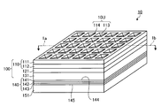
- FIG. 1 is a perspective view schematically showing a surface light source device according to Embodiment 1-1.
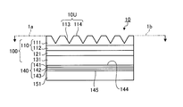
- FIG. 2 is a cross-sectional view showing a cross section of the surface light source device shown in FIG. 1 cut along a plane passing through line 1a-1b in FIG. 1 and perpendicular to the light output surface of the device.
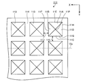
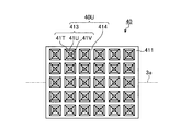
- FIG. 3 is an enlarged partial top view showing the structure of the device light exit surface 10U of the surface light source device 10 shown in FIG.
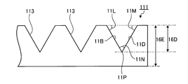
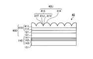
- FIG. 4 is a partial cross-sectional view showing a cross section of the concavo-convex structure layer 111 shown in FIG. 3 cut along a vertical plane passing through the line 10a of FIG.
- FIG. 5 is a partial cross-sectional view showing a modification of the recess shown in FIG. FIG.
- FIG. 6 is a partial cross-sectional view showing another modification of the recess shown in FIG.
- FIG. 7 is a top view schematically showing the surface light source device according to Embodiment 1-2.
- FIG. 8 is a cross-sectional view showing a cross section of the surface light source device shown in FIG. 7 cut along a plane passing through line 2a in FIG. 7 and perpendicular to the device light output surface.
- FIG. 9 is a perspective view schematically showing the surface light source device according to Embodiment 1-3.
- FIG. 10 is a top view schematically showing the surface light source device according to Embodiment 1-4.
- FIG. 11 is a cross-sectional view showing a cross section of the surface light source device shown in FIG. 10 cut along a plane that passes through the line 3a in FIG.
- FIG. 12 is a cross-sectional view showing a cross section of the surface light source device according to Embodiment 1-5 cut along a plane perpendicular to the device light exit surface.
- FIG. 13 is a top view schematically showing the surface light source device according to Embodiment 1-6.
- FIG. 14 is a cross-sectional view showing a cross section of the surface light source device shown in FIG. 13 cut along a plane passing through line 4a in FIG. 13 and perpendicular to the light output surface of the device.
- FIG. 15 is a top view schematically showing a concavo-convex structure layer according to a modification of Embodiment 1-6.
- FIG. 16 is a top view schematically showing the surface light source device according to Embodiment 1-7.
- FIG. 17 is a cross-sectional view showing a cross section of the surface light source device shown in FIG. 16 cut along a plane that passes through the line 11a-11b in FIG.
- FIG. 18 is a cross-sectional view schematically showing a cross section of the surface light source device according to Embodiment 1-8 taken along a plane perpendicular to the device light exit surface.
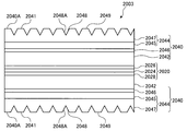
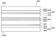
- FIG. 19 is a longitudinal sectional view for explaining a surface light source device according to Embodiment 2-1.
- FIG. 20 is a longitudinal sectional view for explaining a surface light source device according to Embodiment 2-2.
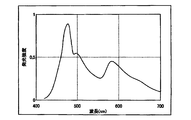
- FIG. 21 is a graph showing a spectrum of a light emitting layer used in the surface light source device.
- FIG. 22 is a graph showing the selective reflection characteristics of the selective reflection layer used in the surface light source device according to Embodiment 2-2.
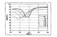
- FIG. 23 is a graph showing a light distribution of the surface light source device used for comparison with the surface light source device according to Embodiment 2-2.
- FIG. 24 is a graph showing a light distribution of the surface light source device used for comparison with the surface light source device according to Embodiment 2-2.
- FIG. 25 is a graph showing a light distribution of the surface light source device according to Embodiment 2-2.
- FIG. 26 is a longitudinal sectional view for explaining a surface light source device according to an embodiment of the second invention.
- FIG. 27 is a longitudinal sectional view for explaining a surface light source device according to an embodiment of the second invention.
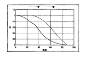
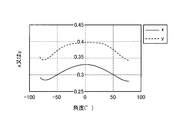
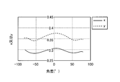
- FIG. 28 is a graph showing the relationship between the measurement angle of chromaticity and the chromaticity x and y values according to the measurement result of Comparative Example 1-1.
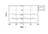
- FIG. 29 is a graph showing the relationship between the measurement angle of chromaticity and the chromaticity x and y values based on the measurement result of Example 1-1.
- FIG. 30 is a graph showing the relationship between the measurement angle of chromaticity and the chromaticity x and y values based on the measurement result of Example 1-2.
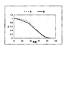
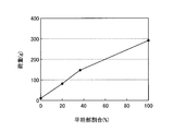
- FIG. 31 is a graph showing the relationship between the flat portion ratio and the load according to the measurement result of Reference Example 1-1.
- the surface light source device is provided in contact with at least one surface of an organic EL element including a light emitting layer and the organic EL element, and a light emitting surface structure that defines a concavo-convex structure on the surface on the device light emitting surface side.
- the device light exit surface is a light exit surface as a surface light source device, that is, a light exit surface when light exits from the surface light source device to the outside of the device.
- the device light exit surface is a surface parallel to the light emitting layer of the organic EL element, and is parallel to the main surface of the surface light source device.
- the surface on the concave portion described later can form an angle non-parallel to the light emitting layer.
- being parallel (or perpendicular) to the device exit surface viewed ignoring such recess is simply referred to as “parallel (or perpendicular) to the device exit surface”.
- the surface light source device will be described in a state where the device light-emitting surface is placed so as to be parallel to the horizontal direction and upward.
- the fact that each component is “parallel” or “perpendicular” may include an error within a range that does not impair the effects of the first aspect of the present invention. May include an error of ⁇ 5 °.
- Embodiment 1-1 is a first embodiment according to the first aspect of the present invention.
- FIG. 1 is a perspective view schematically showing a surface light source device according to Embodiment 1-1.
- the surface light source device 10 is a device having a rectangular plate-like structure having a device light exit surface 10U.
- FIG. 2 is a cross-sectional view showing a cross section of the surface light source device 10 shown in FIG. 1 taken along a plane passing through a line 1a-1b in FIG. 1 and perpendicular to the device light exit surface.
- the surface light source device 10 includes an organic EL element 140 and a light-emitting surface structure layer 100 provided in contact with the surface 144 of the organic EL element 140 on the device light-emitting surface 10U side.
- the surface light source device 10 further includes a sealing substrate 151 as an optional component on the surface 145 side of the organic EL element 140 opposite to the device light exit surface 10U.
- a sealing substrate 151 as an optional component on the surface 145 side of the organic EL element 140 opposite to the device light exit surface 10U.
- an arbitrary substance such as a filler or an adhesive may exist between the surface 145 and the sealing substrate 151, or a gap may exist.
- air or other gas may be present in the space, or the space may be evacuated.
- the organic EL element 140 includes a first electrode layer 141, a light emitting layer 142, and a second electrode layer 143.
- the first electrode layer 141 is a transparent electrode
- the second electrode layer 143 is a reflective electrode.
- the light exit surface structure layer 100 includes a multilayer body 110 including a concavo-convex structure layer 111 and a base film layer 112, a glass substrate 131 as a substrate provided in contact with the organic EL element 140, and the multilayer body 110 and the glass substrate. And an adhesive layer 121 for adhering 131.
- a material containing a diffusing agent particles that impart light diffusibility
- the diffusing member is configured to diffuse and transmit or reflect the incident light.
- the organic EL element 140 and the glass substrate 131 are in direct contact with each other, but other layers such as a diffusion layer may be interposed therebetween.
- the uneven structure layer 111 is located on the upper surface of the surface light source device 10 (that is, the outermost layer on the device light-emitting surface side of the surface light source device 10). Therefore, the concavo-convex structure layer 111 is provided at a position closer to the device light exit surface 10U than the glass substrate 131. Further, the concavo-convex structure layer 111 has a concavo-convex structure including a plurality of concave portions 113 and flat portions 114 located around the concave portions 113 on the surface near the device light exit surface 10U.
- the device light exit surface 10U is a plane parallel to other layers in the device such as the flat portion 114 and the glass substrate 131 when viewed macroscopically ignoring the recess 113, but is microscopically defined by the recess 113. It is an uneven surface including an inclined surface.
- the drawings are schematic illustrations, only a small number of recesses are shown on the device light-emitting surface. However, in an actual device, a single device light-emitting surface is shown here. A much larger number of recesses can be provided.
- the organic EL element 140 in the first aspect of the present invention, is provided between two or more electrode layers and these electrode layers, and emits light when a voltage is applied from the electrodes. A light emitting layer.
- a layer such as an electrode or a light emitting layer constituting the element is formed on a substrate, a sealing member that covers those layers is further provided, and the layer such as the light emitting layer is sealed with the substrate and the sealing member.
- the element that emits light from the substrate side here is called a bottom emission type
- the element that emits light from the sealing member side is called a top emission type.
- the surface light source device of the first aspect of the present invention may be any of these, and in the case of the bottom emission type, a combination of a substrate for forming a layer and an optional layer as necessary is a light emitting surface.
- the top emission type which constitutes the structural layer, a combination including a structure on the device light emitting surface side such as a sealing member and an optional layer as necessary constitutes the light emitting surface structural layer.
- the light emitting layer constituting the organic EL element is not particularly limited and a known one can be appropriately selected.
- the light-emitting material in the light-emitting layer is not limited to one type, and the light-emitting layer is not limited to one layer, and may be a single layer or a combination of a plurality of layers in order to suit the use as a light source. Thereby, light of white or a color close thereto can be emitted.
- the organic EL device may further include other layers such as a hole injection layer, a hole transport layer, an electron transport layer, an electron injection layer, and a gas barrier layer in addition to the light emitting layer between the electrodes.
- the organic EL element can further include arbitrary components such as a wiring for energizing the electrode and a peripheral structure for sealing the light emitting layer.
- the electrode of the organic EL element is not particularly limited, and a known one can be appropriately selected.
- an organic EL element that emits light to the light-emitting surface structure layer side by using the electrode on the light-emitting surface structure layer side as a transparent electrode and the electrode on the opposite side as a reflective electrode It can be.
- both of the electrodes are transparent electrodes, and further have a reflecting member or a scattering member (for example, a white scattering member disposed via an air layer) on the side opposite to the light emitting surface structure layer, thereby providing a light emitting surface structure layer. Light emission to the side can also be achieved.
- ITO etc. can be mentioned as a material of a transparent electrode.
- the material for the hole injection layer include a starburst aromatic diamine compound.
- the material for the hole transport layer include triphenyldiamine derivatives.
- the host material for the yellow light-emitting layer include triphenyldiamine derivatives, and examples of the dopant material for the yellow light-emitting layer include tetracene derivatives.
- the material for the green light emitting layer include pyrazoline derivatives.
- Examples of the host material for the blue light emitting layer include anthracene derivatives, and examples of the dopant material for the blue light emitting layer include perylene derivatives.
- Examples of the material for the red light emitting layer include europium complexes.
- Examples of the material for the electron transport layer include an aluminum quinoline complex (Alq).
- Examples of the cathode material include lithium fluoride and aluminum, which are sequentially stacked by vacuum film formation.
- a light emitting layer that generates a light emission color having a complementary color relationship which is called a laminated type or a tandem type, can be obtained by appropriately combining the above or other light emitting layers.
- the combination of complementary colors can be yellow / blue, green / blue / red, or the like.
- the light exit surface structure layer 100 may be composed of a plurality of layers, but may be composed of a single layer. From the viewpoint of easily obtaining a light-emitting surface structure layer having desired characteristics, it is preferably composed of a plurality of layers.
- corrugated structure layer and the base film layer can be included. Thereby, a light-emitting surface structure layer with high performance can be easily obtained.
- the resin composition constituting the concavo-convex structure layer and the base film can be a composition containing a transparent resin. That the transparent resin is “transparent” means that it has a light transmittance suitable for use in an optical member.
- each layer constituting the light exit surface structure layer can have a light transmittance suitable for use in an optical member, and the light exit surface structure layer as a whole has a total light beam of 80% or more. It can have transmittance.
- the material of the transparent resin contained in the resin composition is not particularly limited, and various resins that can form a transparent layer can be used. Examples thereof include a thermoplastic resin, a thermosetting resin, an ultraviolet curable resin, and an electron beam curable resin.
- thermoplastic resins are preferable because they can be easily deformed by heat, and ultraviolet curable resins have high curability and high efficiency, so that an uneven structure layer can be formed efficiently.
- thermoplastic resin include polyester-based, polyacrylate-based, and cycloolefin polymer-based resins.
- ultraviolet curable resin include epoxy resins, acrylic resins, urethane resins, ene / thiol resins, and isocyanate resins. As these resins, those having a plurality of polymerizable functional groups can be preferably used.
- a material having a high hardness at the time of curing is preferable from the viewpoint of easily forming the concavo-convex structure on the light emitting surface of the device and easily obtaining scratch resistance of the concavo-convex structure.
- a material having a pencil hardness of HB or higher is preferable, and a material of H or higher is more preferable. The material which becomes 2H or more is more preferable.
- the material of the base film layer has a certain degree of flexibility in order to facilitate the handling of the multilayer body when forming the concavo-convex structure layer and / or after forming the multilayer body.
- a multilayer body that is easy to handle and excellent in durability can be obtained, and as a result, a high-performance surface light source device can be easily manufactured.
- Such a combination of materials can be obtained by appropriately selecting the transparent resin exemplified above as the resin constituting each material.
- an ultraviolet curable resin such as acrylate is used as the transparent resin constituting the material of the concavo-convex structure layer
- the alicyclic olefin polymer film (described later) is used as the transparent resin constituting the material of the base film.
- Zeonor film, etc.) and polyester film can be used, whereby a preferable combination of materials can be obtained.
- the refractive index of the uneven structure layer and the base film may be as close as possible.
- the difference in refractive index is preferably within 0.1, more preferably within 0.05.
- a resin composition that is a material of a layer that is a constituent element of a light exit surface structure layer such as an uneven structure layer or a base film layer imparts light diffusibility such as particles described later when the layer constitutes a diffusion member. Elements can be included. Furthermore, the resin composition can contain arbitrary components as needed. Examples of the optional component include additives such as phenol-based and amine-based deterioration inhibitors; surfactant-based, siloxane-based antistatic agents; triazole-based, 2-hydroxybenzophenone-based light-resistant agents; be able to.
- the thickness of the concavo-convex structure layer is not particularly limited, but is preferably 1 to 70 ⁇ m.
- the thickness of the concavo-convex structure layer is the distance between the substrate-side surface where the concavo-convex structure is not formed and the flat portion of the concavo-convex structure.
- the thickness of the base film layer is preferably 20 to 300 ⁇ m.
- the light exit surface structure layer can further include a substrate such as a glass substrate 131 in the light exit surface structure layer 100, thereby giving the surface light source device rigidity to suppress deflection. it can. Further, by providing a substrate that is excellent in the performance of sealing the organic EL element as a substrate and that can easily form the layers constituting the organic EL element in the manufacturing process in order, a surface light source The durability of the device can be improved and the manufacture can be facilitated.
- the material constituting the substrate resin can be cited in addition to glass.
- the refractive index of the substrate is not particularly limited, but can be 1.4 to 2.
- the thickness of the substrate is not particularly limited, but is preferably 0.1 to 5 mm.
- the light exit surface structure layer may further include an adhesive layer interposed between two layers in the light exit surface structure layer, such as between the multilayer body and the substrate.
- the adhesive that is the material of the adhesive layer is not only a narrowly defined adhesive (a so-called hot melt type adhesive having a shear storage modulus of 1 to 500 MPa at 23 ° C. and does not exhibit tackiness at room temperature), A pressure-sensitive adhesive having a shear storage modulus at 1 ° C. of less than 1 MPa is also included.
- a material having a refractive index close to that of the substrate or the transparent resin layer and transparent can be used as appropriate. More specifically, an acrylic adhesive or a pressure-sensitive adhesive can be used.
- the thickness of the adhesive layer is preferably 5 to 100 ⁇ m.
- the surface light source device of the first aspect of the present invention is a layer constituting a part or all of the light exit surface structure layer, as a member provided at a position farther from the light exit surface structure layer than the organic EL element, or Both of them further include a diffusing member that diffuses and transmits or reflects incident light. That is, in the first aspect of the present invention, a part or all of the light exit surface structure layer may have a function as a diffusing member. You may have.
- the diffusing member is a part of the light-emitting surface structure layer.
- the member provided as a layer which comprises all Comprising: It can be set as the member which permeate
- the material for the layer that diffuses light examples include a material containing particles and a material that is an alloy resin that diffuses light by mixing two or more kinds of resins. From the viewpoint that light diffusibility can be easily adjusted, a material containing particles, particularly a resin composition containing particles, is particularly preferable. In this case, since the particles are particles that impart light diffusibility, the composition containing the particles has light diffusibility.
- the particles contained in the diffusing member may be transparent or opaque.
- metals, metal compounds, resins, and the like can be used as the material for the particles.
- the metal compound include metal oxides and nitrides.
- Specific examples of metals and metal compounds include metals having high reflectivity such as silver and aluminum, and metal compounds such as silicon oxide, aluminum oxide, zirconium oxide, silicon nitride, tin-doped indium oxide, and titanium oxide.
- examples of the resin include methacrylic resin, polyurethane resin, and silicone resin.
- the shape of the particles can be a spherical shape, a cylindrical shape, a cubic shape, a rectangular parallelepiped shape, a pyramid shape, a conical shape, a star shape, or the like.
- the content ratio of the particles is preferably 1 to 80%, more preferably 5 to 50% in terms of the volume ratio in the total amount of the material constituting the diffusing member.
- the particle size of the particles is preferably 0.1 ⁇ m or more and 10 ⁇ m or less, more preferably 5 ⁇ m or less.
- the particle diameter is a 50% particle diameter in an integrated distribution obtained by integrating the volume-based particle amount with the particle diameter as the horizontal axis. The larger the particle size, the larger the content ratio of particles necessary for obtaining the desired effect, and the smaller the particle size, the smaller the content.
- the particle size is smaller, desired effects such as a reduction in change in color depending on the observation angle and an improvement in light extraction efficiency can be obtained with fewer particles.
- the particle shape is other than spherical, the diameter of the sphere having the same volume is used as the particle size.
- the difference between the refractive index of the particles and the refractive index of the transparent resin is preferably 0.05 to 0.5. More preferably, it is 07 to 0.5.
- either the particle or the refractive index of the transparent resin may be larger. If the refractive index of the particles and the transparent resin is too close, the diffusion effect cannot be obtained and the color unevenness is not suppressed. Conversely, if the difference is too large, the diffusion increases and the color unevenness is suppressed, but the light extraction effect is reduced. It will be.
- a layer constituting part or all of the light-emitting surface structure layer is used as a diffusing member, which of the layers constituting the light-emitting surface structure layer is not particularly limited and is selected from various viewpoints. can do.
- a layer containing a transparent resin is preferably used as the diffusion member.
- the concavo-convex structure layer is preferably a material having a high hardness as described above.
- a layer other than the concavo-convex structure layer and capable of imparting a property of being easily plastically deformed for example, a base film or an adhesive layer as the diffusion member.
- the adhesive layer is preferably a diffusion member.
- the adhesive layer is also preferable to use a layer other than the adhesive layer and the adhesive layer as the diffusion member. For example, by using an adhesive layer and a base film as a diffusion member and reducing the proportion of particles added to the base film, management in the manufacturing process of the base film is facilitated (for example, how often clogging occurs). Can be reduced).
- layers other than the uneven structure layer, the base film layer, the adhesive layer, and the glass substrate can be additionally provided in the light emitting surface structure layer, and the additional layer can be used as a diffusion member.
- the additional layer can be used as a diffusion member.
- the concavo-convex structure layer and the base film layer between the adhesive layer and the glass substrate, the surface on the light emitting layer side of the glass substrate, etc. (for example, between the electrode layer constituting the light emitting layer and the glass substrate) can be formed.
- both of the additional layer and the concavo-convex structure layer, the base film layer, the adhesive layer, and one or more layers of the glass substrate may be used as the diffusing member.
- the degree of diffusion is not particularly limited, but as an example, the diffusing member is part or all between the concavo-convex structure layer and the adhesive layer.
- the total light transmittance of the portion from the concavo-convex structure layer to the adhesive layer in the state where the concavo-convex structure layer has no surface irregularities is preferably 70 to 95%, more preferably 75 to 90%. preferable.
- the refractive index of the diffusing member is not particularly limited, but is preferably 1.45 to 2, more preferably 1.6 to 2, and still more preferably 1.7 to 2.
- the refractive index of the light emitting side layer from the diffusing member is smaller than the refractive index of the diffusing member, but the refractive index of the light emitting side layer from the diffusing member can be selected by increasing the refractive index of the diffusing member as described above. Since the width of is widened, the selectivity of the material can be expanded.
- the concavo-convex structure on the light-emitting surface structure layer includes a plurality of concave portions including slopes and flat portions located around the concave portions.
- the “slope” is a surface that forms an angle that is not parallel to the light output surface of the apparatus.
- the surface on the flat portion can be a surface parallel to the device light exit surface.
- FIG. 3 is an enlarged partial top view showing the structure of the device light exit surface 10U of the surface light source device 10 defined by the concavo-convex structure layer 111.
- FIG. 4 is a partial cross-sectional view showing a cross section of the concavo-convex structure layer 111 taken along a vertical plane passing through the line 10a in FIG.
- Each of the plurality of recesses 113 is a depression having a regular quadrangular pyramid shape. Therefore, the slopes 11A to 11D of the recess 113 have the same shape, and the bases 11E to 11H form a square.
- the line 10a is a line that passes over all the vertices 11P of the recesses 113 in a row, and is a line parallel to the bottom sides 11E and 11G of the recesses 113.
- the concave portions 113 are continuously arranged in two orthogonal arrangement directions at regular intervals.
- One of the two arrangement directions X is parallel to the bases 11E and 11G.
- the plurality of recesses 113 are aligned at a constant interval 11J.
- the other direction Y of the two arrangement directions is parallel to the bases 11F and 11H.
- the plurality of recesses 113 are aligned at a constant interval 11K.
- the angles formed by the inclined surfaces 11A to 11D constituting each of the concave portions 113 and the flat portion 114 are set to 60 °, for example.
- the apex angle of the regular quadrangular pyramid that is formed, that is, the angle formed by the opposing inclined surfaces at the apex 11P (the angle 11N shown in FIG. 4 for the angles formed by the inclined surfaces 11B and 11D) is also 60 °.
- the surface light source device has a configuration including a plurality of concave portions and flat portions positioned around the respective concave portions on the light exit surface of the device, and further includes a combination of predetermined diffusing members to extract light. It is possible to increase the efficiency and reduce the change in color depending on the observation angle, and to prevent the occurrence of chipping of the concavo-convex structure due to an external impact, thereby improving the mechanical strength of the light exit surface of the device. .
- the surface light source device of the first aspect of the present invention has the above-described configuration, and thus takes at least one of the x-coordinate and y-coordinate displacements of the chromaticity coordinates in all hemispherical directions on the light-emitting surface of the device. It can be made smaller than the case where it is not present, for example, it can be halved. For this reason, in the surface light source device, it is possible to suppress changes in color due to the observation angle.
- a chromaticity coordinate can be calculated from the emission spectrum measured in each direction by providing a mechanism that can rotate the angle from ⁇ 90 to 90 °, the displacement can be calculated.
- the ratio of the area occupied by the flat portion to the sum of the area occupied by the flat portion and the area occupied by the concave portion when the concavo-convex structure layer is observed from the direction perpendicular to the light exit surface of the device (hereinafter referred to as “flat portion ratio”).
- the light extraction efficiency of the surface light source device can be improved by appropriately adjusting. Specifically, when the flat portion ratio is 10 to 75%, good light extraction efficiency can be obtained, and the mechanical strength of the device light exit surface can be increased.
- the concave portion may have, for example, a cone shape, a partial spherical shape, a groove shape, and a combination thereof in addition to the pyramid shape described above.
- the pyramid shape may be a quadrangular pyramid having a square bottom surface as exemplified by the recess 113, but is not limited thereto, and may be a pyramid shape such as a triangular pyramid, a pentagonal pyramid, a hexagonal pyramid, or a quadrangular pyramid having a non-square base. You can also.
- the cones and pyramids referred to in this application include not only ordinary cones and pyramids with pointed tops, but also rounded tips or flat chamfered shapes (frustum-shaped shapes, etc.).
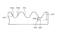
- the top portion 11 ⁇ / b> P of the quadrangular pyramid has a pointed shape, but this may have a rounded shape like the top portion 61 ⁇ / b> P of the concave portion 613 shown in FIG. 5.
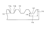
- a flat portion 71P may be provided at the top of the pyramid as in the concave portion 713 shown in FIG. 6 to form a flat chamfered shape.
- the height difference 61R between the top 61P and the top 61Q when the pyramid has a rounded and sharp shape is as follows:
- the pyramid can be 20% or less of the height 61S of the pyramid when the pyramid has a rounded and sharp shape.
- the height of the flat portion 71P and the top 71Q when the top of the pyramid is not flat but sharp.
- the difference 71R can be 20% or less of the height 71S of the pyramid when the apex of the pyramid is not flat but sharp.
- the depth of the concave portion in the concavo-convex structure is not particularly limited, but the average roughness of the center line measured on the surface on which the concavo-convex structure is formed along various directions (various directions in a plane parallel to the device light exit surface).
- the maximum value (Ra (max)) can be in the range of 1 to 50 ⁇ m.
- the thickness of the uneven structure layer is reduced, so that the flexibility of the multilayer body is increased. Handling of the multilayer body in the manufacturing process of the device is facilitated.
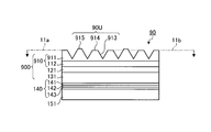
- the difference between the depth 16D of the recess shown in FIG. 4 and the thickness 16E of the concavo-convex structure layer 111 is preferably 0 to 30 ⁇ m.
- the angle formed by the inclined surface of the recess and the light exit surface of the device is preferably 40 to 70 °, and more preferably 45 to 60 °.
- the apex angle (angle 11N in FIG. 4) is preferably 60 to 90 °.
- the angle formed by the inclined surface and the light exit surface of the apparatus is large, and specifically, for example, 55 ° or more.
- the angle is 60 ° or more.
- the upper limit of the angle can be about 70 ° in consideration of maintaining the durability of the uneven structure layer.
- the angle of the slope excluding the rounded portion or the chamfered portion, The angle of the slope.
- the surfaces 613a, 613b, 713a, and 713b are inclined surfaces.
- the slopes of the concavo-convex structure need not all have the same angle, and slopes having different angles may coexist within the above range.
- the angle formed between the conical slope and the device light exit surface can be the angle formed between the conical bus and the device light output surface.
- the plurality of recesses can be arranged in any manner on the device light exit surface.
- a plurality of concave portions can be arranged along two or more directions intersecting each other on the device light exit surface. More specifically, they can be arranged along two orthogonal directions like the recesses 113 shown in FIGS.
- a gap between adjacent concave portions is provided in one or more directions among them, and a flat portion can be constituted by the gap.
- a gap between adjacent concave portions is provided in one or more directions among them, and a flat portion can be constituted by the gap.
- gaps with intervals 11J and 11K are provided in both directions X and Y that are orthogonal to each other, and the flat part 114 is configured by the gaps.
- the manufacturing method of the surface light source device of the first aspect of the present invention is not particularly limited, a surface light source device including the light emitting surface structure layer having the concavo-convex structure layer, the base film, the adhesive layer, and the glass substrate exemplified above is manufactured.
- each layer constituting the organic EL element is laminated on one surface of the glass substrate, and thereafter or before that, the multilayer body having the concavo-convex structure layer and the base film on the other surface of the glass substrate is bonded to the adhesive layer. It can manufacture by sticking through.
- Manufacture of a multilayer body having a concavo-convex structure layer and a base film can be carried out by preparing a mold such as a mold having a desired shape and transferring this to a layer of a material forming the concavo-convex structure layer. .
- Method 1 For example, a raw multilayer having a layer of the resin composition A constituting the base film and a layer of the resin composition B constituting the concavo-convex structure layer (the concavo-convex structure has not yet been formed) is coextruded, for example And a method of forming a concavo-convex structure on the surface of the unprocessed multilayer body on the resin composition B side; and (Method 2) applying the resin composition B in a liquid state on the substrate film Then, a method may be mentioned in which a mold is applied to the applied layer of the resin composition B, and the resin composition B is cured in that state to form an uneven structure layer.
- the raw multilayer body can be obtained by, for example, extrusion molding in which the resin composition A and the resin composition B are coextruded.
- An uneven structure can be formed by pressing a mold having a desired surface shape onto the surface of the unprocessed multilayer body on the resin composition B side. More specifically, a long raw multilayer body is continuously formed by extrusion molding, and the raw multilayer body is pressed with a transfer roll and a nip roll having a desired surface shape, thereby continuously. Manufacturing can be performed efficiently.
- the clamping pressure between the transfer roll and the nip roll is preferably several MPa to several tens of MPa.
- the temperature at the time of transfer is preferably Tg or more (Tg + 100 ° C.) or less, where Tg is the glass transition temperature of the resin composition B.
- the contact time between the unprocessed multilayer body and the transfer roll can be adjusted by the film feed speed, that is, the roll rotation speed, and is preferably 5 seconds or more and 600 seconds or less.
- Method 2 it is preferable to use a composition that can be cured by energy rays such as ultraviolet rays as the resin composition B constituting the concavo-convex structure layer.
- energy rays such as ultraviolet rays
- energy rays such as ultraviolet rays
- the shape of the concave portion constituting the device light-emitting surface is not limited to the pyramid shape exemplified as the above-described Embodiment 1-1.
- Embodiment 1-2 shown below It may be a partial shape of a sphere.
- Embodiment 1-2 is a second embodiment according to the first aspect of the present invention. 7 is a top view schematically showing the surface light source device according to Embodiment 1-2, and FIG. 8 shows the surface light source device shown in FIG. 7 as a device light exit surface passing through line 2a in FIG.
- the surface light source device 20 according to Embodiment 1-2 includes the shape of the device light exit surface, that is, the surface of the concavo-convex structure layer 211 in the multilayer body 210 constituting the light exit surface structure layer 200.
- the configuration is the same as that of Embodiment 1-1 except that the shape is different.
- the concave portion 213 formed on the surface of the concavo-convex structure layer 211 has a hemispherical shape, and is continuous in three arrangement directions parallel to the lines 2a, 2b, and 2c at a certain interval on the device light-emitting surface 20U. Are arranged. Lines 2a, 2b and 2c are at an angle of 60 ° to each other. A gap is provided between the adjacent recesses 213 in the directions of the lines 2a, 2b, and 2c, and the gap constitutes a flat portion 214.
- the shape of the concave portion constituting the device light-emitting surface may be a groove shape as in Embodiment 1-3 shown below.
- Embodiment 1-3 is the third embodiment according to the first aspect of the present invention.
- FIG. 9 is a perspective view schematically showing the surface light source device according to Embodiment 1-3.
- the surface light source device 30 according to Embodiment 1-3 is different in the shape of the light exit surface of the device, that is, the shape of the surface of the concavo-convex structure layer 311 in the multilayer body 310 constituting the light exit surface structure layer 300.
- Others have the same configuration as the embodiment 1-1.
- Each of the plurality of recesses 313 formed on the surface of the concavo-convex structure layer 311 has a linear, groove-like shape and has two flat slopes. Therefore, the cross section obtained by cutting the recess 313 along a plane perpendicular to the extending direction of the groove has a triangular shape having two hypotenuses.
- the plurality of recesses 313 are arranged in parallel on the device light exit surface 30U.
- a gap 314 is provided between the adjacent recesses 313, and the gap 314 constitutes a flat portion on the device light exit surface 30U.
- the light is emitted in the same manner as the pyramid-shaped recess in the embodiment 1-1.
- the extraction efficiency can be increased, the change in color depending on the observation angle can be reduced, and the mechanical strength of the light exit surface of the apparatus can be improved.
- the groove-like shape of the recess is not particularly limited as long as it includes an inclined surface, and the cross section exemplified above is not limited to a triangular shape, and can take various shapes.
- the cross-sectional shape of the groove may be another polygonal shape such as a pentagon or a heptagon, or a shape other than a polygon such as a part of a circle.
- the cross-section of the groove is similar to the shape of the pyramid or the top of the cone described above in connection with embodiment 1-1 being modified to a rounded or flat chamfered shape. The shape may be deformed into a shape with rounded vertices or a flat chamfered shape.
- each concave portion constituting the device light-emitting surface is a pyramid shape
- the pyramid shape is not limited to the simple pyramid shape exemplified as Embodiment 1-1,
- each concave portion may have a shape in which a plurality of pyramids are combined.
- Embodiment 1-4 is a fourth embodiment according to the first aspect of the present invention.
- FIG. 10 is a top view schematically showing the surface light source device according to Embodiment 1-4
- FIG. 11 shows the surface light source device shown in FIG. 10 as a device light exit surface passing through line 3a in FIG. It is sectional drawing which shows the cross section cut
- the surface light source device 40 according to Embodiment 1-4 includes the shape of the device light exit surface 40 ⁇ / b> U, that is, in the concavo-convex structure layer 411 in the multilayer body 410 constituting the light exit surface structure layer 400.
- the configuration of the recess 413 is the same as that of the embodiment 1-1 except that the shape of the recess 413 is different from the recess 113 in the embodiment 1-1.
- Each of the plurality of recesses 413 formed on the surface of the concavo-convex structure layer 411 has three types of inclined surfaces 41T, 41U, and 41V having different inclination angles with respect to the device light exit surface.
- 41V has the largest inclination
- the four inclined surfaces 41V constitute a quadrangular pyramid.
- the slope 41U has a smaller slope than the slope 41V
- the slope 41T has a slope smaller than that of the slope 41U.
- the four-sided slope 41U forms a part of the quadrangular pyramid
- the four-sided slope 41T also forms a part of the quadrangular pyramid.
- the recess 413 has a shape in which three types of quadrangular pyramids or a part thereof are combined.
- the flat part 414 located around the recessed part 413 is comprised by the clearance gap provided between the recessed parts in two orthogonal directions similarly to the flat part 114 in Embodiment 1-1.
- the diffusing member is a member that diffuses and transmits incident light provided as a layer constituting part or all of the light-emitting surface structure layer. Met.
- the diffusing member in the surface light source device of the first aspect of the present invention is not limited to this, and is provided at a position farther from the light emitting surface structure layer than the organic EL element, as exemplified in Embodiment 1-5 shown below.
- a member that diffuses and reflects incident light may be used.
- Embodiment 1-5 is a fifth embodiment according to the first aspect of the present invention.
- FIG. 12 is a cross-sectional view showing a cross section of the surface light source device according to Embodiment 1-5 cut along a plane perpendicular to the device light exit surface.
- the surface light source device 50 according to Embodiment 1-5 includes an electrode layer 146 that is a second transparent electrode instead of the reflective electrode 143 as a second electrode layer, and a sealing substrate. Instead of 151, it differs from the embodiment 1-1 in that it has a reflecting member 551 and a reflecting member substrate 552, and is otherwise the same as the embodiment 1-1.
- the reflecting member 551 has a property of reflecting light incident on the reflecting member 551 at the reflecting surface 551U, and the reflecting surface 551U is not flat but has irregularities. Thereby, the reflection member 551 can reflect the incident light in a diffused manner.
- Reflection in a diffused manner on the reflection surface 551U of the reflection member 551 means that at least part of incident light is reflected by non-specular reflection (reflected in a reflection direction different from the reflection direction in specular reflection). That is. As a result, at least part of the light from the light emitting layer 142 is diffused before reaching the device light exit surface 10U.
- the layer constituting part or all of the light exit surface structure layer is a diffusing member.
- the reflecting member 551 is used. Since the same effect as that of the diffusing member in the light emitting surface structure layer is obtained by the reflection of the light in the diffused mode, the effect of the first invention can be obtained without providing the diffusing member in the light emitting surface structure layer. Can be obtained.
- a diffusion member in the light-emitting surface structure layer such as that provided in Embodiment 1-1 may be provided as an additional diffusion member.
- the gap 553 between the reflecting surface 551U of the reflecting member 551 and the second transparent electrode 146 can be filled with an arbitrary material such as a filler or an adhesive that does not significantly impair light transmission.
- air or other gas may be present or a vacuum space may be used if there is no inconvenience such as greatly impairing the durability of the light emitting layer 142.
- the material of the reflecting member 551 is not particularly limited, but the reflecting member 551 can be a member including at least a layer of a substance having a property of reflecting incident light, such as a metal such as aluminum or silver. More specifically, a reflective member having fine irregularities can be formed by forming one or a plurality of such metal layers on a substrate having a fine irregular structure. Alternatively, a reflective layer having fine irregularities can be obtained by forming a metal layer on a flat substrate and then processing the metal layer. Alternatively, a reflective member having fine irregularities can be obtained by forming a metal layer on a flat resin substrate and then bending the resin substrate.
- the reflecting member may have a structure in which a functional layer such as an inorganic thin film or an organic thin film is laminated on the surface of the metal layer for the purpose of improving adhesion, corrosion resistance, scratch resistance, or the like.
- the material of the reflecting member 551 is not limited to metal, and for example, a diffusion plate made of an arbitrary material having a white surface may be used to reflect the incident light in a diffused manner.
- Embodiment 1-6 when the quadrangular pyramids are arranged along two directions of the light emitting surface of the device, the flat portion has a gap between the adjacent quadrangular pyramids in both the two directions.
- the present invention is not limited to this, and for example, a gap may be provided in only one of the two directions as in the following Embodiment 1-6.
- Embodiment 1-6 is a sixth embodiment according to the first aspect of the present invention.
- FIG. 13 is a top view schematically showing the surface light source device according to Embodiment 1-6
- FIG. 14 shows the surface light source device shown in FIG. 13 as a device light exit surface passing through line 4a in FIG. It is sectional drawing which shows the cross section cut
- the surface light source device 80 according to Embodiment 1-6 includes the shape of the device light exit surface 80U, that is, the surface of the concavo-convex structure layer 811 in the multilayer body 810 constituting the light exit surface structure layer 800. Otherwise, the configuration is the same as that of Embodiment 1-1.
- Each of the concave portions 813 formed on the surface of the concavo-convex structure layer 811 has the same shape as the concave portion 113 in the embodiment 1-1, but the gap between the concave portions 813 is a direction perpendicular to the line 4a in FIG. As a result, a flat portion 814 extending in a direction parallel to the line 4a is formed.
- the abrasion resistance when the device light emitting surface is scratched along a certain direction (for example, a direction parallel to the extending direction of the flat portion 814) is relatively large. While the light extraction efficiency can be improved, the light extraction efficiency can be improved.
- the height of the boundary portion 815 between the adjacent concave portions 813 and the height of the flat portion 814 are the same as the shape of the concave portion 813, but the height of the boundary portion 815 is the height of the flat portion 814. May be different.
- the shape of the recess 813 is only a quadrangular pyramid has been taken here, other shapes may be used.
- it can also be set as the structure with which the some ridge roof-like recessed part 816 was located in a line. Note that the concavo-convex structure layer 821 shown in FIG.
- the concavo-convex structure layer 811 according to Embodiment 1-6 is a modification of the concavo-convex structure layer 811 according to Embodiment 1-6, and is the same as the concavo-convex structure layer 811 according to Embodiment 1-6 except that the shape of the recesses is different. It has the composition of.
- the flat portion on the concavo-convex structure layer has a difference in height (that is, the height in a state where the device light-emitting surface is placed parallel to the horizontal direction and upward).
- the first invention is not limited to this, and there is a difference in the height of the flat portion, for example, as in the following Embodiment 1-7. It may be.
- Embodiment 1-7 is a seventh embodiment according to the first aspect of the present invention.
- 16 is a top view schematically showing the surface light source device according to Embodiment 1-7
- FIG. 17 shows the device light output through the surface light source device shown in FIG. 16 along the line 11a-11b in FIG. It is sectional drawing which shows the cross section cut
- the surface light source device 90 according to Embodiment 1-7 includes the shape of the device light exit surface 90 ⁇ / b> U, that is, the surface of the concavo-convex structure layer 911 in the multilayer body 910 constituting the light exit surface structure layer 900. Otherwise, the configuration is the same as that of Embodiment 1-1.
- Each of the concave portions 913 formed on the surface of the concavo-convex structure layer 911 has substantially the same shape as the concave portion 113 in Embodiment 1-1, but between the concave portions 913, a flat portion 914 having a low height and a height are provided. Two types of flat portions, ie, a high flat portion 915, are provided, and the flat portions 914 and 915 are connected by an inclined surface 91W.
- two rows of flat portions 914 and one row of flat portions 915 are alternately arranged, whereby the light-emitting surface structure layer 900 has two flat portions 914 and one flat portion 915 in its cross section.
- the repeating unit consisting of the slopes (including the slope 91W) of the three recesses 913 existing between them. In addition to the cross section passing through the lines 11a and 11b shown in FIG. 16, this repetition can occur in a cross section perpendicular to the line and perpendicular to the device light exit surface.
- the scratch resistance of the device light exit surface is slightly reduced, but a favorable effect is produced that rainbow unevenness when the device light exit surface is observed can be suppressed.
- the surface light source device is manufactured by designing the device light exit surface so that there is no difference in height in the flat portion, an error occurs in the height of the flat portion based on the error in forming the flat portion. Interference occurs in the light from the device light exit surface (that is, one or both of the light emitted from the device and the reflected light of the external light from the device light exit surface), and rainbow unevenness may occur.
- the occurrence of interference is prevented and rainbow unevenness is suppressed by daringly setting the dimensional difference in height between the two types of flat portions 914 and 915 to be a dimensional difference that exceeds the difference that causes light interference.
- the dimensional difference exceeding the difference causing interference may be, for example, a dimensional difference of 0.62 times or more, preferably 1.5 times or more of the center wavelength of light emitted from the surface light source device.
- a predetermined difference (a dimensional difference exceeding a difference that causes interference) is provided in the height of the flat portion. For example, the height of the flat portion is aligned, and the depth of the concave portion is set.
- a predetermined difference (a dimensional difference exceeding a difference causing interference) may be provided, and in this case, the same effect as described above can be obtained. Moreover, you may provide a difference in both the height of a flat part, and the depth of a recessed part.
- the structure which provides a predetermined difference in a flat part or a recessed part is not applied only to this embodiment, but can be applied to all the embodiments in the scope of the present invention.
- Embodiment 1-8 In the surface light source device of the first aspect of the present invention, instead of using only one surface of the surface light source device as the device light-emitting surface, both surfaces may be used as the device light-emitting surface as in the following Embodiment 1-8, for example.
- Embodiment 1-8 is an eighth embodiment according to the first aspect of the present invention.
- FIG. 18 is a cross-sectional view schematically showing a cross section of the surface light source device according to Embodiment 1-8 taken along a plane perpendicular to the device light exit surface.
- the surface light source device 1000 according to Embodiment 1-8 includes an electrode layer 146 that is a second transparent electrode instead of the reflective electrode 143, and the light emission instead of the sealing base material 151.
- the other points are the same as those in the embodiment 1-1.
- an arbitrary substance such as a filler or an adhesive may exist between the light emitting surface structure layer 100 on the lower side in the drawing and the second transparent electrode 146, or a void exists. May be. As long as there is no inconvenience such as greatly impairing the durability of the light emitting layer 142, air or other gas may be present in the space, or the space may be evacuated.
- the second electrode layer 146 is a transparent electrode, the light from the light emitting layer 142 passes through the first electrode layer 141 and the second electrode layer 146 and is emitted from both the upper and lower devices in the figure. Light exits from the surface 10U. Even when light is emitted from both the front surface and the back surface, as in Embodiment 1-1, the light extraction efficiency can be increased and the change in color depending on the observation angle can be reduced. In addition, the mechanical strength of the light exit surface of the device can be improved.
- the surface light source device 1000 of the present embodiment normally, light incident on one device light exit surface 10U is transmitted through the surface light source device 1000 and emitted from the other device light exit surface 10U. Therefore, the opposite side can be seen with the naked eye through the surface light source device 1000, and a see-through surface light source device can be realized, so that the design can be diversified.
- the light exit surface structure layer 100 may be provided on the surface of the first electrode layer 141, and the light exit surface structure layer 200 may be provided on the surface of the second electrode layer 146.
- the lighting apparatus of the first invention and the backlight device of the first invention both include the surface light source device of the first invention.
- the lighting fixture of the first aspect of the present invention has the surface light source device of the first aspect of the present invention as a light source, and can further include arbitrary components such as a member that holds the light source and a circuit that supplies power.
- the backlight device of the first aspect of the present invention has the surface light source device of the first aspect of the present invention as a light source, and further includes a housing, a circuit for supplying electric power, a diffuser plate for making light emitted more uniform, Arbitrary components, such as a diffusion sheet and a prism sheet, can be included.
- the backlight device of the first aspect of the present invention is used as a backlight of a display device such as a liquid crystal display device that displays an image by controlling pixels and a display device that displays a fixed image such as a signboard. it can.
- the light emitting surface structure layer is composed of a concavo-convex structure layer, a base film layer, an adhesive layer, and a glass substrate, but the light emitting surface structure layer is a layer having fewer layers than these. It may be configured from the above, or conversely, an arbitrary layer may be further included in addition to these layers.
- a coating layer may be further provided on the concavo-convex structure layer, and this may define the concavo-convex structure on the device light exit surface.
- the concave portions distributed on the entire surface of the device light-emitting surface are shown as those having only the same shape distributed.
- concave portions having different shapes are mixed on the light-emitting surface of the device. May be.
- pyramid-shaped recesses of different sizes are mixed
- pyramid-shaped recesses and cone-shaped recesses are mixed
- a combination of multiple pyramids and a simple pyramid shape are mixed. It may be.
- the width of the flat portion and the interval between the adjacent flat portions are always constant, but even if the width of the flat portion is narrow and wide, it may be mixed.
- a portion where the interval between the flat portions is narrow and a portion where the flat portion is wide may be mixed.
- a dimensional difference exceeding the difference that causes interference between the emitted light and the reflected light is provided. Unevenness can be suppressed.
- the apparatus which has the same effect as a reflective electrode can be comprised.
- Embodiment 2-1 is the first embodiment according to the second aspect of the present invention.
- FIG. 19 is a longitudinal sectional view for explaining a surface light source device according to Embodiment 2-1.
- the surface light source device 2001 according to the present embodiment has a light emission surface 2040 ⁇ / b> A having a rectangular shape in plan view, and is directly or indirectly on at least one surface of the organic EL element 2020 and the organic EL element 2020.
- a concavo-convex structure body 2040 as a light output side member disposed in the.
- the organic EL element 2020 includes a first electrode layer 2022 constituting a reflective electrode, a light emitting layer 2024, and a second electrode layer 2026 as a transparent electrode in this order, and the first electrode layer 2022 and the second electrode layer A voltage is applied between the electrode layers 2026 to cause the light emitting layer 2024 to emit light, which can be used as a light source.
- Such an organic EL element 2020 can be suitably used for a lighting fixture, a display device, or the like.
- a known layer can be used for the light emitting layer 2024.
- the light-emitting material used for the light-emitting layer 2024 is not limited to one type, and the light-emitting layer is not limited to one layer, and can be a single layer alone or a combination of a plurality of types in order to suit the use as a light source. . Thereby, what emits the light of the color of white or it can be comprised.
- the electrodes of the organic EL element 2020 are not particularly limited, and known ones can be appropriately selected.
- the first electrode layer 2022 is a metal electrode layer.
- the second electrode layer 2026 is a transparent electrode layer. With such a structure, light emitted from the light-emitting layer 2024 passes through the second electrode layer 2026 or is reflected by the first electrode layer 2022, and passes through the light-emitting layer 2024 and the second electrode layer 2026. The light is transmitted and emitted to the outside of the organic EL element 2020.
- the first electrode layer 2022 can also be configured as a transparent electrode layer, and in this case, light can be emitted from both surfaces of the organic EL element.
- the first electrode layer 2022 is a transparent electrode layer
- a reflecting member or a scattering member (for example, a white scattering member disposed via an air layer) is disposed on the side opposite to the light emitting layer 2024 side. It can also be set as the structure to do.
- the organic EL element 2020 includes a hole injection layer, a hole transport layer, an electron transport layer, and an electron injection between the first electrode layer 2022 and the second electrode layer 2026 as necessary. Other layers such as layers and gas barrier layers can be provided.
- the organic EL element 2020 can also include arbitrary components such as wiring for energizing the electrode layers 2022 and 2026 and a peripheral structure for sealing the light emitting layer.
- each electrode layer and each of the layers provided therebetween are not particularly limited, but specific examples include the same examples as those described in the description of the first aspect of the present invention.
- a light-emitting layer that generates a light emission color having a complementary color relationship which is referred to as a laminated type or a tandem type, can be obtained by appropriately combining the above or other light-emitting layers.
- the combination of complementary colors can be yellow / blue, green / blue / red, or the like.
- the uneven structure 2040 is provided on the surface of the second electrode layer 2026.
- the surface of the concavo-convex structure 2040 opposite to the second electrode layer 2026 side is a light exit surface 2040A that emits light to the outside.
- An uneven structure 2041 is formed on the light exit surface 2040A.
- the light exit surface 2040A is a surface parallel to the surface of the light emitting layer 2024 of the organic EL element 2020, and is parallel to the main surface of the surface light source device.
- these surfaces can be non-parallel to the surface of the light emitting layer.
- each component is “parallel” or “vertical” may include an error within a range that does not impair the effects of the second aspect of the present invention. An error of ⁇ 5 ° from a certain angle may be included.
- the uneven structure 2040 includes, for example, a glass substrate 2042 provided on the surface of the second electrode layer 2026, an uneven structure body 2044, and an adhesive layer 2046 for bonding the substrate 2042 and the uneven structure body 2044.
- the concavo-convex structure main body 2044 includes a base material 2045 and a concavo-convex structure layer 2047 as a light distribution distribution converter provided on the surface of the base material 2045.
- one or more of the substrate 2042, the base material 2045, the adhesive layer 2046, and the concavo-convex structure layer 2047 are composed of a composition including particles that impart light diffusibility, and the light diffusibility.
- the layer having the light from the light emitting layer 2024 is diffused and transmitted or reflected, so that the layer functions as the diffusion portion of the second aspect of the present invention.
- the substrate 2042 functions as a plate material that provides rigidity for suppressing the deflection of the surface light source device 2001. Further, since the substrate 2042 has excellent performance for sealing the organic EL element 2020 and can easily form the layers constituting the organic EL element 2020 in order in the manufacturing process, the surface light source device 2001 is provided. There is an advantage that the durability can be improved and the manufacturing can be facilitated.
- the thickness of the substrate 2042 is not particularly limited, but is preferably 0.1 to 5 mm.
- the base material 2042 is made of glass, but may be made of resin. In this case, the refractive index of the resin and glass constituting the substrate 2042 can be 1.4 to 2.
- the substrate 2045 can be composed of a composition containing a transparent resin. That the transparent resin is “transparent” means that it has a light transmittance suitable for use in an optical member.
- each layer constituting the light output side member can have a light transmittance suitable for use in the optical member, and the light output side member as a whole has a total light transmittance of 80% or more. It can have.
- Examples of the transparent resin are the same as those described in the section of the light emitting surface structure layer in the description of the first invention.
- the concavo-convex structure layer 2047 is located in the outermost layer on the light emission surface side of the surface light source device 2001, and the surface opposite to the substrate 2045 is a light emission surface 2040A.
- the concavo-convex structure layer 2047 has a concavo-convex structure including a plurality of concave portions 2048 including inclined surfaces and a flat portion 2049 formed in a planar shape that is located around the concave portions 2048 and separates the adjacent concave portions 2048.
- a material constituting the concavo-convex structure layer 2047 the same material as the base material 2045 described above can be employed.
- the light exit surface is defined by the uneven structure.
- the “slope” is a surface that forms an angle that is not parallel to the light exit surface.
- the surface on the flat portion can be a surface parallel to the light exit surface.
- the ratio of the area occupied by the flat portion 2049 to the total of the area occupied by the flat portion 2049 and the area occupied by the concave portion 2048 (hereinafter referred to as “flat portion ratio”). ”) Is appropriately adjusted, the light extraction efficiency of the surface light source device 2001 can be improved. Specifically, by setting the flat portion ratio to 10 to 75%, good light extraction efficiency can be obtained, and the mechanical strength of the light exit surface 2040A can be increased.
- Each of the plurality of recesses 2048 is a depression having a regular quadrangular pyramid shape.
- the inclined surface 2048 ⁇ / b> A constituting each concave portion 2048 is the same isosceles triangle.
- the plurality of recesses 2048 are arranged along two arrangement directions perpendicular to each other at a constant interval, and at this time, the respective recesses 2048 face each other in the same direction.
- the angle formed by the inclined surface 2048A constituting each of the recesses 2048 and the flat portion 2049 can be set to 60 °, for example.
- the apex angle of the regular quadrangular pyramid constituting the recess 2048 is 60 °.
- the angle between the inclined surface of the concave portion and the flat portion should be 40 to 70 ° on average from the viewpoint that the light extraction efficiency can be further increased while minimizing the change in color depending on the observation angle. preferable.
- a material having a high hardness at the time of curing is preferable from the viewpoint of easily forming the concavo-convex structure on the light exit surface and easily obtaining scratch resistance of the concavo-convex structure.
- a material having a pencil hardness of HB or higher is preferable, and a material of H or higher is more preferable. The material which becomes 2H or more is more preferable.
- a certain degree of flexibility may be used in order to facilitate handling of the concavo-convex structure main body 2044 when forming the concavo-convex structure layer 2047 and / or after forming the concavo-convex structure main body 2044. Some are preferred. By combining such materials, it is possible to obtain a concavo-convex structure main body 2044 that is easy to handle and has excellent durability. As a result, a high-performance surface light source device can be easily manufactured.
- Such a combination of materials can be obtained by appropriately selecting the transparent resin exemplified above as a resin constituting each material.
- an ultraviolet curable resin such as acrylate is used as the transparent resin constituting the material of the concavo-convex structure layer 2047, while the alicyclic olefin polymer film is used as the transparent resin constituting the material of the substrate 2045. (Zeonor film, etc., described later) or a polyester film can be used, whereby a preferable combination of materials can be obtained.
- the refractive index difference between the base material 2045 and the uneven structure layer 2047 can be made as small as possible.
- the difference in refractive index is preferably within 0.15, more preferably within 0.05. preferable.
- the composition serving as a material of a layer serving as a constituent element such as the base material 2045 and the concavo-convex structure layer 2047 can include particles, which will be described later, imparting light diffusibility when the layer constitutes a diffusion portion.
- the base material 2045 and the concavo-convex structure layer 2047 also serve as a diffusion portion.
- the composition may contain optional components as necessary. Examples of the optional component include the same examples as described in the section of the light exit surface structure layer in the description of the first aspect of the present invention.
- the thickness of the uneven structure layer 2047 is not particularly limited, but is preferably 1 to 70 ⁇ m.
- the thickness of the concavo-convex structure layer 2047 is the distance between the surface on the substrate side where the concavo-convex structure 2041 is not formed and the flat portion 2049 of the concavo-convex structure 2040.
- the thickness of the substrate 2045 is preferably 20 to 300 ⁇ m.
- an adhesive including a pressure-sensitive adhesive
- an adhesive having a refractive index close to that of the substrate 2045 or the uneven structure layer 2047 and transparent can be used as appropriate.
- the adhesive include an acrylic adhesive (pressure-sensitive adhesive).
- the thickness of the adhesive layer 2046 is preferably 5 to 100 ⁇ m.
- part or all of the layers constituting the concavo-convex structure 2040 is a layer that diffuses light, so that part or all of these layers are diffused portions.
- the material for the layer that diffuses light include a material containing particles and a material that is an alloy resin that diffuses light by mixing two or more kinds of resins. From the viewpoint that light diffusibility can be easily adjusted, a material containing particles, particularly a resin composition containing particles, is particularly preferable.
- the particles are the same as the particles described in the section of the diffusing member in the first description of the present invention. Therefore, for example, the material, content ratio, particle size, refractive index, and the like of the particles are the same as the particles described in the section of the diffusing member in the first description of the present invention.
- a layer constituting part or all of the concavo-convex structure is used as the diffusion part
- which of the layers constituting the concavo-convex structure is used as the diffusion part is not particularly limited, and can be selected from various viewpoints. can do.
- a layer containing a transparent resin is preferably used as the diffusion portion.
- the concavo-convex structure layer is preferably a material having a high hardness as described above.
- a layer other than the concavo-convex structure layer that can easily impart plastic deformation for example, a base material and / or an adhesive layer is provided, and this layer is diffused.
- the manufacturing process can be facilitated by using a layer that does not involve a heating process of a material such as a transparent resin in the manufacturing process as a diffusion part.
- a layer that does not involve a heating process of a material such as a transparent resin in the manufacturing process as a diffusion part.
- the adhesive layer is a diffusion portion.
- the refractive index of such a diffusion part is not particularly limited, but is preferably 1.45 to 2, more preferably 1.6 to 2, and still more preferably 1.7 to 2. It is preferable that the layer on the light emission side of the diffusion part has a refractive index smaller than that of the diffusion part, but the refractive index of the light emission side of the diffusion part can be selected by increasing the refractive index of the diffusion part as described above. Since the width of is widened, the selectivity of the material can be expanded. *
- a layer other than the concavo-convex structure layer, the base material, the adhesive layer, and the glass substrate may be additionally provided in the concavo-convex structure, and the additional layer may be used as a diffusion portion.
- the additional layer may be used as a diffusion portion.
- the concavo-convex structure layer and the base film layer between the adhesive layer and the glass substrate, the surface on the light emitting layer side of the glass substrate, etc. (for example, between the electrode layer constituting the light emitting layer and the glass substrate) can be formed.
- both the additional layer and the concavo-convex structure layer, the base material, the adhesive layer, and one or more layers of the glass substrate can be used as the diffusion portion.
- the degree of diffusion is not particularly limited, but as an example, the diffusion portion is part or all between the concavo-convex structure layer and the adhesive layer
- the total light transmittance of the portion from the concavo-convex structure layer to the adhesive layer in a state where the concavo-convex structure layer has no surface unevenness is 70 to 95% from the viewpoint that a sufficient effect of eliminating color unevenness can be secured. Is more preferable, and 73 to 90% is more preferable.
- the surface light source device 2001 of the second aspect of the present invention has the above-described configuration so that the displacement of at least one of the x-coordinate and the y-coordinate of the chromaticity coordinate in all hemispherical directions on the light exit surface 2040A has the above-described configuration. Compared with the case where it does not take, it can be made small, for example, can be reduced to half. For this reason, in the surface light source device 2001, a change in color due to an observation angle can be suppressed.
- a spectral radiance meter is installed on the normal line (front) of the light output surface 2040A, and the light output is obtained when the normal direction is set to 0 °.
- the chromaticity coordinates can be calculated from the emission spectrum measured in each direction, so that the displacement can be calculated.
- the concavo-convex structure layer 2047 formed on the concavo-convex structure main body 2044 has the light distribution of the incident light when the light emitted from the organic EL element 2020 enters the concavo-convex structure 2041.
- the difference between the chromaticity of the light emitted from 2040A along the normal direction of the light exit surface 2040A and the chromaticity of the light emitted from the light output surface 2040A along the oblique direction intersecting the normal direction is reduced. It functions as a light distribution distribution conversion unit for converting to. Since such concavo-convex structure 2041 can adjust the chromaticity that varies depending on the observation direction, the diffusion effect in the diffusion portion described above can be supplemented.
- the amount of particles added to the layer constituting the diffusion portion for example, This can be reduced as compared with the prior art.
- diffusion part can be made thin or lightweight, it can contribute also to thickness reduction, size reduction, etc. of the surface light source device 2001.
- the manufacturing method of the surface light source device 2001 which concerns on this embodiment is not specifically limited,
- each layer which comprises an organic EL element is laminated
- the concavo-convex structure main body can be formed by preparing a mold such as a mold having a desired shape and transferring the mold to a material layer for forming the concavo-convex structure layer. More specific methods include, for example, Method 1 and Method 2 mentioned in the section of the production method in the description of the first invention.
- Both the lighting apparatus of the second invention and the backlight device of the second invention include the surface light source device.
- the lighting fixture of the second aspect of the present invention has the surface light source device of the second aspect of the present invention as a light source, and can further include arbitrary components such as a member that holds the light source and a circuit that supplies power.
- the backlight device of the second aspect of the present invention has the surface light source device of the second aspect of the present invention as a light source, and further includes a housing, a circuit for supplying power, a diffusion plate for making light emitted more uniform, Arbitrary components, such as a diffusion sheet and a prism sheet, can be included.
- the use of the backlight device of the second aspect of the present invention is to be used as a backlight of a display device for controlling a pixel to display an image, such as a liquid crystal display device, and a display device for displaying a fixed image such as a signboard. it can.
- Embodiment 2-2 is a second embodiment according to the second aspect of the present invention. Note that the same or corresponding components as those in Embodiment 2-1 are denoted by the same reference numerals, and description thereof is omitted or simplified.
- FIG. 20 is a longitudinal sectional view for explaining a surface light source device according to Embodiment 2-2. As shown in FIG. 20, the surface light source device 2002 according to the present embodiment has a light emission surface 2040 ⁇ / b> A having a rectangular shape in plan view, and is arranged in contact with at least one surface of the organic EL element 2020 and the organic EL element 2020. The light emission side member 2060 is provided.
- the light output side member 2060 includes a selective reflection member 2062, a glass substrate 2042, and a diffusion layer 2070 as a diffusion portion disposed between the selective reflection member 2062 and the glass substrate 2042.
- the selective reflection member 2062 includes a base film 2064 and a selective reflection layer 2066 provided on the surface of the base film 2064.
- the diffusion layer 2070 is a layer that diffuses light from the organic EL element 2020.
- the material constituting the diffusion layer include a material containing particles and a material made of alloy resin that diffuses light by mixing two or more kinds of resins. From the viewpoint that light diffusibility can be easily adjusted, a composition containing particles is preferable, and a resin composition containing particles is particularly preferable.
- the selective reflection layer 2066 is a layer having a property of transmitting specific polarized light and reflecting or absorbing other polarized light in a certain wavelength band.
- the selective reflection band is a wavelength band in which the selective reflection layer has such properties.
- the base material 2064 can be configured similarly to the base material 2045 described above.
- the selective reflection layer 2066 since the selective reflection layer 2066 usually has different selective reflection performance depending on the wavelength, the configuration is appropriately selected according to the emission intensity peak of the light emitting layer.
- a light emitting layer having two or more emission intensity peaks can be adopted, and one or more of the two or more emission intensity peaks have a wavelength in the range of 500 nm to 650 nm. Is preferred.
- An example of the spectrum of the light emitting layer having such a light emission intensity peak is shown in FIG.
- the spectrum shown in FIG. 21 has two peaks at wavelengths of 480 nm and 575 nm.
- Such two or more emission intensity peaks can be obtained by forming the light emitting layer as a laminate of a plurality of layers having different emission colors or a mixed layer in which a different dye is doped in a certain dye layer.
- the selective reflection layer 2066 includes at least one peak wavelength of the emission intensity peak in the selective reflection band of transmitted light in the front direction.
- the selective reflection layer may include at least one of the wavelengths 480 nm and 575 nm in the selective reflection band of transmitted light in the front direction. it can.
- the selective reflection band refers to the transmittance ( ⁇ ) [%] when the maximum transmittance in the visible light region 380 to 780 nm is a [%] and the minimum transmittance is b [%]: ⁇ A-transmittance ( ⁇ ) ⁇ / ⁇ ab ⁇ ⁇ 0.3
- the selective reflection layer 2066 has a transmittance T F Y, N in the front direction at a wavelength of 575 nm, an average value T F Y, 60 of a transmittance in the polar angle 60 ° direction at a wavelength of 575 nm, and a transmission in the front direction at a wavelength of 480 nm.
- the rate T F B, N and the average value T F B, 60 of the transmittance in the direction of the polar angle of 60 ° with the wavelength of 480 nm may satisfy the relationship of the formula [1]. Since the selective reflection layer 2066 has such a selective reflection band, a change in color depending on the observation angle can be reduced. (T F Y, 60 / T F Y, N)> (T F B, 60 / T F B, N) formula (1)
- the selective reflection layer 2066 has one or more selective reflection bands in a wavelength range of 500 nm to 650 nm as a selective reflection band of transmitted light in the front direction. Further, preferably, the selective reflection layer 2066 has one or more selections within a wavelength range of 400 nm to 600 nm as a selective reflection band of transmitted light in a polar angle direction of 60 °, that is, a direction that forms an angle of 60 ° with the front direction. Has a reflection band.
- FIG. 22 shows an example of the selective reflection characteristic having the selective reflection band described above in relation to the spectrum of the light emitting element shown in FIG.
- the selective reflection characteristic of transmitted light in an angle of 0 ° that is, in the front direction
- the light is most reflected at a wavelength of 575 nm
- the selective reflection band of transmitted light in the front direction is 525 nm or more and 635 nm or less.
- the maximum absorption wavelength shifts to the short wavelength side, thereby satisfying the above equation [1], and further in the polar angle 60 ° direction, the maximum absorption wavelength is 490 nm, and the selective reflection band is 580 nm. It is as follows.
- FIG. 25 shows the surface light source device according to the second aspect of the present invention shown in FIG. 20, in which an element having the spectrum shown in FIG. 21 is used as the light emitting element, and the selective reflection layer 2066 has the selective reflection characteristics shown in FIG. 6 is a graph showing a light distribution of blue light having a wavelength of 480 nm and yellow light having a wavelength of 575 nm emitted from the light exit surface 2040A when using the light source.
- FIG. 24 is a graph showing a light distribution when a light distribution of blue light and yellow light emitted from a glass substrate is observed without providing the diffusion layer 2070.
- FIG. 23 is a graph showing a light distribution when observed without any of the diffusion layer 2070 and the selective reflection member 2062.
- the light emitted from the glass substrate 2042 has a difference in light distribution between blue light and yellow light.
- the light exits through the selective reflection member 2062.
- the deviation of the light emitted from 2040A is reduced.
- the selective reflection member 2062 has a light distribution distribution of the light emitted from the organic EL element 2020, the chromaticity of the light emitted along the normal direction of the light output surface 2040A, and an oblique direction intersecting the normal direction. Is functioning as a light distribution distribution conversion unit for conversion so that the difference from the chromaticity of the light emitted from the light exit surface 2040A along the line becomes small.
- the light emitted from the glass substrate 2042 has a difference in light distribution between blue light and yellow light
- the diffusion layer 2070 and the selective reflection member 2062 are separated.
- the light transmitted through the light exit surface 2040A is further reduced in the deviation.
- the selective reflection member 2062 can suppress the color unevenness based on the observation angle, and the diffusion layer 2070 can further suppress the color unevenness.
- the effect of eliminating color unevenness can be further enhanced as compared with the case where only the diffusion layer 2070 is used or the case where only the selective reflection member 2062 is used.
- the degree of the diffusion effect by the diffusion layer 2070 can be suppressed to a low level, whereby the ratio of addition of, for example, diffusion particles can be suppressed, and the thickness of the diffusion layer can be reduced.
- a part of the light generated from the light emitting layer 2024 is directly transmitted through the second electrode layer 2026, and the other part is reflected by the first electrode layer 2022 before being reflected.
- the second electrode layer 2026 is transmitted.
- Light that has passed through the second electrode layer 2026 passes through the glass substrate 2042, the diffusion layer 2070, the selective reflection layer 2066, and the base film 2064, and is emitted. Further, light reflected downward in the drawing at the interface between the light emitting layer 2024 and the glass substrate 2042 is reflected at the first electrode layer 2022 or another interface and then emitted. Since there is light emitted through such various paths, light interference occurs.
- the increase / decrease in light due to interference differs depending on the wavelength, and as a result, the relationship between the observation angle and the luminance differs depending on the wavelength of the light, resulting in a change in color depending on the observation angle.
- the selective reflection layer 2066 is provided on one surface of the base film 2064. However, even when the selective reflection layer 2066 is provided on both surfaces of the base film 2064, the same advantage can be obtained. it can.
- the selective reflection layer 2066 has the selective reflection band
- any material may be used and selective reflection of any principle may be performed.
- the thing containing a polarization separation sheet can be mentioned.
- the selective reflection layer has a circularly polarized light separating sheet
- the selective reflection layer transmits only specific circularly polarized light and reflects other light (other circularly polarized light, linearly polarized light, etc.) in the selective reflection band. .
- the circularly polarized light separating sheet examples include a layer containing a resin having cholesteric regularity.
- a composition capable of exhibiting a cholesteric liquid crystal phase (cholesteric liquid crystal composition) is applied to a transparent resin substrate to obtain a liquid crystal layer, and then cured by at least one light irradiation and / or heating treatment.
- the circularly-polarized-light separation sheet which can be mentioned can be mentioned.
- the cholesteric liquid crystal composition a composition containing a rod-like liquid crystal compound that can be cured by itself or with other substances can be used.
- a rod-like liquid crystal compound having a refractive index anisotropy ⁇ n of 0.10 or more and having at least two or more reactive groups in one molecule can be given.
- the method for producing the cholesteric liquid crystal composition is not particularly limited, and can be produced by mixing the above essential components and optional components.
- the cholesteric liquid crystal composition is applied to a base film 2064 to obtain a liquid crystal layer, and then at least one time of light irradiation and / or heating.
- the method of hardening by a process is mentioned.
- the material of the substrate film 2064 is not particularly limited, and a substrate having a thickness of 1 mm and a total light transmittance of 80% or more can be used.
- alicyclic olefin polymers, chain olefin polymers such as polyethylene and polypropylene, triacetyl cellulose, polyvinyl alcohol, polyimide, polyarylate, polyester, polycarbonate, polysulfone, polyethersulfone, modified acrylic polymer, epoxy resin Examples thereof include a single layer or laminated film made of a synthetic resin such as polystyrene or acrylic resin.
- an alicyclic olefin polymer or a chain olefin polymer is preferable, and an alicyclic olefin polymer is particularly preferable from the viewpoint of transparency, low hygroscopicity, dimensional stability, lightness, and the like.
- particles or the like that impart light diffusibility can also be added to the base film 2064.
- the base film 2064 is composed of a composition containing particles that impart light diffusibility, and also serves as a diffusion portion, so that the thickness of the diffusion layer 2070 can be reduced. There is.
- the base film can have an alignment film as required.
- the cholesteric liquid crystal composition applied thereon can be aligned in a desired direction.
- the thickness of the alignment film may be any film thickness that can achieve the desired alignment uniformity of the liquid crystal layer, and is preferably 0.001 to 5 ⁇ m, and more preferably 0.01 to 2 ⁇ m.
- coating of the liquid-crystal composition to the said base film can be performed by well-known methods, such as reverse gravure coating, direct gravure coating, die coating, and bar coating. Before curing the coating layer obtained by the coating, an orientation treatment can be performed as necessary. The alignment treatment can be performed, for example, by heating the coating layer at 50 to 150 ° C. for 0.5 to 10 minutes. By performing the alignment treatment, the cholesteric liquid crystal layer can be aligned well.
- a cured liquid crystal layer that is a cured product of the cholesteric liquid crystal composition can be obtained by curing the cholesteric liquid crystal composition after performing an alignment treatment as necessary.
- the curing step can be performed by a combination of one or more light irradiations and a heating treatment.
- the heating conditions are, for example, a temperature of 40 to 200 ° C., preferably 50 to 200 ° C., more preferably 50 to 140 ° C., and a time of 1 second to 3 minutes, preferably 5 to 120 seconds. it can.
- the light used for light irradiation in the second invention includes not only visible light but also ultraviolet rays and other electromagnetic waves.
- the light irradiation can be performed, for example, by irradiating light having a wavelength of 200 to 500 nm for 0.01 second to 3 minutes.
- a weakly irradiated ultraviolet ray of 0.01 to 50 mJ / cm 2 and heating may be alternately repeated a plurality of times to obtain a circularly polarized light separating sheet having a wide reflection band.
- a relatively strong ultraviolet ray of 50 to 10,000 mJ / cm 2 is irradiated to completely polymerize the liquid crystalline compound to form a cured liquid crystal layer. it can.
- the expansion of the reflection band and the irradiation with strong ultraviolet rays may be performed in the air, or a part or all of the process may be performed in an atmosphere in which the oxygen concentration is controlled (for example, in a nitrogen atmosphere). .
- the step of applying and curing the cholesteric liquid crystal composition on the transparent resin substrate is not limited to one time, and repeating the application and curing a plurality of times to form two or more cured liquid crystal layers. You can also.
- the dry film thickness of the cured liquid crystal layer is preferably 0.5 ⁇ m to 10.0 ⁇ m, more preferably 1.0 ⁇ m to 5.0 ⁇ m. If the dried film thickness of the cured liquid crystal layer is thinner than 0.5 ⁇ m, sufficient selective reflection performance cannot be obtained. Conversely, if it is thicker than 10.0 ⁇ m, light absorption in the cured liquid crystal layer increases, which is not preferable.
- the dry film thickness refers to the total film thickness of each layer when the cured liquid crystal layer is two or more layers, and the film thickness when the cured liquid crystal layer is one layer.
- the laminated structure having the base film 2064 and the selective reflection layer 2066 is obtained by the above process. By attaching this to the glass substrate 2042 via the diffusion layer 2070, the surface light source device 2002 shown in FIG. 20 can be obtained.
- the lighting apparatus of the second aspect of the invention and the backlight device of the second aspect of the invention both include the surface light source device as in the embodiment 2-1, and have the same effects as those in the embodiment 2-1. Can do.
- the concave-convex structure includes a concave portion.
- the present invention is not limited to this, and the concave-convex structure may include a convex portion.
- the same flat portion may be provided between adjacent convex portions, or may not be provided.
- the shape of the recess is a regular quadrangular pyramid, but a polygonal pyramid such as a triangular pyramid or an octagonal pyramid, a conical shape, a polygonal frustum shape, a frustoconical shape, a hemispherical shape, or a groove shape. Or a combination of these.
- the concavo-convex structure is configured to include a polygonal pyramid shape or a polygonal frustum shape
- the slope of each polygonal pyramid does not necessarily have to be a strict plane, and has a curved surface shape including some fluctuations. It may be formed.
- the concavo-convex structure includes a cone
- the generatrix of the cone is not necessarily a strict straight line but may be a curved line including a slight fluctuation.
- the apex angle part may be a round shape even if it is a convex shape or a concave shape.
- it is not limited to a so-called straight cone, and may be an oblique cone.
- the plurality of recesses are all the same shape, but recesses having different shapes may be mixed.
- recesses having different shapes may be mixed.
- pyramid-shaped recesses of different sizes are mixed
- pyramid-shaped recesses and cone-shaped recesses are mixed
- a combination of multiple pyramids and a simple pyramid shape are mixed. It may be.
- the concave portions are arranged along two directions orthogonal to each other.
- the concave portions may be arranged in directions not orthogonal to each other, or may be arranged along one or more directions.
- the flat part was provided in either direction of the said 2 direction between adjacent recessed parts, you may provide only in any one direction, and does not need to provide in both directions.
- the configuration in which the flat portion is provided has an advantage that both good light extraction efficiency and mechanical strength of the light output surface can be achieved.
- the selective reflection layer is a layer containing a resin having cholesteric regularity, but is not limited thereto, and may be a dielectric multilayer film. Examples thereof include a band-pass filter that exhibits strong reflection or transmission characteristics at a specific wavelength using TiO 2 as a material and SiO 2 as a low refractive index material.
- the characteristics of these selective reflection layers are common in that the wavelength range showing the selective reflection characteristics shifts when the observation angle is changed, and the transmittance of light having a wavelength in the visible light range is also common. The characteristics that change with the shift are utilized.
- the surface light source device may further include an arbitrary layer.
- a coating layer may be further provided on the concavo-convex structure layer, and this may define the concavo-convex structure on the light exit surface.
- a sealing substrate may be provided on the surface of the organic EL element opposite to the light exit surface 2040A.
- the concavo-convex structure or the selective reflection member is used as the light distribution distribution conversion unit.
- the present invention is not limited to this.
- a diffractive structure may be used.
- the diffractive structure can strongly diffuse a specific wavelength by selecting an appropriate pitch, and in this case as well, the color unevenness can be further eliminated by combining with another diffusion layer as in the above embodiments. effective.
- the light emission side member was provided only in one surface of the organic EL element 2020, you may provide in both surfaces.
- the first electrode layer described above is also preferably configured as a transparent electrode. Examples of such cases are shown in FIGS.
- FIGS. 26 and 27 are longitudinal sectional views for explaining the surface light source device according to the second embodiment of the present invention.
- a surface light source device 2003 shown in FIG. 26 includes a first electrode 2028 as a transparent electrode instead of the first electrode 2022 as a reflective electrode, and an uneven structure body 2040 on both surfaces of the organic EL element 2020.
- the second embodiment is the same as the embodiment 2-1.
- the surface light source device 2004 shown in FIG. 27 includes a first electrode 2028 as a transparent electrode instead of the first electrode 2022 as a reflective electrode, and the light emitting side on both surfaces of the organic EL element 2020.
- the member 2060 is provided, the other points are the same as those in the embodiment 2-2.
- an arbitrary substance such as a filler or an adhesive may exist between the first electrode 2028 and the substrate 2042, or a gap may exist.
- air or other gas may be present in the space, or the space may be evacuated.
- the first electrode layer 2028 is a transparent electrode
- light from the light-emitting layer 2024 passes through the first electrode layer 2028 and the second electrode layer 2026, and the upper side in the drawing.
- the light exits from both of the light exit surfaces 2040A on the lower side.
- the same effects as those of the embodiment 2-1 and the embodiment 2-2 can be obtained.
- light incident on one light exit surface 2040A normally passes through the surface light source devices 2003 and 2004 and exits from the other light exit surface 2040A. Accordingly, the opposite side can be seen with the naked eye through the surface light source devices 2003 and 2004, and a see-through surface light source device can be realized, so that the design can be diversified.
- the example provided with the same light emission side member (uneven
- the uneven structure 2040 may be provided on the surface of the first electrode 2028 and the light emission side member 2060 may be provided on the surface of the second electrode layer 2026.
- a layer formed of a composition containing particles imparting light diffusibility may be provided on the light exit side of the concavo-convex structure layer 2047 or the selective reflection member 2062, and this layer may be used as a diffusion portion.
- the refractive index of the resin described below is the refractive index after curing.
- C1-1 Formation of organic EL element, production of surface light source device (without multiple layers)
- a reflective electrode layer of 100 nm were formed in this order.
- the hole transport layer to the electron transport layer were all made of an organic material.
- the yellow light emitting layer and the blue light emitting layer have different emission spectra.
- each layer from the transparent electrode layer to the reflective electrode layer is as follows: -Transparent electrode layer; tin-added indium oxide (ITO) Hole transport layer: 4,4′-bis [N- (naphthyl) -N-phenylamino] biphenyl ( ⁇ -NPD) ⁇ Yellow luminescent layer: 1.5% by weight of rubrene added ⁇ -NPD Blue light emitting layer: 10% by weight of iridium complex added 4,4′-dicarbazolyl-1,1′-biphenyl (CBP) -Electron transport layer; phenanthroline derivative (BCP) -Electron injection layer; lithium fluoride (LiF) -Reflective electrode layer: Al
- the transparent electrode layer was formed by a reactive sputtering method using an ITO target, and the surface resistance was 10 ⁇ / ⁇ or less.
- the formation from the hole injection layer to the reflective electrode layer is carried out by placing a glass substrate on which a transparent electrode layer has already been formed in a vacuum evaporation apparatus, and successively using the resistance heating method for the materials from the hole transport layer to the reflective electrode layer. This was done by vapor deposition.
- the system internal pressure was 5 ⁇ 10 ⁇ 3 Pa, and the evaporation rate was 0.1 to 0.2 nm / s.
- a wiring for energization was attached to the electrode layer, and further, the hole transport layer to the reflective electrode layer were sealed with a sealing member to produce a surface light source device (no multi-layer body).
- the obtained surface light source device had a rectangular light exit surface capable of emitting white light from the glass substrate side.
- Example 1-1 The multilayer body 110 prepared by the following procedure was attached to the surface light source device obtained in Comparative Example 1-1, and the surface light source device schematically shown in FIGS. 1 and 2 was produced and evaluated. However, in FIG. 1, an organic EL element 140 having only three layers is schematically illustrated. However, the surface light source device manufactured in this example includes an organic EL element including more light emitting layers. ing.
- the mixture was added at 10% (volume ratio) and stirred to disperse the particles to obtain a resin composition.
- a metal mold having a predetermined shape is pressed onto the coating film of the resin composition, It is a rectangular film having a layer structure of a base film layer 112 and a concavo-convex structure layer 111 by irradiating ultraviolet rays from the base film side with an integrated light quantity of 1000 mJ / cm 2 to form a concavo-convex structure layer on the base film.
- a multilayer body 110 was obtained.
- the concavo-convex structure on the concavo-convex structure layer 111 was composed of a plurality of regular quadrangular pyramid-shaped recesses 113 and a flat part 114 positioned around the recesses, as shown in FIGS.
- the angle (11L, 11M, etc.) formed by the inclined surface forming the recess 113 and the flat portion was 60 °.
- the length of the bottom sides (11E to 11H) of the recess 113 was 16 ⁇ m, and the intervals 11J and 11K of the recess 113 were both 4 ⁇ m, which was a constant interval.
- the bottom side of the recess 113 was parallel to the long side or short side direction of the multilayer body 110.
- the thickness of the uneven structure layer 111 was 34 ⁇ m, and the thickness of the base film layer 112 was 100 ⁇ m.
- the flat portion ratio was 36%.
- the multilayer body 110 obtained in (1-1) was bonded with an adhesive (acrylic resin, refractive index 1). 49, CS9621 manufactured by Nitto Denko Corporation) to obtain a surface light source device including the layer structure of multilayer 110, adhesive layer 121, glass substrate 131, and organic EL element 140.
- the thickness of the adhesive layer was 25 ⁇ m.
- ⁇ Comparative Example 1-2> In preparing the multilayer body 110 of (1-1) above, a multilayer body 110 was prepared in the same manner as in Example 1-1, except that no diffusing agent was added to the material for the uneven structure layer. Furthermore, a surface light source device was obtained.
- the light extraction amount of the surface light source devices of Comparative Example 1-1, Example 1-1, and Comparative Example 1-2 was obtained from the measurement result of the tristimulus Y value, and the light extraction amount of Comparative Example 1-1 was set to 1. The relative amount was determined. As a result, the light extraction amount in Example 1-1 was 1.43, and the light extraction amount in Comparative Example 1-2 was 1.37.
- the surface light source device of Example 1-1 had significantly improved light extraction efficiency as compared with the surface light source device of Comparative Example 1-1 that did not have a concavo-convex structure that increased light extraction efficiency. Further, the surface light source device of Example 1-1 has a greatly improved light extraction amount as compared with the surface light source device of Comparative Example 1-2 which has the same uneven structure as Example 1-1 but does not have a diffusing member. Was recognized.
- Example 1-2 A multilayer body 110 was prepared in the same manner as in Example 1-1 except that the following points were changed, and a surface light source device was obtained.
- no diffusing agent was added to the material for the uneven structure layer.
- the same diffusing agent as used in (1-1) above was added to the acid-modified polyolefin resin (refractive index: 1.49, Cornova MPO-B130C manufactured by Nippon Cima Co., Ltd.) at 10% (volume ratio) in the total amount of the adhesive.
- an adhesive which was used as an adhesive in place of the acrylic adhesive in the above (1-2).
- ⁇ Comparative Example 1-4> In preparation of the multilayer body 110 of (1-1) above, ultraviolet rays are irradiated without pressing the metal mold in forming the concavo-convex structure layer, and as a result, the same material as the concavo-convex structure layer is used instead of the concavo-convex structure layer.
- the light extraction amount of the surface light source devices of Example 1-2, Comparative Example 1-3, and Comparative Example 1-4 was obtained from the measurement result of the tristimulus Y value, and the light extraction amount of Comparative Example 1-1 was 1 The relative amount was determined. As a result, the light extraction amount in Example 1-2 is 1.38, the light extraction amount in Comparative Example 1-3 is 1.29, and the light extraction amount in Comparative Example 1-4 is 1. 24.
- the surface light source device of Example 1-2 had significantly improved light extraction efficiency as compared with the surface light source device of Comparative Example 1-1 that did not have a concavo-convex structure that increased light extraction efficiency.
- the surface light source device of Example 1-2 further has the same concavo-convex structure as that of Example 1-2, but also compared with the surface light source device of Comparative Example 1-3 that does not have a diffusing member. As compared with the surface light source device of Comparative Example 1-4 having the same diffusing member as that of FIG.
- Example 1-1 Scratch resistance> Except that the shape of the metal mold was changed, several multilayers having different concavo-convex structure shapes were obtained in the same manner as in Example 1-1 (1-1). In the obtained multilayer body, the shape of the concave portions was the same, but the flat portion ratio was changed variously by changing the distances 11J and 11K between the concave portions.
- Several obtained multilayered bodies were placed horizontally, and the sapphire needle having a diameter of 2 mm was pressed against the sapphire needle vertically while being loaded, and moved in the horizontal direction. It was visually determined whether or not the needle was damaged as a result of the movement. The load was gradually lowered to determine the load (g) at which scratches were not generated. The relationship between the load at which scratches do not occur and the flat portion ratio is plotted in FIG. From the results of FIG. 31, it can be seen that the greater the flat portion ratio, the better the scratch resistance.
- the light extraction efficiency pyramid> The light extraction efficiency was calculated by simulation assuming a surface light source device composed of the following organic EL element and light-emitting surface structure layer.
- the organic EL element had a light emitting layer, a transparent electrode, and a reflective electrode.
- the reflection electrode reflectance was 85%, and the light emission characteristics of the light emitting layer were in accordance with Lambert distribution.
- the light-emitting surface structure layer is a plate-like body having a thickness of 20 ⁇ m, and is made of a transparent material having a refractive index of 1.53, or a diffusing agent having a particle diameter of 2 ⁇ m and a refractive index of 1.43 is added to the entire material. It consisted of what was added in the ratio of 7.5%.
- the concavo-convex structure on the light-emitting surface structure layer was formed by arranging concave portions having a regular quadrangular pyramid shape (vertical angle 60 °, base 20 ⁇ m) in the same manner as the concavo-convex structure layer in FIG.
- the flat portion ratio was variously changed by changing the distances 11J and 11K between the concave portions.
- This light-emitting surface structure layer was placed on the surface of the organic EL element on the transparent electrode side to form a surface light source device.
- the organic EL element had a light emitting layer, a transparent electrode, and a reflective electrode.
- the reflection electrode reflectance was 85%, and the light emission characteristics of the light emitting layer were in accordance with Lambert distribution.
- the light-emitting surface structure layer is a plate-like body having a thickness of 20 ⁇ m, and is made of a transparent material having a refractive index of 1.53, or a diffusing agent having a particle diameter of 2 ⁇ m and a refractive index of 1.43 is added to the entire material.
- the concavo-convex structure on the light-emitting surface structure layer has hemispherical (diameter 20 ⁇ m) recesses arranged in the same manner as the concavo-convex structure layer in FIG. The interval between the concave portions was changed, and the flat portion ratio was changed variously.
- This light-emitting surface structure layer was placed on the surface of the organic EL element on the transparent electrode side to form a surface light source device.
- Example 1-3 In preparing the multilayer body 110 of (1-1) above, the multilayer body 110 was prepared in the same manner as in Example 1-1 except that the shape of the metal mold was changed, and a surface light source device was obtained. .
- the shape of the concave portion was substantially the same as that in Example 1-1.
- the flat portion has two types of high height like the flat portions 914 and 915 shown in FIG. It consisted of a flat part having a thickness. The difference in height between the two types of flat portions was 2 ⁇ m. When the reflection image of the surface of the obtained surface light source device was observed without being turned on, it was observed that rainbow unevenness was reduced.
- the light-emitting surface structure layer includes a multilayer body including an uneven structure layer and a base film layer, a glass substrate, and an adhesive layer that bonds the multilayer body and the glass substrate.
- the adhesive layer is a layer having light diffusibility
- the refractive index of the matrix material constituting the adhesive layer is a matrix constituting the adhesive surface of the multilayer body (in this case, the base film layer). It is preferably greater than the refractive index of the material. “Large” means that the difference is at least 0.01 or more, the difference is preferably 0.05 or more, and more preferably 0.15 or more.
- the difference between the refractive index of the glass substrate and the refractive index of the adhesive layer is preferably small.
- “Small” means that the difference is at least 0.15, preferably the difference is 0.1 or less, and more preferably 0.05 or less. The advantage of such a configuration was calculated by the following simulation.
- the concavo-convex structure is, for example, a glass substrate provided on the surface of the second electrode layer, the concavo-convex structure body, and an adhesive layer that bonds the substrate and the concavo-convex structure body. And configured.
- the adhesive layer is a layer having light diffusibility
- the refractive index of the matrix material constituting the adhesive layer is preferably larger than the refractive index of the matrix material constituting the adhesive surface of the concavo-convex structure body.
- “Large” means that the difference is at least 0.01 or more, the difference is preferably 0.05 or more, and more preferably 0.15 or more. In this case, the difference between the refractive index of the glass substrate and the refractive index of the adhesive layer is preferably small. “Small” means that the difference is at least 0.15, preferably the difference is 0.1 or less, and more preferably 0.05 or less.
- Example 1-4 Corresponding to FIG. 2, the light extraction efficiency was calculated by simulation assuming a surface light source device composed of the following organic EL element and light output surface structure layer.
- the organic EL element had a light-emitting layer with a refractive index of 1.9, a transparent electrode with a refractive index of 1.9, and a reflective electrode.
- the reflection electrode reflectance was 100%, and the light emission characteristics of the light emitting layer were in accordance with Lambert distribution.
- the concavo-convex structure layer is a plate-like body having a thickness of 20 ⁇ m, made of a transparent material having a refractive index of 1.53, and concave portions having a regular quadrangular pyramid shape (vertical angle 60 °, base 20 ⁇ m) at a pitch of 25 ⁇ m, as shown in FIG. It was arranged in the same manner as the uneven structure layer.
- the base film layer was a plate having a thickness of 100 ⁇ m and had a refractive index of 1.53.
- the glass substrate was a material having a thickness of 500 ⁇ m and a refractive index of 1.7.
- Aspect 1 A plate-like body having a thickness of 15 ⁇ m, and a transparent material as a matrix material having a refractive index of 1.7, containing a diffusing agent having a particle diameter of 2 ⁇ m and a refractive index of 1.43 in a ratio of 30% in the total volume.
- Aspect 2 A plate-like body having a thickness of 15 ⁇ m and containing a transparent material as a matrix material having a refractive index of 1.53 and containing a diffusing agent having a particle diameter of 2 ⁇ m and a refractive index of 1.43 at a ratio of 30% in the total volume.
- Aspect 2 A plate-like body having a thickness of 15 ⁇ m, and
- the color unevenness evaluation of the surface light source device is evaluated based on the chromaticity difference.
- Example 2-1 The uneven structure main body 2044 prepared by the following procedure was attached to the surface light source device A obtained in Comparative Example 2-1, and a surface light source device schematically shown in FIG. 19 was produced and evaluated.
- FIG. 19 schematically shows an organic EL element composed of only three layers
- the surface light source device manufactured in this example includes an organic EL element including more light emitting layers. Yes.
- the mixture was added at 10% (volume ratio) and stirred to disperse the particles to obtain a resin composition.
- a metal mold having a predetermined shape is pressed onto the coating film of the resin composition, and ultraviolet rays are applied from the base film side.
- a concavo-convex structure main body 2044 which was a rectangular film having a base film / concave structure layer structure was obtained.
- the concavo-convex structure 2041 on the concavo-convex structure layer 2047 is composed of a plurality of regular quadrangular pyramid-shaped concave portions and flat portions located around the concave portions.
- the angle formed by the inclined surface constituting the recess and the flat portion was 60 °.
- the length of the bottom side of the recess was 16 ⁇ m, and the interval between the recesses was 4 ⁇ m, which was a constant interval.
- the bottom side of the concave portion was parallel to the long side or short side direction of the concavo-convex structure main body 2044.
- the thickness of the concavo-convex structure layer 2047 (corresponding to the thickness of the diffusion portion) was 34 ⁇ m, and the thickness of the base film 2045 was 100 ⁇ m.
- the ratio of the flat part was 36%.
- the concavo-convex structure body 2044 is attached to the glass substrate of the surface light source device obtained in Comparative Example 2-1 via an adhesive (acrylic resin, refractive index 1.49, Nitto Denko Corporation CS9621), A surface light source device B was obtained.
- the thickness of the adhesive layer 2046 was 25 ⁇ m.
- the light extraction amounts of the surface light source devices A to C of Comparative Example 2-1, Example 2-1 and Comparative Example 2-2 were obtained from the Y values of the tristimulus values calculated based on the measurement results, and Comparative Example 2
- the relative amount when the light extraction amount of ⁇ 1 was 1 was determined.
- the light extraction amount in Example 2-1 was 1.43
- the light extraction amount in Comparative Example 2-2 was 1.37.
- the surface light source device B of Example 2-1 had significantly improved light extraction efficiency as compared with the surface light source device A of Comparative Example 2-1 that did not have a concavo-convex structure that increased light extraction efficiency.
- the surface light source device B of Example 2-1 further has the same concavo-convex structure 2041 as that of Example 2-1, but does not have a layer imparting light diffusibility, compared to the surface light source device C of Comparative Example 2-2. Also, a great improvement in the amount of light extraction was observed.
- Example 2-2> (2-1: Production of transparent resin base film) Both surfaces of a film made of an alicyclic olefin polymer (manufactured by Nippon Zeon Co., Ltd., ZEONOR film) were subjected to corona discharge treatment. An aqueous solution of 5% polyvinyl alcohol was applied to one side of the film using a # 2 wire bar, and the coating film was dried to form an alignment film having a thickness of 0.1 ⁇ m. Next, the alignment film was rubbed to prepare a transparent resin substrate film having the alignment film.
- This cholesteric liquid crystal composition was applied to the surface having the alignment film of the transparent resin substrate film having the alignment film prepared in (2-1) using a # 4 wire bar.
- the coating film was dried at 100 ° C. for 5 minutes and subjected to orientation aging.
- the coating film was further irradiated with ultraviolet rays of 1.0 mJ / cm 2 (UV-A: 365 nm ⁇ 5 nm), held at 100 ° C. for 1 minute, and then irradiated with ultraviolet rays of 500 mJ / cm 2 to cure the coating film,
- a circularly polarized light separating sheet in which a selective reflection layer having a dry film thickness of 2 ⁇ m was provided on a base film through an alignment film was produced.
- a spectrophotometer JASCO V-550 manufactured by JASCO Corporation
- Example 2 (2-4: Preparation of diffusion layer)
- the same diffusing agent as used in Example 1-1 (1-1) was added to acid-modified polyolefin resin (refractive index: 1.49, Nippon Cima Corp., MPO-B130C) in 20% (volume) of the total amount of adhesive.
- the adhesive (diffusion layer) was prepared by adding at a ratio.
- the circularly polarized light separating sheet is The surface light source device D having the configuration shown in FIG. 20 was manufactured by pasting the selective reflection layer so as to face the adhesive.
- the light distribution was measured for blue light having a wavelength of 480 nm and yellow light having a wavelength of 575 nm emitted from the light exit surface 2040A, the results shown in FIG. 25 were obtained.
- the surface light source device of the present invention including the diffusion layer (adhesive layer) and the circularly polarized light separating sheet in addition to the light emitting element includes the circularly polarized light separating sheet and the diffused layer. It can be seen that the difference in light distribution between blue light and yellow light is smaller than that of a light-emitting element that is not provided, and the change in color depending on the observation angle is small.
- This resin composition is applied onto the glass substrate of the surface light source device used in Example 2-1, and cured by irradiating with ultraviolet rays to obtain a diffusion layer having a predetermined thickness on the surface of the organic EL element. It was. Specifically, the application amount of the resin composition was changed, and three types having a thickness of 30 ⁇ m, a thickness of 50 ⁇ m, and a thickness of 100 ⁇ m were produced. The chromaticity difference was calculated
- the thickness of the diffusion layer is increased to about 100 ⁇ m. I understand that I have to.
- the thickness of the layer constituting the diffusion portion is about 30 ⁇ m, so that the thickness of the diffusion portion is set so as not to impair productivity and thinning. Can be suppressed.
Landscapes
- Physics & Mathematics (AREA)
- Optics & Photonics (AREA)
- General Physics & Mathematics (AREA)
- Nonlinear Science (AREA)
- Mathematical Physics (AREA)
- Chemical & Material Sciences (AREA)
- Crystallography & Structural Chemistry (AREA)
- Electroluminescent Light Sources (AREA)
Abstract
Priority Applications (4)
| Application Number | Priority Date | Filing Date | Title |
|---|---|---|---|
| KR1020157009085A KR20150044976A (ko) | 2009-06-11 | 2010-06-11 | 면광원 장치, 조명 기구 및 백라이트 장치 |
| EP10786236.9A EP2442006A4 (fr) | 2009-06-11 | 2010-06-11 | Dispositif de source lumineuse de surface, appareil d'éclairage, dispositif de rétroéclairage |
| US13/377,017 US20120080710A1 (en) | 2009-06-11 | 2010-06-11 | Surface light source device, lighting device, and backlight device |
| US14/638,567 US9431632B2 (en) | 2009-06-11 | 2015-03-04 | Surface light source device having specific structure; lighting device and backlight device containing the same |
Applications Claiming Priority (4)
| Application Number | Priority Date | Filing Date | Title |
|---|---|---|---|
| JP2009139818A JP5402273B2 (ja) | 2009-06-11 | 2009-06-11 | 面光源装置、照明器具及びバックライト装置 |
| JP2009-139818 | 2009-06-11 | ||
| JP2009-149944 | 2009-06-24 | ||
| JP2009149944 | 2009-06-24 |
Related Child Applications (2)
| Application Number | Title | Priority Date | Filing Date |
|---|---|---|---|
| US13/377,017 A-371-Of-International US20120080710A1 (en) | 2009-06-11 | 2010-06-11 | Surface light source device, lighting device, and backlight device |
| US14/638,567 Division US9431632B2 (en) | 2009-06-11 | 2015-03-04 | Surface light source device having specific structure; lighting device and backlight device containing the same |
Publications (1)
| Publication Number | Publication Date |
|---|---|
| WO2010143705A1 true WO2010143705A1 (fr) | 2010-12-16 |
Family
ID=43308960
Family Applications (1)
| Application Number | Title | Priority Date | Filing Date |
|---|---|---|---|
| PCT/JP2010/059903 WO2010143705A1 (fr) | 2009-06-11 | 2010-06-11 | Dispositif de source lumineuse de surface, appareil d'éclairage, dispositif de rétroéclairage |
Country Status (4)
| Country | Link |
|---|---|
| US (2) | US20120080710A1 (fr) |
| EP (1) | EP2442006A4 (fr) |
| KR (2) | KR20150044976A (fr) |
| WO (1) | WO2010143705A1 (fr) |
Cited By (25)
| Publication number | Priority date | Publication date | Assignee | Title |
|---|---|---|---|---|
| JP2013134907A (ja) * | 2011-12-27 | 2013-07-08 | Nippon Zeon Co Ltd | 有機エレクトロルミネッセンス表示装置 |
| EP2639498A1 (fr) * | 2012-03-14 | 2013-09-18 | Samsung Electronics Co., Ltd | Panneau de guidage de lumière et unité de rétroéclairage dotée de celui-ci |
| WO2014208429A1 (fr) | 2013-06-25 | 2014-12-31 | 日本ゼオン株式会社 | Stratifié optique et dispositif de source de lumière de surface |
| US9627653B2 (en) * | 2011-11-14 | 2017-04-18 | Konica Minolta, Inc. | Organic electroluminescence element and planar light-emitting body each having light extraction sheet |
| EP2658343A4 (fr) * | 2010-12-24 | 2017-11-08 | Zeon Corporation | Élément électroluminescent |
| CN112075076A (zh) * | 2018-03-22 | 2020-12-11 | 瑞尔D斯帕克有限责任公司 | 用于定向背光的光波导 |
| US11353752B2 (en) | 2020-04-30 | 2022-06-07 | Reald Spark, Llc | Directional display apparatus |
| US11431960B2 (en) | 2017-11-06 | 2022-08-30 | Reald Spark, Llc | Privacy display apparatus |
| US11462193B2 (en) | 2019-10-02 | 2022-10-04 | Reald Spark, Llc | Privacy display apparatus |
| US11474396B2 (en) | 2017-09-15 | 2022-10-18 | Reald Spark, Llc | Optical stack for switchable directional display |
| US11506939B2 (en) | 2020-04-30 | 2022-11-22 | Reald Spark, Llc | Directional display apparatus |
| US11573439B2 (en) | 2019-01-07 | 2023-02-07 | Reald Spark, Llc | Optical stack for privacy display |
| US11573437B2 (en) | 2019-07-02 | 2023-02-07 | Reald Spark, Llc | Directional display apparatus |
| US11586073B2 (en) | 2019-02-12 | 2023-02-21 | Reald Spark, Llc | Diffuser for privacy display |
| US11624944B2 (en) | 2020-07-29 | 2023-04-11 | Reald Spark, Llc | Backlight for switchable directional display |
| US11630336B2 (en) | 2018-01-25 | 2023-04-18 | Reald Spark, Llc | Reflective optical stack for privacy display |
| US11668963B2 (en) | 2020-04-30 | 2023-06-06 | Reald Spark, Llc | Directional display apparatus |
| US11733578B2 (en) | 2019-11-13 | 2023-08-22 | ReaID Spark, LLC | Display device with uniform off-axis luminance reduction |
| US11740496B2 (en) | 2020-07-29 | 2023-08-29 | Reald Spark, Llc | Pupillated illumination apparatus |
| US11747693B2 (en) | 2018-07-18 | 2023-09-05 | Reald Spark, Llc | Optical stack for switchable directional display |
| US11796828B2 (en) | 2019-12-10 | 2023-10-24 | Reald Spark, Llc | Control of reflections of a display device |
| US11809052B2 (en) | 2018-06-29 | 2023-11-07 | Reald Spark, Llc | Stabilization for privacy display |
| US11892718B2 (en) | 2022-04-07 | 2024-02-06 | Reald Spark, Llc | Directional display apparatus |
| US11892717B2 (en) | 2021-09-30 | 2024-02-06 | Reald Spark, Llc | Marks for privacy display |
| US11977286B2 (en) | 2022-02-09 | 2024-05-07 | Reald Spark, Llc | Observer-tracked privacy display |
Families Citing this family (18)
| Publication number | Priority date | Publication date | Assignee | Title |
|---|---|---|---|---|
| KR101961931B1 (ko) * | 2011-12-20 | 2019-03-26 | 미래나노텍(주) | 조명용 광학부재 및 이를 이용하는 조명장치 |
| TW201346398A (zh) * | 2012-05-10 | 2013-11-16 | Hon Hai Prec Ind Co Ltd | 導光板及導光板製作方法 |
| JP6157827B2 (ja) * | 2012-09-28 | 2017-07-05 | 恵和株式会社 | 導光シート、エッジライト型バックライトユニット及びラップトップコンピュータ |
| JP6213479B2 (ja) * | 2012-12-21 | 2017-10-18 | 旭硝子株式会社 | 光学素子の製造方法 |
| CN103332031B (zh) * | 2013-05-30 | 2016-02-10 | 合肥京东方光电科技有限公司 | 印刷版的制作方法、散射膜层及其制作方法、显示装置 |
| JP2015072751A (ja) * | 2013-10-01 | 2015-04-16 | 株式会社ジャパンディスプレイ | 有機el表示装置 |
| WO2015184456A1 (fr) * | 2014-05-30 | 2015-12-03 | Osram Sylvania Inc. | Films de commande de lumière et dispositifs d'éclairage comprenant lesdits films |
| TWM487458U (zh) * | 2014-06-27 | 2014-10-01 | Taiwan Kangdexin Composite Material Co Ltd | 光轉向膜及包含其之廣視角液晶顯示器 |
| DE102016116119B4 (de) * | 2015-08-31 | 2021-03-18 | Lg Display Co., Ltd. | Organische Licht emittierende Dioden-Anzeigevorrichtung |
| JP6556598B2 (ja) * | 2015-10-30 | 2019-08-07 | 富士フイルム株式会社 | 液晶表示装置 |
| TWI607246B (zh) * | 2016-03-11 | 2017-12-01 | 台達電子工業股份有限公司 | 擴散器、使用其的雷射光源模組與其製作方法 |
| US10135033B2 (en) * | 2016-10-20 | 2018-11-20 | Corning Incorporated | Directional light extraction for organic light emitting diode (OLED) illumination devices |
| CN108008475A (zh) * | 2017-12-08 | 2018-05-08 | 惠州市华星光电技术有限公司 | 扩散板与直下式背光模组 |
| JP7436369B2 (ja) | 2018-01-30 | 2024-02-21 | ブライト ヴュー テクノロジーズ インク | ランバート分布を有する光をバットウィング分布に変換するマイクロ構造 |
| KR102655844B1 (ko) * | 2018-02-19 | 2024-04-08 | 코닝 인코포레이티드 | 무용매 마이크로-복제 수지를 포함하는 lcd 백라이트 유닛 |
| KR102661270B1 (ko) * | 2018-12-28 | 2024-04-25 | 엘지디스플레이 주식회사 | 조명장치 |
| US11822158B2 (en) | 2019-09-11 | 2023-11-21 | Brightview Technologies, Inc. | Back light unit for backlit displays |
| US11531232B2 (en) | 2020-01-24 | 2022-12-20 | Brightview Technologies, Inc. | Optical film for back light unit and back light unit including same |
Citations (8)
| Publication number | Priority date | Publication date | Assignee | Title |
|---|---|---|---|---|
| JPH0883688A (ja) * | 1994-09-13 | 1996-03-26 | Idemitsu Kosan Co Ltd | 有機el装置 |
| JP2002237381A (ja) | 2001-02-09 | 2002-08-23 | Nagase Inteko Kk | 有機エレクトロルミネッセンス素子 |
| JP2003059641A (ja) | 2001-08-09 | 2003-02-28 | Stanley Electric Co Ltd | エレクトロルミネセント素子 |
| WO2005018010A2 (fr) | 2003-07-24 | 2005-02-24 | General Electric Company | Dispositifs electroluminescents organiques a extraction de lumiere amelioree |
| JP3114467U (ja) * | 2005-07-07 | 2005-10-27 | 科橋電子股▲ふん▼有限公司 | 直下型バックライトモジュールのライトガイド構造 |
| JP2005351956A (ja) * | 2004-06-08 | 2005-12-22 | Nitto Denko Corp | 光学素子、集光バックライトシステムおよび液晶表示装置 |
| JP2008197224A (ja) * | 2007-02-09 | 2008-08-28 | Nippon Zeon Co Ltd | 光学素子、偏光板、位相差板、照明装置、および液晶表示装置 |
| JP2008234930A (ja) * | 2007-03-19 | 2008-10-02 | Toshiba Matsushita Display Technology Co Ltd | 発光装置 |
Family Cites Families (21)
| Publication number | Priority date | Publication date | Assignee | Title |
|---|---|---|---|---|
| JP4597390B2 (ja) | 2001-01-19 | 2010-12-15 | シャープ株式会社 | 光学シート、照明装置及び液晶表示装置 |
| US7354163B2 (en) * | 2002-02-08 | 2008-04-08 | Dai Nippon Printing Co., Ltd. | Antiglare film and image display apparatus |
| JP2003294948A (ja) | 2002-04-08 | 2003-10-15 | Nitto Denko Corp | 帯域フィルタ及びこれを用いた面光源装置 |
| KR20040099422A (ko) * | 2002-04-08 | 2004-11-26 | 닛토덴코 가부시키가이샤 | 광확산성 시트, 광학소자 및 화상표시장치 |
| JP2005011642A (ja) | 2003-06-18 | 2005-01-13 | Alps Electric Co Ltd | 照明装置、タブレット、及び液晶表示装置 |
| CN1638585A (zh) * | 2003-12-26 | 2005-07-13 | 日东电工株式会社 | 电致发光装置,平面光源和使用该平面光源的显示器 |
| US7645058B2 (en) * | 2004-02-26 | 2010-01-12 | Takiron Co., Ltd. | Light diffusing sheet and backlight unit using the light diffusing sheet |
| KR20070109134A (ko) * | 2006-05-09 | 2007-11-15 | 엘지전자 주식회사 | 프리즘 시트, 이를 구비한 백라이트 유닛 및 액정표시장치 |
| JP2008041328A (ja) | 2006-08-02 | 2008-02-21 | Nippon Zeon Co Ltd | 直下型バックライト装置 |
| US8123391B2 (en) * | 2006-08-17 | 2012-02-28 | Konica Minolta Holdings, Inc. | Surface light emitter |
| JP2008146886A (ja) | 2006-12-06 | 2008-06-26 | Sony Corp | 面発光装置及びこれを備えた表示装置 |
| JP4435199B2 (ja) | 2007-03-30 | 2010-03-17 | 大日本印刷株式会社 | プリズムシート、面光源装置、及び、透過型表示体 |
| US20100087611A1 (en) * | 2007-04-27 | 2010-04-08 | Showa Denko K.K. | Urethane compound, curable composition containing the same, and cured product thereof |
| TWI328690B (en) * | 2007-06-08 | 2010-08-11 | Eternal Chemical Co Ltd | Optical film containing organic particles having narrow particle size distribution |
| JP2009078463A (ja) | 2007-09-26 | 2009-04-16 | Dainippon Printing Co Ltd | 昇華型熱転写シート用染料インキ、及び、昇華型熱転写シート |
| DE102007054037A1 (de) * | 2007-09-28 | 2009-04-02 | Osram Opto Semiconductors Gmbh | Beleuchtungseinrichtung, Leuchte und Anzeigevorrichtung |
| US8089208B2 (en) * | 2007-12-21 | 2012-01-03 | Zeon Corporation | Planar light source device |
| ES2405932T3 (es) * | 2008-05-21 | 2013-06-04 | Sumitomo Seika Chemicals Co. Ltd. | Partícula de resina con muchas oquedades en la superficie de la misma |
| JP2010146893A (ja) | 2008-12-19 | 2010-07-01 | Sumitomo Chemical Co Ltd | 有機エレクトロルミネッセンス素子、及びその製造方法 |
| KR20100095812A (ko) * | 2009-02-23 | 2010-09-01 | 삼성전자주식회사 | 백 라이트 유닛 및 이를 포함하는 액정표시장치 |
| JP4650578B2 (ja) * | 2009-03-26 | 2011-03-16 | カシオ計算機株式会社 | 液晶表示装置 |
-
2010
- 2010-06-11 WO PCT/JP2010/059903 patent/WO2010143705A1/fr active Application Filing
- 2010-06-11 US US13/377,017 patent/US20120080710A1/en not_active Abandoned
- 2010-06-11 KR KR1020157009085A patent/KR20150044976A/ko active Search and Examination
- 2010-06-11 EP EP10786236.9A patent/EP2442006A4/fr not_active Withdrawn
- 2010-06-11 KR KR1020117028789A patent/KR101624377B1/ko active IP Right Grant
-
2015
- 2015-03-04 US US14/638,567 patent/US9431632B2/en active Active
Patent Citations (9)
| Publication number | Priority date | Publication date | Assignee | Title |
|---|---|---|---|---|
| JPH0883688A (ja) * | 1994-09-13 | 1996-03-26 | Idemitsu Kosan Co Ltd | 有機el装置 |
| JP2002237381A (ja) | 2001-02-09 | 2002-08-23 | Nagase Inteko Kk | 有機エレクトロルミネッセンス素子 |
| JP2003059641A (ja) | 2001-08-09 | 2003-02-28 | Stanley Electric Co Ltd | エレクトロルミネセント素子 |
| WO2005018010A2 (fr) | 2003-07-24 | 2005-02-24 | General Electric Company | Dispositifs electroluminescents organiques a extraction de lumiere amelioree |
| JP2006528825A (ja) | 2003-07-24 | 2006-12-21 | ゼネラル・エレクトリック・カンパニイ | 改良された光抽出を有する有機エレクトロルミネセンスデバイス |
| JP2005351956A (ja) * | 2004-06-08 | 2005-12-22 | Nitto Denko Corp | 光学素子、集光バックライトシステムおよび液晶表示装置 |
| JP3114467U (ja) * | 2005-07-07 | 2005-10-27 | 科橋電子股▲ふん▼有限公司 | 直下型バックライトモジュールのライトガイド構造 |
| JP2008197224A (ja) * | 2007-02-09 | 2008-08-28 | Nippon Zeon Co Ltd | 光学素子、偏光板、位相差板、照明装置、および液晶表示装置 |
| JP2008234930A (ja) * | 2007-03-19 | 2008-10-02 | Toshiba Matsushita Display Technology Co Ltd | 発光装置 |
Non-Patent Citations (1)
| Title |
|---|
| See also references of EP2442006A4 |
Cited By (34)
| Publication number | Priority date | Publication date | Assignee | Title |
|---|---|---|---|---|
| EP2658343A4 (fr) * | 2010-12-24 | 2017-11-08 | Zeon Corporation | Élément électroluminescent |
| US9627653B2 (en) * | 2011-11-14 | 2017-04-18 | Konica Minolta, Inc. | Organic electroluminescence element and planar light-emitting body each having light extraction sheet |
| JP2013134907A (ja) * | 2011-12-27 | 2013-07-08 | Nippon Zeon Co Ltd | 有機エレクトロルミネッセンス表示装置 |
| EP2639498A1 (fr) * | 2012-03-14 | 2013-09-18 | Samsung Electronics Co., Ltd | Panneau de guidage de lumière et unité de rétroéclairage dotée de celui-ci |
| WO2014208429A1 (fr) | 2013-06-25 | 2014-12-31 | 日本ゼオン株式会社 | Stratifié optique et dispositif de source de lumière de surface |
| KR20160023670A (ko) | 2013-06-25 | 2016-03-03 | 니폰 제온 가부시키가이샤 | 광학 적층체 및 면광원 장치 |
| US9774005B2 (en) | 2013-06-25 | 2017-09-26 | Zeon Corporation | Optical layered body and surface light source device |
| US11474396B2 (en) | 2017-09-15 | 2022-10-18 | Reald Spark, Llc | Optical stack for switchable directional display |
| US11474397B2 (en) | 2017-09-15 | 2022-10-18 | Reald Spark, Llc | Optical stack for switchable directional display |
| US11431960B2 (en) | 2017-11-06 | 2022-08-30 | Reald Spark, Llc | Privacy display apparatus |
| US11630336B2 (en) | 2018-01-25 | 2023-04-18 | Reald Spark, Llc | Reflective optical stack for privacy display |
| US11808965B2 (en) | 2018-03-22 | 2023-11-07 | Reald Spark, Llc | Optical waveguide for directional backlight |
| CN112075076A (zh) * | 2018-03-22 | 2020-12-11 | 瑞尔D斯帕克有限责任公司 | 用于定向背光的光波导 |
| US11604311B2 (en) | 2018-03-22 | 2023-03-14 | Reald Spark, Llc | Optical waveguide for directional backlight |
| US11874576B2 (en) | 2018-06-29 | 2024-01-16 | Reald Spark, Llc | Optical stack for privacy display |
| US11809052B2 (en) | 2018-06-29 | 2023-11-07 | Reald Spark, Llc | Stabilization for privacy display |
| US11747693B2 (en) | 2018-07-18 | 2023-09-05 | Reald Spark, Llc | Optical stack for switchable directional display |
| US11573439B2 (en) | 2019-01-07 | 2023-02-07 | Reald Spark, Llc | Optical stack for privacy display |
| US11586073B2 (en) | 2019-02-12 | 2023-02-21 | Reald Spark, Llc | Diffuser for privacy display |
| US11573437B2 (en) | 2019-07-02 | 2023-02-07 | Reald Spark, Llc | Directional display apparatus |
| US11874541B2 (en) | 2019-07-02 | 2024-01-16 | Reald Spark, Llc | Directional display apparatus |
| US11462193B2 (en) | 2019-10-02 | 2022-10-04 | Reald Spark, Llc | Privacy display apparatus |
| US11733578B2 (en) | 2019-11-13 | 2023-08-22 | ReaID Spark, LLC | Display device with uniform off-axis luminance reduction |
| US11796828B2 (en) | 2019-12-10 | 2023-10-24 | Reald Spark, Llc | Control of reflections of a display device |
| US11353752B2 (en) | 2020-04-30 | 2022-06-07 | Reald Spark, Llc | Directional display apparatus |
| US11506939B2 (en) | 2020-04-30 | 2022-11-22 | Reald Spark, Llc | Directional display apparatus |
| US11442316B2 (en) | 2020-04-30 | 2022-09-13 | Reald Spark, Llc | Directional display apparatus |
| US11668963B2 (en) | 2020-04-30 | 2023-06-06 | Reald Spark, Llc | Directional display apparatus |
| US11740496B2 (en) | 2020-07-29 | 2023-08-29 | Reald Spark, Llc | Pupillated illumination apparatus |
| US11624944B2 (en) | 2020-07-29 | 2023-04-11 | Reald Spark, Llc | Backlight for switchable directional display |
| US11892717B2 (en) | 2021-09-30 | 2024-02-06 | Reald Spark, Llc | Marks for privacy display |
| US11921367B2 (en) | 2021-09-30 | 2024-03-05 | Reald Spark, Llc | Marks for privacy display |
| US11977286B2 (en) | 2022-02-09 | 2024-05-07 | Reald Spark, Llc | Observer-tracked privacy display |
| US11892718B2 (en) | 2022-04-07 | 2024-02-06 | Reald Spark, Llc | Directional display apparatus |
Also Published As
| Publication number | Publication date |
|---|---|
| KR101624377B1 (ko) | 2016-05-25 |
| US9431632B2 (en) | 2016-08-30 |
| US20150179981A1 (en) | 2015-06-25 |
| KR20120031266A (ko) | 2012-04-02 |
| US20120080710A1 (en) | 2012-04-05 |
| KR20150044976A (ko) | 2015-04-27 |
| EP2442006A4 (fr) | 2017-11-08 |
| EP2442006A1 (fr) | 2012-04-18 |
Similar Documents
| Publication | Publication Date | Title |
|---|---|---|
| WO2010143705A1 (fr) | Dispositif de source lumineuse de surface, appareil d'éclairage, dispositif de rétroéclairage | |
| KR101606314B1 (ko) | 면광원 장치 | |
| JP4711027B2 (ja) | 面光源装置、照明器具及びバックライト装置 | |
| JP5849704B2 (ja) | 面光源装置 | |
| JP5783175B2 (ja) | 面光源装置 | |
| US9112182B2 (en) | Light-emitting element and illuminating apparatus | |
| WO2012002259A1 (fr) | Dispositif de source lumineuse surfacique et appareil d'éclairage | |
| JP2012142142A (ja) | 面光源装置 | |
| JP5803506B2 (ja) | 発光素子及び照明器具 | |
| JP5402273B2 (ja) | 面光源装置、照明器具及びバックライト装置 | |
| JP5850125B2 (ja) | 面光源装置、照明器具及びバックライト装置 | |
| JP5862576B2 (ja) | 発光素子 | |
| JP5515799B2 (ja) | 面光源装置用積層体及び面光源装置 | |
| JP5644929B2 (ja) | 面光源装置、照明器具及びバックライト装置 | |
| JP5673295B2 (ja) | 発光素子及び照明器具 |
Legal Events
| Date | Code | Title | Description |
|---|---|---|---|
| 121 | Ep: the epo has been informed by wipo that ep was designated in this application |
Ref document number: 10786236 Country of ref document: EP Kind code of ref document: A1 |
|
| ENP | Entry into the national phase |
Ref document number: 20117028789 Country of ref document: KR Kind code of ref document: A |
|
| WWE | Wipo information: entry into national phase |
Ref document number: 2010786236 Country of ref document: EP |
|
| WWE | Wipo information: entry into national phase |
Ref document number: 13377017 Country of ref document: US |
|
| NENP | Non-entry into the national phase |
Ref country code: DE |