WO2010143543A1 - 表示パネルの製造方法 - Google Patents
表示パネルの製造方法 Download PDFInfo
- Publication number
- WO2010143543A1 WO2010143543A1 PCT/JP2010/059099 JP2010059099W WO2010143543A1 WO 2010143543 A1 WO2010143543 A1 WO 2010143543A1 JP 2010059099 W JP2010059099 W JP 2010059099W WO 2010143543 A1 WO2010143543 A1 WO 2010143543A1
- Authority
- WO
- WIPO (PCT)
- Prior art keywords
- display panel
- substrate
- wiring
- external connection
- protective film
- Prior art date
- Legal status (The legal status is an assumption and is not a legal conclusion. Google has not performed a legal analysis and makes no representation as to the accuracy of the status listed.)
- Ceased
Links
Images








Classifications
-
- G—PHYSICS
- G02—OPTICS
- G02F—OPTICAL DEVICES OR ARRANGEMENTS FOR THE CONTROL OF LIGHT BY MODIFICATION OF THE OPTICAL PROPERTIES OF THE MEDIA OF THE ELEMENTS INVOLVED THEREIN; NON-LINEAR OPTICS; FREQUENCY-CHANGING OF LIGHT; OPTICAL LOGIC ELEMENTS; OPTICAL ANALOGUE/DIGITAL CONVERTERS
- G02F1/00—Devices or arrangements for the control of the intensity, colour, phase, polarisation or direction of light arriving from an independent light source, e.g. switching, gating or modulating; Non-linear optics
- G02F1/01—Devices or arrangements for the control of the intensity, colour, phase, polarisation or direction of light arriving from an independent light source, e.g. switching, gating or modulating; Non-linear optics for the control of the intensity, phase, polarisation or colour
- G02F1/13—Devices or arrangements for the control of the intensity, colour, phase, polarisation or direction of light arriving from an independent light source, e.g. switching, gating or modulating; Non-linear optics for the control of the intensity, phase, polarisation or colour based on liquid crystals, e.g. single liquid crystal display cells
- G02F1/133—Constructional arrangements; Operation of liquid crystal cells; Circuit arrangements
- G02F1/1333—Constructional arrangements; Manufacturing methods
- G02F1/133351—Manufacturing of individual cells out of a plurality of cells, e.g. by dicing
-
- G—PHYSICS
- G02—OPTICS
- G02F—OPTICAL DEVICES OR ARRANGEMENTS FOR THE CONTROL OF LIGHT BY MODIFICATION OF THE OPTICAL PROPERTIES OF THE MEDIA OF THE ELEMENTS INVOLVED THEREIN; NON-LINEAR OPTICS; FREQUENCY-CHANGING OF LIGHT; OPTICAL LOGIC ELEMENTS; OPTICAL ANALOGUE/DIGITAL CONVERTERS
- G02F1/00—Devices or arrangements for the control of the intensity, colour, phase, polarisation or direction of light arriving from an independent light source, e.g. switching, gating or modulating; Non-linear optics
- G02F1/01—Devices or arrangements for the control of the intensity, colour, phase, polarisation or direction of light arriving from an independent light source, e.g. switching, gating or modulating; Non-linear optics for the control of the intensity, phase, polarisation or colour
- G02F1/13—Devices or arrangements for the control of the intensity, colour, phase, polarisation or direction of light arriving from an independent light source, e.g. switching, gating or modulating; Non-linear optics for the control of the intensity, phase, polarisation or colour based on liquid crystals, e.g. single liquid crystal display cells
- G02F1/133—Constructional arrangements; Operation of liquid crystal cells; Circuit arrangements
- G02F1/1333—Constructional arrangements; Manufacturing methods
- G02F1/1345—Conductors connecting electrodes to cell terminals
Definitions
- the present disclosure relates to a display panel having a substrate such as a liquid crystal display panel and a manufacturing method thereof.
- the substrate may be etched.
- a resin as a resist film for preventing etching for example, see Patent Document 1
- a portion where etching is not desired for example, a TFT terminal surface
- Etching the substrate can also be used to ensure the strength of the substrate. For example, in the case of a liquid crystal display panel, by etching all surfaces except the film surface of the TFT substrate and the CF substrate (the surface on which the TFT or CF is formed), the micro cracks on the substrate are removed and the strength is ensured. Can do. In this etching, for example, in order to selectively etch the side surface without etching the film surface of the substrate, it is necessary to apply a protective resin (etching prevention resin) to a portion of the film surface that is not etched.
- etching prevention resin etching prevention resin
- the protective resin protrudes from the etched surface of the substrate in this way, the portion where the resin protrudes during the etching process (sag portion) is not etched. Therefore, micro cracks remain on the substrate, and the substrate becomes weak against bending stress. On the contrary, if there is a portion (insufficient portion) where the protective resin is not spread on the surface where the substrate is not etched, etching proceeds from the etching surface to the insufficient portion, and the tip of the substrate becomes thin and easily cracked.
- an object of the present invention is to provide a display panel or a method for manufacturing the display panel that can uniformly etch a desired surface of a substrate of the display panel.
- a manufacturing method disclosed in the present application includes a step of forming circuit wiring in each of regions to be a plurality of display panels on a substrate material, and protection for covering at least part of the substrate material and the circuit wiring.
- a step of forming a film so as to straddle a cutting line of the substrate material at the time of dividing each display panel, and each display by cutting the substrate material along the cutting line after the protective film is formed A step of dividing the panel, and a step of etching a divided section of the divided display panel.
- the display panel is divided in a state in which the protective film is formed on at least one side of the rectangular area occupied by the display panel on the substrate material.
- the protective film reaches the edge of the substrate (that is, the divided section). That is, in the divided section, the side surface of the protective film and the side surface of the substrate are formed on the same surface. Therefore, the shortage of the protective film on the non-etched surface or the protrusion of the protective film to the etched surface can be suppressed. As a result, a desired surface can be etched uniformly, and as a result, the strength of the substrate is ensured.
- the circuit wiring formed in each of the regions serving as a plurality of display panels includes external connection wiring for connecting to the outside of the display panel, and the protective film is formed with the external connection wiring. Covering the region, the external connection wiring is formed so as to expose a terminal portion connected to the external wiring, and in the etching, an additional film is provided on the exposed terminal portion of the display panel. It may be an aspect in which the dividing surface is etched and the additional film is removed after the etching.
- the circuit wiring formed in each of the regions serving as a plurality of display panels includes external connection wiring for connecting to the outside of the display panel, and the protective film is formed with the external connection wiring. Covering the region, the external connection wiring is formed to expose the terminal portion connected to the external wiring, and in the etching, the exposed terminal portion is connected with the resin-covered wiring in the state
- the aspect by which the partial cross section of a display panel is etched may be sufficient.
- the protective film is formed by providing an alignment film that covers the display area of the display panel so as to straddle at least one side of the periphery of the rectangular area that each display panel occupies with the substrate material. It may be an embodiment.
- the protective film is formed in the alignment film forming process, the protective film can be formed more efficiently.
- the display panel of the present disclosure has a substrate, a circuit wiring for displaying an image, provided in a display area on the substrate, and a protective film that covers at least a part of the substrate and the circuit wiring.
- the side surface of the protective film and the side surface of the substrate are formed on the same surface.
- At least one side surface of the display panel can be etched without unevenness on the side surface of the substrate.
- the circuit wiring includes external connection wiring for connecting to the outside of the display panel, and the protective film covers a region where the external connection wiring is formed, and among the external connection wiring, the external wiring
- the terminal part connected to may be formed to be exposed, and the exposed terminal part may be connected to a wiring covered with resin.
- the protective film may be an alignment film that covers a region where the external connection wiring is formed and has a side surface on the same surface as at least one of the side surfaces of the substrate.
- FIG. 1 is a plan view of the liquid crystal display panel according to the first embodiment.
- FIG. 2 is a cross-sectional view taken along the line AA of the liquid crystal display panel shown in FIG.
- FIG. 3 is a flowchart showing an example of a processing flow in the manufacturing process of the liquid crystal display panel.
- FIG. 4 is a flowchart showing an example of the array substrate creation process.
- FIG. 5 is a top perspective view of the intermediate product in a state where the large array substrate and the counter substrate are bonded together.
- FIG. 6 is a cross-sectional view taken along line AA in FIG.
- FIG. 7 is a cross-sectional view of a single cell provided with a protective resin, that is, a liquid crystal display panel.
- FIG. 1 is a plan view of the liquid crystal display panel according to the first embodiment.
- FIG. 2 is a cross-sectional view taken along the line AA of the liquid crystal display panel shown in FIG.
- FIG. 3 is a flowchart showing an example
- FIG. 8A is a view of the etched liquid crystal display panel as seen from the panel surface side.
- 8B is a cross-sectional view taken along line AA in FIG. 8A.
- FIG. 9 is a cross-sectional view of the liquid crystal display panel according to the second embodiment.
- FIG. 10 is a flowchart illustrating an example of a process flow in the manufacturing process of the liquid crystal display panel according to the second embodiment.
- FIG. 11 is a top perspective view of the intermediate product in a state where the large array substrate and the counter substrate are bonded together.
- 12 is a cross-sectional view taken along the line AA in FIG.
- FIG. 13A is a view of the liquid crystal display panel being etched from the panel surface side.
- 13B is a cross-sectional view taken along line AA in FIG. 13A.
- the display panel concerning this invention is not limited to a liquid crystal display panel, It is a matrix form.
- the present invention can be applied to any display panel (for example, an EL display device, a plasma display, or the like) that uses a substrate on which pixels are arranged.
- the display panel according to the present invention can also be used for a curved display.
- each drawing referred to below shows only the main members necessary for explaining the present invention in a simplified manner among the constituent members of the embodiment of the present invention for convenience of explanation. Therefore, the display device according to the present invention can include arbitrary constituent members that are not shown in the drawings referred to in this specification. Moreover, the dimension of the member in each figure does not represent the dimension of an actual structural member, the dimension ratio of each member, etc. faithfully.
- FIG. 1 is a plan view of the liquid crystal display panel according to the present embodiment
- FIG. 2 is a cross-sectional view of the liquid crystal display panel shown in FIG.
- the liquid crystal display panel 1 includes an array substrate 6 on which a plurality of active elements (not shown) are formed, a counter substrate 5, and a liquid crystal layer sandwiched between the substrates. It has.
- the array substrate 6 is a substrate in which TFTs (Thin Film Transistors), which are source switching elements, pixel electrodes, and the like (not shown) are formed in a matrix on a transparent glass substrate.
- TFTs Thin Film Transistors
- the array substrate 6 also includes a source electrode and a gate electrode connected to the switching element, and an external connection wiring 18 for drawing them out. In FIG. 1, a part of the external connection wiring 18 is omitted.
- An alignment film 7 is provided on the surface of the array substrate 6 and the counter substrate 5 on the liquid crystal layer side. The alignment film 7 is rubbed along a predetermined rubbing direction to align liquid crystal molecules (not shown) contained in the liquid crystal layer in the predetermined direction.
- the counter substrate 5 is a substrate in which, for example, filter layers of three colors of red, green, and blue are formed on a transparent glass substrate. Although not shown, the counter substrate 5 is provided with a counter electrode and an alignment film. The array substrate 6 and the counter substrate 5 are connected by a seal 8. The liquid crystal layer is enclosed by the array substrate 6, the counter substrate 5, and the seal 8.
- a region that does not overlap the counter substrate 5 is provided with a terminal for connecting the external connection wiring 18 to the outside.
- this region is referred to as a terminal portion D.
- the terminal portion D is provided with an external connection wiring 18 provided on the array substrate 6 and a protective film 9 covering the external connection wiring 18.
- the side surface of the protective film 9 and the side surface of the substrate 6 are formed on the same surface. That is, the side on which the terminal portion D of the array substrate 6 is arranged is covered with the protective film 9 up to the edge. Note that the alignment film covers the array substrate 6 to the edge on the side not covered with the protective film 9.
- a flexible wiring (FPC: flexible printed circuit) 15 is connected to the region E via an anisotropic conductive film (ACF) 21.
- the FPC 15 includes a conductive wiring 16 such as a copper wiring and an insulating layer 17 that covers the conductive wiring 16.
- a flexible base film including a polyimide film or the like is used as the insulator layer 17.
- the conductive wiring 16 is formed using copper foil or the like on both surfaces of the base film, and an insulating film for protecting the conductive wiring 16 is further provided.
- the FPC 15 is formed with a terminal portion 16a from which a part of the insulating film is removed and the conductive wiring 16 is exposed. And the terminal part 16a of FPC15 and the area
- substrate 6 are electrically connected by connection members, such as ACF21, for example. As a result, the FPC 15 is connected to the external connection wiring 18 drawn out to the terminal portion D of the array substrate 6.
- FPC 15 for example, electronic components (not shown) such as a power supply circuit and a control circuit may be mounted. Since the FPC 15 is connected to the external connection wiring 18, a control signal, a power supply voltage, and the like can be supplied from the electronic component mounted on the FPC 15 to the pixel circuit of the array substrate 6 through the external connection wiring 18. Note that a driver circuit for driving the switching elements may also be formed on the array substrate 6 by, for example, a COG (Chipon-glass) method.
- COG Chipon-glass
- FIG. 3 is a flowchart showing an example of a processing flow in the manufacturing process of the liquid crystal display panel.
- an array substrate is first created (S1).
- FIG. 4 is a flowchart showing an example of the array substrate creation process.
- a gate electrode, a switching circuit, and a source electrode are formed on each of a plurality of liquid crystal display panels on a mother glass which is an example of a substrate material (S11 to S13).
- the gate electrode includes a plurality of gate lines arranged in the row direction of the pixel, and the source electrode includes a plurality of source lines arranged in the column direction.
- a switching element for example, a TFT (Thin Film Transistor)
- TFT Thin Film Transistor
- an external connection wiring for collectively pulling out the gate electrode and the source electrode is formed.
- the gate electrode and the source electrode are drawn out to an area adjacent to the display area (area D shown in FIG. 1) by an external connection wiring, and a terminal portion for connecting to the outside is formed in the area.
- a resin film covering the mother glass surface is formed (S14).
- This resin film becomes the protective film 9 shown in FIG.
- the resin film is configured to straddle the dividing boundary (cutting line) of the cell (individual liquid crystal display panel).
- the resin film can be covered up to the dividing edge of the cell after dividing.
- the protective film (resin film) for terminal protection can be accurately provided on the terminal portion D without excess or deficiency.
- the resin film is provided so as to cover the terminal portion from which the external connection wiring is drawn, and is patterned so that the external connection wiring is exposed at a part of the terminal portion.
- a photosensitive resin material such as a photosensitive acrylic resin can be used.
- a photosensitive acrylic resin pattern can be formed by photolithography.
- the pixel electrode is patterned by sputtering, for example, ITO (S15). Thereafter, an alignment film is formed in a region including the display region.
- this resin film can be an overcoat film made of a photosensitive acrylic resin that relaxes the steps on the surfaces of the array substrate and the counter substrate.
- the pattern formation of the overcoat film can be realized by, for example, applying a slot or spin coating of resin to both the substrates completed in the substrate state, and extracting the pattern of only the terminal portion by exposure as before.
- the counter substrate is created after the array substrate is created.
- a color filter, a black matrix, a counter electrode, and the like are formed on a transparent mother glass.
- the color filter for example, filter layers of three colors of red, green, and blue are formed for each display region of a plurality of liquid crystal display panels.
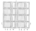
- FIG. 5 is a top perspective view of the intermediate product in a state where the large array substrate and the counter substrate are bonded together.
- FIG. 6 is a cross-sectional view taken along line AA in FIG. FIG. 5 shows a configuration when the counter substrate is seen through and the plane of the array substrate is seen from above.
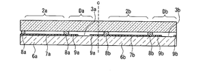
- a dotted line c indicates a cutting line (cutting line).
- resin films protective films 9a and 9b are provided in areas hatched with dots.
- each cell includes display areas 1a and 1b and terminal areas Da and Db.
- the protective films 9a and 9b are provided so as to cover the terminal portions Da and Db, and are formed to extend to a position straddling the dividing line c.
- the protective films 9a and 9b are patterned so that the external connection wiring (not shown) is exposed at a part of the terminal portions Da and Db. That is, in the terminal portions Da and Db, there are portions 3a and 3b that are not covered with the protective films 9a and 9b in a region that is not in contact with the periphery of the cell.
- the array substrates 6a and 6b and the counter substrates 5a and 5b are bonded together, they are divided into cells (S4 and S5).
- a scribe / break method can be used for the division.
- Each cell is provided with a protective resin (an example of an additional film) that covers the portions 3a and 3b that are not covered with the protective films 9a and 9b (that is, the portions where the external connection terminals are exposed) (S6).
- This protective resin is provided to protect the array substrates 6a and 6b and the external connection wiring from the etching solution in a later etching process.
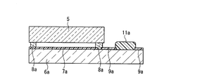
- FIG. 7 is a cross-sectional view of a single cell provided with a protective resin, that is, a liquid crystal display panel.
- the protective resin 11a is provided in a portion not covered with the protective film 9a.
- a jig for etching is further attached to the protective resin 11a.
- the protective film 9a and the array substrate 6a are formed on the same surface on the side surface on the dividing line c side in the divided cell. That is, the protective film 9a is formed up to the dividing edge on the surface of the array substrate 6a.
- the cell (liquid crystal display panel) thus formed is immersed in a glass etching solution (for example, 3 to 5% hydrofluoric acid solution) for 1 to 10 minutes, and the glass end face is etched (S7).
- a glass etching solution for example, 3 to 5% hydrofluoric acid solution
- FIG. 8B is a cross-sectional view taken along line AA of FIG. 8A.
- the jig connected to the protective resin 11 a is hung on the edge 14 a of the container containing the etching solution 13, so that the liquid crystal display panel is fixed in the etching solution 13.
- the liquid crystal display panel is taken out together with the jig, rinsed with pure water and dried with warm air to complete the etching. Thereafter, after attaching the polarizing plate, the protective resin 11a is removed (S8), and the FPC is connected to the exposed portion of the external connection wiring at the terminal portion Da (S9).
- a tape-shaped resin ACF bonder made of a conductive material is attached to the FPC and temporarily bonded at 80 ° C. The FPC is pressed against a portion where the external connection wiring of the liquid crystal display panel is exposed with a head heated to 200 ° C., and is finally bonded.
- the module is completed by processing such as IC mounting.
- a backlight device may be provided on the back surface of the liquid crystal panel. As a result, a liquid crystal display device including a liquid crystal panel and a backlight device is created.
- the protective film 9 is formed on the dividing line before the cell division, the cell substrate array substrate 6 can be covered with the protective film 9 up to the cell dividing edge. Therefore, the protective film 9 that protects the terminals can be formed on the array substrate 6 without excess or deficiency, and accurate etching of the sectional surface becomes possible. For example, in order to selectively etch the glass end face, it is necessary to apply a protective resin to a portion that is not etched, and it is difficult to spread this protective resin over the edges and the ridges on the substrate. The protective resin may sag on the etching surface (cross section of the substrate).
- the protective resin and the etching jig when fixed, the protective resin may hang down on the etching surface.
- etching of the portion where the protective resin hangs is hindered, so that micro cracks remain and the substrate becomes weak against bending stress.
- the etching proceeds in the portion where the protective resin is insufficiently applied, the tip of the substrate becomes thin and easily cracked.
- the protective film can be formed without excess or deficiency, occurrence of such a situation can be suppressed without particularly complicating the manufacturing process.
- FIG. 9 is a cross-sectional view of the liquid crystal display panel according to the second embodiment.
- the alignment film 7 is formed to extend to the terminal portion D and further to the edge of the array substrate 6. That is, the alignment film 7 also serves as the protective film 9 in the first embodiment.
- FIG. 10 is a flowchart showing an example of a processing flow in the manufacturing process of the liquid crystal display panel according to the present embodiment.
- the array substrate 6 on which a plurality of liquid crystal display panel patterns are formed and the counter substrate 5 on which a plurality of liquid crystal display panel black matrices or color filters are provided are bonded to each other and divided.
- a liquid crystal display panel is manufactured.
- the FPC is connected before etching.
- the polyimide resin alignment film 7 is printed on the glass substrate, respectively.
- the printing pattern of the alignment film 7 is usually printed only in a portion corresponding to the display area, and is not printed outside the display area.
- the alignment film is usually not provided because the alignment is unnecessary.
- the printing pattern of the alignment film 7 is formed so as to further extend from the display area and straddle the dividing line.
- the array substrates 6a and 6b and the counter substrates 5a and 5b thus provided with the alignment films 7a and 7b are bonded together by a seal printing process and a liquid crystal dropping process (S3).
- FIG. 11 is a top perspective view of the intermediate product in a state where the large array substrate and the counter substrate are bonded together.
- 12 is a cross-sectional view taken along the line AA in FIG.
- the alignment film 7 is provided in the area hatched with dots in FIG. That is, the alignment films 7a and 7b are provided so as to cover not only the display regions 1a and 1b but also the terminal portions Da and Db that are drawn out from the external connection wiring next to the display region and connected to the outside.
- the alignment films 7a and 7b are formed to extend to a position straddling the dividing line c between cells.
- the alignment films 7a and 7b are patterned so that the terminal portions Da and Db are not printed on the portions where the terminals are connected to the FPC. Thereby, the external connection wiring (not shown) is exposed in the portions 3a and 3b that are not covered with the alignment films 7a and 7b.
- the large format is divided into cells (S4, 5a).
- the dividing step first, in accordance with the outer shape of the cell, scribing by a wheel is vertically and horizontally inserted into the counter substrate. Next, the array substrate side is matched with the outer shape of the cell, and scribing with a wheel is performed.
- tolerances such as the play of the core of the wheel and the scribe line entering diagonally may occur, and the target line may be displaced.
- a tolerance is generated, a portion where polyimide is printed with an alignment film is divided. Therefore, the dividing edge in each cell after dividing is always in a state in which polyimide resin is coated.
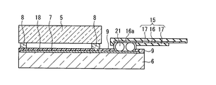
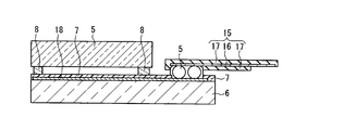
- the FPC is electrically connected to the portion of the cell (liquid crystal display panel) after the division where the alignment film 7 is removed from the terminal portion D through an ACF tape. Further, the FPC closes the portion where the alignment film 7 is removed, that is, the exposed surface of the array substrate (S6a). As described above, by attaching the FPC to the terminal connection portion of the cell (liquid crystal display panel) before the etching, the portion not to be etched can be covered. Therefore, a process such as forming a protective resin or the like becomes unnecessary. Further, even if the ACF bonder resin wraps around during the FPC connection, the ACF bonder resin is placed on the alignment film surface 9 formed on the array substrate. Only the cross section can be exposed.
- FIG. 13A is a view of the liquid crystal display panel being etched as viewed from the panel surface side
- FIG. 13B is a cross-sectional view taken along line AA of FIG. 13A.
- the clamp 19 sandwiching the FPC 15 is hooked on the edge 14 a of the container containing the etchant 13, so that the liquid crystal display panel is fixed in the etchant 13.
- the protective film (alignment film 7) for protecting the etching is formed at a position across the dividing line before dividing, so that the protective film can be formed up to the dividing edge. There is an effect that the protective film does not hang on the dividing surface. Furthermore, since the protective film is formed by patterning the alignment film 7, the manufacturing process is further simplified. In addition, by connecting an FPC, which is an example of a wiring covered with a polyimide resin, to the wiring connection terminal in advance, the liquid crystal display panel can be fixed and etched by the FPC.
- the present invention can be applied to a display panel used for a curved display.
- a display panel used for a curved display In a curved display using a glass substrate, it is necessary to reduce the glass thickness.
- a technique for this purpose there is a technique for thinning the liquid crystal panel after bonding by etching. By applying the present invention to this etching process, the strength of the substrate can be increased.
- a display panel using a glass substrate has been described.
- the present invention can also be applied to a display panel using a resin substrate.
- the display panel of the present invention is not limited to this. Specifically, the case where a protective film is formed on two or all four sides of the substrate is not excluded.
- the number of FPCs connected to the substrate is not limited, and two or more FPCs may be connected to the substrate.
Landscapes
- Physics & Mathematics (AREA)
- Nonlinear Science (AREA)
- Engineering & Computer Science (AREA)
- Manufacturing & Machinery (AREA)
- Mathematical Physics (AREA)
- Chemical & Material Sciences (AREA)
- Crystallography & Structural Chemistry (AREA)
- General Physics & Mathematics (AREA)
- Optics & Photonics (AREA)
- Devices For Indicating Variable Information By Combining Individual Elements (AREA)
Abstract
表示パネルの基板の所望の面をむらなくエッチングすることを可能にする。表示パネルの製造方法は、基板材に、複数の表示パネルとなる領域それぞれに回路配線を形成する工程と、前記基板材および前記回路配線の少なくとも一部を覆う保護膜(9a、9b)を、前記各表示パネルを分断する際の基板材の切断線(c)を跨ぐように形成する工程と、前記保護膜(9a、9b)が形成された後に前記切断線(c)に沿って前記基板材を切断することによって各表示パネルを分断する工程と、分断された表示パネルの分断面をエッチングする工程とを含む。
Description
本願の開示は、例えば液晶表示パネル等のような基板を有する表示パネルと、その製造方法に関する。
基板を有する表示パネルの薄型化のために、基板にエッチングを施されることがある。このエッチングの際、エッチングしたくない箇所(例えば、TFT端子面等)にエッチング防止のレジスト膜として樹脂を塗布することが提案されている(例えば、特許文献1参照)。
基板のエッチングは、基板の強度確保のためにも用いることができる。例えば、液晶表示パネルの場合、TFT基板およびCF基板の膜面(TFTまたはCFが形成された面)以外の全ての面をエッチングすることで、基板の微小クラックを除去し、強度を確保することができる。このエッチングの際、例えば、基板の膜面はエッチングせず、側面を選択的にエッチングするには、膜面のエッチングしない部分に保護樹脂(エッチング防止樹脂)を塗る必要がある。
しかし、この保護樹脂を基板の膜面のエッジや庇部分(側面との境界部分)に、過不足なく、行き渡らせるのは難しい。膜面を越えて側面に保護樹脂がはみ出したり(ダレの発生)、保護樹脂が境界部分まで届かずに、膜面のエッジに近い部分が露出したりすることが少なくない。他にも、保護樹脂に、エッチングに用いる治具を固定する場合に、保護樹脂が基板側面にはみ出す(ダレる)ことが多い。
このように基板のエッチング面へ保護樹脂がはみ出すと、基板をエッチング処理時に樹脂がはみ出した部分(ダレの部分)がエッチングされない。そのため、基板に微小クラックが残り、曲げ応力に対して弱い基板になってしまう。逆に、基板のエッチングをしない面において、保護樹脂が行き渡っていない部分(不足部分)が存在すると、エッチング面から前記不足部分へエッチングが進み、基板の先端が薄くなり割れやすくなる。
ゆえに、本発明は、表示パネルの基板の所望の面をむらなくエッチングすることを可能にする表示パネルまたはその製造方法を提供することを目的とする。
上記目的を達成するために、本願開示の製造方法は、基板材に、複数の表示パネルとなる領域それぞれに回路配線を形成する工程と、前記基板材および前記回路配線の少なくとも一部を覆う保護膜を、前記各表示パネルを分断する際の基板材の切断線を跨ぐように形成する工程と、前記保護膜が形成された後に前記切断線に沿って前記基板材を切断することによって各表示パネルを分断する工程と、分断された表示パネルの分断面をエッチングする工程とを含む。
上記製造方法によれば、表示パネルが基板材上で占める矩形領域の少なくとも1辺に保護膜が形成された状態で表示パネルが分断される。これにより、分断後の表示パネルでは、基板のエッジ(すなわち分断面)まで保護膜が行き渡る。すなわち、分断面においては、保護膜の側面と基板側面とがおなじ面に形成される。そのため、エッチングしない面における保護膜の不足、あるいはエッチング面への保護膜のはみ出しが抑えられる。その結果、所望の面をむらなくエッチングすることができ、ひいては、基板の強度が確保される。
上記製造方法においては、複数の表示パネルとなる領域それぞれに形成される前記回路配線は、表示パネルの外部とを接続する外部接続配線を含み、前記保護膜は、前記外部接続配線が形成された領域を覆い、前記外部接続配線のうち、外部配線と接続される端子部分を露出させるように形成され、前記エッチングにおいては、露出した前記端子部分にさらに付加膜を設けた状態で前記表示パネルの分断面がエッチングされ、エッチング後に前記付加膜が除去される態様であってもよい。
これにより、分断面をエッチングする際に、分断面をむらなくエッチングすることができる。また、エッチング後に付加膜を除去することで、端子部分を露出させて、外部配線が接続可能な構成とすることができる。
上記製造方法においては、複数の表示パネルとなる領域それぞれに形成される前記回路配線は、表示パネルの外部とを接続する外部接続配線を含み、前記保護膜は、前記外部接続配線が形成された領域を覆い、前記外部接続配線のうち、外部配線と接続される端子部分を露出させるように形成され、前記エッチングにおいては、露出した前記端子部分に樹脂で覆われた配線を接続した状態で前記表示パネルの分断面がエッチングされる態様であってもよい。
これにより、保護膜で覆われない外部接続配線の端子部分に、樹脂で覆われた配線で接続するため、エッチングしない部分を覆うことができる。そのため、保護膜形成およびエッチング工程を効率よく行うことができる。
上記製造方法においては、前記保護膜は、前記表示パネルの表示領域を覆う配向膜が、各表示パネルが基板材で占める矩形領域の周縁の少なくとも1つの辺を跨ぐように設けられることで形成される態様であってもよい。
これにより、配向膜形成過程において保護膜が形成されるので、さらに効率よく保護膜を形成することができる。
本願開示の表示パネルは、基板と、前記基板上の表示領域に設けられた、画像を表示するための回路配線と、前記基板および前記回路配線の少なくとも一部を覆う保護膜とを有し、前記保護膜の側面と基板の側面とは同じ面に形成される。
上記構成により、表示パネルの少なくとも1つの側面は、基板の側面をむらなくエッチングすることができる。
上記表示パネルにおいて、前記回路配線は、表示パネルの外部とを接続する外部接続配線を含み、前記保護膜は、前記外部接続配線が形成された領域を覆い、前記外部接続配線のうち、外部配線と接続される端子部分を露出させるように形成され、露出した前記端子部分には、樹脂で覆われた配線が接続される態様であってもよい。
前記保護膜は、前記外部接続配線が形成された領域を覆い、前記基板の側面のうち少なくとも1つの側面と同じ面上に側面を有する配向膜とすることができる。
本発明によれば、表示パネルの基板の所望の面をむらなくエッチングすることが可能になる。
以下、本発明のより具体的な実施形態について、図面を参照しながら説明する。なお、以下の実施形態は、本発明にかかる表示パネルを液晶表示パネルとして実施する場合の構成例を示したものであるが、本発明にかかる表示パネルは液晶表示パネルに限定されず、マトリクス状に画素が配置された基板を用いる任意の表示パネル(例えば、EL表示装置、プラズマディスプレイ等)に適用可能である。また、本発明にかかる表示パネルは、曲面ディスプレイに利用することもできる。
また、以下で参照する各図は、説明の便宜上、本発明の実施形態の構成部材のうち、本発明を説明するために必要な主要部材のみを簡略化して示したものである。従って、本発明にかかる表示装置は、本明細書が参照する各図に示されていない任意の構成部材を備え得る。また、各図中の部材の寸法は、実際の構成部材の寸法および各部材の寸法比率等を忠実に表したものではない。
[第1の実施形態]
[表示パネルの構成]
図1は、本実施形態にかかる液晶表示パネルの平面図であり、図2は、図1に示す液晶表示パネルのA-A線断面図である。図1および図2に示す例では、液晶表示パネル1は、複数のアクティブ素子(図示せず)が形成されたアレイ基板6と、対向基板5と、両基板の間に挟み込まれた液晶層とを備えている。アレイ基板6は、透明なガラス基板上に、図示しない、ソーススイッチング素子であるTFT(Thin Film Transistor)、や画素電極などがマトリクス状に形成された基板である。また、アレイ基板6は、スイッチング素子に接続されるソース電極およびゲート電極ならびに、これらを外部に引き出すための外部接続配線18も備える。図1においては、外部接続配線18の一部を省略して示している。アレイ基板6および対向基板5の液晶層側の表面には、配向膜7が設けられる。配向膜7では、所定のラビング方向に沿ってラビング処理が施されており、液晶層に含まれた液晶分子(図示せず)を所定方向に配向している。
[表示パネルの構成]
図1は、本実施形態にかかる液晶表示パネルの平面図であり、図2は、図1に示す液晶表示パネルのA-A線断面図である。図1および図2に示す例では、液晶表示パネル1は、複数のアクティブ素子(図示せず)が形成されたアレイ基板6と、対向基板5と、両基板の間に挟み込まれた液晶層とを備えている。アレイ基板6は、透明なガラス基板上に、図示しない、ソーススイッチング素子であるTFT(Thin Film Transistor)、や画素電極などがマトリクス状に形成された基板である。また、アレイ基板6は、スイッチング素子に接続されるソース電極およびゲート電極ならびに、これらを外部に引き出すための外部接続配線18も備える。図1においては、外部接続配線18の一部を省略して示している。アレイ基板6および対向基板5の液晶層側の表面には、配向膜7が設けられる。配向膜7では、所定のラビング方向に沿ってラビング処理が施されており、液晶層に含まれた液晶分子(図示せず)を所定方向に配向している。
対向基板5は、透明なガラス基板上に、例えば、赤、緑、青の3色のフィルタ層が形成された基板である。図示しないが、対向基板5には、対向電極や配向膜が設けられる。アレイ基板6と対向基板5とは、シール8により接続されている。液晶層は、アレイ基板6、対向基板5、およびシール8により封入される。
アレイ基板6において、対向基板5と重ならない領域は、外部接続配線18を外部へ接続するための端子が設けられる。以下では、この領域を端子部Dと称する。端子部Dは、アレイ基板6上に設けられた外部接続配線18とそれを覆う保護膜9が設けられる。図2に示すように、保護膜9の側面と基板6の側面とは同じ面に形成される。すなわち、アレイ基板6の端子部Dが配置される側は、エッジまで保護膜9で覆われている。なお、保護膜9で覆われていない辺では、配向膜がアレイ基板6をエッジまで覆っている。
端子部Dの一部は、保護膜9で覆われていない領域Eを有する。すなわち、保護膜9の一部が繰り抜かれている。この領域Eには、異方導電フィルム(ACF:Anisotropic Conductive Film)21を介してフレキシブル配線(FPC:flexible printed circuit)15が接続される。FPC15は、銅配線などの導電配線16と、導電配線16を覆う絶縁体層17を備える。具体的には、絶縁体層17として、ポリイミドフィルムなどを含む可撓性を有するベースフィルムが用いられる。導電配線16は、このベースフィルムの両面に銅箔などを用いて形成され、この導電配線16を保護する絶縁性フィルムがさらに設けられる。また、FPC15には、絶縁性フィルムの一部を除去し、導電配線16が露出された端子部16aが形成されている。そして、FPC15の端子部16aと、アレイ基板6の端子部Dに形成された領域Eとが、例えば、ACF21などの接続部材によって電気的に接続されている。これにより、FPC15は、アレイ基板6の端子部Dに引き出された外部接続配線18と接続される。
FPC15上には、例えば、電源回路や制御回路などの電子部品(図示せず)が実装されてもよい。FPC15は、外部接続配線18と接続されるため、FPC15に実装された電子部品から、アレイ基板6の画素回路に、外部接続配線18を通じて、制御信号や電源電圧などを供給することができる。なお、アレイ基板6上にも、スイッチング素子を駆動するためのドライバ回路が、例えば、COG(Chipon glass)方式で形成されてもよい。
[製造方法]
次に、本実施形態にかかる液晶表示パネルの製造方法について説明する。図3は、液晶表示パネルの製造工程における処理の流れの一例を示すフロー図である。図3に示す例では、まず、アレイ基板が作成される(S1)。図4は、アレイ基板の作成工程の一例を示すフロー図である。図4に示す例では、まず、基板材の一例であるマザーガラス上において複数の液晶表示パネルとなる領域それぞれに、ゲート電極、スイッチング回路およびソース電極を形成する(S11~S13)。例えば、ゲート電極は、画素の行方向に配置された複数のゲート線を含み、ソース電極は、列方向に配置された複数のソース線を含む。ゲート線とソース線の交点近傍に、スイッチング素子(例えば、TFT(Thin Film Transistor))が設けられる。すなわち、スイッチング素子はマトリクス状に形成される。また、ゲート電極およびソース電極をまとめて外部へ引き出すための外部接続配線が形成される。例えば、ゲート電極およびソース電極は、外部接続配線により、表示領域の隣の領域(図1に示す領域D)に引き出され、当該領域に外部と接続するための端子部が形成される。
次に、本実施形態にかかる液晶表示パネルの製造方法について説明する。図3は、液晶表示パネルの製造工程における処理の流れの一例を示すフロー図である。図3に示す例では、まず、アレイ基板が作成される(S1)。図4は、アレイ基板の作成工程の一例を示すフロー図である。図4に示す例では、まず、基板材の一例であるマザーガラス上において複数の液晶表示パネルとなる領域それぞれに、ゲート電極、スイッチング回路およびソース電極を形成する(S11~S13)。例えば、ゲート電極は、画素の行方向に配置された複数のゲート線を含み、ソース電極は、列方向に配置された複数のソース線を含む。ゲート線とソース線の交点近傍に、スイッチング素子(例えば、TFT(Thin Film Transistor))が設けられる。すなわち、スイッチング素子はマトリクス状に形成される。また、ゲート電極およびソース電極をまとめて外部へ引き出すための外部接続配線が形成される。例えば、ゲート電極およびソース電極は、外部接続配線により、表示領域の隣の領域(図1に示す領域D)に引き出され、当該領域に外部と接続するための端子部が形成される。
次に、マザーガラス面を覆う樹脂膜が形成される(S14)。この樹脂膜は、図2に示す保護膜9となる。このように、セル(個々の液晶表示パネル)の分断境界(切断線)を跨ぐように樹脂膜を構成する。このように、各液晶表示パネルとなるセルへの分断前から、セルの分断境界を跨ぐように樹脂膜を設けることで、分断後のセルの分断エッジまで樹脂膜で覆うことができる。これにより、端子保護のための保護膜(樹脂膜)を正確に、過不足なく端子部Dに設けることができる。その結果、後述するように、分断面の正確なエッチングが可能になる。また、樹脂膜は、外部接続配線が引き出された端子部を覆うように設けられ、端子部の一部で外部接続配線が露出するようにパターニングされる。樹脂膜には、例えば、感光性アクリル樹脂等の感光性樹脂材料を用いることができる。樹脂膜形成工程においては、フォトリソグラフィにより感光性アクリル樹脂のパターンを形成することができる。樹脂膜が形成されると、画素電極として、例えばITOをスパッタリングにより、パターニングする(S15)。その後、表示領域を含む領域に配向膜が形成される。
この樹脂膜は、具体的には、アレイ基板および対向基板の表面の段差を緩和する感光性アクリル樹脂によるオーバーコート膜とすることができる。オーバーコート膜のパターン形成は、例えば、基板状態で完成した両基板に樹脂をスロットやスピン塗布を行い、露光にて先ほどと同様に端子の部分だけパターン抜きすることで実現できる。
図3を再び参照し、アレイ基板作成後、対向基板が作成される。透明なマザーガラス上に、カラーフィルタ、ブラックマトリクス、対向電極等、配向膜等が形成される。カラーフィルタとしては、例えば、複数の液晶表示パネルの表示領域ごと、赤、緑、青の3色のフィルタ層が形成される。
マザーガラスを含む大判のアレイ基板と、大判の対向基板は、シールを介して貼り合せられる(S3)。図5は、大判のアレイ基板と対向基板が貼り合わせられた状態における中間製品の上面透視図である。図6は、図5のA-A線における断面図である。図5においては、対向基板を透視してアレイ基板の平面を上から見た場合の構成を示している。また、点線cは、切断線(分断ライン)を示している。図5においてドットでハッチングした領域に樹脂膜(保護膜9a、9b)が設けられる。
図5および図6に示す例では、各セルは、表示領域1a、1bおよび端子領域Da、Dbを含む。保護膜9a、9bは、端子部Da、Dbを覆うように設けられ、分断ラインcを跨ぐ位置まで延びて形成される。また、保護膜9a、9bは、外部接続配線(図示せず)が、端子部Da、Dbの一部で露出するようにパターニングされる。すなわち、端子部Da、Dbにおいて、セルの周縁と接しない領域において、保護膜9a、9bに覆われない部分3a、3bが存在している。
このように、アレイ基板6a、6bと対向基板5a、5bを貼り合わせた後、各セルに分断する(S4、S5)。分断には、例えば、スクライブ・ブレーク法を用いることができる。
各セルには、保護膜9a、9bで覆われていない部分3a、3b(すなわち、外部接続端子が露出した部分)を覆う保護樹脂(付加膜の一例)を設けられる(S6)。この保護樹脂は、後のエッチング工程で、エッチング液からアレイ基板6a、6bおよび外部接続配線を保護するために設けられるものである。図7は、保護樹脂が設けられた単セル、すなわち、液晶表示パネルの断面図である。図7に示す例では、保護膜9aで覆われていない部分に保護樹脂11aが設けられる。保護樹脂11aには、さらにエッチングのための冶具が取り付けられる。
なお、図7に示すように、分断後のセルにおける分断線c側の側面では、保護膜9aとアレイ基板6aとが同じ面上に形成されている。すなわち、アレイ基板6aの表面においては分断エッジまで保護膜9aが形成される。
こうしてできたセル(液晶表示パネル)を、1分~10分の間ガラスエッチング液(例えば、3~5%フッ酸溶液)に浸漬し、ガラス端面をエッチングする(S7)。図8Aは、エッチングしている液晶表示パネルをパネル面側から見た図であり、図8Bは、図8AのA-A線断面図である。図8A、図8Bに示す例では、保護樹脂11aに接続された冶具が、エッチング液13の入った容器の縁14aに掛けられることにより、液晶表示パネルがエッチング液13内に固定される。これにより、対向基板5aのアレイ基板6aと対向する面の反対側の面および側面と、アレイ基板6aの対向基板5aと対向する面の反対側の面および側面がエッチング液にさらされた状態となる。そのため、対向基板5aとアレイ基板6aでガラスが露出している面は全てエッチングすることができる。
一定時間のエッチング後、冶具ごと液晶表示パネルを取り出し、純水によるリンス、温風乾燥しエッチングが完了する。この後、偏光板を貼り付けた後、保護樹脂11aを除去し(S8)、端子部Daで外部接続配線の露出した部分に、FPCを接続する(S9)。例えば、FPCに、導電性素材のテープ状の樹脂ACFボンダーを貼り付け80℃で仮圧着する。このFPCを液晶表示パネルの外部接続配線が露出した部分に対して、200度に過熱したヘッドで押し付け、本圧着する。FPC圧着後、ICの実装などの処理により、モジュールが完成する。なお、液晶パネルの背面にバックライト装置を設けてもよい。これにより、液晶パネルおよびバックライト装置を備えた液晶表示装置が作成される。
[効果、その他]
本実施形態によれば、セル分断前に、分断線上に保護膜9を構成するので、セル分断のアレイ基板6を、セルの分断エッジまで保護膜9で覆うことができる。そのため、端子を保護する保護膜9を、アレイ基板上6に過不足なく形成することができ、分断面の正確なエッチングが可能になる。例えば、ガラス端面を選択的にエッチングするには、エッチングしない部分に保護樹脂を塗る必要があり、この保護樹脂を基板上のエッジや庇部分にいきわたらせるのは難しい。保護樹脂がエッチング面(基板分断面)に垂れることもある。他にも、保護樹脂とエッチング治具を固定する場合に保護樹脂がエッチング面に垂れることもある。このような場合、ガラス基板エッチングの際、保護樹脂が垂れた部分のエッチングが妨げられるために、微小クラックが残り、曲げ応力に対して弱い基板になってしまう。逆に、保護樹脂の塗布不足部分ではエッチングが進むため、基板の先端が薄くなり割れやすくなる。本実施形態によれば、上記のとおり、保護膜を過不足なく形成することができるので、特に製造工程を複雑にしなくても、このような事態の発生を抑えることができる。
本実施形態によれば、セル分断前に、分断線上に保護膜9を構成するので、セル分断のアレイ基板6を、セルの分断エッジまで保護膜9で覆うことができる。そのため、端子を保護する保護膜9を、アレイ基板上6に過不足なく形成することができ、分断面の正確なエッチングが可能になる。例えば、ガラス端面を選択的にエッチングするには、エッチングしない部分に保護樹脂を塗る必要があり、この保護樹脂を基板上のエッジや庇部分にいきわたらせるのは難しい。保護樹脂がエッチング面(基板分断面)に垂れることもある。他にも、保護樹脂とエッチング治具を固定する場合に保護樹脂がエッチング面に垂れることもある。このような場合、ガラス基板エッチングの際、保護樹脂が垂れた部分のエッチングが妨げられるために、微小クラックが残り、曲げ応力に対して弱い基板になってしまう。逆に、保護樹脂の塗布不足部分ではエッチングが進むため、基板の先端が薄くなり割れやすくなる。本実施形態によれば、上記のとおり、保護膜を過不足なく形成することができるので、特に製造工程を複雑にしなくても、このような事態の発生を抑えることができる。
[第2の実施形態]
図9は、第2の実施形態にかかる液晶表示パネルの断面図である。図9において、図2に示す液晶表示パネルと同じ部材には同じ符号を付している。図9に示す液晶表示パネルでは、配向膜7が、端子部Dまでのび、さらに、アレイ基板6のエッジまで延びて形成されている。すなわち、配向膜7は、上記第1の実施形態における保護膜9の役割も果たしている。
図9は、第2の実施形態にかかる液晶表示パネルの断面図である。図9において、図2に示す液晶表示パネルと同じ部材には同じ符号を付している。図9に示す液晶表示パネルでは、配向膜7が、端子部Dまでのび、さらに、アレイ基板6のエッジまで延びて形成されている。すなわち、配向膜7は、上記第1の実施形態における保護膜9の役割も果たしている。
図10は、本実施形態にかかる液晶表示パネルの製造工程における処理の流れの一例を示すフロー図である。図10に示す例は、複数の液晶表示パネル用のパターンが形成されたアレイ基板6と、複数の液晶表示パネル用ブラックマトリックス若しくはカラーフィルタが設けられた対向基板5を貼り合せて、分断することで液晶表示パネルが作製される。この製造工程においては、エッチング前にFPCが接続される。
アレイ基板の作成(SS1)と対向基板の作成(S2)においては、それぞれ、ガラス基板にポリイミド樹脂の配向膜7を印刷する。このとき、配向膜7の印刷パターンは、従来では、表示領域に相当する部分のみ印刷され、表示領域以外には印刷しないのが普通であった。特に、回路配線を外部へ接続する端子がある部分では、配向が不要なため配向膜が設けられないのが普通であった。これに対して、本実施形態では、配向膜7の印刷パターンは、表示領域からさらに延びて、分断線を跨ぐように形成される。
配向膜7a、7bのパターニング後、ラビングが行われる。このように配向膜7a、7bが施されたアレイ基板6a、6bおよび対向基板5a、5bは、シール印刷処理、液晶滴下処理により、貼り合せられる(S3)。
図11は、大判のアレイ基板と対向基板が貼り合わせられた状態における中間製品の上面透視図である。図12は、図11のA-A線における断面図である。本実施形態では、図11においてドットでハッチングした領域に配向膜7が設けられる。すなわち、配向膜7a、7bは、表示領域1a、1bだけでなく、表示領域の隣の外部接続配線が引き出され外部へ接続される端子部Da、Dbも覆うように設けられる。配向膜7a、7bは、さらに、セル間の分断ラインcを跨ぐ位置まで延びて形成される。また、配向膜7a、7bは、端子部Da、Dbにおいて、端子がFPCに接続される部分には印刷されないようにパターニングされる。これにより、配向膜7a、7bに覆われない部分3a、3bでは、外部接続配線(図示せず)が露出する。
次に、大判をセル単位に分断する(S4、5a)。分断工程では、まず、セルの外形に合わせて、対向基板に対して、ホイールによるスクライブを縦横に入れていく。次にアレイ基板側をセル外形に合わせて、ホイールによるスクライブを入れる。スクライブを入れる時に、ホイールの芯の遊びやスクライブラインが斜めに入るなどの公差が発生し、狙ったラインにずれが生じることもある。しかし、本実施形態では、公差が発生したとしても、ポリイミドが配向膜印刷されている部分を分断することになる。そのため、分断後の各セルにおける分断エッジには必ずポリイミド樹脂がコーティングされた状態になる。
分断後のセル(液晶表示パネル)の、端子部Dにおける配向膜7が抜かれた部分には、ACFテープを介してFPCが電気的に接続される。また、このFPCによって、配向膜7が抜かれた部分、すなわち、露出していたアレイ基板の表面が塞がれる(S6a)。このように、エッチング前に、セル(液晶表示パネル)の端子接続部分にFPCを取り付けておくことで、エッチングしない部分を、覆うことができる。そのため、別途保護樹脂等を形成するなどの工程が不要になる。また、FPC接続の際にACFボンダー樹脂の回りこみがあったとしても、アレイ基板上に構成した配向膜面9上にACFボンダー樹脂がのるので、分断後のガラス端面を覆うことなく、分断面のみをむき出しにすることができる。
次に、液晶表示パネルをFPC15とクランプで固定した状態で、1分~10分の間、ガラスエッチング液(例えば、3~5%フッ酸溶液)にFPC15の部分まで浸漬し、ガラス端面をエッチングする(S7)。これにより、分断による傷を、ガラスエッチングにより取り除くことができる。図13Aは、エッチングしている液晶表示パネルをパネル面側から見た図であり、図13Bは、図13AのA-A線断面図である。図13A、図13Bに示す例では、FPC15を挟むクランプ19が、エッチング液13の入った容器の縁14aに掛けられることにより、液晶表示パネルがエッチング液13内に固定される。この状態で液晶パネルをエッチングすることで、ガラスの膜面以外の全ての面をエッチングすることができる。
本実施形態によれば、第1の実施形態と同様に、エッチング保護する保護膜(配向膜7)が、分断前に分断線を跨ぐ位置に形成されるので、分断エッジまで保護膜が形成できる、分断面への保護膜が垂れないといった効果を奏する。さらに、配向膜7のパターニングで保護膜を形成するので、製造工程がさらに簡単になる。また、配線接続端子にポリイミド樹脂で覆われた配線の一例であるFPCをあらかじめ接続することで、液晶表示パネルをFPCで固定してエッチングすることができる。
以上、実施形態について説明したが、本発明は、上記実施形態に限られない。例えば、曲面ディスプレイに用いられる表示パネルにも本発明を適用することができる。ガラス基板を用いた曲面ディスプレイでは、ガラス厚を薄くする必要がある。このための手法として、貼り合せ後の液晶パネルをエッチング処理により薄型化する手法がある。このエッチング処理に、本発明を適用することで、基板の強度を上げることができる。
また、上記実施形態では、ガラス基板を用いた表示パネルについて説明したが、樹脂基板を用いた表示パネルについても本発明を同様に適用することができる。
また、図1では、基板の周辺部の1辺に保護膜を設ける例を示したが、本発明の表示パネルはこれに限られるものではない。具体的には、基板の2辺、もしくは4辺全てに保護膜が形成される場合を排除するものではない。また、基板に接続されるFPCの枚数にも制限はなく、2枚以上のFPCが基板に接続される場合もある。
1 液晶表示パネル
2 表示領域
5 対向基板
6 アレイ基板
7 配向膜
8 シール
9 保護膜
11a 保護樹脂
16 導電配線
17 絶縁体層
18 外部接続配線
2 表示領域
5 対向基板
6 アレイ基板
7 配向膜
8 シール
9 保護膜
11a 保護樹脂
16 導電配線
17 絶縁体層
18 外部接続配線
Claims (7)
- 基板材に、複数の表示パネルとなる領域それぞれに回路配線を形成する工程と、
前記基板材および前記回路配線の少なくとも一部を覆う保護膜を、前記各表示パネルを分断する際の基板材の切断線を跨ぐように形成する工程と、
前記保護膜が形成された後に前記切断線に沿って前記基板材を切断することによって各表示パネルを分断する工程と、
分断された表示パネルの分断面をエッチングする工程とを含む、表示パネルの製造方法。 - 複数の表示パネルとなる領域それぞれに形成される前記回路配線は、表示パネルの外部とを接続する外部接続配線を含み、
前記保護膜は、前記外部接続配線が形成された領域を覆い、前記外部接続配線のうち、外部配線と接続される端子部分を露出させるように形成され、
前記エッチングにおいては、露出した前記端子部分にさらに付加膜を設けた状態で前記表示パネルの分断面がエッチングされ、エッチング後に前記付加膜が除去される、請求項1に記載の表示パネルの製造方法。 - 複数の表示パネルとなる領域それぞれに形成される前記回路配線は、表示パネルの外部とを接続する外部接続配線を含み、
前記保護膜は、前記外部接続配線が形成された領域を覆い、前記外部接続配線のうち、外部配線と接続される端子部分を露出させるように形成され、
前記エッチングにおいては、露出した前記端子部分に樹脂で覆われた配線を接続した状態で前記表示パネルの分断面がエッチングされる、請求項1に記載の製造方法。 - 前記保護膜は、前記表示パネルの表示領域を覆う配向膜が、各表示パネルが基板材で占める矩形領域の周縁の少なくとも1つの辺を跨ぐように設けられることで形成される、請求項1から3のいずれか1項記載の製造方法。
- 基板と、
前記基板上の表示領域に設けられた、画像を表示するための回路配線と、
前記基板および前記回路配線の少なくとも一部を覆う保護膜とを有し、
前記保護膜の側面と基板の側面とは同じ面に形成される、表示パネル。 - 前記回路配線は、表示パネルの外部とを接続する外部接続配線を含み、
前記保護膜は、前記外部接続配線が形成された領域を覆い、前記外部接続配線のうち、外部配線と接続される端子部分を露出させるように形成され、
露出した前記端子部分には、樹脂で覆われた配線が接続される、請求項5に記載の表示パネル。 - 前記保護膜は、前記外部接続配線が形成された領域を覆い、前記基板の側面のうち少なくとも1つの側面と同じ面上に側面を有する配向膜である、請求項5または6に記載の表示パネル。
Priority Applications (1)
| Application Number | Priority Date | Filing Date | Title |
|---|---|---|---|
| US13/375,710 US20120069509A1 (en) | 2009-06-12 | 2010-05-28 | Method for fabricating display panel |
Applications Claiming Priority (2)
| Application Number | Priority Date | Filing Date | Title |
|---|---|---|---|
| JP2009-141473 | 2009-06-12 | ||
| JP2009141473 | 2009-06-12 |
Publications (1)
| Publication Number | Publication Date |
|---|---|
| WO2010143543A1 true WO2010143543A1 (ja) | 2010-12-16 |
Family
ID=43308798
Family Applications (1)
| Application Number | Title | Priority Date | Filing Date |
|---|---|---|---|
| PCT/JP2010/059099 Ceased WO2010143543A1 (ja) | 2009-06-12 | 2010-05-28 | 表示パネルの製造方法 |
Country Status (2)
| Country | Link |
|---|---|
| US (1) | US20120069509A1 (ja) |
| WO (1) | WO2010143543A1 (ja) |
Cited By (2)
| Publication number | Priority date | Publication date | Assignee | Title |
|---|---|---|---|---|
| JP2017503745A (ja) * | 2014-01-10 | 2017-02-02 | コーニング インコーポレイテッド | ガラス基板のエッジを強化する方法 |
| JP2020038265A (ja) * | 2018-09-03 | 2020-03-12 | 凸版印刷株式会社 | 調光ユニット、および、調光板 |
Families Citing this family (5)
| Publication number | Priority date | Publication date | Assignee | Title |
|---|---|---|---|---|
| TWI485846B (zh) * | 2011-11-16 | 2015-05-21 | 友達光電股份有限公司 | 具可撓性基板之顯示裝置及其製造方法 |
| JP6263337B2 (ja) * | 2013-05-31 | 2018-01-17 | 株式会社ジャパンディスプレイ | 表示装置及びその製造方法 |
| CN104280958B (zh) * | 2014-09-26 | 2017-03-08 | 京东方科技集团股份有限公司 | 一种阵列基板及其制作方法、显示装置 |
| CN105810098A (zh) * | 2016-05-06 | 2016-07-27 | 京东方科技集团股份有限公司 | 显示母板和显示基板的制备方法、显示面板及显示装置 |
| CN113651539A (zh) * | 2021-08-16 | 2021-11-16 | 江西沃格光电股份有限公司 | 玻璃基板的减薄方法 |
Citations (4)
| Publication number | Priority date | Publication date | Assignee | Title |
|---|---|---|---|---|
| JP2001075117A (ja) * | 1999-09-06 | 2001-03-23 | Seiko Epson Corp | 液晶装置の製造方法 |
| JP2003315774A (ja) * | 2002-04-18 | 2003-11-06 | Seiko Epson Corp | 電気光学パネル、電子機器及び電気光学パネルの製造方法 |
| JP2004191573A (ja) * | 2002-12-10 | 2004-07-08 | Seiko Epson Corp | 電気光学装置の製造方法、電気光学装置、および電子機器 |
| JP2008009356A (ja) * | 2006-05-31 | 2008-01-17 | Optrex Corp | 表示パネルの製造方法およびパネル体の製造方法 |
Family Cites Families (2)
| Publication number | Priority date | Publication date | Assignee | Title |
|---|---|---|---|---|
| TWI238444B (en) * | 2002-12-10 | 2005-08-21 | Seiko Epson Corp | Method for manufacturing optoelectronic device, optoelectronic device and electronic machine |
| JP4916666B2 (ja) * | 2005-01-12 | 2012-04-18 | 株式会社 日立ディスプレイズ | 表示装置 |
-
2010
- 2010-05-28 US US13/375,710 patent/US20120069509A1/en not_active Abandoned
- 2010-05-28 WO PCT/JP2010/059099 patent/WO2010143543A1/ja not_active Ceased
Patent Citations (4)
| Publication number | Priority date | Publication date | Assignee | Title |
|---|---|---|---|---|
| JP2001075117A (ja) * | 1999-09-06 | 2001-03-23 | Seiko Epson Corp | 液晶装置の製造方法 |
| JP2003315774A (ja) * | 2002-04-18 | 2003-11-06 | Seiko Epson Corp | 電気光学パネル、電子機器及び電気光学パネルの製造方法 |
| JP2004191573A (ja) * | 2002-12-10 | 2004-07-08 | Seiko Epson Corp | 電気光学装置の製造方法、電気光学装置、および電子機器 |
| JP2008009356A (ja) * | 2006-05-31 | 2008-01-17 | Optrex Corp | 表示パネルの製造方法およびパネル体の製造方法 |
Cited By (2)
| Publication number | Priority date | Publication date | Assignee | Title |
|---|---|---|---|---|
| JP2017503745A (ja) * | 2014-01-10 | 2017-02-02 | コーニング インコーポレイテッド | ガラス基板のエッジを強化する方法 |
| JP2020038265A (ja) * | 2018-09-03 | 2020-03-12 | 凸版印刷株式会社 | 調光ユニット、および、調光板 |
Also Published As
| Publication number | Publication date |
|---|---|
| US20120069509A1 (en) | 2012-03-22 |
Similar Documents
| Publication | Publication Date | Title |
|---|---|---|
| KR101182521B1 (ko) | 액정 표시 장치 및 이의 제조 방법 | |
| US8547505B2 (en) | Liquid crystal display | |
| KR101812051B1 (ko) | 표시 장치 및 이의 제조 방법 | |
| WO2010143543A1 (ja) | 表示パネルの製造方法 | |
| US9437616B2 (en) | Display apparatus | |
| US20100182530A1 (en) | Display cell | |
| CN101093331A (zh) | 面板基板、显示装置及其制造方法 | |
| JP2000039622A (ja) | パッド部を有する平版表示装置及びその製造方法 | |
| KR20110067261A (ko) | 액정표시장치 및 그의 제조방법 | |
| JP6862380B2 (ja) | 表示装置及び表示装置の製造方法 | |
| JP2009031362A (ja) | 配線基板、その製造方法、及び表示装置 | |
| US20210405478A1 (en) | Array substrate and manufacturing method thereof, and display panel | |
| CN100582897C (zh) | 液晶面板制造方法 | |
| KR101644055B1 (ko) | 외곽영역이 최소화된 액정표시장치 | |
| KR101616927B1 (ko) | 액정표시장치 제조 방법 | |
| CN1983607A (zh) | 显示装置及其制造方法 | |
| WO2011024556A1 (ja) | 液晶モジュールの静電気除去方法、液晶表示装置の製造方法、及び液晶モジュール | |
| WO2012057027A1 (ja) | タッチパネル、表示装置およびタッチパネルの製造方法 | |
| US20120325536A1 (en) | Display device and method for fabricating same | |
| JP2008203448A (ja) | 液晶表示装置 | |
| KR101153299B1 (ko) | 액정표시소자 및 그 제조방법 | |
| KR100957614B1 (ko) | 액정표시장치용 어레이 기판 및 그 제조 방법 | |
| KR101226594B1 (ko) | 어레이 기판의 제조방법 및 이를 이용한 표시패널의제조방법 | |
| JP2010139962A (ja) | アレイ基板、平面表示装置、マザー基板及びアレイ基板の製造方法 | |
| JP2008216966A (ja) | 電気光学装置の製造方法、電気光学装置及び電子機器 |
Legal Events
| Date | Code | Title | Description |
|---|---|---|---|
| 121 | Ep: the epo has been informed by wipo that ep was designated in this application |
Ref document number: 10786074 Country of ref document: EP Kind code of ref document: A1 |
|
| WWE | Wipo information: entry into national phase |
Ref document number: 13375710 Country of ref document: US |
|
| NENP | Non-entry into the national phase |
Ref country code: DE |
|
| 122 | Ep: pct application non-entry in european phase |
Ref document number: 10786074 Country of ref document: EP Kind code of ref document: A1 |
|
| NENP | Non-entry into the national phase |
Ref country code: JP |