WO2010140545A1 - 湿度検出センサパッケージ及びその製造方法 - Google Patents
湿度検出センサパッケージ及びその製造方法 Download PDFInfo
- Publication number
- WO2010140545A1 WO2010140545A1 PCT/JP2010/059086 JP2010059086W WO2010140545A1 WO 2010140545 A1 WO2010140545 A1 WO 2010140545A1 JP 2010059086 W JP2010059086 W JP 2010059086W WO 2010140545 A1 WO2010140545 A1 WO 2010140545A1
- Authority
- WO
- WIPO (PCT)
- Prior art keywords
- humidity detection
- detection sensor
- partition member
- base
- sensor package
- Prior art date
- Legal status (The legal status is an assumption and is not a legal conclusion. Google has not performed a legal analysis and makes no representation as to the accuracy of the status listed.)
- Ceased
Links
Images


Classifications
-
- G—PHYSICS
- G01—MEASURING; TESTING
- G01N—INVESTIGATING OR ANALYSING MATERIALS BY DETERMINING THEIR CHEMICAL OR PHYSICAL PROPERTIES
- G01N33/00—Investigating or analysing materials by specific methods not covered by groups G01N1/00 - G01N31/00
- G01N33/0004—Gaseous mixtures, e.g. polluted air
- G01N33/0009—General constructional details of gas analysers, e.g. portable test equipment
-
- H—ELECTRICITY
- H10—SEMICONDUCTOR DEVICES; ELECTRIC SOLID-STATE DEVICES NOT OTHERWISE PROVIDED FOR
- H10W—GENERIC PACKAGES, INTERCONNECTIONS, CONNECTORS OR OTHER CONSTRUCTIONAL DETAILS OF DEVICES COVERED BY CLASS H10
- H10W72/00—Interconnections or connectors in packages
- H10W72/50—Bond wires
- H10W72/531—Shapes of wire connectors
- H10W72/536—Shapes of wire connectors the connected ends being ball-shaped
-
- H—ELECTRICITY
- H10—SEMICONDUCTOR DEVICES; ELECTRIC SOLID-STATE DEVICES NOT OTHERWISE PROVIDED FOR
- H10W—GENERIC PACKAGES, INTERCONNECTIONS, CONNECTORS OR OTHER CONSTRUCTIONAL DETAILS OF DEVICES COVERED BY CLASS H10
- H10W72/00—Interconnections or connectors in packages
- H10W72/50—Bond wires
- H10W72/531—Shapes of wire connectors
- H10W72/5363—Shapes of wire connectors the connected ends being wedge-shaped
-
- H—ELECTRICITY
- H10—SEMICONDUCTOR DEVICES; ELECTRIC SOLID-STATE DEVICES NOT OTHERWISE PROVIDED FOR
- H10W—GENERIC PACKAGES, INTERCONNECTIONS, CONNECTORS OR OTHER CONSTRUCTIONAL DETAILS OF DEVICES COVERED BY CLASS H10
- H10W72/00—Interconnections or connectors in packages
- H10W72/50—Bond wires
- H10W72/541—Dispositions of bond wires
- H10W72/5449—Dispositions of bond wires not being orthogonal to a side surface of the chip, e.g. fan-out arrangements
-
- H—ELECTRICITY
- H10—SEMICONDUCTOR DEVICES; ELECTRIC SOLID-STATE DEVICES NOT OTHERWISE PROVIDED FOR
- H10W—GENERIC PACKAGES, INTERCONNECTIONS, CONNECTORS OR OTHER CONSTRUCTIONAL DETAILS OF DEVICES COVERED BY CLASS H10
- H10W72/00—Interconnections or connectors in packages
- H10W72/851—Dispositions of multiple connectors or interconnections
- H10W72/874—On different surfaces
- H10W72/884—Die-attach connectors and bond wires
-
- H—ELECTRICITY
- H10—SEMICONDUCTOR DEVICES; ELECTRIC SOLID-STATE DEVICES NOT OTHERWISE PROVIDED FOR
- H10W—GENERIC PACKAGES, INTERCONNECTIONS, CONNECTORS OR OTHER CONSTRUCTIONAL DETAILS OF DEVICES COVERED BY CLASS H10
- H10W72/00—Interconnections or connectors in packages
- H10W72/90—Bond pads, in general
- H10W72/931—Shapes of bond pads
- H10W72/932—Plan-view shape, i.e. in top view
-
- H—ELECTRICITY
- H10—SEMICONDUCTOR DEVICES; ELECTRIC SOLID-STATE DEVICES NOT OTHERWISE PROVIDED FOR
- H10W—GENERIC PACKAGES, INTERCONNECTIONS, CONNECTORS OR OTHER CONSTRUCTIONAL DETAILS OF DEVICES COVERED BY CLASS H10
- H10W90/00—Package configurations
- H10W90/701—Package configurations characterised by the relative positions of pads or connectors relative to package parts
- H10W90/731—Package configurations characterised by the relative positions of pads or connectors relative to package parts of die-attach connectors
- H10W90/734—Package configurations characterised by the relative positions of pads or connectors relative to package parts of die-attach connectors between a chip and a stacked insulating package substrate, interposer or RDL
-
- H—ELECTRICITY
- H10—SEMICONDUCTOR DEVICES; ELECTRIC SOLID-STATE DEVICES NOT OTHERWISE PROVIDED FOR
- H10W—GENERIC PACKAGES, INTERCONNECTIONS, CONNECTORS OR OTHER CONSTRUCTIONAL DETAILS OF DEVICES COVERED BY CLASS H10
- H10W90/00—Package configurations
- H10W90/701—Package configurations characterised by the relative positions of pads or connectors relative to package parts
- H10W90/751—Package configurations characterised by the relative positions of pads or connectors relative to package parts of bond wires
- H10W90/753—Package configurations characterised by the relative positions of pads or connectors relative to package parts of bond wires between laterally-adjacent chips
-
- H—ELECTRICITY
- H10—SEMICONDUCTOR DEVICES; ELECTRIC SOLID-STATE DEVICES NOT OTHERWISE PROVIDED FOR
- H10W—GENERIC PACKAGES, INTERCONNECTIONS, CONNECTORS OR OTHER CONSTRUCTIONAL DETAILS OF DEVICES COVERED BY CLASS H10
- H10W90/00—Package configurations
- H10W90/701—Package configurations characterised by the relative positions of pads or connectors relative to package parts
- H10W90/751—Package configurations characterised by the relative positions of pads or connectors relative to package parts of bond wires
- H10W90/754—Package configurations characterised by the relative positions of pads or connectors relative to package parts of bond wires between a chip and a stacked insulating package substrate, interposer or RDL
Definitions
- the present invention relates to a humidity detection sensor package and a manufacturing method thereof.
- Humidity detection sensors used for humidity change measurement include a capacitance-type humidity detection sensor using a polymer moisture-sensitive film whose dielectric constant changes according to the amount of absorbed or released moisture as a dielectric.
- a capacitive humidity detection sensor includes a sensor unit including the polymer moisture-sensitive film and a pair of electrodes that are covered with the polymer moisture-sensitive film and detects capacitance thereof, and pads provided at the ends of the pair of electrodes. The part can be electrically connected to an external circuit by wire bonding. In such a capacitive humidity detection sensor, it is necessary to expose the polymer moisture-sensitive film of the sensor part to the atmosphere, and it is required to seal at least the wire bonding part which is an external connection part with a sealing resin.
- Patent Document 1 an electronic component package partially sealed with a sealing resin is disclosed in Patent Document 1.
- the sensor region that is not sealed is protected by the cap member.
- sealing resin is coat
- the present invention has been made in view of the above points, and provides a humidity detection sensor package capable of efficiently obtaining a humidity detection sensor package in which thermal distortion does not occur at any operating temperature and variation in temperature characteristics is small, and a method for manufacturing the same.
- the purpose is to provide.
- the humidity detection sensor package of the present invention is mounted on one main surface of the package substrate, has a humidity detection sensor having a moisture sensitive region, a sealing resin for sealing at least an external connection portion of the humidity detection sensor, A partition member that partitions the sealing region of the sealing resin and the moisture sensitive region so that the moisture sensitive region is exposed to the outside, and the humidity detection sensor is provided on a base and on the base A sensor element mounted thereon, wherein the base and the partition member are made of the same material.
- the base of the humidity detection sensor and the partition member of the humidity detection sensor package are made of the same material, thermal distortion does not occur at any operating temperature, and variations in temperature characteristics can be reduced. it can.
- the base and the partition member are made of silicon.
- the base and the partition member are joined by eutectic bonding.
- the base and the partition member are bonded with a photosensitive adhesive.
- the partition member has a thin film formed by deposition of a fluorine-based gas.
- the partition member has a protruding portion protruding from the sealing resin, and the protruding portion has an R portion in plan view.
- the concave portion is preferably formed by photolithography and etching.
- the method for manufacturing a humidity detection sensor package of the present invention includes a step of mounting a humidity detection sensor on one main surface of a package substrate, a step of sealing an external connection portion of the humidity detection sensor with at least a sealing resin,
- the humidity detection sensor includes a moisture sensitive region and a partition member that partitions the sealing region of the sealing resin and the moisture sensitive region so that the moisture sensitive region is exposed to the outside.
- the humidity detection sensor includes a step of forming a recess facing the moisture sensitive region on one main surface of a substrate made of the same material as the partition member, and a step of mounting the sensor element on the base.
- the partition member And kicking step a step of dividing into individual humidity detection sensor by dicing along the dicing line, characterized in that it is produced by.
- a humidity detection sensor can be manufactured with high mass productivity. For this reason, a humidity detection sensor package can be manufactured efficiently.
- a humidity detection sensor package of the present invention it is preferable that only the base is diced along a dicing line to be divided into individual humidity detection sensors.
- the base and the partition member are divided into individual humidity detection sensors by dicing along a dicing line.
- the concave portion is formed by photolithography and etching.
- a thin film on the partition member by depositing a fluorine-based gas.
- the humidity detection sensor package of the present invention is mounted on one main surface of the package substrate, has a humidity detection sensor having a moisture sensitive region, a sealing resin for sealing at least an external connection portion of the humidity detection sensor, A partition member that partitions the sealing region of the sealing resin and the moisture sensitive region so that the moisture sensitive region is exposed to the outside, and the humidity detection sensor is provided on a base and on the base Since the base and the partition member are made of the same material, thermal distortion does not occur at any operating temperature, and variations in temperature characteristics can be reduced.
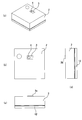
- FIG. 1 It is a figure which shows the humidity detection sensor package which concerns on embodiment of this invention, (a) is an isometric view, (b) is a top view, (c), (d) is a side view. .
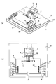
- (A)-(c) is a figure which shows the shape of the partition member and humidity detection hole in the humidity detection sensor package which concerns on embodiment of this invention.
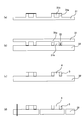
- (A)-(d) is a figure for demonstrating the manufacturing method of the humidity detection sensor package which concerns on embodiment of this invention.
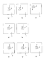
- (A)-(h) is a figure which shows the shape of the partition part of the humidity detection sensor package which concerns on embodiment of this invention, and the shape of a humidity detection hole.
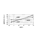
- (A)-(f) is a figure for demonstrating the manufacturing method of the humidity detection sensor package which concerns on embodiment of this invention. It is a figure which shows the relationship between the temperature and the change rate of a temperature characteristic in the humidity detection sensor package which concerns on embodiment of this invention.
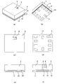
- FIG. 1 is a view showing a humidity detection sensor package according to an embodiment of the present invention, in which (a) is an isometric view, (b) is a bottom isometric view, and (c) is a plan view. It is a figure, (d) is a bottom view, (e) is a side view, (f) is sectional drawing.
- a humidity detection sensor 6 as an electronic component is mounted on one main surface of the package substrate 1, and the humidity detection is performed.
- the sensor 6 is sealed with the sealing resin 2.
- the humidity detection sensor 6 needs to expose the moisture sensitive area to the outside. For this reason, when the humidity detection sensor 6 is sealed with the sealing resin 2, the sealing region of the sealing resin 2 is separated from the moisture sensitive region in order to expose the humidity sensitive region of the humidity detection sensor 6 to the outside.
- the partition member 3 is provided in advance.
- the partition member 3 that partitions the sealing region of the sealing resin 2 from the moisture sensitive region is provided in advance, and the humidity detection sensor 6 is sealed with the sealing resin 2 to thereby reduce the humidity.
- the humidity detection sensor 6 can be sealed in a state where the humidity sensitive area of the detection sensor 6 is exposed to the outside (a state in which the humidity detection hole 4 is provided).
- the humidity detection sensor package is provided with a partition member 3 on a humidity detection sensor 6.
- the partition member 3 is joined to the humidity detection sensor 6 by a photosensitive adhesive (not shown) or the like.
- a photosensitive adhesive not shown
- the material of the base of the humidity detection sensor 6 and the material of the partition member 3 are the same, for example, in the case where the material of the base and the partition member 3 are made of silicon.
- the base and the partition member 3 may be joined by eutectic bonding.
- the package substrate 1 As the package substrate 1, a glass epoxy substrate or the like can be used. As shown in FIGS. 1A, 1 ⁇ / b> B, 1 ⁇ / b> E, and 1 ⁇ / b> F, the package substrate 1 includes a core material 12 and insulating layers 11 and 13 provided on both main surfaces of the core material 12. It is configured. Examples of the material constituting the insulating layers 11 and 13 include an insulating resist.
- the insulating layer (insulating layer on the surface opposite to the sensor mounting surface) 11 is provided with an opening for exposing the electrode portion 5 for mounting the humidity detection sensor package on a circuit board (not shown). Yes. By electrically connecting the electrode part 5 and the electrode part of the circuit board, the humidity detection sensor package can be mounted on the circuit board.
- the sealing resin 2 seals at least the external connection portion of the humidity detection sensor 6.
- an epoxy resin containing SiO 2 filler or the like can be used as the sealing resin 2. Sealing with the sealing resin 2 is performed by transfer molding, for example.
- the material of the partition member 3 is the same as the material of the base of the humidity detection sensor 6 to be described later, and examples thereof include silicon.
- the humidity detection sensor 6 of the humidity detection sensor package is a polymer film humidity sensor that uses a polymer moisture-sensitive material whose dielectric constant changes according to the amount of absorbed or released moisture as a dielectric.
- This humidity detection sensor 6 is die-bonded on the package substrate 1 with a die-bonding material 9.
- an IC 7 that controls the sensor element of the humidity detection sensor 6 is die-bonded by a die-bonding material 9.
- an opening for exposing the electrode pad 10 is provided in the insulating layer (insulating layer on the sensor mounting surface) 13 of the package substrate 1.
- the package substrate 1 and the humidity detection sensor 6 or the IC 7 can be electrically connected.
- the electrode pad 10 of the package substrate 1 and the electrode pad 14 of the humidity detection sensor 6 or IC 7 are electrically connected by a wire 8 which is an external connection part (wire bonding).
- the electrode pad 14 of the humidity detection sensor 6 and the electrode pad 14 of the IC 7 are also electrically connected by a wire 8 (wire bonding).
- the humidity detection sensor 6 is a capacitive humidity sensor.
- the capacitive humidity sensor includes a sensor element mounted on a base, and includes a sensing unit in which the capacitance Cs changes depending on humidity, and a reference unit that holds a constant capacitance Cr regardless of humidity.
- the sensing unit and the reference unit have a parallel plate structure including a lower electrode film, a polymer moisture sensitive film, and an upper electrode film.
- the lower electrode film, the polymer moisture sensitive film, and the upper electrode film are laminated on the base in order from the lower electrode film, and have substantially the same circular shape in plan view.
- the lower electrode film and the upper electrode film are made of, for example, an electrode material such as Al, and each film thickness is uniform.
- the polymer moisture sensitive film is made of polyimide or the like and is formed with a uniform film thickness.
- a non-moisture permeable protective film that blocks moisture exchange with the atmosphere is formed on the upper electrode film, and the entire upper electrode film is covered with the non-permeable protective film.
- the non-moisture permeable protective film is composed of, for example, a silicon nitride film (SiNx film) or an Al 2 O 3 / SiO 2 laminated film. Since the polymer moisture-sensitive film is covered with the upper electrode film and the moisture-impermeable protective film and is not exposed to the atmosphere, even if the humidity (moisture content) in the atmosphere changes, It does not change and the dielectric constant ⁇ does not change. Thereby, a certain electrostatic capacitance (reference capacitance) Cr is held between the lower electrode film and the upper electrode film.
- the moisture-impermeable protective film partially covers the upper electrode film. Since the polymer moisture-sensitive film is exposed to the atmosphere through a portion that is not covered with the moisture-impermeable protective film, the amount of moisture absorbed or released changes depending on the humidity (moisture amount) in the atmosphere, and the dielectric The rate ⁇ changes. As a result, the capacitance Cs between the lower electrode film and the upper electrode film changes.
- the IC 7 is electrically connected to the sensor element of the sensing unit and the sensor element of the reference unit, and the difference Cs ⁇ Cr between the capacitance Cs obtained by the sensing unit and the capacitance Cr obtained by the reference unit. Is converted to voltage and output.
- the partition member 3 is provided on the base of the humidity detection sensor 6.
- the partition member 3 has a humidity detection hole 4, and the sensor element of the sensing unit is exposed to the outside through the humidity detection hole 4. That is, the partition member 3 covers the sensor element of the reference part and exposes the sensor element (humidity sensitive area) of the sensing part. Thereby, while being able to expose the sensor element (humidity sensitive area
- the material constituting the base of the humidity detection sensor 6 and the material constituting the partition member 3 are the same. For this reason, since the same thermal expansion occurs in the base of the humidity detection sensor 6 and the partition member 3 at any operating temperature, no thermal distortion occurs. As a result, variation in temperature characteristics can be reduced.
- the base of the humidity detection sensor 6 and the partition member 3 are bonded to each other by a photosensitive adhesive or when the base material and the partition member 3 are made of silicon. For example, eutectic bonding via a sealing member such as a layer or direct bonding of Si—Si, for example, room temperature bonding.
- a partition member 3 having a humidity detection hole 4 as shown in FIGS. 3A and 3B may be provided.
- the humidity detection hole 4 is provided at a position shifted from the center of the partition member 3 in plan view, and has a circular shape.
- 3 (a) and 3 (b) the same parts as those in FIGS. 2 (a) and 2 (b) are denoted by the same reference numerals as those in FIGS. 2 (a) and 2 (b). Omitted.
- FIG. 4 is a diagram showing a humidity detection sensor package according to an embodiment of the present invention, where (a) is an isometric view, (b) is a plan view, and (c) and (d) are It is a side view.
- the partition member 3 protrudes from the surface of the sealing resin 2 as shown in FIGS.
- the partition member 3 has the R part 3b in planar view, as shown to Fig.5 (a), (b).
- FIG. 5B is an enlarged view of a portion X in FIG.
- the R portion 3b may be provided at a corner portion of the substantially rectangular partition member 3 in a plan view, and as shown in FIG. It may be provided over the entire outer shape of the partition member 3 in view.
- the outer shape of the partition member 3 in plan view may be substantially rectangular as shown in FIG. 5A, may be elliptical as shown in FIG. 5C, and is circular. May be.
- FIGS. 6A to 6D are views for explaining a method for manufacturing a humidity detection sensor package according to the embodiment of the present invention. In this method, only the base (substrate) is diced along a dicing line to be divided into individual humidity detection sensors.
- a portion 31a corresponding to the partition member and an opening 31b corresponding to the humidity detection hole are provided on the substrate 31 on the cap side by photolithography and etching (for example, deep RIE). .
- the side of the substrate 31 where the opening 31b is exposed is bonded to another substrate 32.
- the substrate 31 is bonded to another substrate 32 via the adhesive layer 33.
- the substrate 31 is ground to expose the opening 31b, and the humidity detection hole 4 is formed.
- another substrate 32 is fully diced into chips.
- the shape of the partition member 3 and the humidity detection hole 4 since the shape of the partition member 3 and the humidity detection hole 4 is determined by photolithography, the shape of the partition member 3 and the humidity detection hole 4 in a plan view can be changed to an arbitrary shape. Further, since the partition member 3 and the humidity detection hole 4 are formed by grinding instead of dicing, chipping can be suppressed to a low level, and particles generated by chipping can be prevented from affecting the moisture sensitive film. Further, since the humidity detection hole 4 is formed by grinding, no recess is formed in the vicinity of the bonding region between the substrates, and sludge accumulation during dicing and voids in the sealing resin can be prevented.
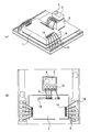
- FIGS. 7A to 7H are diagrams showing the shape of the partition portion and the shape of the humidity detection hole of the humidity detection sensor package according to the embodiment of the present invention.
- the position of the partition member 3 on the base may be the center of the base as shown in FIG. 7 (a), and deviated from the center of the base as shown in FIGS. 7 (b) and 7 (c). It may be a position (position close to either side).
- the shape of the partition member 3 in a plan view may be a rectangle as shown in FIGS. 7A to 7C, may be a circle as shown in FIG. It may be a polygonal shape (hexagonal shape in FIG. 7E) as shown in FIG.
- the shape of the humidity detection hole 4 in plan view may be circular as shown in FIGS. 7A to 7E, or may be rectangular as shown in FIG. 7 (g) may be a polygonal shape (an octagonal shape in FIG. 7 (g)), or may be an irregular shape as shown in FIG. 7 (h
- the humidity detection sensor 6 is formed with a recess facing the moisture sensitive region on one main surface of the substrate made of the same material as that of the partition member 3, and the sensor element is mounted on the base, and the recess is the moisture sensitive sensor. Dicing is performed by joining the substrate and the base so as to face the region, grinding the other main surface of the substrate to form an opening that exposes the moisture sensitive region to the outside, and providing the partition member. It is desirable to produce by dividing into individual humidity detection sensors by dicing along a line. According to this method, since the substrate and the base are joined in a multi-piece wafer state and then diced into chips, the humidity detection sensor 6 can be manufactured with high mass productivity. For this reason, a humidity detection sensor package can be manufactured efficiently.
- FIGS. 8 (a) to 8 (f) are diagrams for explaining a method of manufacturing a humidity detection sensor package according to the embodiment of the present invention.
- the base (substrate) and the partition member 3 are divided into individual humidity detection sensors by dicing along a dicing line.
- a resist layer 21 is formed on one main surface of the substrate 20 to be the partition member 3.
- the material constituting the substrate 20 is the same as the material constituting the base of the humidity detection sensor 6.
- a silicon substrate is used as the substrate 20.
- the resist layer 21 is patterned so that the opening 21a is formed in a region corresponding to a region that becomes a recess facing the moisture sensitive region.
- the substrate 20 is etched (for example, deep RIE) using the patterned resist layer 21 as a mask to form a recess 20a facing the moisture sensitive region in the substrate 20.
- the resist layer 21 is removed.
- sensor elements 61 and 62 are formed on the base 60 of the humidity detection sensor 6.
- the sensor element 61 is a sensor element of the sensing unit
- the sensor element 62 is a sensor element of the reference unit.
- These sensor elements 61 and 62 are formed by sequentially laminating a lower electrode film, a polymer moisture sensitive film, and an upper electrode film.
- the lower electrode film and the upper electrode film are formed by, for example, sputtering or the like, and then patterned, and the polymer moisture sensitive film is formed by applying polyimide in a predetermined pattern and drying.
- the photosensitive adhesive 22 is partially applied to a region other than the sensor elements 61 and 62 on the base 60.
- the material constituting the base 60 is silicon.
- the substrate 20 and the base 60 are bonded in a wafer state so that the concave portion 20a of the substrate 20 faces the moisture sensitive region (sensor element 61). At this time, the substrate 20 and the base 60 are joined by irradiating the photosensitive adhesive with light to cure.
- the other main surface of the substrate (the main surface opposite to the surface provided with the recesses) is ground to expose the moisture sensitive region (sensor element 61) to the outside. An opening (humidity detection hole 4) is formed and the partition member 3 is provided.
- the humidity detection sensor it is essential to expose the moisture-sensitive part to the atmosphere in the air. However, it is necessary to prevent the moisture-sensitive portion from getting into water and causing condensation. Therefore, it is preferable to form a fluorine-based thin film on the partition member 3 (particularly in the vicinity of the humidity detection hole 4). Thereby, the water applied to the humidity detection hole 4 can be made water repellent, and condensation in the moisture sensitive area can be prevented.
- a fluorine-based gas for example, CF 4 gas, C 4 F 8 gas, CHF 3 gas, or the like
- the thickness of the thin film is preferably about 10 nm.
- the water repellent treatment can be collectively performed in the wafer processing step, so that the inexpensive and uniform water repellent treatment can be applied to the partition member 3.
- the water that enters the humidity detection holes 4 can be made to repel water more effectively.
- the humidity detection sensor 6 manufactured in this way (the humidity detection sensor 6 manufactured by the method shown in FIG. 6 or FIG. 8) is die-bonded on the package substrate 1 with a die bond material 9.
- the IC 7 is also die-bonded on the package substrate 1 with a die-bonding material 9.
- the electrode pads 10 of the package substrate 1 and the electrode pads 14 of the humidity detection sensor 6 and the IC 7 are electrically connected by wire bonding. And it seals with the sealing resin 2 by transfer molding, and a humidity detection sensor package as shown in FIG. 1 is obtained.
- the package substrate 1 is diced along a dicing line to obtain a chip-like humidity detection sensor package.
- the base 60 of the humidity detection sensor 6 and the partition member 3 of the humidity detection sensor package are made of the same material, so that thermal distortion occurs at any operating temperature. Therefore, variation in temperature characteristics can be reduced.
- a humidity detection sensor package (Example 1) shown in FIG. 1 was produced by the above-described method using silicon as the material constituting the base and silicon as the material constituting the partition member.
- the material constituting the base is made of silicon and the material constituting the partition member is made of PPS (polyphenyl sulfide), and the humidity detection sensor package (Comparative Example 1) shown in FIG.
- the humidity detection sensor package (Comparative Example 2) shown in FIG. 1 was produced by the above-described method using silicon as the material constituting the base and gold as the material constituting the partition member.
- the variation in sensor output was suppressed to about 100 ppm, but in the humidity detection sensor package of Comparative Example 1, the variation in sensor output was about 400 ppm. In the humidity detection sensor package of Comparative Example 2, the sensor output variation was about 500 ppm.
- the reason why the variation in the sensor output of the humidity detection sensor package of Example 1 was small was considered to be that the materials constituting the base and the partition member were the same and there was no thermal distortion.
- the present invention is not limited to the above embodiment, and can be implemented with appropriate modifications.
- the material, the arrangement position of each layer, the thickness, the size, the manufacturing method, and the like in the above embodiment can be changed as appropriate.
- the present invention can be implemented with appropriate modifications without departing from the scope of the present invention.
Landscapes
- Chemical & Material Sciences (AREA)
- Life Sciences & Earth Sciences (AREA)
- Engineering & Computer Science (AREA)
- Health & Medical Sciences (AREA)
- Medicinal Chemistry (AREA)
- Food Science & Technology (AREA)
- Combustion & Propulsion (AREA)
- Physics & Mathematics (AREA)
- Analytical Chemistry (AREA)
- Biochemistry (AREA)
- General Health & Medical Sciences (AREA)
- General Physics & Mathematics (AREA)
- Immunology (AREA)
- Pathology (AREA)
- Investigating Or Analyzing Materials By The Use Of Electric Means (AREA)
Abstract
Description
図1は、本発明の実施の形態に係る湿度検出センサパッケージを示す図であり、(a)は等角投影図であり、(b)は底面等角投影図であり、(c)は平面図であり、(d)は底面図であり、(e)は側面図であり、(f)は断面図である。
基台を構成する材料をシリコンとし、仕切り部材を構成する材料をシリコンとして、上述した方法により図1に示す湿度検出センサパッケージ(実施例1)を作製した。また、比較のために、基台を構成する材料をシリコンとし、仕切り部材を構成する材料をPPS(ポリフェニルスルフィド)として、上述した方法により図1に示す湿度検出センサパッケージ(比較例1)及び基台を構成する材料をシリコンとし、仕切り部材を構成する材料を金として、上述した方法により図1に示す湿度検出センサパッケージ(比較例2)を作製した。
温度特性ばらつき(ppm)={V(t℃)-V(25℃)}/V(25℃)×106
V(t℃):任意の温度での出力、V(25℃):25℃での出力
Claims (11)
- パッケージ基板の一方の主面上に実装され、感湿領域を有する湿度検出センサと、前記湿度検出センサの外部接続部を少なくとも封止する封止樹脂と、前記感湿領域が外界に露出するように、前記封止樹脂の封止領域と前記感湿領域とを仕切る仕切り部材と、を具備し、前記湿度検出センサは、基台と、前記基台上に搭載されたセンサ素子と、を有し、前記基台と前記仕切り部材とが同じ材質で構成されていることを特徴とする湿度検出センサパッケージ。
- 前記基台と前記仕切り部材とがシリコンで構成されていることを特徴とする請求項1記載の湿度検出センサパッケージ。
- 前記基台と前記仕切り部材とが共晶接合で接合されていることを特徴とする請求項2記載の湿度検出センサパッケージ。
- 前記基台と前記仕切り部材とが感光性接着剤で接合されていることを特徴とする請求項1記載の湿度検出センサパッケージ。
- 前記仕切り部材は、フッ素系ガスの被着により薄膜が形成されていることを特徴とする請求項1記載の湿度検出センサパッケージ。
- 前記仕切り部材は、前記封止樹脂より突出した突出部を有し、前記突出部は、平面視においてR部を有することを特徴とする請求項1記載の湿度検出センサパッケージ。
- パッケージ基板の一方の主面上に湿度検出センサを実装する工程と、前記湿度検出センサの外部接続部分を少なくとも封止樹脂により封止する工程と、を具備する湿度検出センサパッケージの製造方法であって、前記湿度検出センサは、感湿領域を備えると共に、前記感湿領域が外界に露出するように前記封止樹脂の封止領域と前記感湿領域とを仕切る仕切り部材を有しており、前記湿度検出センサは、前記仕切り部材と同じ材質の基板の一方の主面に、前記感湿領域に対面する凹部を形成する工程と、前記基台上に前記センサ素子を搭載する工程と、前記凹部が前記感湿領域に対面するように、前記基板と前記基台とを接合する工程と、前記基板の他方の主面を研削して前記感湿領域を外界に露出させる開口を形成して前記仕切り部材を設ける工程と、ダイシングラインに沿ってダイシングすることにより個々の湿度検出センサに分割する工程と、により作製されることを特徴とする湿度検出センサパッケージの製造方法。
- 前記基台のみをダイシングラインに沿ってダイシングすることにより個々の湿度検出センサに分割することを特徴とする請求項7記載の湿度検出センサパッケージの製造方法。
- 前記基台と前記仕切り部材とをダイシングラインに沿ってダイシングすることにより個々の湿度検出センサに分割することを特徴とする請求項7記載の湿度検出センサパッケージの製造方法。
- 前記凹部がフォトリソグラフィ及びエッチングで形成されることを特徴とする請求項7記載の湿度検出センサパッケージの製造方法。
- 前記仕切り部材に、フッ素系ガスの被着により薄膜を形成することを特徴とする請求項7記載の湿度検出センサパッケージの製造方法。
Priority Applications (2)
| Application Number | Priority Date | Filing Date | Title |
|---|---|---|---|
| JP2011518426A JP5269990B2 (ja) | 2009-06-01 | 2010-05-28 | 湿度検出センサパッケージの製造方法 |
| CN2010800098283A CN102341698B (zh) | 2009-06-01 | 2010-05-28 | 湿度检测传感器封装件及其制造方法 |
Applications Claiming Priority (2)
| Application Number | Priority Date | Filing Date | Title |
|---|---|---|---|
| JP2009132015 | 2009-06-01 | ||
| JP2009-132015 | 2009-06-01 |
Publications (1)
| Publication Number | Publication Date |
|---|---|
| WO2010140545A1 true WO2010140545A1 (ja) | 2010-12-09 |
Family
ID=43297681
Family Applications (1)
| Application Number | Title | Priority Date | Filing Date |
|---|---|---|---|
| PCT/JP2010/059086 Ceased WO2010140545A1 (ja) | 2009-06-01 | 2010-05-28 | 湿度検出センサパッケージ及びその製造方法 |
Country Status (3)
| Country | Link |
|---|---|
| JP (1) | JP5269990B2 (ja) |
| CN (1) | CN102341698B (ja) |
| WO (1) | WO2010140545A1 (ja) |
Cited By (6)
| Publication number | Priority date | Publication date | Assignee | Title |
|---|---|---|---|---|
| KR20130001705U (ko) * | 2011-09-02 | 2013-03-12 | 센시리온 에이지 | 센서 모듈 |
| EP2765410A1 (en) * | 2014-06-06 | 2014-08-13 | Sensirion AG | Gas sensor package |
| JP2016217757A (ja) * | 2015-05-15 | 2016-12-22 | 富士通株式会社 | ガスセンサデバイス部品、ガスセンサデバイス及びその製造方法、情報処理システム |
| EP3124962A1 (en) * | 2015-07-29 | 2017-02-01 | Sensirion AG | Gas sensor, array and a method for manufacturing thereof |
| US9914638B2 (en) | 2015-01-14 | 2018-03-13 | Sensirion Ag | Sensor package |
| WO2019021677A1 (ja) * | 2017-07-27 | 2019-01-31 | 株式会社デンソー | 粒子センサ |
Families Citing this family (4)
| Publication number | Priority date | Publication date | Assignee | Title |
|---|---|---|---|---|
| JP6450506B2 (ja) * | 2016-09-09 | 2019-01-16 | 北陸電気工業株式会社 | 容量型ガスセンサ |
| CN109690302B (zh) * | 2016-09-30 | 2022-07-19 | 美蓓亚三美株式会社 | 湿度传感器 |
| JP2019184453A (ja) * | 2018-04-12 | 2019-10-24 | セイコーエプソン株式会社 | センサーユニットおよび構造物監視装置 |
| CN115321465A (zh) * | 2022-07-20 | 2022-11-11 | 中国航空工业集团公司北京航空精密机械研究所 | 一种具有引线封装的薄膜传感器及感测系统 |
Citations (10)
| Publication number | Priority date | Publication date | Assignee | Title |
|---|---|---|---|---|
| JPS61214566A (ja) * | 1985-03-20 | 1986-09-24 | Toshiba Corp | 半導体光センサ装置 |
| JPH0394453A (ja) * | 1989-09-06 | 1991-04-19 | Ibiden Co Ltd | 電子部品搭載用基板 |
| JPH07174599A (ja) * | 1991-12-09 | 1995-07-14 | Mitsubishi Electric Corp | 半導体センサー装置およびその製造方法 |
| JPH09162208A (ja) * | 1995-12-08 | 1997-06-20 | Denso Corp | ベアチップ封止方法 |
| JP2001196644A (ja) * | 2000-01-11 | 2001-07-19 | Nichia Chem Ind Ltd | 光半導体装置及びその製造方法 |
| JP2001210755A (ja) * | 2000-01-28 | 2001-08-03 | Nec Corp | 半導体装置用基板および半導体装置の製造方法 |
| JP2003318336A (ja) * | 2002-04-25 | 2003-11-07 | Kyocera Corp | 電子部品装置及び製造方法 |
| WO2004023126A1 (ja) * | 2002-09-03 | 2004-03-18 | Ngk Spark Plug Co., Ltd. | シリコン製マイクロセンサの実装方法、製造方法およびシリコン製マイクロセンサ |
| JP2008064561A (ja) * | 2006-09-06 | 2008-03-21 | Denso Corp | 湿度センサ |
| JP2008211124A (ja) * | 2007-02-28 | 2008-09-11 | Misuzu Kogyo:Kk | 半導体装置収納パッケージ |
Family Cites Families (2)
| Publication number | Priority date | Publication date | Assignee | Title |
|---|---|---|---|---|
| CN86102535B (zh) * | 1986-10-17 | 1988-11-16 | 中国科学院上海冶金研究所 | 金属—氧化铝—硅结构湿度传感器及其制备工艺 |
| KR100379471B1 (ko) * | 2000-07-19 | 2003-04-10 | 엘지전자 주식회사 | 절대습도센서 및 이를 이용한 온/습도 검출 회로 |
-
2010
- 2010-05-28 WO PCT/JP2010/059086 patent/WO2010140545A1/ja not_active Ceased
- 2010-05-28 JP JP2011518426A patent/JP5269990B2/ja not_active Expired - Fee Related
- 2010-05-28 CN CN2010800098283A patent/CN102341698B/zh not_active Expired - Fee Related
Patent Citations (10)
| Publication number | Priority date | Publication date | Assignee | Title |
|---|---|---|---|---|
| JPS61214566A (ja) * | 1985-03-20 | 1986-09-24 | Toshiba Corp | 半導体光センサ装置 |
| JPH0394453A (ja) * | 1989-09-06 | 1991-04-19 | Ibiden Co Ltd | 電子部品搭載用基板 |
| JPH07174599A (ja) * | 1991-12-09 | 1995-07-14 | Mitsubishi Electric Corp | 半導体センサー装置およびその製造方法 |
| JPH09162208A (ja) * | 1995-12-08 | 1997-06-20 | Denso Corp | ベアチップ封止方法 |
| JP2001196644A (ja) * | 2000-01-11 | 2001-07-19 | Nichia Chem Ind Ltd | 光半導体装置及びその製造方法 |
| JP2001210755A (ja) * | 2000-01-28 | 2001-08-03 | Nec Corp | 半導体装置用基板および半導体装置の製造方法 |
| JP2003318336A (ja) * | 2002-04-25 | 2003-11-07 | Kyocera Corp | 電子部品装置及び製造方法 |
| WO2004023126A1 (ja) * | 2002-09-03 | 2004-03-18 | Ngk Spark Plug Co., Ltd. | シリコン製マイクロセンサの実装方法、製造方法およびシリコン製マイクロセンサ |
| JP2008064561A (ja) * | 2006-09-06 | 2008-03-21 | Denso Corp | 湿度センサ |
| JP2008211124A (ja) * | 2007-02-28 | 2008-09-11 | Misuzu Kogyo:Kk | 半導体装置収納パッケージ |
Cited By (9)
| Publication number | Priority date | Publication date | Assignee | Title |
|---|---|---|---|---|
| KR20130001705U (ko) * | 2011-09-02 | 2013-03-12 | 센시리온 에이지 | 센서 모듈 |
| KR200481748Y1 (ko) * | 2011-09-02 | 2016-11-04 | 센시리온 에이지 | 센서 모듈 |
| EP2765410A1 (en) * | 2014-06-06 | 2014-08-13 | Sensirion AG | Gas sensor package |
| JP2015230315A (ja) * | 2014-06-06 | 2015-12-21 | センシリオン アクチエンゲゼルシャフト | ガスセンサパッケージ |
| US9952171B2 (en) | 2014-06-06 | 2018-04-24 | Sensirion Ag | Gas sensor package |
| US9914638B2 (en) | 2015-01-14 | 2018-03-13 | Sensirion Ag | Sensor package |
| JP2016217757A (ja) * | 2015-05-15 | 2016-12-22 | 富士通株式会社 | ガスセンサデバイス部品、ガスセンサデバイス及びその製造方法、情報処理システム |
| EP3124962A1 (en) * | 2015-07-29 | 2017-02-01 | Sensirion AG | Gas sensor, array and a method for manufacturing thereof |
| WO2019021677A1 (ja) * | 2017-07-27 | 2019-01-31 | 株式会社デンソー | 粒子センサ |
Also Published As
| Publication number | Publication date |
|---|---|
| CN102341698A (zh) | 2012-02-01 |
| JPWO2010140545A1 (ja) | 2012-11-15 |
| CN102341698B (zh) | 2013-10-09 |
| JP5269990B2 (ja) | 2013-08-21 |
Similar Documents
| Publication | Publication Date | Title |
|---|---|---|
| JP5269990B2 (ja) | 湿度検出センサパッケージの製造方法 | |
| JP5574970B2 (ja) | Memsパッケージおよび該memsパッケージの製造方法 | |
| US6686667B2 (en) | Image sensor semiconductor package with castellation | |
| US20120000284A1 (en) | Humidity sensor package and manufacturing method thereof | |
| JP4766143B2 (ja) | 半導体装置およびその製造方法 | |
| CN204632759U (zh) | 一种芯片尺寸等级的感测芯片封装体 | |
| US7829993B2 (en) | Semiconductor apparatus | |
| CN205873893U (zh) | 半导体材料的密封器件 | |
| CN106098717B (zh) | 高可靠性芯片封装方法及结构 | |
| TWI726185B (zh) | 半導體裝置封裝及其製造方法 | |
| TWI600125B (zh) | 晶片封裝體及其製造方法 | |
| US8324024B2 (en) | Method for production of packaged electronic components, and a packaged electronic component | |
| US20180012853A1 (en) | Chip package and manufacturing method thereof | |
| CN110573840B (zh) | 传感器封装 | |
| RU2468346C2 (ru) | Устройство с мембранной конструкцией для обнаружения теплового излучения, способ его изготовления и использования | |
| TWI590331B (zh) | 藉由多孔與非多孔層所強化的電子結構及製造方法 | |
| CN108139287B (zh) | 制造导管传感器 | |
| CN1211845C (zh) | 制造陶瓷芯片封装的方法 | |
| US20210395077A1 (en) | Wafer level chip scale packaging with sensor | |
| KR102004797B1 (ko) | 센서 패키지 및 그 제조 방법 | |
| US11427466B2 (en) | Semiconductor package structure and method for manufacturing the same | |
| JP5343678B2 (ja) | 半導体装置およびその製造方法 | |
| US20220298008A1 (en) | Semiconductor device and method of manufacturing semiconductor device | |
| JP2011064509A (ja) | 湿度センサパッケージ及びその製造方法 | |
| EP2287596B1 (en) | Sensor with glob-top and method for manufacturing the same |
Legal Events
| Date | Code | Title | Description |
|---|---|---|---|
| WWE | Wipo information: entry into national phase |
Ref document number: 201080009828.3 Country of ref document: CN |
|
| 121 | Ep: the epo has been informed by wipo that ep was designated in this application |
Ref document number: 10783329 Country of ref document: EP Kind code of ref document: A1 |
|
| WWE | Wipo information: entry into national phase |
Ref document number: 2011518426 Country of ref document: JP |
|
| NENP | Non-entry into the national phase |
Ref country code: DE |
|
| 122 | Ep: pct application non-entry in european phase |
Ref document number: 10783329 Country of ref document: EP Kind code of ref document: A1 |