WO2010140216A1 - 設計支援方法、設計支援装置、設計支援プログラム、および半導体集積回路 - Google Patents
設計支援方法、設計支援装置、設計支援プログラム、および半導体集積回路 Download PDFInfo
- Publication number
- WO2010140216A1 WO2010140216A1 PCT/JP2009/060069 JP2009060069W WO2010140216A1 WO 2010140216 A1 WO2010140216 A1 WO 2010140216A1 JP 2009060069 W JP2009060069 W JP 2009060069W WO 2010140216 A1 WO2010140216 A1 WO 2010140216A1
- Authority
- WO
- WIPO (PCT)
- Prior art keywords
- clock
- data holding
- holding element
- data
- clock signal
- Prior art date
- Legal status (The legal status is an assumption and is not a legal conclusion. Google has not performed a legal analysis and makes no representation as to the accuracy of the status listed.)
- Ceased
Links
Images







Classifications
-
- G—PHYSICS
- G06—COMPUTING OR CALCULATING; COUNTING
- G06F—ELECTRIC DIGITAL DATA PROCESSING
- G06F1/00—Details not covered by groups G06F3/00 - G06F13/00 and G06F21/00
- G06F1/04—Generating or distributing clock signals or signals derived directly therefrom
- G06F1/10—Distribution of clock signals, e.g. skew
-
- H—ELECTRICITY
- H03—ELECTRONIC CIRCUITRY
- H03K—PULSE TECHNIQUE
- H03K5/00—Manipulating of pulses not covered by one of the other main groups of this subclass
- H03K5/13—Arrangements having a single output and transforming input signals into pulses delivered at desired time intervals
- H03K5/135—Arrangements having a single output and transforming input signals into pulses delivered at desired time intervals by the use of time reference signals, e.g. clock signals
Definitions
- the present invention relates to a design support method, a design support apparatus, a design support program, and a semiconductor integrated circuit that support the design of layout data.
- first conventional technique clock gating or power gating
- second conventional technique a reduction in voltage and an increase in power supply
- first FF flip Flop
- second FF captures data in synchronization with the falling edge of a signal
- the first prior art has a problem in that it cannot be applied to a circuit that requires a clock path to always operate.
- the second prior art when the clock path is always operated at a high speed, the operation in the semiconductor integrated circuit is slowed down in order to lower the power supply voltage, so that the power supply voltage cannot be lowered.
- a clock signal input to the first FF and the second FF is propagated using a clock buffer having a plurality of gate stages. For this reason, when positive logic is required, a clock buffer that is positive logic having two or more gate stages and an even number of gate stages is always inserted, which increases the number of gate stages on the clock path. was there.
- a clock signal from a clock supply source is propagated from within layout data, and a clock path whose clock buffer is an inverted logic having one gate stage is detected.
- Detection means selection means for sequentially selecting data holding elements connected to the clock path detected by the detection means, and each time a data holding element is selected by the selection means, at the input source of the data holding element
- the clock buffer outputs the clock signal from the clock supply source in positive logic based on the specifying means for specifying a clock buffer and the number of gate stages from the clock supply source to the clock buffer specified by the specifying means Or a judgment means for judging whether to output in inverted logic, and a judgment judged by the judgment means.
- the data holding element is a first data holding element that takes in data in synchronization with the rising edge of the clock signal, or a second data holding element that takes in data in synchronization with the falling edge of the clock signal.
- a design support method comprising replacement means for replacing with an element and output means for outputting a replacement result replaced by the replacement means.
- the number of gate stages on the clock path is easily optimized by using a clock buffer having one gate stage to achieve low power consumption. There is an effect that can be.
- FIG. 1 is an explanatory diagram illustrating an example of a semiconductor integrated circuit according to a first embodiment; It is explanatory drawing which shows an example of 1st FF. It is explanatory drawing which shows an example of 2nd FF. It is explanatory drawing which shows the example of a clock buffer. It is explanatory drawing which shows the layout data of a design object.
- FIG. 3 is a block diagram illustrating a hardware configuration example of a design support apparatus according to a second embodiment;
- FIG. 4 is a block diagram illustrating a functional configuration example of a design support apparatus according to a second exemplary embodiment; It is explanatory drawing which shows the example output by replacing FF in the layout data. It is explanatory drawing which shows the layout data which adjusted skew.
- FIG. 10 is a flowchart showing a design support processing procedure of the design support apparatus 600 according to the second embodiment. It is a flowchart which shows the detailed process sequence of the replacement process (step S1003 / S1006) shown in FIG.
- the clock buffer which is the input source of the data holding element connected to the clock path for propagating the clock signal from the clock supply source is configured by the inversion logic having one gate stage.
- description will be made using FF as a data holding element.
- Each FF is the first FF described above if the number of gate stages from the clock supply source to the clock buffer that is the input source of the FF is an even number, and the second second described above if the number is an odd number. FF.
- FIG. 1 shows an outline of the first embodiment.
- FIG. 1 is an explanatory diagram of an example of the semiconductor integrated circuit according to the first embodiment.
- the semiconductor integrated circuit 100 includes a clock path 101 that propagates a clock signal input from a clock input terminal, FF1 to FF3 connected to the clock path 101, one gate stage, and BUF1 to BUF1 on the clock path 101. It is comprised by BUF5.
- the clock input terminal is described as a clock supply source.
- a clock generation circuit that generates a clock signal may be a clock supply source.
- BUF1 to BUF5 are clock buffers that are inversion logic with one gate stage.
- each FF is synchronized with the rising edge of the clock signal depending on whether or not the clock buffer that is the input source of the FFs 1 to 3 outputs the clock signal from the clock input terminal in positive logic. Capture data or capture data in sync with falling edge.
- FF1 the number of gate stages from the clock input terminal to BUF3 which is the input source of FF1 is three. Therefore, FF1 is the second FF.
- FF2 the number of gate stages from the clock input terminal to BUF4 which is the input source of FF2 is four. Therefore, FF2 is the first FF.
- the number of gate stages from the clock input terminal to BUF5 which is the input source of FF3 is five. Therefore, FF3 is the second FF.
- the clock path is configured with the minimum number of gate stages by configuring the clock path with the clock buffer having one gate stage. Therefore, the power consumption of the semiconductor integrated circuit can be reduced.
- the FF connected to the clock path having one gate stage of the clock buffer is output from the clock buffer as the FF input source, and the clock signal from the clock supply source is output in positive logic.
- the first FF or the second FF is replaced.
- the number of gate stages on the clock path can be reduced as much as possible to reduce power consumption.
- FIG. 2-1 is an explanatory diagram showing an example of the first FF.
- layout data of the first FF 201 is shown.
- the first FF 201 is an example of an FF that captures data in synchronization with the rising edge of the clock signal.
- the first FF 201 is layout data, but is shown in a circuit diagram for easy understanding.
- the first FF 201 takes in the data input to D in synchronization with the rising edge of the clock signal input to CK, and outputs it from Q.
- ⁇ symbol> the symbol of the first FF 201 is shown.
- the first FF 201 is represented by a symbol.
- the first FF 201 is described in the library and stored in a storage device or a storage device of an accessible external computer.
- a second FF is shown in FIG.
- FIG. 2-2 is an explanatory diagram showing an example of the second FF.
- layout data of the second FF 202 is shown.
- the second FF 202 is an example of an FF that captures data in synchronization with the falling edge of the clock signal.
- the second FF 202 is layout data, but is shown in a circuit diagram for easy understanding.
- the second FF 202 takes in the data input to D in synchronization with the falling edge of the clock signal input to / CK and outputs it from Q.
- ⁇ symbol> the symbol of the second FF 202 is shown.
- the second FF 202 is represented by a symbol.
- the second FF 202 is described in the library and stored in a storage device or a storage device of an accessible external computer. Next, an example of a clock buffer is shown in FIG.
- FIG. 3 is an explanatory diagram showing an example of a clock buffer.
- the clock buffer 301 is configured with one gate stage.
- the clock buffer 301 is inverted logic.
- the clock buffer 302 is configured with two gate stages.
- the clock buffer 302 is positive logic.
- the clock buffer 303 is composed of three gate stages.
- the clock buffer 303 is inverted logic.
- the clock buffer 303 is used, but in this embodiment, the clock buffer 301 is used. Therefore, in this embodiment, the clock tree is constructed by the clock buffer 301 or the skew is adjusted.
- FIG. 4 is an explanatory diagram showing layout data to be designed.
- the layout data 400 includes a clock path 401 that propagates a clock signal input to the clock input terminal, FF1 to FF3 connected to the clock path 401, a combinational circuit, and BUF1 to BUF4 that are clock buffers 301. It is.
- the layout data 400 is shown as a circuit diagram for easy understanding, but is actually physical information.
- FF1 to FF3 and BUF1 to BUF4 are instance names and names for specifying each FF.
- the physical information includes information indicating the coordinates indicating the arrangement position, the connection relationship between the cells, the layer information constituting each cell, and the wiring width.
- the replacement of FF1 with the first FF 201 actually indicates that the cell name of FF1 in the physical information has been rewritten.
- FF1 to FF3 are the first FF201.
- the FF1 to FF3 may be any one of the first FF201 and the second FF202.
- the FF1 to FF3 may be dummy FFs having the same shape and the same area as the first FF201 and the second FF202.
- BUF1 to BUF4 are all the clock buffer 301 described above.
- the clock input terminal is described as a clock supply source, but the present invention is not limited to this.
- a clock generation circuit that generates a clock signal may be used as the clock supply source.
- the FF1 to FF3 are replaced with the first FF 201 or the second FF 202 by the design support apparatus according to the second embodiment.
- the layout data 400 is stored in a storage device or a storage device of an accessible external computer.
- FIG. 5 is a block diagram of a hardware configuration example of the design support apparatus according to the second embodiment.
- the design support device includes a CPU (Central Processing Unit) 501, a ROM (Read-Only Memory) 502, a RAM (Random Access Memory) 503, a magnetic disk drive 504, a magnetic disk 505, and an optical disk drive. 506, an optical disk 507, a display 508, an I / F (Interface) 509, a keyboard 510, a mouse 511, a scanner 512, and a printer 513.
- a bus 500 Each component is connected by a bus 500.
- the CPU 501 governs overall control of the design support apparatus.
- the ROM 502 stores a program such as a boot program.
- the RAM 503 is used as a work area for the CPU 501.
- the magnetic disk drive 504 controls reading / writing of data with respect to the magnetic disk 505 according to the control of the CPU 501.
- the magnetic disk 505 stores data written under the control of the magnetic disk drive 504.
- the optical disk drive 506 controls the reading / writing of data with respect to the optical disk 507 according to the control of the CPU 501.
- the optical disk 507 stores data written under the control of the optical disk drive 506, or causes the computer to read data stored on the optical disk 507.
- Display 508 displays data such as a document, an image, and function information as well as a cursor, an icon, or a tool box.
- a CRT a CRT
- TFT liquid crystal display a plasma display, or the like can be adopted.
- the I / F 509 is connected to a network 514 such as a LAN (Local Area Network), a WAN (Wide Area Network), or the Internet through a communication line, and is connected to another device via the network 514.
- the I / F 509 serves as an internal interface with the network 514 and controls input / output of data from an external device.
- a modem or a LAN adapter may be employed as the I / F 509.
- the keyboard 510 has keys for inputting characters, numbers, various instructions, etc., and inputs data. Moreover, a touch panel type input pad or a numeric keypad may be used.
- the mouse 511 moves the cursor, selects a range, moves the window, changes the size, and the like.
- a trackball or a joystick may be used as long as they have the same function as a pointing device.
- the scanner 512 optically reads an image and takes in the image data into the design support apparatus.
- the scanner 512 may have an OCR (Optical Character Reader) function.
- OCR Optical Character Reader
- the printer 513 prints image data and document data.
- a laser printer or an ink jet printer can be employed as the printer 513.
- FIG. 6 is a block diagram of a functional configuration example of the design support apparatus according to the second embodiment.
- the design support apparatus 600 includes a generation unit 601, a detection unit 602, a selection unit 603, a specification unit 604, a determination unit 605, a replacement unit 606, and an output unit 607.
- the functions (generation unit 601 to output unit 607) serving as the control unit of the design support apparatus 600 are stored in a storage device such as the ROM 502, the RAM 503, the magnetic disk 505, and the optical disk 507 shown in FIG.
- the function is realized by causing the CPU 501 to execute the program or by the I / F 509.
- the generation unit 601 has a function of generating a layout data by constructing a clock tree using at least a clock buffer cell having an inverted logic with one gate stage in a designated clock path.
- the CPU 501 designates that the designated clock path is to be constructed only by the clock buffer 301, and executes a tool for constructing an existing clock tree, whereby the layout after the construction of the clock tree is performed. Generate data.
- the generation result is stored in a storage device such as the RAM 503, the magnetic disk 505, and the optical disk 507.
- the generation result is, for example, the layout data 400 described above.
- the number of gate stages on the clock path is optimized by constructing the clock tree using the clock buffer having one gate stage. Therefore, the number of gate stages on the clock path can be reduced as much as possible to reduce power consumption.
- the detection unit 602 propagates the clock signal from the clock supply source from within the layout data generated by the generation unit 601, and detects a clock path whose clock buffer is an inverted logic having one gate stage. Specifically, for example, the CPU 501 accesses the storage device and detects a clock path using only the clock buffer 301 from the layout data 400. Further, for example, a clock path designated in advance by the user may be detected.
- the clock path 401 is detected as a clock path whose clock buffer is an inverted logic having one gate stage.
- the detection result is temporarily stored in a storage device such as the RAM 503, the magnetic disk 505, and the optical disk 507.
- the selection unit 603 has a function of sequentially selecting FFs connected to the clock path detected by the detection unit 602. Specifically, for example, the CPU 501 sequentially selects FFs connected to the clock path 401 from the layout data 400. For example, first, FF1 is selected, then FF2 is selected, and finally FF3 is selected.
- the specifying unit 604 has a function of specifying the clock buffer that is the input source of the FF selected by the selecting unit 603. Specifically, for example, taking FF1 connected to clock path 401 as an example, CPU 501 detects a net connected to CK of FF1 from layout data 400. Then, the clock buffer to which the detected net is connected as the output destination is specified as the input source of FF1. Therefore, BUF3 is specified as the input source of FF1.
- the determination unit 605 determines whether or not the clock buffer outputs a clock signal from the clock supply source in positive logic based on the number of gate stages from the clock supply source to the clock buffer specified by the specification unit 604.
- the CPU 501 accesses the storage device, reads the layout data 400, and detects the number of gate stages from the clock input terminal to the specified clock buffer. If the detected number of gate stages is an even number, it is determined that the specified clock buffer outputs a clock signal with positive logic, and if it is an odd number, it is determined that the specified clock buffer outputs a clock signal with inverted logic. To do.
- the number of gate stages from the clock input terminal to BUF3 is three. Therefore, the BUF 3 is determined to output the clock signal from the clock input terminal with inverted logic.
- the determination result is temporarily stored in a storage device such as the RAM 503, the magnetic disk 505, and the optical disk 507.
- the replacement unit 606 replaces the selected FF with the first FF when it is determined by the determination unit 605 to output in the positive logic, and when it is determined to output with the inverted logic, the replacement unit 606 outputs the second FF. Replace.
- the CPU 501 accesses the storage device and reads the layout data 400 and the determination result. If the determination result is an even number, the selected FF in the layout data 400 is replaced with the first FF 201. If the determination result is an odd number, the selected FF in the layout data 400 is replaced with the second FF 202. .
- the FF1 is the second FF202. Is replaced by
- the output unit 607 outputs the replacement result replaced by the replacement unit 606.
- the CPU 501 outputs layout data.
- Examples of the output format include display on the display 508, print output to the printer 513, and transmission to an external device via the I / F 509.
- the data may be stored in a storage area such as the RAM 503, the magnetic disk 505, and the optical disk 507.
- the layout data output in FIG. 5 is shown.
- FIG. 7 is an explanatory diagram showing an example in which the FF in the layout data 400 is replaced and output.
- the layout data 700 includes a clock path 401 that propagates a clock signal from a clock input terminal, FF1 and FF2 that are second FFs 202 connected to the clock path 401, and a first that is connected to the clock path 401.
- FF3 which is FF201 and BUF1 to BUF4 which are clock buffers.
- the FF connected to the clock path whose gate stage number is optimized is automatically replaced with an appropriate FF corresponding to the waveform of the clock signal. Therefore, layout data having a clock path having the minimum number of gate stages can be easily designed, and power consumption can be reduced.
- the generation unit 601 has a function of generating layout data by adjusting at least the clock path skew specified using only a clock buffer that is an inverted logic having one gate stage.
- the CPU 501 generates the layout data with the skew adjusted from the layout data 700 by specifying the skew to be adjusted only by the clock buffer 301 and executing the existing skew adjusting tool.
- the generation result is stored in a storage device such as the RAM 503, the magnetic disk 505, and the optical disk 507.
- FIG. 8 shows the generation result.
- FIG. 8 is an explanatory diagram showing layout data with adjusted skew.
- the layout data 800 includes BUF5 and BUF6, and the other configuration is the same as that shown in the layout data 700.
- the skew is adjusted using the clock buffer having one gate stage, so that the number of gate stages on the clock path is optimized. Therefore, the number of gate stages on the clock path can be reduced as much as possible to reduce power consumption.
- the detection unit 602 propagates the clock signal from the clock supply source from within the layout data 800 in which the skew generated by the generation unit 601 has been adjusted, and the clock buffer has an inversion logic of one gate stage.
- the clock path that is is detected.
- the CPU 501 accesses the storage device and detects a clock path using only the clock buffer 301 from the layout data 800. Further, for example, a clock path designated in advance by the user may be detected.
- a clock path 801 is detected as a clock path whose clock buffer is an inverted logic having one gate stage.
- the detection result is temporarily stored in a storage device such as the RAM 503, the magnetic disk 505, and the optical disk 507.
- FIG. 9 shows the replacement result.
- FIG. 9 is an explanatory diagram showing an example in which the FF in the layout data 800 is replaced and output.
- the layout data 900 the number of gate stages from the clock input terminal to the BUF5 that is the input source of the FF2 is four. Therefore, FF2 is replaced with the first FF201.
- the other configurations are the same as the layout data 800. As a result, FFs can be easily replaced even with layout data whose skew has been adjusted, and the number of gate stages on the clock path can be minimized to reduce power consumption.
- each FF is determined to be the first FF 201 or the second FF 202 based on the number of gate stages from the clock supply source to the clock buffer that is the input source of the FF. Furthermore, for example, each FF may be determined to be the first FF 201 or the second FF 202 based on the number of gate stages from the location specified by the user to the clock buffer that is the FF input source.
- a point designated by the user to determine whether the special clock buffer outputs the clock signal from the clock supply source with the inverted logic or the positive logic is set as the starting point of the clock. The starting point of the clock will be described as being determined in advance as to whether the clock signal from the clock supply source is output in positive logic or in inverted logic.
- the determination unit 605 determines that the clock signal from the clock supply source is output in positive logic when the number of gate stages from the clock starting point to the specified clock buffer is an even number. Then, the determination unit 605 determines that the clock signal from the clock supply source is output with inverted logic when the number of gate stages from the designated location to the specified clock buffer is an odd number.
- the detection of the number of gate stages is the same process as the process of the determination unit 605 described above, and thus detailed description thereof is omitted.
- the determination unit 605 determines that the clock signal from the clock supply source is output in positive logic when the number of gate stages from the clock start point to the specified clock buffer is an odd number. Then, the determination unit 605 determines that the clock signal from the clock supply source is output with inverted logic when the number of gate stages from the designated location to the specified clock buffer is an even number.
- the detection of the number of gate stages is the same process as the process of the determination unit 605 described above, and thus detailed description thereof is omitted.
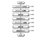
- FIG. 10 is a flowchart of a design support processing procedure of the design support apparatus 600 according to the second embodiment.
- layout data is acquired (step S1001).
- the layout data acquired here is layout data that has been initially arranged.
- the generation unit 601 builds a clock tree on the acquired layout data (step S1002).
- the layout data 400 described above is an example of layout data in which a clock tree is constructed.
- a replacement process is executed by the detection unit 602 to the replacement unit 606 (step S1003), and a replacement result is output by the output unit 607 (step S1004).
- the layout data 700 described above is a replacement result.
- the clock skew is adjusted by the generation unit 601 (step S1005).
- the layout data 800 described above is an example in which the clock skew of the layout data 700 is adjusted.
- the detection unit 602 to the replacement unit 606 execute replacement processing (step S1006), the output unit 607 outputs the replacement result (step S1007), and the series of processing ends.
- the layout data 900 described above is a replacement result.
- the replacement process steps S1003 / S1006) will be described with reference to FIG.
- FIG. 11 is a flowchart showing a detailed processing procedure of the replacement processing (steps S1003 / S1006) shown in FIG.
- the detection unit 602 detects a clock path whose clock buffer cell has one gate stage (step S1101), and determines whether there is an unselected clock path (step S1102).
- step S1106 If it is determined that i ⁇ N (step S1106: Yes), the selection unit 603 selects the i-th FF (step S1107), and the specification unit 604 specifies the input source clock buffer (step S1108). ). Then, the number of gate stages from the clock supply source to the clock buffer is detected (step S1109), and the determination unit 605 determines whether the number of gate stages from the clock supply source to the clock buffer is an even number (step S1110). Based on the number of gate stages from the clock supply source to the clock buffer, it is determined whether the specified clock buffer outputs the clock signal with positive logic or inverted logic.
- step S1106 determines whether i ⁇ N is not satisfied. If it is determined that i ⁇ N is not satisfied (step S1106: NO), the process proceeds to step S1102. On the other hand, when it is determined that there is no unselected clock path (step S1102: No), the process proceeds to step S1004 (or step S1007).
- the design support method, the design support apparatus, the design support program, the FF connected to the clock path configured in the clock buffer 301 having one gate stage is the clock that is the input source from the clock supply source.
- the first FF 201 or the second FF 202 is replaced based on the number of gate stages up to the buffer.
- the FF connected to the clock path whose gate stage number is optimized is automatically replaced with an appropriate FF corresponding to the waveform of the clock signal. Therefore, layout data having a clock path having the minimum number of gate stages can be easily designed, and power consumption can be reduced.
- the number of gate stages from the clock supply source to the clock buffer that is the input source of the FF is an even number, it is replaced with the first FF, and if it is an odd number, it is replaced with the second FF.
- FF can be easily replaced according to the number of gate stages, and low power consumption can be achieved.
- the clock tree is constructed with a minimum number of gate stages, thereby reducing power consumption. be able to.
- the skew is adjusted with the minimum number of gate stages, thereby reducing power consumption. it can.
- the clock signal When the clock signal is output with inverted logic, if the number of gate stages from the clock start point specified by the user to the clock buffer that is the input source of the FF is an odd number, it is replaced with the first FF. And the second FF. Thus, it can be easily determined whether or not the clock signal from the clock supply source is output in positive logic according to the number of gate stages. Therefore, FFs can be easily replaced according to the number of gate stages, and low power consumption can be achieved. Furthermore, since only the number of gate stages from the designated location is searched, the search time can be shortened.
- the clock path is provided by including the clock path, the FF connected to the clock path, and the clock buffer having one gate stage as the input source of the FF. It is configured with a minimum number of gate stages, and low power consumption can be achieved.
- the FF captures data at the rising edge of the clock signal based on the number of gate stages from the clock supply source to the clock buffer that is the input source of the FF, or captures data at the falling edge, thereby minimizing the gate.
- a clock path is configured by the number of stages, and low power consumption can be achieved.
- the design support method described in the present embodiment can be realized by executing a program prepared in advance on a computer such as a personal computer or a workstation.
- the design support program is recorded on a computer-readable recording medium such as a hard disk, a flexible disk, a CD-ROM, an MO, and a DVD, and is executed by being read from the recording medium by the computer.
- the design support program may be distributed via a network such as the Internet.
Landscapes
- Physics & Mathematics (AREA)
- Engineering & Computer Science (AREA)
- Theoretical Computer Science (AREA)
- Nonlinear Science (AREA)
- General Engineering & Computer Science (AREA)
- General Physics & Mathematics (AREA)
- Design And Manufacture Of Integrated Circuits (AREA)
Abstract
設計支援装置は、ゲート段数1段の反転論理であるクロックバッファを用いてクロックツリーが構築またはスキューが調整されたレイアウトデータ内から、クロック供給源であるクロック入力端子からのクロック信号を伝播し、当該クロックバッファのみのクロックパス(801)を検出し、クロックパス(801)に接続されているFF1~FF3を順次選択し、クロック供給源から選択されたFFの入力元であるクロックバッファまでのゲート段数に基づいて、クロック供給源からのクロック信号を正論理で出力するか反転論理で出力するかを判断し、判断結果に基づいて、選択されたFF1~FF3を、クロック信号の立ち上がりエッジでデータを取り込むFFか、立ち下がりエッジでデータを取り込むFFかに置換する。
Description
本発明は、レイアウトデータの設計を支援する設計支援方法、設計支援装置、設計支援プログラム、および半導体集積回路に関する。
従来、半導体集積回路の消費電力を低減させる技術として、動作に必要ではない回路へのクロック信号または電源電圧の供給を止めるクロックゲーティングやパワーゲーティング(以下、「第1の従来技術」と称す。)が知られている。さらに、半導体集積回路の消費電力を低減させる技術として、低電圧化や多電源化(以下、「第2の従来技術」と称す。)が知られている。
また、従来、クロックスキューの低減およびノイズを減少させる技術として、クロック信号の立ち上がりエッジに同期してデータを取り込むデータ保持素子(以下、「第1のFF(Flip Flop)」と称す。)やクロック信号の立ち下がりエッジに同期してデータを取り込むデータ保持素子(以下、「第2のFF」と称す。)を用いること(以下、第3の従来技術と称す。)が知られている(たとえば、下記特許文献1~3を参照。)。
しかしながら、第1の従来技術では、クロックパスを常時動作させる必要がある回路では適用することが出来ないという問題点があった。また、第2の従来技術では、クロックパスを常に高速で動作させる場合、電源電圧を下げるために半導体集積回路内の動作が遅くなるため、電源電圧を下げることができないという問題点があった。
また、第3の従来技術では、ゲート段数が複数段であるクロックバッファを用いて第1のFFおよび第2のFFに入力されるクロック信号を伝播している。そのため、正論理が必要な場合、必ずゲート段数2段、もしくはゲート段数2段以上の偶数段の正論理であるクロックバッファが挿入されるため、クロックパス上のゲート段数が増大してしまう問題点があった。
上述した課題を解決するため、本発明の一観点によれば、レイアウトデータ内から、クロック供給源からのクロック信号を伝播し、クロックバッファがゲート段数1段の反転論理であるクロックパスを検出する検出手段と、前記検出手段により検出されたクロックパスに接続されているデータ保持素子を順次選択する選択手段と、前記選択手段によりデータ保持素子が選択される都度、前記データ保持素子の入力元であるクロックバッファを特定する特定手段と、前記クロック供給源から前記特定手段により特定されたクロックバッファまでのゲート段数に基づいて前記クロックバッファが前記クロック供給源からの前記クロック信号を正論理で出力するか、反転論理で出力するかを判断する判断手段と、前記判断手段により判断された判断結果に基づいて、前記データ保持素子を、前記クロック信号の立ち上がりに同期してデータを取り込む第1のデータ保持素子、または前記クロック信号の立ち下がりエッジに同期してデータを取り込む第2のデータ保持素子に置換する置換手段と、前記置換手段により置換された置換結果を出力する出力手段と、を備える設計支援方法が提供される。
本設計支援方法、設計支援装置、設計支援プログラム、および半導体集積回路によればゲート段数1段のクロックバッファを用いて、クロックパス上のゲート段数を容易に最適化して低消費電力化を図ることができるという効果を奏する。
以下に添付図面を参照して、本発明の実施の形態による設計支援方法、設計支援装置、設計支援プログラム、および半導体集積回路について説明する。
本発明の実施形態では、クロック供給源からのクロック信号を伝播するクロックパスに接続されているデータ保持素子の入力元であるクロックバッファが、ゲート段数1段の反転論理により構成されている。なお、本実施の形態ではデータ保持素子としてFFを用いて説明する。そして、各FFは、クロック供給源から当該FFの入力元であるクロックバッファまでのゲート段数が偶数段であれば、上述した第1のFFであり、奇数段であれば、上述した第2のFFである。
まず、実施の形態1では、ゲート段数1段のクロックバッファによりゲート段数が最適化されたクロックパスを有する半導体集積回路について説明する。つぎに、実施の形態2では、上述したクロックパスに接続されているFFを、第1のFFまたは第2のFFに置換する設計支援装置について説明する。まず、図1にて実施の形態1の概要を示す。
(実施の形態1)
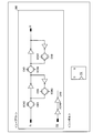
図1は、実施の形態1にかかる半導体集積回路の一例を示す説明図である。半導体集積回路100は、クロック入力端子から入力されるクロック信号を伝播するクロックパス101と、クロックパス101に接続されているFF1~FF3と、ゲート段数1段であり、クロックパス101上のBUF1~BUF5により構成されている。実施の形態1では、クロック入力端子をクロック供給源として説明するが、クロック信号を生成するクロック生成回路などがクロック供給源であってもよい。
図1は、実施の形態1にかかる半導体集積回路の一例を示す説明図である。半導体集積回路100は、クロック入力端子から入力されるクロック信号を伝播するクロックパス101と、クロックパス101に接続されているFF1~FF3と、ゲート段数1段であり、クロックパス101上のBUF1~BUF5により構成されている。実施の形態1では、クロック入力端子をクロック供給源として説明するが、クロック信号を生成するクロック生成回路などがクロック供給源であってもよい。
BUF1~BUF5は、ゲート段数1段の反転論理であるクロックバッファである。半導体集積回路100では、FF1~3の入力元であるクロックバッファがクロック入力端子からのクロック信号を正論理で出力するか否かに応じて、各FFが、クロック信号の立ち上がりエッジに同期してデータを取り込むか、立ち下がりエッジに同期してデータを取り込む。
まず、FF1を例に挙げると、クロック入力端子からFF1の入力元であるBUF3までのゲート段数は3段である。したがって、FF1は、第2のFFである。つぎに、FF2を例に挙げると、クロック入力端子からFF2の入力元であるBUF4までのゲート段数は4段である。したがって、FF2は、第1のFFである。
最後に、FF3を例に挙げると、クロック入力端子からFF3の入力元であるBUF5までのゲート段数は5段である。したがって、FF3は、第2のFFである。これにより、ゲート段数1段のクロックバッファによりクロックパスが構成されることで、最小限のゲート段数でクロックパスが構成される。したがって、半導体集積回路の低消費電力化を図ることができる。
(実施の形態2)
つぎに、実施の形態2では、クロックバッファがゲート段数1段であるクロックパスに接続されているFFを、FFの入力元であるクロックバッファがクロック供給源からのクロック信号を正論理で出力するか否かにより第1のFFまたは第2のFFに置換する。これにより、クロックパス上のゲート段数を可能な限り削減し、低消費電力化を図ることができる。まず、図2-1および図2-2により第1のFFおよび第2のFFの一例を示す。
つぎに、実施の形態2では、クロックバッファがゲート段数1段であるクロックパスに接続されているFFを、FFの入力元であるクロックバッファがクロック供給源からのクロック信号を正論理で出力するか否かにより第1のFFまたは第2のFFに置換する。これにより、クロックパス上のゲート段数を可能な限り削減し、低消費電力化を図ることができる。まず、図2-1および図2-2により第1のFFおよび第2のFFの一例を示す。
図2-1は、第1のFFの一例を示す説明図である。<レイアウトデータ>では、第1のFF201のレイアウトデータを示している。第1のFF201は、クロック信号の立ち上がりエッジに同期してデータを取り込むFFの一例である。第1のFF201は、レイアウトデータであるが、理解の容易化のために回路図で示されている。
第1のFF201では、CKに入力されるクロック信号の立ち上がりエッジに同期してDに入力されるデータを内部に取り込み、Qから出力する。<シンボル>では、第1のFF201のシンボルを示している。後述する半導体集積回路のレイアウトデータ内では、第1のFF201をシンボルで表記する。なお、第1のFF201は、ライブラリ内に記述され、記憶装置またはアクセス可能な外部のコンピュータの記憶装置に記憶されている。つぎに、図2-2にて第2のFFを示す。
図2-2は、第2のFFの一例を示す説明図である。<レイアウトデータ>では、第2のFF202のレイアウトデータを示している。第2のFF202は、クロック信号の立ち下がりエッジに同期してデータを取り込むFFの一例である。第2のFF202は、レイアウトデータであるが、理解の容易化のために回路図で示されている。
第2のFF202では、/CKに入力されるクロック信号の立ち下がりエッジに同期してDに入力されるデータを内部に取り込み、Qから出力する。<シンボル>では、第2のFF202のシンボルを示している。後述する半導体集積回路のレイアウトデータ内では、第2のFF202をシンボルで表記する。なお、第2のFF202は、ライブラリ内に記述され、記憶装置またはアクセス可能な外部のコンピュータの記憶装置に記憶されている。つぎに、図3にてクロックバッファの例を示す。
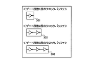
図3は、クロックバッファの例を示す説明図である。クロックバッファ301は、ゲート段数1段により構成されている。クロックバッファ301は、反転論理である。つぎに、クロックバッファ302は、ゲート段数2段により構成されている。クロックバッファ302は、正論理である。そして、クロックバッファ303は、ゲート段数3段により構成されている。クロックバッファ303は、反転論理である。
従来では、反転論理が必要な場合、クロックバッファ303が利用されていたが、本実施の形態では、クロックバッファ301が利用される。したがって、本実施の形態では、クロックバッファ301によりクロックツリーが構築またはスキューが調整される。
(設計対象のレイアウトデータ)
図4は、設計対象のレイアウトデータを示す説明図である。レイアウトデータ400は、クロック入力端子へ入力されるクロック信号を伝播するクロックパス401と、クロックパス401に接続されているFF1~FF3と、組み合わせ回路と、クロックバッファ301であるBUF1~BUF4を含む構成である。
図4は、設計対象のレイアウトデータを示す説明図である。レイアウトデータ400は、クロック入力端子へ入力されるクロック信号を伝播するクロックパス401と、クロックパス401に接続されているFF1~FF3と、組み合わせ回路と、クロックバッファ301であるBUF1~BUF4を含む構成である。
レイアウトデータ400は、理解の容易化のために回路図で示されているが、実際には、物理情報である。たとえば、FF1~FF3、およびBUF1~BUF4は、インスタンス名であり、各FFを特定するための名前である。そして、物理情報では、配置位置を示す座標と、セル同士の接続関係と、各セルを構成する層情報と、配線幅などの情報を有している。たとえば、FF1が第1のFF201に置換されることは、実際には、物理情報内のFF1のセル名が書き換えられていることを示す。
まず、レイアウトデータ400では、FF1~FF3が、第1のFF201である。実際には、FF1~FF3は、第1のFF201および第2のFF202のいずれのFFであってもよい。または、たとえば、FF1~FF3は、第1のFF201および第2のFF202と同一形状、同一面積であるダミーのFFであってもよい。
つぎに、BUF1~BUF4は、すべて上述したクロックバッファ301である。そして、レイアウトデータ400では、クロック入力端子をクロック供給源として説明するが、これに限らない。たとえば、クロック信号を生成するクロック生成回路をクロック供給源としてもよい。
本実施の形態2にかかる設計支援装置により、FF1~FF3が、第1のFF201、または第2のFF202に置換される。なお、レイアウトデータ400は、記憶装置またはアクセス可能な外部のコンピュータの記憶装置に記憶されている。
(設計支援装置のハードウェア構成)
図5は、実施の形態2にかかる設計支援装置のハードウェア構成例を示すブロック図である。図5において、設計支援装置は、CPU(Central Processing Unit)501と、ROM(Read‐Only Memory)502と、RAM(Random Access Memory)503と、磁気ディスクドライブ504と、磁気ディスク505と、光ディスクドライブ506と、光ディスク507と、ディスプレイ508と、I/F(Interface)509と、キーボード510と、マウス511と、スキャナ512と、プリンタ513と、を備えている。また、各構成部はバス500によってそれぞれ接続されている。
図5は、実施の形態2にかかる設計支援装置のハードウェア構成例を示すブロック図である。図5において、設計支援装置は、CPU(Central Processing Unit)501と、ROM(Read‐Only Memory)502と、RAM(Random Access Memory)503と、磁気ディスクドライブ504と、磁気ディスク505と、光ディスクドライブ506と、光ディスク507と、ディスプレイ508と、I/F(Interface)509と、キーボード510と、マウス511と、スキャナ512と、プリンタ513と、を備えている。また、各構成部はバス500によってそれぞれ接続されている。
ここで、CPU501は、設計支援装置の全体の制御を司る。ROM502は、ブートプログラムなどのプログラムを記憶している。RAM503は、CPU501のワークエリアとして使用される。磁気ディスクドライブ504は、CPU501の制御にしたがって磁気ディスク505に対するデータのリード/ライトを制御する。磁気ディスク505は、磁気ディスクドライブ504の制御で書き込まれたデータを記憶する。
光ディスクドライブ506は、CPU501の制御にしたがって光ディスク507に対するデータのリード/ライトを制御する。光ディスク507は、光ディスクドライブ506の制御で書き込まれたデータを記憶したり、光ディスク507に記憶されたデータをコンピュータに読み取らせたりする。
ディスプレイ508は、カーソル、アイコンあるいはツールボックスをはじめ、文書、画像、機能情報などのデータを表示する。このディスプレイ508は、たとえば、CRT、TFT液晶ディスプレイ、プラズマディスプレイなどを採用することができる。
I/F509は、通信回線を通じてLAN(Local Area Network)、WAN(Wide Area Network)、インターネットなどのネットワーク514に接続され、このネットワーク514を介して他の装置に接続される。そして、I/F509は、ネットワーク514と内部のインターフェースを司り、外部装置からのデータの入出力を制御する。I/F509には、たとえばモデムやLANアダプタなどを採用することができる。
キーボード510は、文字、数字、各種指示などの入力のためのキーを備え、データの入力をおこなう。また、タッチパネル式の入力パッドやテンキーなどであってもよい。マウス511は、カーソルの移動や範囲選択、あるいはウィンドウの移動やサイズの変更などをおこなう。ポインティングデバイスとして同様に機能を備えるものであれば、トラックボールやジョイスティックなどであってもよい。
スキャナ512は、画像を光学的に読み取り、設計支援装置内に画像データを取り込む。なお、スキャナ512は、OCR(Optical Character Reader)機能を持たせてもよい。また、プリンタ513は、画像データや文書データを印刷する。プリンタ513には、たとえば、レーザプリンタやインクジェットプリンタを採用することができる。
(設計支援装置の機能的構成)
図6は、実施の形態2にかかる設計支援装置の機能的構成例を示すブロック図である。設計支援装置600は、生成部601と、検出部602と、選択部603と、特定部604と、判断部605と、置換部606と、出力部607と、を含む構成である。設計支援装置600の制御部となる機能(生成部601~出力部607)は、具体的には、たとえば、図5に示したROM502、RAM503、磁気ディスク505、光ディスク507などの記憶装置に記憶されたプログラムをCPU501に実行させることにより、または、I/F509により、その機能を実現する。
図6は、実施の形態2にかかる設計支援装置の機能的構成例を示すブロック図である。設計支援装置600は、生成部601と、検出部602と、選択部603と、特定部604と、判断部605と、置換部606と、出力部607と、を含む構成である。設計支援装置600の制御部となる機能(生成部601~出力部607)は、具体的には、たとえば、図5に示したROM502、RAM503、磁気ディスク505、光ディスク507などの記憶装置に記憶されたプログラムをCPU501に実行させることにより、または、I/F509により、その機能を実現する。
まず、生成部601は、少なくとも指定されたクロックパスにゲート段数が1段の反転論理であるクロックバッファのセルを用いてクロックツリーを構築することによりレイアウトデータを生成する機能を有する。
具体的には、たとえば、CPU501が、指定されたクロックパスがクロックバッファ301のみでクロックツリーを構築するように指定し、既存のクロックツリーを構築するツールを実行することでクロックツリー構築後のレイアウトデータを生成する。なお、生成結果は、RAM503、磁気ディスク505、光ディスク507などの記憶装置に記憶される。
生成結果が、たとえば、上述したレイアウトデータ400である。これにより、ゲート段数1段のクロックバッファを用いてクロックツリーを構築することで、クロックパス上のゲート段数が最適化される。したがって、クロックパス上のゲート段数を可能な限り削減し、低消費電力化を図ることができる。
つぎに、検出部602は、生成部601により生成されたレイアウトデータ内から、クロック供給源からのクロック信号を伝播し、クロックバッファがゲート段数1段の反転論理であるクロックパスを検出する。具体的には、たとえば、CPU501が、記憶装置にアクセスしてレイアウトデータ400からクロックバッファ301のみを使用しているクロックパスを検出する。また、たとえば、予め利用者により指定されているクロックパスを検出することとしてもよい。
レイアウトデータ400では、クロックバッファがゲート段数1段の反転論理であるクロックパスとして、クロックパス401が検出される。なお、検出結果は、一旦RAM503、磁気ディスク505、光ディスク507などの記憶装置に記憶される。
そして、選択部603は、検出部602により検出されたクロックパスに接続されているFFを順次選択する機能を有する。具体的には、たとえば、CPU501が、レイアウトデータ400からクロックパス401に接続されているFFを順次選択する。たとえば、まず、FF1が選択され、つぎに、FF2が選択され、最後に、FF3が選択される。
特定部604は、選択部603により選択されたFFの入力元であるクロックバッファを特定する機能を有する。具体的には、たとえば、クロックパス401に接続されているFF1を例に挙げると、CPU501が、レイアウトデータ400からFF1のCKに接続されているネットを検出する。そして、検出したネットが出力先として接続されているクロックバッファをFF1の入力元として特定する。したがって、FF1の入力元としてBUF3が特定される。
判断部605は、クロック供給源から特定部604により特定されたクロックバッファまでのゲート段数に基づいて、当該クロックバッファがクロック供給源からのクロック信号を正論理で出力するか否かを判断する機能を有する。
具体的には、たとえば、CPU501が、記憶装置にアクセスしてレイアウトデータ400を読み出し、クロック入力端子から特定されたクロックバッファまでのゲート段数を検出する。そして、検出されたゲート段数が偶数段の場合、特定されたクロックバッファがクロック信号を正論理で出力すると判断し、奇数段の場合、特定されたクロックバッファがクロック信号を反転論理で出力すると判断する。
レイアウトデータ400内のFF1の入力元であるBUF3を例に挙げると、クロック入力端子からBUF3までのゲート段数は、3段である。したがって、BUF3は、クロック入力端子からのクロック信号を反転論理で出力すると判断される。なお、判断結果は、一旦、RAM503、磁気ディスク505、光ディスク507などの記憶装置に記憶される。
つぎに、置換部606は、判断部605により正論理で出力すると判断された場合、選択されたFFを第1のFFに置換し、反転論理で出力すると判断された場合、第2のFFに置換する。
具体的には、たとえば、CPU501が、記憶装置にアクセスしてレイアウトデータ400と判断結果を読み出す。そして、判断結果が偶数段の場合、レイアウトデータ400内の選択されたFFを第1のFF201に置換し、奇数段の場合、レイアウトデータ400内の選択されたFFを第2のFF202に置換する。
レイアウトデータ400内のFF1を例に挙げると、上述したようにFF1の入力元であるBUF3は、クロック入力端子からのクロック信号を反転論理で出力すると判断されているため、FF1は第2のFF202に置換される。
つぎに、出力部607は、置換部606により置換された置換結果を出力する。具体的には、たとえば、CPU501が、レイアウトデータを出力する。出力形式としては、たとえば、ディスプレイ508への表示、プリンタ513への印刷出力、I/F509による外部装置への送信がある。また、RAM503、磁気ディスク505、光ディスク507などの記憶領域に記憶することとしてもよい。図5にて出力されたレイアウトデータを示す。
図7は、レイアウトデータ400内のFFが置換されて出力された例を示す説明図である。レイアウトデータ700は、クロック入力端子からのクロック信号を伝播するクロックパス401と、クロックパス401に接続されている第2のFF202であるFF1およびFF2と、クロックパス401に接続されている第1のFF201であるFF3と、クロックバッファであるBUF1~BUF4である。
これにより、ゲート段数が最適化されているクロックパスに接続されているFFが、クロック信号の波形に応じた適切なFFに自動で置換される。したがって、最小限のゲート段数であるクロックパスを有するレイアウトデータを容易に設計でき、低消費電力化を図ることができる。
また、生成部601は、ゲート段数1段の反転論理であるクロックバッファのみを用いて少なくとも指定されたクロックパスのスキューを調整することによりレイアウトデータを生成する機能を有する。具体的には、たとえば、CPU501が、クロックバッファ301のみでスキューを調整するように指定し、既存のスキューを調整するツールを実行することでレイアウトデータ700からスキューを調整済のレイアウトデータを生成する。なお、生成結果は、RAM503、磁気ディスク505、光ディスク507などの記憶装置に記憶される。図8にて生成結果を示す。
図8は、スキューを調整済のレイアウトデータを示す説明図である。レイアウトデータ800は、BUF5とBUF6を含み、その他はレイアウトデータ700で示した構成と同一構成である。これにより、ゲート段数1段のクロックバッファを用いてスキューが調整されることで、クロックパス上のゲート段数が最適化される。したがって、クロックパス上のゲート段数を可能な限り削減し、低消費電力化を図ることができる。
図6に戻って、検出部602は、生成部601により生成されたスキューを調整済のレイアウトデータ800内から、クロック供給源からのクロック信号を伝播し、クロックバッファがゲート段数1段の反転論理であるクロックパスを検出する。具体的には、たとえば、CPU501が、記憶装置にアクセスしてレイアウトデータ800からクロックバッファ301のみを使用しているクロックパスを検出する。また、たとえば、利用者により予め指定されているクロックパスを検出することとしてもよい。
レイアウトデータ800では、クロックバッファがゲート段数1段の反転論理であるクロックパスとして、クロックパス801が検出される。なお、検出結果は、一旦RAM503、磁気ディスク505、光ディスク507などの記憶装置に記憶される。
つぎに、再度、上述した選択部603~出力部607の機能により、レイアウトデータ800内のクロックパス801に接続されているFFが、第1のFF201または第2のFF202に置換される。図9にて置換結果を示す。
図9は、レイアウトデータ800内のFFが置換されて出力された例を示す説明図である。レイアウトデータ900は、クロック入力端子からFF2の入力元であるBUF5までのゲート段数が、4段である。そのため、FF2が第1のFF201に置換されている。なお、その他の構成は、レイアウトデータ800と同一構成である。これにより、スキューを調整済のレイアウトデータであってもFFを容易に置換することができ、クロックパス上のゲート段数を最小限に抑え低消費電力化を図ることができる。
実施の形態2では、クロック供給源からFFの入力元であるクロックバッファまでのゲート段数に基づいて、各FFが第1のFF201または第2のFF202に決定されている。さらに、たとえば、利用者が指定した箇所からFFの入力元であるクロックバッファまでのゲート段数に基づいて、各FFが第1のFF201または第2のFF202に決定されることとしてもよい。ここで、特製されたクロックバッファがクロック供給源からのクロック信号を反転論理で出力するか正論理で出力かを判断するために利用者が指定した箇所をクロックの起点とする。そして、クロックの起点は、クロック供給源からのクロック信号を正論理で出力するか反転論理で出力するかがあらかじめ決定していることとして説明する。
まず、クロック供給源からのクロック信号を正論理で伝播している箇所が利用者によりクロック起点として指定された場合の判断部605の機能について説明する。判断部605は、クロックの起点から特定されたクロックバッファまでのゲート段数が偶数段のときにクロック供給源からのクロック信号を正論理で出力すると判断する。そして、判断部605は、指定された箇所から特定されたクロックバッファまでのゲート段数が奇数段のときにクロック供給源からのクロック信号を反転論理で出力すると判断する。なお、ゲート段数の検出については、上述した判断部605の処理と同一処理であるため詳細な説明を省略する。
つぎに、クロック供給源からのクロック信号を反転論理で伝播している箇所が利用者によりクロック起点として指定された場合の判断部605の機能について説明する。判断部605は、クロックの起点から特定されたクロックバッファまでのゲート段数が奇数段のときにクロック供給源からのクロック信号を正論理で出力すると判断する。そして、判断部605は、指定された箇所から特定されたクロックバッファまでのゲート段数が偶数段のときにクロック供給源からのクロック信号を反転論理で出力すると判断する。なお、ゲート段数の検出については、上述した判断部605の処理と同一処理であるため詳細な説明を省略する。
(設計支援装置600の設計支援処理手順)
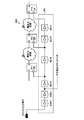
図10は、実施の形態2にかかる設計支援装置600の設計支援処理手順を示すフローチャートである。まず、レイアウトデータを取得する(ステップS1001)。ここで取得されるレイアウトデータは、初期配置済のレイアウトデータである。つぎに、生成部601により、取得されたレイアウトデータにクロックツリーを構築する(ステップS1002)。上述したレイアウトデータ400が、クロックツリーが構築されたレイアウトデータの例である。
図10は、実施の形態2にかかる設計支援装置600の設計支援処理手順を示すフローチャートである。まず、レイアウトデータを取得する(ステップS1001)。ここで取得されるレイアウトデータは、初期配置済のレイアウトデータである。つぎに、生成部601により、取得されたレイアウトデータにクロックツリーを構築する(ステップS1002)。上述したレイアウトデータ400が、クロックツリーが構築されたレイアウトデータの例である。
つづいて、検出部602~置換部606により、置換処理を実行し(ステップS1003)、出力部607により、置換結果を出力する(ステップS1004)。たとえば、上述したレイアウトデータ700が、置換結果である。そして、生成部601により、クロックスキューを調整する(ステップS1005)。上述したレイアウトデータ800が、レイアウトデータ700のクロックスキューが調整された例である。つぎに、検出部602~置換部606により、置換処理を実行し(ステップS1006)、出力部607により、置換結果を出力し(ステップS1007)、一連の処理を終了する。上述したレイアウトデータ900が、置換結果である。つぎに、図11にて置換処理(ステップS1003/S1006)について説明する。
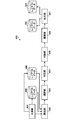
図11は、図10に示した置換処理(ステップS1003/S1006)の詳細な処理手順を示すフローチャートである。まず、検出部602により、クロックバッファセルがゲート段数1段であるクロックパスを検出する(ステップS1101)、未選択のクロックパスがあるか否かを判断する(ステップS1102)。
未選択のクロックパスがあると判断された場合(ステップS1102:Yes)、未選択のクロックパスを1つ選択し(ステップS1103)、i=1とする(ステップS1104)。つぎに、N=クロックパスに接続されているFFの総数とし(ステップS1105)、i≦Nであるか否かを判断する(ステップS1106)。
i≦Nであると判断された場合(ステップS1106:Yes)、選択部603により、i番目のFFを選択し(ステップS1107)、特定部604により、入力元のクロックバッファを特定する(ステップS1108)。そして、クロック供給源からクロックバッファまでのゲート段数を検出し(ステップS1109)、判断部605により、クロック供給源からクロックバッファまでのゲート段数が偶数段か否かを判断する(ステップS1110)。クロック供給源からクロックバッファまでのゲート段数に基づいて、特定されたクロックバッファがクロック信号を正論理で出力するか、反転論理で出力するかが判断される。
偶数段であると判断された場合(ステップS1110:Yes)、置換部606により、i番目のFFを第1のFFに置換し(ステップS1111)、i=i+1とし(ステップS1113)、ステップS1106に戻る。一方、偶数段でない(奇数段である)と判断された場合(ステップS1110:No)、置換部606により、i番目のFFを第2のFFに置換し(ステップS1112)、上述したステップS1113へ移行する。
一方、i≦Nでないと判断された場合(ステップS1106:No)、ステップS1102へ移行する。さらに、一方、未選択のクロックパスがないと判断された場合(ステップS1102:No)、ステップS1004(またはステップS1007)へ移行する。
以上説明したように、設計支援方法、設計支援装置、設計支援プログラム、ゲート段数1段のクロックバッファ301に構成されているクロックパスに接続されているFFが、クロック供給源から入力元であるクロックバッファまでのゲート段数に基づいて第1のFF201または第2のFF202に置換される。
これにより、ゲート段数が最適化されているクロックパスに接続されているFFが、クロック信号の波形に応じた適切なFFに自動で置換される。したがって、最小限のゲート段数であるクロックパスを有するレイアウトデータを容易に設計でき、低消費電力化を図ることができる。
また、クロック供給源からFFの入力元であるクロックバッファまでのゲート段数が偶数段の場合、第1のFFに置換し、奇数段の場合、第2のFFに置換する。これにより、ゲート段数に応じて容易にFFを置換でき、低消費電力化を図ることができる。
また、ゲート段数1段の反転論理であるクロックバッファのみを用いてクロックツリーが構築されたレイアウトデータを自動生成することにより、最小限のゲート段数によりクロックツリーが構築され、低消費電力化を図ることができる。
また、ゲート段数1段の反転論理であるクロックバッファのみを用いてスキューが調整されたレイアウトデータを自動生成することにより、最小限のゲート段数によりスキューが調整され、低消費電力化を図ることができる。
また、クロック供給源からのクロック信号を正論理で出力すると利用者により指定されたクロックの起点からFFの入力元であるクロックバッファまでのゲート段数が偶数段の場合、第1のFFに置換し、奇数段の場合、第2のFFに置換する。これにより、ゲート段数に応じてクロック供給源からのクロック信号を正論理で出力するか否かが容易に判断できる。したがって、ゲート段数に応じて容易にFFを置換でき、低消費電力化を図ることができる。さらに、指定された箇所からのゲート段数を検索するのみであるため、検索時間を短縮することができる。
また、クロック信号を反転論理で出力すると利用者により指定されたクロックの起点からFFの入力元であるクロックバッファまでのゲート段数が奇数段の場合、第1のFFに置換し、偶数段の場合、第2のFFに置換する。これにより、ゲート段数に応じてクロック供給源からのクロック信号を正論理で出力するか否かが容易に判断できる。したがって、ゲート段数に応じて容易にFFを置換でき、低消費電力化を図ることができる。さらに、指定された箇所からのゲート段数を検索するのみであるため、検索時間を短縮することができる。
以上説明したように、半導体集積回路によれば、クロックパスと、クロックパスに接続されているFFと、FFの入力元であり、ゲート段数1段のクロックバッファとを備えることで、クロックパスが最小限のゲート段数で構成され、低消費電力化を図ることができる。
さらに、FFは、クロック供給源から当該FFの入力元であるクロックバッファまでのゲート段数に基づいてクロック信号の立ち上がりエッジでデータを取り込むか、立ち下がりエッジでデータを取り込むことで、最小限のゲート段数でクロックパスが構成され、低消費電力化を図ることができる。
なお、本実施形態で説明した設計支援方法は、予め用意されたプログラムをパーソナル・コンピュータやワークステーション等のコンピュータで実行することにより実現することができる。本設計支援プログラムは、ハードディスク、フレキシブルディスク、CD-ROM、MO、DVD等のコンピュータで読み取り可能な記録媒体に記録され、コンピュータによって記録媒体から読み出されることによって実行される。また本設計支援プログラムは、インターネット等のネットワークを介して配布してもよい。
201 第1のFF
202 第2のFF
301 クロックバッファ
400,700,800,900 レイアウトデータ
202 第2のFF
301 クロックバッファ
400,700,800,900 レイアウトデータ
Claims (10)
- 複数のデータ保持素子と、クロック供給源からのクロック信号を前記複数のデータ保持素子へ伝播するクロックパスと、を備える半導体集積回路を設計する設計支援方法であって、
コンピュータが、
前記半導体集積回路のレイアウトデータ内から、前記クロック信号を伝播し、クロックバッファがゲート段数1段の反転論理であるクロックパスを検出する検出工程、
前記検出工程により検出されたクロックパスに接続されているデータ保持素子を順次選択する選択工程、
前記選択工程によりデータ保持素子が選択される都度、前記データ保持素子の入力元であるクロックバッファを特定する特定工程、
前記クロック供給源から前記特定工程により特定されたクロックバッファまでのゲート段数に基づいて、前記クロックバッファが前記クロック供給源からの前記クロック信号を正論理で出力するか、反転論理で出力するかを判断する判断工程、
前記判断工程により判断された判断結果に基づいて、前記データ保持素子を、前記クロック信号の立ち上がりエッジに同期してデータを取り込む第1のデータ保持素子、または前記クロック信号の立ち下がりエッジに同期してデータを取り込む第2のデータ保持素子に置換する置換工程、
前記置換工程により置換された置換結果を出力する出力工程、
を実行することを特徴とする設計支援方法。 - 前記判断工程は、
前記ゲート段数が、偶数段の場合、前記特定工程により特定されたクロックバッファが前記クロック信号を正論理で出力すると判断し、奇数段の場合、反転論理で出力すると判断し、
前記置換工程は、
前記判断工程により正論理で出力すると判断された場合、前記データ保持素子を前記第1のデータ保持素子に置換し、反転論理で出力すると判断された場合、前記第2のデータ保持素子に置換することを特徴とする請求項1に記載の設計支援方法。 - 前記コンピュータが、
ゲート段数1段の反転論理であるクロックバッファのみを用いて指定されたクロックパスにクロックツリーを構築することによりレイアウトデータを生成する生成工程、を実行し、
前記検出工程は、
前記生成工程により生成されたレイアウトデータ内から、クロック供給源からのクロック信号を伝播し、クロックバッファがゲート段数1段の反転論理であるクロックパスを検出することを特徴とする請求項2に記載の設計支援方法。 - 前記生成工程は、
ゲート段数1段の反転論理であるクロックバッファのみを用いて指定されたクロックパスのスキューを調整することによりレイアウトデータを生成し、
前記検出工程は、
前記生成工程により生成されたレイアウトデータ内から、クロック供給源からのクロック信号を伝播し、クロックバッファがゲート段数1段の反転論理であるクロックパスを検出することを特徴とする請求項3に記載の設計支援方法。 - 前記判断工程は、
クロックの起点として指定された箇所が前記クロック供給源からのクロック信号を正論理で出力する場合、前記クロックの起点から前記クロックバッファまでのゲート段数が、偶数段の場合、前記クロックバッファが前記クロック信号を正論理で出力すると判断し、奇数段の場合、反転論理で出力すると判断し、
前記置換工程は、
前記判断工程により正論理で出力すると判断された場合、前記データ保持素子を前記第1のデータ保持素子に置換し、反転論理で出力すると判断された場合、前記第2のデータ保持素子に置換することを特徴とする請求項4に記載の設計支援方法。 - 前記判断工程は、
クロックの起点として指定された箇所が前記クロック供給源からのクロック信号を反転論理で伝播している場合、前記クロックの起点から前記クロックバッファまでのゲート段数が、偶数段の場合、前記クロックバッファが前記クロック信号を反転論理で出力すると判断し、奇数段の場合、正論理で出力すると判断し、
前記置換工程は、
前記判断工程により正論理で出力すると判断された場合、前記データ保持素子を前記第1のデータ保持素子に置換し、反転論理で出力すると判断された場合、前記第2のデータ保持素子に置換することを特徴とする請求項5に記載の設計支援方法。 - レイアウトデータ内から、クロック供給源からのクロック信号を伝播し、クロックバッファがゲート段数1段の反転論理であるクロックパスを検出する検出手段と、
前記検出手段により検出されたクロックパスに接続されているデータ保持素子を順次選択する選択手段と、
前記選択手段によりデータ保持素子が選択される都度、前記データ保持素子の入力元であるクロックバッファを特定する特定手段と、
前記クロック供給源から前記特定手段により特定されたクロックバッファまでのゲート段数に基づいて、前記クロックバッファが前記クロック供給源からの前記クロック信号を正論理で出力するか、反転論理で出力するかを判断する判断手段と、
前記判断手段により判断された判断結果に基づいて、前記データ保持素子を、前記クロック信号の立ち上がりエッジに同期してデータを取り込む第1のデータ保持素子、または前記クロック信号の立ち下がりエッジに同期してデータを取り込む第2のデータ保持素子に置換する置換手段と、
前記置換手段により置換された置換結果を出力する出力手段と、
を備えることを特徴とする設計支援装置。 - 複数のデータ保持素子と、クロック供給源からのクロック信号を前記複数のデータ保持素子へ伝播するクロックパスと、を備える半導体集積回路を設計する設計支援プログラムであって、
コンピュータを、
レイアウトデータ内から、クロック供給源からのクロック信号を伝播し、クロックバッファがゲート段数1段の反転論理であるクロックパスを検出する検出手段、
前記検出手段により検出されたクロックパスに接続されているデータ保持素子を順次選択する選択手段、
前記選択手段によりデータ保持素子が選択される都度、前記データ保持素子の入力元であるクロックバッファを特定する特定手段、
前記クロック供給源から前記特定手段により特定されたクロックバッファまでのゲート段数に基づいて、前記クロックバッファが前記クロック供給源からの前記クロック信号を正論理で出力するか、反転論理で出力するかを判断する判断手段、
前記判断手段により判断された判断結果に基づいて、前記データ保持素子を、前記クロック信号の立ち上がりエッジに同期してデータを取り込む第1のデータ保持素子、または前記クロック信号の立ち下がりエッジに同期してデータを取り込む第2のデータ保持素子に置換する置換手段、
前記置換手段により置換された置換結果を出力する出力手段、
として機能させることを特徴とする設計支援プログラム。 - クロック供給源からのクロック信号を伝播する半導体集積回路内の少なくとも一部のクロックパスと、
前記クロックパスに接続されているデータ保持素子群と、
前記データ保持素子群の各データ保持素子へ前記クロック信号を出力するゲート段数1段の反転論理であるクロックバッファと、
を備えることを特徴とする半導体集積回路。 - 前記データ保持素子は、
前記クロック供給源から当該データ保持素子の入力元であるクロックバッファまでのゲート段数が、偶数段の場合、前記クロック信号の立ち上がりエッジに同期してデータを取り込み、奇数段の場合、前記クロック信号の立ち下がりエッジに同期してデータを取り込むことを特徴とする請求項9に記載の半導体集積回路。
Priority Applications (3)
| Application Number | Priority Date | Filing Date | Title |
|---|---|---|---|
| PCT/JP2009/060069 WO2010140216A1 (ja) | 2009-06-02 | 2009-06-02 | 設計支援方法、設計支援装置、設計支援プログラム、および半導体集積回路 |
| JP2011518109A JP5263393B2 (ja) | 2009-06-02 | 2009-06-02 | 設計支援方法、設計支援装置、および設計支援プログラム |
| US13/373,397 US8365121B2 (en) | 2009-06-02 | 2011-11-14 | Supporting method, design supporting device, computer product, and semiconductor integrated circuit |
Applications Claiming Priority (1)
| Application Number | Priority Date | Filing Date | Title |
|---|---|---|---|
| PCT/JP2009/060069 WO2010140216A1 (ja) | 2009-06-02 | 2009-06-02 | 設計支援方法、設計支援装置、設計支援プログラム、および半導体集積回路 |
Related Child Applications (1)
| Application Number | Title | Priority Date | Filing Date |
|---|---|---|---|
| US13/373,397 Continuation US8365121B2 (en) | 2009-06-02 | 2011-11-14 | Supporting method, design supporting device, computer product, and semiconductor integrated circuit |
Publications (1)
| Publication Number | Publication Date |
|---|---|
| WO2010140216A1 true WO2010140216A1 (ja) | 2010-12-09 |
Family
ID=43297362
Family Applications (1)
| Application Number | Title | Priority Date | Filing Date |
|---|---|---|---|
| PCT/JP2009/060069 Ceased WO2010140216A1 (ja) | 2009-06-02 | 2009-06-02 | 設計支援方法、設計支援装置、設計支援プログラム、および半導体集積回路 |
Country Status (3)
| Country | Link |
|---|---|
| US (1) | US8365121B2 (ja) |
| JP (1) | JP5263393B2 (ja) |
| WO (1) | WO2010140216A1 (ja) |
Families Citing this family (2)
| Publication number | Priority date | Publication date | Assignee | Title |
|---|---|---|---|---|
| US9032356B2 (en) * | 2013-03-06 | 2015-05-12 | Lsi Corporation | Programmable clock spreading |
| US11526650B1 (en) * | 2021-03-31 | 2022-12-13 | Cadence Design Systems, Inc. | Switching power aware driver resizing by considering net activity in buffering algorithm |
Citations (1)
| Publication number | Priority date | Publication date | Assignee | Title |
|---|---|---|---|---|
| JP2000029562A (ja) * | 1998-07-10 | 2000-01-28 | Hitachi Ltd | 半導体集積回路及びクロック供給回路の設計方法 |
Family Cites Families (6)
| Publication number | Priority date | Publication date | Assignee | Title |
|---|---|---|---|---|
| US6385759B1 (en) * | 2000-02-01 | 2002-05-07 | Cadence Design Systems, Inc. | Method for reducing memory requirements in static timing analysis |
| JP3450293B2 (ja) * | 2000-11-29 | 2003-09-22 | Necエレクトロニクス株式会社 | クロック制御回路及びクロック制御方法 |
| JP2003347404A (ja) * | 2002-05-22 | 2003-12-05 | Mitsubishi Electric Corp | 半導体集積回路のレイアウト方法および半導体集積回路のレイアウトプログラム |
| JP4108418B2 (ja) * | 2002-09-10 | 2008-06-25 | 松下電器産業株式会社 | 半導体集積回路の設計方法 |
| US6774395B1 (en) * | 2003-01-15 | 2004-08-10 | Advanced Micro Devices, Inc. | Apparatus and methods for characterizing floating body effects in SOI devices |
| JP2007110403A (ja) * | 2005-10-13 | 2007-04-26 | Kawasaki Microelectronics Kk | 半導体集積回路およびその設計方法 |
-
2009
- 2009-06-02 JP JP2011518109A patent/JP5263393B2/ja not_active Expired - Fee Related
- 2009-06-02 WO PCT/JP2009/060069 patent/WO2010140216A1/ja not_active Ceased
-
2011
- 2011-11-14 US US13/373,397 patent/US8365121B2/en not_active Expired - Fee Related
Patent Citations (1)
| Publication number | Priority date | Publication date | Assignee | Title |
|---|---|---|---|---|
| JP2000029562A (ja) * | 1998-07-10 | 2000-01-28 | Hitachi Ltd | 半導体集積回路及びクロック供給回路の設計方法 |
Also Published As
| Publication number | Publication date |
|---|---|
| JP5263393B2 (ja) | 2013-08-14 |
| US8365121B2 (en) | 2013-01-29 |
| JPWO2010140216A1 (ja) | 2012-11-15 |
| US20120060136A1 (en) | 2012-03-08 |
Similar Documents
| Publication | Publication Date | Title |
|---|---|---|
| JP5445358B2 (ja) | 検証支援プログラム、検証支援装置および検証支援方法 | |
| JP4852464B2 (ja) | 論理等価検証装置、論理等価検証方法、論理等価検証プログラムおよび記録媒体 | |
| JP5263393B2 (ja) | 設計支援方法、設計支援装置、および設計支援プログラム | |
| JP5359655B2 (ja) | 生成方法 | |
| JP4261502B2 (ja) | 検証支援装置、検証支援方法、検証支援プログラム、および記録媒体 | |
| KR101117397B1 (ko) | Lsi 시험 장치, lsi 시험 방법, 및 lsi 시험 프로그램을 기록한 기록 매체 | |
| US7911466B2 (en) | Method and apparatus for editing timing diagram, and computer product | |
| JP4231837B2 (ja) | クロックツリー生成装置、クロックツリー生成方法、クロックツリー生成プログラムおよび記録媒体 | |
| JP5167740B2 (ja) | 設計支援プログラム、設計支援装置、および設計支援方法 | |
| JP4471794B2 (ja) | タイミング解析装置、タイミング解析方法、タイミング解析プログラムおよび記録媒体 | |
| US20080209368A1 (en) | Layout design method, layout design apparatus, and computer product | |
| JP4848298B2 (ja) | 集積回路の製造方法、クロックゲーティング回路挿入プログラムおよび設計支援装置 | |
| US20050235238A1 (en) | Layout design apparatus, layout design method, and computer product | |
| JP2008004024A (ja) | レイアウト設計プログラム、該プログラムを記録した記録媒体、レイアウト設計装置、およびレイアウト設計方法 | |
| JP4968294B2 (ja) | レイアウト設計装置、レイアウト設計プログラム、および記録媒体 | |
| JP4682059B2 (ja) | フォールスパス記述情報生成プログラム、フォールスパス記述情報生成装置およびフォールスパス記述情報生成方法 | |
| JP2009271940A (ja) | レイアウト設計装置、レイアウト設計プログラム、および記録媒体 | |
| JP4275636B2 (ja) | 検証支援装置、検証支援方法、検証支援プログラム、および記録媒体 | |
| JP2010198293A (ja) | 設計支援プログラム、設計支援装置、および設計支援方法 | |
| JP5212218B2 (ja) | 設計支援プログラム、設計支援装置、および設計支援方法 | |
| JP5050865B2 (ja) | セルライブラリ検証プログラム、該プログラムを記録した記録媒体、セルライブラリ検証装置、およびセルライブラリ検証方法 | |
| JP2010204749A (ja) | レイアウト支援プログラム、レイアウト支援装置およびレイアウト支援方法 | |
| JP2010271853A (ja) | 検証支援プログラム、検証支援装置、および検証支援方法 | |
| JP4747036B2 (ja) | Lsi解析プログラム、該プログラムを記録した記録媒体、lsi解析装置、およびlsi解析方法 | |
| JP2011034489A (ja) | 設計支援プログラム、設計支援装置、および設計支援方法 |
Legal Events
| Date | Code | Title | Description |
|---|---|---|---|
| 121 | Ep: the epo has been informed by wipo that ep was designated in this application |
Ref document number: 09845501 Country of ref document: EP Kind code of ref document: A1 |
|
| ENP | Entry into the national phase |
Ref document number: 2011518109 Country of ref document: JP Kind code of ref document: A |
|
| NENP | Non-entry into the national phase |
Ref country code: DE |
|
| 122 | Ep: pct application non-entry in european phase |
Ref document number: 09845501 Country of ref document: EP Kind code of ref document: A1 |