WO2010134607A1 - 光吸収材料及び光電変換素子 - Google Patents
光吸収材料及び光電変換素子 Download PDFInfo
- Publication number
- WO2010134607A1 WO2010134607A1 PCT/JP2010/058662 JP2010058662W WO2010134607A1 WO 2010134607 A1 WO2010134607 A1 WO 2010134607A1 JP 2010058662 W JP2010058662 W JP 2010058662W WO 2010134607 A1 WO2010134607 A1 WO 2010134607A1
- Authority
- WO
- WIPO (PCT)
- Prior art keywords
- group
- structural formula
- light
- site
- radical
- Prior art date
- Legal status (The legal status is an assumption and is not a legal conclusion. Google has not performed a legal analysis and makes no representation as to the accuracy of the status listed.)
- Ceased
Links
- 0 *c(cc1)cc2c1N(*)C1C2CCC1 Chemical compound *c(cc1)cc2c1N(*)C1C2CCC1 0.000 description 4
- NDESZTQIBKMHHQ-UHFFFAOYSA-N CC(C)(C)[Si+](C)(C)ON(C(C)(C)C1)C(C)(C)CC1O Chemical compound CC(C)(C)[Si+](C)(C)ON(C(C)(C)C1)C(C)(C)CC1O NDESZTQIBKMHHQ-UHFFFAOYSA-N 0.000 description 1
- KINXDXKKUKWVTJ-UHFFFAOYSA-N CC(C)(C)[Si](C)(C)ON(C(C)(C)C1)C(C)(C)CC1OCCCCCCOc(cc1)ccc1C(c(cc1)ccc1OCCCCCCOC(CC1(C)C)CC(C)(C)N1O[Si+](C)(C)C(C)(C)C)=O Chemical compound CC(C)(C)[Si](C)(C)ON(C(C)(C)C1)C(C)(C)CC1OCCCCCCOc(cc1)ccc1C(c(cc1)ccc1OCCCCCCOC(CC1(C)C)CC(C)(C)N1O[Si+](C)(C)C(C)(C)C)=O KINXDXKKUKWVTJ-UHFFFAOYSA-N 0.000 description 1
- CLKPVQZFNYXFCY-UHFFFAOYSA-N CC(C)(CC(C1(C)C)C(O)=O)N1O Chemical compound CC(C)(CC(C1(C)C)C(O)=O)N1O CLKPVQZFNYXFCY-UHFFFAOYSA-N 0.000 description 1
- KMEUSKGEUADGET-UHFFFAOYSA-N CC(C)(CC(CC1(C)C)=O)N1O Chemical compound CC(C)(CC(CC1(C)C)=O)N1O KMEUSKGEUADGET-UHFFFAOYSA-N 0.000 description 1
- AYSOUYKQIUYGFR-UHFFFAOYSA-N CC(C)(CC(CC1(C)C)N)N1O Chemical compound CC(C)(CC(CC1(C)C)N)N1O AYSOUYKQIUYGFR-UHFFFAOYSA-N 0.000 description 1
- CSGAUKGQUCHWDP-UHFFFAOYSA-N CC(C)(CC(CC1(C)C)O)N1O Chemical compound CC(C)(CC(CC1(C)C)O)N1O CSGAUKGQUCHWDP-UHFFFAOYSA-N 0.000 description 1
- VUZNLSBZRVZGIK-UHFFFAOYSA-N CC(C)(CCCC1(C)C)N1O Chemical compound CC(C)(CCCC1(C)C)N1O VUZNLSBZRVZGIK-UHFFFAOYSA-N 0.000 description 1
- JXRBKGCPJNDQBG-UHFFFAOYSA-N CCCCC(C)(CC)Br Chemical compound CCCCC(C)(CC)Br JXRBKGCPJNDQBG-UHFFFAOYSA-N 0.000 description 1
- GAOUREOIPOVXSO-WQVHNPAPSA-N CCCCCCc1c(C(C)(C)/C=C(\C)/C(O)=O)[s]c(C(C)(C)c(cc2)ccc2N(c(cc2)ccc2N(C(C)(C)C)O[Si](C)(C)C(C)(C)C)c(cc2)ccc2N(C(C)(C)C)O[Si+](C)(C)C(C)(C)C)c1 Chemical compound CCCCCCc1c(C(C)(C)/C=C(\C)/C(O)=O)[s]c(C(C)(C)c(cc2)ccc2N(c(cc2)ccc2N(C(C)(C)C)O[Si](C)(C)C(C)(C)C)c(cc2)ccc2N(C(C)(C)C)O[Si+](C)(C)C(C)(C)C)c1 GAOUREOIPOVXSO-WQVHNPAPSA-N 0.000 description 1
- SNKKVHTYQWPZBN-UHFFFAOYSA-N CCCCCCc1c[s]c(-c(cc2)ccc2N(c(cc2)ccc2N(C(C)(C)C)O[Si](C)(C)C(C)(C)C)c(cc2)ccc2N(C(C)(C)C)O[Si+](C)(C)C(C)(C)C)c1 Chemical compound CCCCCCc1c[s]c(-c(cc2)ccc2N(c(cc2)ccc2N(C(C)(C)C)O[Si](C)(C)C(C)(C)C)c(cc2)ccc2N(C(C)(C)C)O[Si+](C)(C)C(C)(C)C)c1 SNKKVHTYQWPZBN-UHFFFAOYSA-N 0.000 description 1
- HHAXMOJCHFDEBK-UHFFFAOYSA-N O=Cc1ccc2NC3C=CCC3c2c1 Chemical compound O=Cc1ccc2NC3C=CCC3c2c1 HHAXMOJCHFDEBK-UHFFFAOYSA-N 0.000 description 1
- RXNYJUSEXLAVNQ-UHFFFAOYSA-N Oc(cc1)ccc1C(c(cc1)ccc1O)=O Chemical compound Oc(cc1)ccc1C(c(cc1)ccc1O)=O RXNYJUSEXLAVNQ-UHFFFAOYSA-N 0.000 description 1
- WCBPJVKVIMMEQC-UHFFFAOYSA-N [O-][N+](c(cc1[N+]([O-])=O)cc([N+]([O-])=O)c1NN(c1ccccc1)c1ccccc1)=O Chemical compound [O-][N+](c(cc1[N+]([O-])=O)cc([N+]([O-])=O)c1NN(c1ccccc1)c1ccccc1)=O WCBPJVKVIMMEQC-UHFFFAOYSA-N 0.000 description 1
Images


Classifications
-
- C—CHEMISTRY; METALLURGY
- C09—DYES; PAINTS; POLISHES; NATURAL RESINS; ADHESIVES; COMPOSITIONS NOT OTHERWISE PROVIDED FOR; APPLICATIONS OF MATERIALS NOT OTHERWISE PROVIDED FOR
- C09B—ORGANIC DYES OR CLOSELY-RELATED COMPOUNDS FOR PRODUCING DYES, e.g. PIGMENTS; MORDANTS; LAKES
- C09B69/00—Dyes not provided for by a single group of this subclass
-
- H—ELECTRICITY
- H01—ELECTRIC ELEMENTS
- H01M—PROCESSES OR MEANS, e.g. BATTERIES, FOR THE DIRECT CONVERSION OF CHEMICAL ENERGY INTO ELECTRICAL ENERGY
- H01M14/00—Electrochemical current or voltage generators not provided for in groups H01M6/00 - H01M12/00; Manufacture thereof
- H01M14/005—Photoelectrochemical storage cells
-
- C—CHEMISTRY; METALLURGY
- C09—DYES; PAINTS; POLISHES; NATURAL RESINS; ADHESIVES; COMPOSITIONS NOT OTHERWISE PROVIDED FOR; APPLICATIONS OF MATERIALS NOT OTHERWISE PROVIDED FOR
- C09B—ORGANIC DYES OR CLOSELY-RELATED COMPOUNDS FOR PRODUCING DYES, e.g. PIGMENTS; MORDANTS; LAKES
- C09B11/00—Diaryl- or thriarylmethane dyes
- C09B11/02—Diaryl- or thriarylmethane dyes derived from diarylmethanes
-
- C—CHEMISTRY; METALLURGY
- C09—DYES; PAINTS; POLISHES; NATURAL RESINS; ADHESIVES; COMPOSITIONS NOT OTHERWISE PROVIDED FOR; APPLICATIONS OF MATERIALS NOT OTHERWISE PROVIDED FOR
- C09B—ORGANIC DYES OR CLOSELY-RELATED COMPOUNDS FOR PRODUCING DYES, e.g. PIGMENTS; MORDANTS; LAKES
- C09B23/00—Methine or polymethine dyes, e.g. cyanine dyes
- C09B23/0008—Methine or polymethine dyes, e.g. cyanine dyes substituted on the polymethine chain
-
- C—CHEMISTRY; METALLURGY
- C09—DYES; PAINTS; POLISHES; NATURAL RESINS; ADHESIVES; COMPOSITIONS NOT OTHERWISE PROVIDED FOR; APPLICATIONS OF MATERIALS NOT OTHERWISE PROVIDED FOR
- C09B—ORGANIC DYES OR CLOSELY-RELATED COMPOUNDS FOR PRODUCING DYES, e.g. PIGMENTS; MORDANTS; LAKES
- C09B23/00—Methine or polymethine dyes, e.g. cyanine dyes
- C09B23/10—The polymethine chain containing an even number of >CH- groups
- C09B23/105—The polymethine chain containing an even number of >CH- groups two >CH- groups
-
- C—CHEMISTRY; METALLURGY
- C09—DYES; PAINTS; POLISHES; NATURAL RESINS; ADHESIVES; COMPOSITIONS NOT OTHERWISE PROVIDED FOR; APPLICATIONS OF MATERIALS NOT OTHERWISE PROVIDED FOR
- C09B—ORGANIC DYES OR CLOSELY-RELATED COMPOUNDS FOR PRODUCING DYES, e.g. PIGMENTS; MORDANTS; LAKES
- C09B23/00—Methine or polymethine dyes, e.g. cyanine dyes
- C09B23/14—Styryl dyes
- C09B23/148—Stilbene dyes containing the moiety -C6H5-CH=CH-C6H5
-
- C—CHEMISTRY; METALLURGY
- C09—DYES; PAINTS; POLISHES; NATURAL RESINS; ADHESIVES; COMPOSITIONS NOT OTHERWISE PROVIDED FOR; APPLICATIONS OF MATERIALS NOT OTHERWISE PROVIDED FOR
- C09B—ORGANIC DYES OR CLOSELY-RELATED COMPOUNDS FOR PRODUCING DYES, e.g. PIGMENTS; MORDANTS; LAKES
- C09B47/00—Porphines; Azaporphines
- C09B47/04—Phthalocyanines abbreviation: Pc
- C09B47/045—Special non-pigmentary uses, e.g. catalyst, photosensitisers of phthalocyanine dyes or pigments
-
- C—CHEMISTRY; METALLURGY
- C09—DYES; PAINTS; POLISHES; NATURAL RESINS; ADHESIVES; COMPOSITIONS NOT OTHERWISE PROVIDED FOR; APPLICATIONS OF MATERIALS NOT OTHERWISE PROVIDED FOR
- C09B—ORGANIC DYES OR CLOSELY-RELATED COMPOUNDS FOR PRODUCING DYES, e.g. PIGMENTS; MORDANTS; LAKES
- C09B57/00—Other synthetic dyes of known constitution
- C09B57/008—Triarylamine dyes containing no other chromophores
-
- C—CHEMISTRY; METALLURGY
- C09—DYES; PAINTS; POLISHES; NATURAL RESINS; ADHESIVES; COMPOSITIONS NOT OTHERWISE PROVIDED FOR; APPLICATIONS OF MATERIALS NOT OTHERWISE PROVIDED FOR
- C09B—ORGANIC DYES OR CLOSELY-RELATED COMPOUNDS FOR PRODUCING DYES, e.g. PIGMENTS; MORDANTS; LAKES
- C09B57/00—Other synthetic dyes of known constitution
- C09B57/10—Metal complexes of organic compounds not being dyes in uncomplexed form
-
- C—CHEMISTRY; METALLURGY
- C09—DYES; PAINTS; POLISHES; NATURAL RESINS; ADHESIVES; COMPOSITIONS NOT OTHERWISE PROVIDED FOR; APPLICATIONS OF MATERIALS NOT OTHERWISE PROVIDED FOR
- C09B—ORGANIC DYES OR CLOSELY-RELATED COMPOUNDS FOR PRODUCING DYES, e.g. PIGMENTS; MORDANTS; LAKES
- C09B69/00—Dyes not provided for by a single group of this subclass
- C09B69/008—Dyes containing a substituent, which contains a silicium atom
-
- H—ELECTRICITY
- H01—ELECTRIC ELEMENTS
- H01G—CAPACITORS; CAPACITORS, RECTIFIERS, DETECTORS, SWITCHING DEVICES, LIGHT-SENSITIVE OR TEMPERATURE-SENSITIVE DEVICES OF THE ELECTROLYTIC TYPE
- H01G9/00—Electrolytic capacitors, rectifiers, detectors, switching devices, light-sensitive or temperature-sensitive devices; Processes of their manufacture
- H01G9/20—Light-sensitive devices
- H01G9/2059—Light-sensitive devices comprising an organic dye as the active light absorbing material, e.g. adsorbed on an electrode or dissolved in solution
-
- H—ELECTRICITY
- H01—ELECTRIC ELEMENTS
- H01M—PROCESSES OR MEANS, e.g. BATTERIES, FOR THE DIRECT CONVERSION OF CHEMICAL ENERGY INTO ELECTRICAL ENERGY
- H01M14/00—Electrochemical current or voltage generators not provided for in groups H01M6/00 - H01M12/00; Manufacture thereof
-
- H—ELECTRICITY
- H10—SEMICONDUCTOR DEVICES; ELECTRIC SOLID-STATE DEVICES NOT OTHERWISE PROVIDED FOR
- H10F—INORGANIC SEMICONDUCTOR DEVICES SENSITIVE TO INFRARED RADIATION, LIGHT, ELECTROMAGNETIC RADIATION OF SHORTER WAVELENGTH OR CORPUSCULAR RADIATION
- H10F10/00—Individual photovoltaic cells, e.g. solar cells
-
- H—ELECTRICITY
- H10—SEMICONDUCTOR DEVICES; ELECTRIC SOLID-STATE DEVICES NOT OTHERWISE PROVIDED FOR
- H10K—ORGANIC ELECTRIC SOLID-STATE DEVICES
- H10K85/00—Organic materials used in the body or electrodes of devices covered by this subclass
- H10K85/60—Organic compounds having low molecular weight
- H10K85/631—Amine compounds having at least two aryl rest on at least one amine-nitrogen atom, e.g. triphenylamine
- H10K85/636—Amine compounds having at least two aryl rest on at least one amine-nitrogen atom, e.g. triphenylamine comprising heteroaromatic hydrocarbons as substituents on the nitrogen atom
-
- H—ELECTRICITY
- H10—SEMICONDUCTOR DEVICES; ELECTRIC SOLID-STATE DEVICES NOT OTHERWISE PROVIDED FOR
- H10K—ORGANIC ELECTRIC SOLID-STATE DEVICES
- H10K85/00—Organic materials used in the body or electrodes of devices covered by this subclass
- H10K85/60—Organic compounds having low molecular weight
- H10K85/649—Aromatic compounds comprising a hetero atom
- H10K85/655—Aromatic compounds comprising a hetero atom comprising only sulfur as heteroatom
-
- H—ELECTRICITY
- H01—ELECTRIC ELEMENTS
- H01G—CAPACITORS; CAPACITORS, RECTIFIERS, DETECTORS, SWITCHING DEVICES, LIGHT-SENSITIVE OR TEMPERATURE-SENSITIVE DEVICES OF THE ELECTROLYTIC TYPE
- H01G9/00—Electrolytic capacitors, rectifiers, detectors, switching devices, light-sensitive or temperature-sensitive devices; Processes of their manufacture
- H01G9/20—Light-sensitive devices
- H01G9/2004—Light-sensitive devices characterised by the electrolyte, e.g. comprising an organic electrolyte
- H01G9/2018—Light-sensitive devices characterised by the electrolyte, e.g. comprising an organic electrolyte characterised by the ionic charge transport species, e.g. redox shuttles
-
- H—ELECTRICITY
- H10—SEMICONDUCTOR DEVICES; ELECTRIC SOLID-STATE DEVICES NOT OTHERWISE PROVIDED FOR
- H10K—ORGANIC ELECTRIC SOLID-STATE DEVICES
- H10K2102/00—Constructional details relating to the organic devices covered by this subclass
- H10K2102/10—Transparent electrodes, e.g. using graphene
- H10K2102/101—Transparent electrodes, e.g. using graphene comprising transparent conductive oxides [TCO]
- H10K2102/102—Transparent electrodes, e.g. using graphene comprising transparent conductive oxides [TCO] comprising tin oxides, e.g. fluorine-doped SnO2
-
- Y—GENERAL TAGGING OF NEW TECHNOLOGICAL DEVELOPMENTS; GENERAL TAGGING OF CROSS-SECTIONAL TECHNOLOGIES SPANNING OVER SEVERAL SECTIONS OF THE IPC; TECHNICAL SUBJECTS COVERED BY FORMER USPC CROSS-REFERENCE ART COLLECTIONS [XRACs] AND DIGESTS
- Y02—TECHNOLOGIES OR APPLICATIONS FOR MITIGATION OR ADAPTATION AGAINST CLIMATE CHANGE
- Y02E—REDUCTION OF GREENHOUSE GAS [GHG] EMISSIONS, RELATED TO ENERGY GENERATION, TRANSMISSION OR DISTRIBUTION
- Y02E10/00—Energy generation through renewable energy sources
- Y02E10/50—Photovoltaic [PV] energy
- Y02E10/542—Dye sensitized solar cells
Definitions
- the present invention relates to a light absorbing material applied to a photoelectric conversion element such as a solar cell, and a photoelectric conversion element including the light absorbing material.
- Photoelectric conversion elements such as solar cells are highly expected as clean energy sources, and pn junction type silicon solar cells have already been put into practical use.
- a high-purity raw material is required for manufacturing a silicon-based solar cell, and a high-temperature process of about 1000 ° C. or a vacuum process is required when manufacturing a silicon-based solar cell. For this reason, reduction of the manufacturing cost of a photoelectric conversion element was a big subject.
- wet solar cells in which charge separation occurs due to a potential gradient generated at a solid-liquid interface have attracted attention.
- the need for high-purity raw materials and the need for high-energy processes are reduced compared to silicon solar cells.
- dye-sensitized solar cells including a semiconductor electrode carrying a sensitizing dye that absorbs light
- the sensitizing dye absorbs visible light having a wavelength longer than the band gap of the semiconductor electrode, and the photoexcited electrons generated thereby are injected into the semiconductor electrode, thereby improving the photoelectric conversion efficiency.
- the roughness factor (ratio of the actual surface area to the projected area) of the titanium oxide electrode reaches about 720.
- the amount of the sensitizing dye supported by the titanium oxide electrode reaches 1.2 ⁇ 10 ⁇ 7 mol / cm 2 according to geometric calculation, and about 98% of incident light is actually absorbed at the maximum absorption wavelength. It will be.
- the loading of the sensitizing dye has been dramatically increased by making the titanium oxide electrode porous as described above, and the solar absorption efficiency is high and it is applied to the semiconductor.
- a major feature is the development of sensitizing dyes with a significantly faster electron injection rate.
- This Ru complex has a structure of cis-X 2 bis (2,2′-bipyridyl-4,4′-dicarboxylate) Ru (II).
- X is Cl-, CN-, SCN-.
- cis- (diisocyanate) -bis (2,2′-bipyridyl-4,4′-dicarboxylate) Ru (II) is used as a sensitizing dye for dye-sensitized solar cells. It has been shown to have significantly better performance.
- the absorption of visible light by this sensitizing dye is due to a charge transfer transition from the metal to the ligand.
- the carboxyl group of the ligand in the sensitizing dye is directly coordinated to the Ti ion on the surface of the titanium oxide electrode, causing close electronic contact between the sensitizing dye and the titanium oxide electrode. Yes. Due to this electronic contact, the injection of electrons from the sensitizing dye into the conduction band of titanium oxide occurs at an extremely fast rate of 1 picosecond or less, and the electrons injected into the conduction band of titanium oxide are regenerated by the sensitizing dye. Capture is said to occur at a speed on the order of microseconds. This speed difference creates the direction of movement of photoexcited electrons and is the reason why charge separation occurs with very high efficiency. This is a difference from a pn-junction type solar cell in which charge separation is caused by a potential gradient of the pn junction surface, and is an essential feature of a Gretzel cell.
- the performance of the dye-sensitized photoelectric conversion element was not as good as that of conventional silicon solar cells.
- the cause is recombination of separated charges caused by light irradiation. That is, the photoexcited electrons in the titanium oxide electrode react with the sensitizing dye, or the photoexcited electrons react with the holes in the charge transport layer that should reduce the sensitizing dye, so that the charge is taken out to the outside. It is mentioned that it will not be.
- Ru complex and merocyanine dye there are a donor site that performs the function of passing electrons into the chemical structure and an acceptor site that receives the electrons, and these dyes are used to suppress charge recombination. It was not enough.
- This invention is made
- the light absorbing material according to the present invention has a structure represented by the following formula (1).
- X represents a light absorption site
- Y represents a radical site that can be a radical in at least one of an oxidized state and a reduced state and can be repeatedly oxidized and reduced.
- Y in the formula (1) may be an electron donor for X.
- Y in the formula (1) may be a nitroxide radical.
- Y in the formula (1) may be an electron acceptor for X.
- Y in the formula (1) may contain any of a bipyridinium group, a bipyridinium group having a substituent, a galvinoxyl radical group, and a galvinoxyl radical group having a substituent.
- X in the formula (1) may have a structure represented by any one of the following general formulas (A) to (C).
- R ′ is independently hydrogen, carboxyl group, sulfonyl group, phenyl group, carboxyphenyl group, sulfophenyl group, or pyridinium group, and at least one R ′ is substituted with Y.
- M is a metal atom.
- X 1 and X 2 are each independently a group containing at least one of an alkyl group, an alkenyl group, an aralkyl group, an aryl group, and a heterocyclic ring, and each may have a substituent.
- the radical site Y is bonded to either X 1 or X 2 .
- each R ′ is independently hydrogen, carboxyl group, sulfonyl group, phenyl group, carboxyphenyl group, sulfophenyl group, or pyridinium group, and at least one R ′ is substituted with Y.
- the photoelectric conversion element according to the present invention includes the light absorbing material, an electron transport layer, and a hole transport layer.
- a light-absorbing material that can exhibit high photoelectric conversion efficiency when applied to a photoelectric conversion element, and a photoelectric conversion element including the light-absorbing material can be obtained.
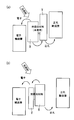
- the light absorbing material in the present embodiment has a structure of the following formula (1). This light-absorbing material imparts an excellent photoelectric conversion function to the photoelectric conversion element.
- X is a site that is excited by absorbing light (hereinafter referred to as a light absorption site), Y is a radical in at least one of an oxidized state or a reduced state, and a site that can be repeatedly redox (hereinafter referred to as a radical). (Referred to as site).
- This light-absorbing material has a structure in which an organic dye is bonded to a site that generates a radical in at least one of a photochemical or electrochemical oxidation reaction or reduction reaction.
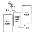
- the radical site Y is an electron donor for the light absorption site X or an electron acceptor for the light absorption site X.
- the radical site Y promotes the oxidation or reduction reaction of the light-absorbing site X that occurs in the photoelectric conversion process of the light-absorbing material.
- the charge moves between the radical site Y and the light absorption site X, and the light absorption part X is reduced or oxidized, and the radical site Y is oxidized or reduced.
- the holes move from the oxidized radical site Y to the charge transport layer and the like, whereby the radical site Y is reduced, and the electrons move from the reduced light absorption site X to the electron transport layer and the like.
- the light absorption site X is oxidized.
- the radical site Y is an electron acceptor for the light absorption site X
- the light absorption site X is excited by absorbing light, the charge is transferred between the radical site Y and the light absorption site X to absorb light.
- Part X is oxidized and radical site Y is reduced.
- the radical site Y is not an active part that generates radicals but a site that can be a stable radical.
- the state where the spin concentration per molecule of the light-absorbing material is 1 or more continues in an equilibrium state for 1 second or more. Is preferred. In this case, a stable redox reaction occurs under conditions where light is continuously irradiated.
- the oxidized or reduced radical site Y returns to the original state by the hole transport layer or the electron transport layer.
- the upper limit of the spin concentration per molecule of the light-absorbing material is preferably 10,000, but is not limited thereto.
- excited electrons or holes generated by one light absorption site X absorbing light move to one radical site Y, and this radical site Y is reduced or oxidized.
- the light absorbing material is a material having a relatively large molecular weight such as an oligomer structure or a polymer structure and the spin concentration per molecule of the light absorbing material is 2 or more, it is reduced or oxidized by the above process.
- electrons or holes may move to another radical site Y in the same molecule by a self-electron exchange reaction. This is a phenomenon called so-called charge hopping transport. If the spin concentration is as described above, the charges move efficiently.
- the radical spin concentration is quantified by an electron spin resonance apparatus.
- the radical site Y that serves as an electron donor for the light absorption site X will be described.
- the holes move quickly from the light absorption site X to the radical site Y, so that quick charge separation occurs.
- radical site Y that can be an electron donor for the light absorption site X
- examples of the chemical structure of the radical site Y that can be an electron donor for the light absorption site X include the radical structure described in Japanese Patent No. 3687736 and Japanese Patent Application Laid-Open No. 2003-100360.
- the radical site Y that serves as an electron donor for the light-absorbing site X preferably has a nitroxide radical (—NO—). In this case, the photoexcited light absorption site X is reduced by the radical site Y at a higher speed.
- radical site Y having a nitroxide radical include the structures shown in the following structural formulas (2) to (5).
- A represents a binding site interposed between a radical site Y and a light absorption site described later, and A may not exist.
- the radical site Y may contain a hydrazyl radical. Also in this case, the photoexcited light absorption site X is reduced by the radical site Y at a higher speed.
- the radical site Y that can be an electron donor for the light absorption site X is derived from, for example, the compounds shown in the following [Chemical 5] and [Chemical 6].
- the radical site Y that can be an electron donor for the light absorption site X is a radical in the ground state, it needs to be stabilized thermodynamically or kinetically.
- stabilization is achieved by a resonance effect, for example, and in the latter case, stabilization is achieved by a steric effect by, for example, a tetramethyl structure.
- the radical site Y that serves as an electron acceptor for the light absorption site X will be described.
- electrons move quickly from the light absorption site X to the radical site Y, so that quick charge separation occurs.
- the radical site Y that can be an electron acceptor for the light absorption site X includes any of a bipyridinium group, a bipyridinium group having a substituent, a galvinoxyl radical group, and a galvinoxyl radical group having a substituent.
- the radical site Y preferably has a structure represented by the following [Chemical Formula 7] or a structure represented by the following [Chemical Formula 8] as at least a part of its chemical structure.
- the chemical structure of the light-absorbing site X includes the book “Latest Solar Cell Overview” (Information Technology Association) and “FPD / DSSC / Optical memory and the latest technology and material development of functional dyes” (NTS Corporation). ] Ruthenium metal complexes (Ru metal complexes) such as [Ru (4,4′-dicarboxyl-2,2′-bipyridine) 2- (NCS) 2 ] and porphyrin metal complexes; Organic dyes such as indoline-based, coumarin-based, merocyanine-based, and squalinium-based pigments; phthalocyanine-based, dioxazine-based, azo-based (soluble azo-based / insoluble azo-based) pigments, selenium-based, and cynadoline-based pigments; cadmium sulfide, sulfide Examples thereof include semiconductor ultrafine particles such as sulfide semiconductors such as lead and silver sulfide.
- the light absorption site X has a molecular structure of a dye
- the light absorption site X has a so-called donor-acceptor type molecular structure
- charges are separated in the light absorption site X during photoexcitation. It is effective in improving the open circuit voltage and short circuit current of the element.
- the light absorption site X has a chemical structure of an associative dye
- a photoelectric conversion element having excellent characteristics (luminescence efficiency) about 5 times as compared with the case where a conventional ruthenium complex is used can be obtained.
- the light absorption site X has a dye structure as disclosed in Japanese Patent No. 4080288, a radical side reaction is suppressed at the time of light irradiation in a photoelectric conversion element including a light absorption material. The effect (light stabilization effect) is expected.
- the light absorption site X preferably has a structure represented by any of the following general formulas (A) to (C).
- the light absorption site X efficiently absorbs light and photoexcites, so that the redox reaction between the light absorption site X and the radical portion Y proceeds rapidly.
- R ′ is hydrogen, carboxyl group, sulfonyl group, phenyl group, carboxyphenyl group, sulfophenyl group, or pyridinium group, and at least one R ′ is substituted with Y.
- M represents a metal atom.
- M is preferably a transition metal atom such as Zn.
- X 1 and X 2 are each independently a group containing at least one of an alkyl group, an alkenyl group, an aralkyl group, an aryl group, and a heterocyclic ring, and each may have a substituent.
- the radical site Y is bonded to either X 1 or X 2 .
- R ′ is hydrogen, carboxyl group, sulfonyl group, phenyl group, carboxyphenyl group, sulfophenyl group, or pyridinium group, and at least one R ′ is substituted with Y.
- the light absorption site X having a structure shown in the general formula (A) is derived from, for example, a compound shown in the following [Chemical Formula 12].
- the light absorption site X having a structure shown in the general formula (C) is derived from, for example, a compound shown in the following [Chemical Formula 13].
- n is an integer of 0 to 10. In the formula (8), n is an integer of 1 to 20.
- the absorption wavelength range is widened.
- the short circuit current of the conversion element is further improved.
- the light absorbing material may have a binding site A interposed between the radical site Y and the light absorbing site X.
- the binding site A is not essential, and the light absorption site X and the radical site Y may be directly bonded.
- binding site A examples include various divalent groups such as methylene, ethylene, propane-1,3-dienyl, ethylidene, propane-2,2-diyl, alkanediyl, benzylidene, propylene, i-propylene, butylene.
- T-butylene octylene, 2-ethylhexylene, 2-methoxyethylene, benzylene, trifluoromethylene, cyanomethylene, ethoxycarbonylmethylene, propoxyethylene, 3- (1-octylpyridinium-4-yl) propylene, 3- (1-butyl-3-methylpyridinium-4-yl) groups of divalent saturated hydrocarbons which may be substituted, linear or branched, such as propylene; vinylidene, propene-1,3- Groups of divalent unsaturated hydrocarbons such as diyl, but-1-ene-1,4-diyl; Groups of divalent cyclic hydrocarbons such as rhohexanediyl, cyclohexenediyl, cyclohexadienediyl, phenylene, naphthalene, biphenylene; oxalyl, malonyl, succinyl, glutanyl,
- the light absorption part X is an organic material
- the light absorption material has a structure in which the light absorption part X and the radical part Y are ⁇ -conjugated
- the light absorption region of the light absorption material is on the long wavelength side. It is preferable from the viewpoint of movement.
- the photoelectric conversion element includes an electron transport layer or a hole transport layer
- the light absorbing material is bonded to at least one of the electron transport layer and the hole transport layer
- the charge transfer efficiency is further improved.
- the bonding mode between the light absorbing material and the electron transporting layer or the hole transporting layer is not particularly limited.
- the electron transporting layer formed from an oxide semiconductor and the light absorbing material are bonded, the bonding force with the electron transporting layer is reduced.
- a light absorbing material having a group such as a carboxyl group, a sulfo group, or a phosphone group is used. By combining these groups with the electron transport layer, the light absorbing material and the electron transport layer are firmly bonded.
- the electron transport layer formed from the organic semiconductor and the amount of the light absorbing agent are bonded, for example, a light absorbing material having a functional group having high adsorptivity to the organic semiconductor or a functional group causing a chemical bond with the organic semiconductor is used. .
- a light-absorbing material having a radical part Y that serves as an electron donor for the light-absorbing site X is produced, for example, as follows. 4 to 22, “on” means “one night” (overnight), and “rt” means “room temperature” (room temperature).
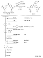
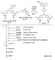
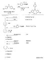
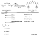
- the light absorbing material represented by the structural formula (6) is manufactured by the steps shown in [Chemical Formula 22], [Chemical Formula 23] and FIGS.
- the compound represented by the structural formula (6) -1 and diethyl ether are mixed with stirring at ⁇ 78 ° C., and tertiary butyl lithium is added thereto. Stir and mix at 78 ° C. for 2 hours, followed by 1 hour at room temperature. 2-Methyl-2-nitrosopropane was added to the resulting mixture, followed by stirring and mixing at ⁇ 78 ° C. for 2 hours, followed by stirring and mixing at room temperature for 10 hours, whereby structural formula (6) — 2 is obtained (yield 40-50%).
- the compound represented by the structural formula (6) -3 and tetrahydrofuran are stirred and mixed at ⁇ 78 ° C., and then the compound represented by the structural formula (6) -a is added.
- the mixture is stirred for 2 hours at ⁇ 78 ° C., and then stirred and mixed for 10 hours at room temperature.
- a saturated solution of monochloroamine, diethyl ether and tetrahydrofuran, and a 10% aqueous hydrochloric acid solution are sequentially added to the resulting mixture, and the mixture is stirred and mixed at room temperature for 10 minutes, whereby the compound represented by the structural formula (6) -4 is obtained. Is obtained (yield 50-60%).
- the compound represented by the structural formula (6) -4, the compound represented by the structural formula (6) -b, tris (dibenzylideneacetone) dipalladium (0), Sodium tertiary riboxide, tritertiarybutylphosphine and toluene are mixed and refluxed overnight to obtain the compound represented by the structural formula (6) -5 (yield 50-60%).
- the compound represented by the structural formula (6) -6, tetra-n-butylammonium fluoride (TBAF), and tetrahydrofuran are stirred at room temperature for 5 hours in an argon atmosphere. After mixing, silver oxide is added and further stirred and mixed at room temperature for 2 hours under an argon atmosphere. As a result, a compound represented by the structural formula (6) is obtained (yield 95-100%).
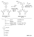
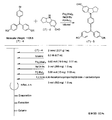
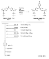
- the light absorbing material represented by the structural formula (7) is manufactured by the steps shown in [Chemical 28], [Chemical 29] and FIGS.
- the compound represented by the structural formula (7) -3 and tetrahydrofuran are stirred and mixed at ⁇ 78 ° C.
- the compound represented by the structural formula (7) -c is added to the mixture thus obtained, mixed at ⁇ 78 ° C. for 2 hours, and then stirred and mixed at room temperature for 10 hours. Further, a saturated solution of monochloroamine, diethyl ether and tetrahydrofuran, and a 10% aqueous hydrochloric acid solution are sequentially added to this mixture, followed by stirring and mixing at room temperature for 10 minutes, whereby a compound represented by the following structural formula (7) -4 is obtained. Is obtained (yield 50-60%).
- the compound represented by the structural formula (7) -4, the compound represented by the structural formula (7) -d, tris (dibenzylideneacetone) dipalladium (0), Sodium tertiary riboxide, tritertiarybutylphosphine, and toluene are mixed and refluxed overnight to obtain a compound represented by the following structural formula (7) -5 (yield: 50-60%) .
- tetra-n-butylammonium fluoride represented by the structural formula (7) -6 and tetrahydrofuran are stirred and mixed at room temperature in an argon atmosphere for 5 hours.
- Silver oxide is further added to the resulting mixture, and the mixture is stirred and mixed at room temperature for 2 hours under an argon atmosphere.
- a compound represented by the structural formula (7) is obtained (yield 95-100%).
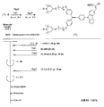
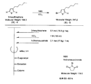
- the light absorbing material represented by the structural formula (8) is manufactured by the steps shown in [Chemical 30] to [Chemical 33] and FIGS.
- the compound represented by the structural formula (8) -1 and diethyl ether are stirred and mixed at ⁇ 78 ° C.
- Tertiary butyllithium is added to the resulting mixture and stirred and mixed at ⁇ 78 ° C. for 2 hours, followed by stirring and mixing at room temperature for 1 hour.
- 2-methyl-2-nitrosopropane was added to this mixture, and the mixture was stirred and mixed at ⁇ 78 ° C. for 2 hours, followed by stirring and mixing at room temperature for 1 hour, thereby showing the structural formula (8) -2. Is obtained (yield 40-50%).
- the compound represented by the structural formula (8) -4, carbon tetrachloride, and N-bromosuccinimide are stirred and mixed at room temperature for 5 hours, whereby the structural formula (8) A compound represented by ⁇ 5 is obtained (yield 50-60%).
- the compound represented by the structural formula (8) -5 and dimethyl ether are stirred and mixed at ⁇ 78 ° C.
- Tertiary butyllithium is added to the resulting mixture, followed by stirring and mixing at ⁇ 78 ° C. for 2 hours, followed by stirring and mixing at room temperature for 1 hour.
- triisopropyl borate is added to this mixture, followed by stirring and mixing at ⁇ 78 ° C. for 2 hours, followed by stirring and mixing at room temperature for 10 hours to obtain a compound represented by the structural formula (8) -B. (Yield 40-50%).
- the compound represented by the structural formula (8) -A, the compound represented by the structural formula (8) -B, toluene, sodium tertiary carboxide, tetra ( (Triphenylphosphinato) palladium is mixed and refluxed overnight under an argon atmosphere to obtain the compound represented by the structural formula (8) -C.
- the compound represented by the structural formula (8) -C 2-cyanoacetic acid, acetonitrile (AN), piperidine, and tetra (triphenylphosphinato) palladium are mixed.
- the compound represented by the structural formula (8) -D is obtained (yield 80 to 90%).
- the compound represented by the structural formula (8) -D, tetra-n-butylammonium fluoride, and tetrahydrofuran are stirred and mixed at room temperature in an argon atmosphere for 5 hours.
- Silver oxide is added to the resulting mixture and stirred and mixed at room temperature for 2 hours under an argon atmosphere.
- a compound represented by the structural formula (8) is obtained (yield 95-100%).
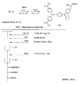
- the compound represented by the structural formula (11) is a fine particle called a quantum dot produced by a method described in “Chemistry Letters” 2007, Vol. 36, No. 6, page 712, for example, “Journal of Molecular. Catalysis A: Chemical ”, 1995, Vol. 101, p. 45, manufactured by binding to a stable free radical by a method as described.
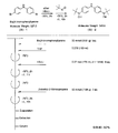
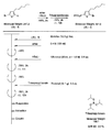
- a light-absorbing material having a radical part Y that serves as an electron acceptor for the light-absorbing site X is produced, for example, as follows.
- the light absorbing material represented by the structural formula (14) is manufactured by a chemical reaction represented by the following [Chemical Formula 34], for example.
- a compound represented by the structural formula (14) -1 and a Dl31 dye are added to a tetrahydrofuran (THF) / ethanol mixed solvent, and an ester condensing agent (4- (4,6-dimethoxy-1,3,5) is added.
- an ester condensing agent (4- (4,6-dimethoxy-1,3,5) is added.
- -Triazin-2-yl) -4-methylmorpholinium chloride; DMT-MM) and a base (triethylamine; TEA) are added.
- a compound represented by the structural formula (14) -2 is produced (yield 70%).
- the compound represented by the structural formula (14) -2 is added to ethanol, and an excessive amount of iodomethane is further added.
- the solution thus obtained is left at 60 ° C. overnight, then washed with water and the product is reprecipitated in diethyl ether. Thereby, the reddish brown solid of the light absorption material shown by Structural formula (14) is obtained (yield 65%).
- the light absorbing material represented by the structural formula (14) is soluble in chloroform, acetonitrile, and methanol and insoluble in water.
- the light absorbing material represented by the structural formula (14) is identified by 1H-NMR and FAB-Mass.
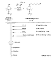
- the light absorbing material represented by the structural formula (15) is manufactured by a chemical reaction represented by the following [Chemical Formula 35].
- cyanoacetic acid is dissolved in acetonitrile, and 1-carbonyldiimidazole is further added to activate the carboxyl group.
- a viologen derivative represented by the structural formula (14) -1 synthesized by the reaction represented by [Chemical Formula 30] is added to form an amide bond, and the compound represented by the structural formula (15) -1 Is obtained. Formation of the compound represented by the structural formula (15) -1 is confirmed by FAB-Mass.
- the compound represented by the structural formula (15) -1 is added to ethanol, and further, a base and a D131 dye are added, whereby the compound represented by the structural formula (15) -1 and the D131 dye are condensed.
- a light absorbing material represented by the structural formula (15) is obtained.
- the light absorbing material represented by the structural formula (16) is manufactured by a chemical reaction represented by the following [Chemical Formula 36].
- the compound represented by the structural formula (16) -2 is added to methanol, and a condensing agent (DMT-MM) and a base (triethylamine (TEA)) are further added to the resulting solution.
- a compound represented by the structural formula (16) -3 is obtained (yield 92%).
- the compound represented by Structural Formula (16) -3 is added to ethanol, and an excess amount of iodomethane is further added to the resulting solution.
- the light absorbing material represented by the structural formula (17) is manufactured by a chemical reaction represented by the following [Chemical Formula 37].
- a compound represented by the structural formula (17) -1 is formed by a coupling reaction by lithiation of 4- (methoxycarbonyl) phenylboronic acid. Subsequently, PdCl 2 (PPh 3 ) 2 , triethylamine, 4,4,5,5-tetramethyl, and 1,3,2-dioxaborolane are added to the compound represented by the structural formula (17) -1, thereby obtaining The resulting mixture is stirred for 5 hours at 80 ° C. in toluene under an inert atmosphere. Next, liquid separation and HPLC purification of this mixture gives an amber powder of the compound represented by the structural formula (17) -2.
- the compound represented by the structural formula (17) -2 and MD-22 are added in a benzene / water mixed solvent, and Pd (PPh 3 ) 4 and K 2 CO 3 are further added to the resulting solution.
- Pd (PPh 3 ) 4 and K 2 CO 3 are further added to the resulting solution.
- this solution is allowed to stand at 50 ° C. for 12 hours, the reaction proceeds (Suzuki coupling).
- reddish-amber powder of the compound represented by the structural formula (17) -3 is obtained by separation and HPLC purification of this solution.
- the light absorbing material is applied to a photoelectric conversion element such as a dye-sensitized type such as a light emitting element or a solar cell.
- the photoelectric conversion element is composed of, for example, a charge transport material or a conductive substrate for transporting holes and electrons.
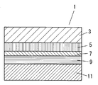
- FIG. 1 is a cross-sectional view showing an example of a dye-sensitized solar cell 1 among photoelectric conversion elements.
- this dye-sensitized solar cell 1 a layer (electron transport layer) formed from the electron transport material 5 between the first substrate electrode 3 and the second substrate electrode 11 disposed so as to face each other.
- a layer formed from the light absorbing material 7 and a layer formed from the charge transport material 9 (hole transport layer) are laminated.
- At least one of the first substrate electrode 3 and the second substrate electrode 11 has translucency.
- the first substrate electrode 3 and the second substrate electrode 11 have conductivity for extracting charges to the outside.
- the translucent substrate electrode may be transparent or opaque, but is particularly preferably transparent.
- the second substrate electrode 11 is formed from a metal foil, the first substrate electrode 3 is preferably formed from a light-transmitting material.
- the first substrate electrode 3 may include a base material formed of, for example, glass or a film.
- the first substrate electrode 3 includes, for example, a conductive layer laminated on a base material.
- the conductive layer is laminated on the surface of the substrate facing the electron transport material 5.
- the conductive layer is made of, for example, a metal such as indium; carbon; a conductive metal oxide such as indium-tin composite oxide, tin oxide doped with antimony or tin oxide doped with fluorine; It is formed from things.
- the first substrate electrode 3 includes a layer formed from the above compound and a layer formed from silicon oxide, tin oxide, titanium oxide, zirconium oxide, aluminum oxide, or the like that coats the layer. Good.
- the first substrate electrode 3 is formed by a dry process such as vapor deposition or sputtering, or a wet process such as dipping, spray pyrolysis, or CVD.
- the first substrate electrode 3 may include a film formed of a metal foil such as titanium, nickel, zinc, and stainless steel.
- the second substrate electrode 11 functions as a negative electrode of the photoelectric conversion element.
- the second substrate electrode 11 is made of only metal, for example.
- the second substrate electrode 11 may include a film and a conductive layer laminated on the film. This conductive layer is in contact with the layer formed from the charge transport material 9.
- the conductive layer in the second substrate electrode 11 is formed of, for example, the same material as the conductive layer in the first substrate electrode 3.
- the conductive layer in the second substrate electrode 11 is, for example, a metal such as platinum, gold, silver, copper, aluminum, rhodium, or indium; a carbon material such as graphite, carbon nanotube, or carbon carrying platinum; an indium-tin composite oxide; It is formed from a conductive metal oxide such as tin oxide doped with antimony or tin oxide doped with fluorine; a conductive polymer such as polyethylenedioxythiophene, polypyrrole or polyaniline.
- the second substrate electrode 11 is preferably formed from platinum, graphite, polyethylenedioxythiophene, or the like.
- the surface resistances of the first substrate electrode 3 and the second substrate electrode 11 are preferably 200 ⁇ / ⁇ or less, and more preferably 50 ⁇ / ⁇ or less.
- the lower limit of the surface resistance range of the first substrate electrode 3 and the second substrate electrode 11 is not particularly limited, but is usually 0.1 ⁇ / ⁇ .
- the light transmittance of the substrate electrode having a high light transmittance is preferably 50% or more, and more preferably 80% or more.
- the thickness of the conductive layer in the first substrate electrode 3 and the second substrate electrode 11 is preferably in the range of 0.1 to 10 ⁇ m. Within this range, a conductive layer having a uniform thickness can be easily formed, and the light transmittance of the conductive layer can be maintained.
- the electron transport material 5 is not particularly limited as long as it is a material using electrons as carriers.
- semiconductor materials used as the electron transport material 5 Cd, Zn, In, Pb, Mo, W, Sb, Bi, Cu, Hg, Ti, Ag, Mn, Fe, V, Sn, Zr, Sr, Ga, Metal element oxides such as Si and Cr; metal oxides having a perovskite structure such as SrTiO 3 and CaTiO 3 ; CdS, ZnS, In 2 S 3 , PbS, Mo 2 S, WS 2 , Sb 2 S 3 , Bi Sulfides such as 2 S 3 , ZnCdS 2 , Cu 2 S; metal chalcogenides such as CdSe, In 2 Se 3 , WSe 2 , HgS, PbSe, CdTe; GaAs, Si, Se, Cd 2 P 3 , Zn 2 P 3 , InP, AgBr, PbI 2 , HgI
- the electron transport material 5 may be a composite containing at least one selected from the semiconductor materials as described above.
- Such composites for example, CdS / TiO 2, CdS / AgI, Ag 2 S / AgI, CdS / ZnO, CdS / HgS, CdS / PbS, ZnO / ZnS, ZnO / ZnSe, CdS / HgS, CdS / CdSe, CdS / Te, CdSe / Te, ZnS / CdSe, ZnSe / CdSe, CdS / ZnS, TiO 2 / Cd 3 P 2 , CdS / CdSe / CdZnS, CdS / HgS / CdS, and the like.
- the electron transport material 5 may be a conductive polymer such as polythiophene or polyaniline, a redox polymer having a redox side chain, C60, or the like that can become an n-type semiconductor by doping.
- the electron transport material 5 may be a polyradical compound which is an n-type semiconductor and exhibits stable oxidation-reduction behavior as disclosed in JP-A-2008-280400.
- the density of molecules of the light absorbing material relative to the projected area of the photoelectric conversion element depends on the light absorption efficiency of the light absorbing material 7 from the viewpoint of output characteristics.
- the range of ⁇ 10 ⁇ 8 to 1 ⁇ 10 ⁇ 6 mol / cm 2 is preferable.
- the density of the light absorbing material 7 is larger than the above range, the amount of the light absorbing material 7 with respect to incident light is too large, so that the amount of the light absorbing material 7 that does not act increases.
- the density of the light absorbing material 7 is smaller than the above range, a sufficient amount of light is not absorbed by the light absorbing material 7.
- the entire photoelectric conversion element is a so-called see-through type element having translucency
- the density and absolute amount of the light-absorbing material 7 are reduced according to the light transmittance desired for the photoelectric conversion element. Also good.
- the layer formed from the electron transport material 5 is porous and the ratio of the effective area to the projected area is 1 or more, the photoelectric conversion efficiency of the photoelectric conversion element is particularly improved.
- the upper limit of the ratio of the effective area to the projected area of the layer formed from the electron transport material 5 is not particularly limited, but is preferably 1 million or less.
- Examples of the charge transport material (hole transport material) 9 include substances that generate redox pairs. As such a charge transport material 9, iodine (I ⁇ / I 3 ⁇ ) is generally used in many cases, but is not limited thereto.
- the charge transport material 9 may be a radical compound that is stably oxidized and reduced as described in JP-A-2003-100360.
- the radical site Y in the light-absorbing material 7 is an electron donor because the reduction reaction of the oxidized radical site Y is promoted and the oxidized radical site Y is rapidly reduced.
- the charge transport material 9 may be an electrolyte solution.
- the solvent used for dissolving the electrolyte is preferably a compound that can dissolve the redox constituent and has excellent ion conductivity.
- the solvent may be either an aqueous solvent or an organic solvent, but an organic solvent is preferable in order to stabilize the oxidation-reduction component in the electrolyte solution.
- organic solvent examples include carbonate compounds such as dimethyl carbonate, diethyl carbonate, methyl ethyl carbonate, ethylene carbonate, and propylene carbonate; ester compounds such as methyl acetate, methyl propionate, and ⁇ -butyrolactone; diethyl ether, 1,2-dimethoxy Ether compounds such as ethane, 1,3-dioxosilane, tetrahydrofuran, 2-methyl-tetrahydrofuran; heterocyclic compounds such as 3-methyl-2-oxazozirinone, 2-methylpyrrolidone; nitrile compounds such as acetonitrile, methoxyacetonitrile, propionitrile Aprotic polar compounds such as sulfolane, dimethyl sulfoxide and dimethylformamide; These solvents may be used alone or in combination of two or more.
- carbonate compounds such as dimethyl carbonate, diethyl carbonate, methyl ethyl carbonate, ethylene carbonate,
- carbonate compounds such as ethylene carbonate and propylene carbonate
- heterocyclic compounds such as ⁇ -butyrolactone, 3-methyl-2-oxazodilinone and 2-methylpyrrolidone
- acetonitrile, methoxyacetonitrile, propionitrile, 3-methoxypropyl Nitrile compounds such as pionitrile and valeric nitrile
- polyol compounds such as ethylene glycol, polyethylene glycol and polyethylene are preferably used.
- the charge transport material 9 may be gelled by containing a polymer matrix such as an oil gel-based or polyvinylidene fluoride-based polymer compound, a liquid crystal gel, a low molecule such as an amino acid derivative, or inorganic particles such as silica particles. .
- a polymer matrix such as an oil gel-based or polyvinylidene fluoride-based polymer compound, a liquid crystal gel, a low molecule such as an amino acid derivative, or inorganic particles such as silica particles.
- the charge transporting material 9 may be a conductive polymer such as polythiophene or polyaniline, a polymer having a side chain that can be easily oxidized or reduced, or the like if it can be a p-type semiconductor by doping. In this case, since the layer formed of the charge transport material 9 is in a solid or gel state, liquid leakage is suppressed, and thus the photoelectric conversion efficiency of the photoelectric conversion element is maintained high over a long period of time.
- the redox potential of the radical site Y and the redox potential of the hole transport material or the electron transport material are adjusted so that charge separation proceeds smoothly.
- the radical site Y in the light absorbing material 7 is an electron donor and the redox potential of the hole transport material 9 is lower than the redox potential of the radical site Y, the charge separation in the light absorbing material 7 is performed. Progresses more smoothly.
- the structure of the radical site Y is a structure as exemplified in the present specification, the potential is adjusted by introducing a functional group into the radical site Y. This can be achieved relatively easily by changing the molecular structure.
- the radical site Y promotes the oxidation or reduction reaction of the light absorption site X, and thus high-speed charge separation. And recombination of charges is suppressed. For this reason, the photoelectric conversion of a photoelectric conversion element becomes high.
- the excited light is generated in the photoelectric conversion process caused by the light absorption site X absorbing light.
- the reduction reaction of the light absorption site X is promoted.
- the radical site Y is oxidized.
- the radical site Y is reduced and holes move from the radical site Y to the hole transport layer.
- the electrons move from the reduced light absorption site X to the electron transport layer, the light absorption site X is oxidized.
- FIG. 3 shows a conventional example.
- the light absorbing material can exhibit the same action as HALS (light stabilizer).
- HALS light stabilizer
- the compound represented by the structural formula (6) -2 (10 mmol (3.56 g) 1 eq), DMF (0.7 M (14.3 ml)) and imidazole (30 mmol (2.10 g) 3 eq) and tertiary butyldimethylsilyl chloride (12.5 mol (1.88 g) 1.25 eq) were stirred and mixed at room temperature for 10 hours to obtain a compound represented by the structural formula (6) -3 ( Yield 80-90%).
- the compound represented by the structural formula (6) -3 (5 mmol (2.92 g) 1 eq) and tetrahydrofuran (0.3 M (16.7 ml)) were stirred and mixed at ⁇ 78 ° C.
- the compound represented by the structural formula (6) -a (15 mol (4.11 g) 1.5 eq) was added to the resulting solution, and the mixture was stirred and mixed at ⁇ 78 ° C. for 2 hours and at room temperature for 10 hours.
- the compound represented by the structural formula (6) -6 (1 mmol (911 mg) 1 eq), TBAF (20 mmol (5.23 g) 20 eq) and THF (50 mM (20 ml)) were added in an argon atmosphere. Under stirring at room temperature for 5 hours, silver oxide (10 mol (2.31 g) 10 eq) was added to the resulting solution and stirred and mixed at room temperature for 2 hours under an argon atmosphere. As a result, a compound represented by the structural formula (6) was obtained (yield 95-100%).
- the compound represented by the structural formula (7) -3 (5 mmol (4.77 g) 1 eq) and tetrahydrofuran (0.3 M (16.7 ml)) were stirred and mixed at ⁇ 78 ° C. Further, the compound represented by the structural formula (7) -c (15 mol (4.11 g) 1.5 eq) was added to the obtained solution and mixed at ⁇ 78 ° C. for 2 hours, and then this solution was stirred at room temperature for 10 hours.
- the compound represented by the structural formula (8) -2 (10 mmol (5.72 g) 1 eq), DMF (0.7 M (14.3 ml)) and imidazole (30 mmol (2.10 g) 3 eq) and tertiary butyldimethylsilyl chloride (12.5 mol (1.88 g) 1.25 eq) were stirred and mixed at room temperature for 10 hours to obtain a compound represented by the structural formula (8) -3 ( Yield 80-90%).
- the compound represented by the structural formula (8) -3 (10 mmol (5.72 g) 1 eq), toluene (0.7 M (14.3 ml)) and sodium tertiary oxide (12. 5 mol (1.20 g) 1.25 eq), copper iodide (1 mmol (0.19 g) 0.1 eq) and piperidine (1.0 mol (85 mg) 0.01 eq) were stirred and mixed, and the resulting solution was mixed with argon. By refluxing in an atmosphere for 5 hours, a compound represented by the structural formula (8) -A was obtained (yield: 50 to 60%).
- the compound represented by the structural formula (8) -4 (0.1 mol (16.8 g) 1 eq), carbon tetrachloride (1M (100 ml)) and N-bromosuccinimide (0. 1 mol (17.8 g) 1 eq) was stirred and mixed at room temperature for 3 hours to obtain a compound represented by the structural formula (8) -5 (yield: 50 to 60%).
- the compound represented by the structural formula (8) -5 50 mmol (12.3 g) 1 eq) and dimethyl ether (0.4 M (125 ml)) were stirred and mixed at ⁇ 78 ° C.
- triisopropyl borate 75 mmol (14.1 g) 1.5 eq
- a compound represented by the formula (8) -B was obtained (yield 40-50%).
- the compound represented by the structural formula (8) -C (1 mmol (0.814 g) 1 eq), 2-cyanoacetic acid (1.2 mmol (0.102 g) 1.2 eq) and AN (0.3 M (6.7 ml)), piperidine (0.03 mmol (2.5 mg) 0.03 eq) and tetra (triphenylphosphinato) palladium (0.01 mmol (12.6 mg) 0.01 eq) were mixed.
- the resulting solution was refluxed for 5 hours under an argon atmosphere to obtain the compound represented by the structural formula (8) -D (yield 80 to 90%).
- the compound represented by the structural formula (8) -D (1 mmol (909 mg) 1 eq), TBAF (20 mmol (5.23 g) 20 eq), and THF (50 mM (20 ml)) are mixed with argon.
- the mixture was stirred and mixed at room temperature for 5 hours under an atmosphere, silver oxide (10 mol (2.31 g) 10 eq) was added to the resulting solution, and the mixture was stirred and mixed at room temperature for 2 hours under an argon atmosphere.
- a compound represented by the structural formula (8) was obtained (yield 95-100%).
- a screen printing paste was obtained by dispersing high-purity titanium oxide powder having an average primary particle diameter of 20 nm in ethyl cellulose.
- a first substrate electrode was produced by forming a 10 nm thick titanium oxide film by sputtering on a 1 mm thick conductive glass substrate (fluorine-doped tin oxide, surface resistance 100 ⁇ / ⁇ ). After applying the screen printing paste on the first substrate electrode, it was dried to form a dry film. This dried film was baked in air at 500 ° C. for 30 minutes. Thereby, a porous titanium oxide film having a thickness of 1.5 ⁇ m was formed on the first substrate electrode.
- the porous titanium oxide film was heated at 70 ° C. for 30 minutes, and then this porous titanium oxide film was used. The membrane was rinsed with distilled water and then air dried. As a result, an electron transport layer was formed on the first substrate electrode.
- Each dimethylformamide solution was prepared. The concentration of the light absorbing material in each solution was 0.2 mM.
- the electron transport layer was immersed in a dimethylformamide solution containing the light absorbing material together with the first substrate electrode, and in this state, the electron transport layer was allowed to stand at room temperature in the dark for 24 hours. Subsequently, the electron transport layer was washed with a solvent.
- a platinum film was formed on the surface of a conductive glass substrate (manufactured by Nippon Sheet Glass, fluorine-doped SnO 2 , surface resistance: 10 ⁇ / ⁇ ) by thermal reduction of chloroplatinic acid to obtain a second substrate electrode.
- the first substrate electrode and the second substrate electrode were opposed to each other so that the electron transport layer was disposed between them. Between this first substrate electrode and the second substrate electrode, a sealing material (hot melt adhesive, trade name Binnel made by Mitsui DuPont Polychemical Co., Ltd.) is removed except for one side of the electron transport layer. Arranged so as to surround. In this state, the first substrate electrode and the second substrate electrode were pressed while being heated, so that both were bonded via a sealing material.
- a sealing material hot melt adhesive, trade name Binnel made by Mitsui DuPont Polychemical Co., Ltd.
- An electrolyte solution was prepared by dissolving at a concentration of 025 mol / dm 3 .
- the electrolyte solution was injected between the first substrate electrode and the second substrate electrode through a gap that was not blocked by the sealing material. Subsequently, the gap that was not blocked by the sealing material was blocked with an ultraviolet curable resin. Thereby, a photoelectric conversion element having a light receiving area of 1 cm 2 was obtained.
- Example 4 A first substrate electrode was obtained by forming a fluorine-doped SnO 2 layer on a 1 mm thick conductive glass substrate (manufactured by Asahi Glass Co., Ltd., surface resistance 10 ⁇ / ⁇ ).
- a platinum plate was prepared as the second substrate electrode.
- the second substrate electrode and the first substrate electrode were opposed to each other so that a film of a light absorbing material was disposed between them, and the space between them was surrounded by a sealing material. Subsequently, the first substrate electrode and the second substrate electrode were pressurized while being heated, so that both were bonded together via a sealing material.
- the open-circuit voltage of this photoelectric conversion element under light irradiation was 480 mV, and when the light was cut off, the output voltage gradually converged to 0 mV. When the light was irradiated again, the open circuit voltage converged to 480 mV. This light response behavior was repeatedly and stably expressed.
- Example 7 Instead of the light absorbing material represented by the structural formula (14), the light absorbing material represented by the structural formula (15) in Example 5, the light absorbing material represented by the structural formula (16) in Example 6, and Example 7 Then, the light absorption material shown by Structural formula (17) was used, respectively. Otherwise, a photoelectric conversion element was produced under the same method and conditions as in Example 4.
- the open-circuit voltage of this photoelectric conversion element was measured in the same manner as in Example 4. As a result, it was 430 mV in Example 5, 410 mV in Example 6, and 380 mV in Example 7. A behavior was developed.
- the open circuit voltage of this photoelectric conversion element under light irradiation was 90 mV, and when the light was cut off, the output voltage gradually converged to 0 mV. When light was irradiated again, the open circuit voltage converged to 90 mV. This light response behavior was repeatedly and stably expressed.
- the open-circuit voltage of this photoelectric conversion element under light irradiation was 40 mV, and when the light was cut off, the output voltage gradually converged to 0 mV. Furthermore, when light was irradiated again, the output voltage converged to 40 mV. This light response behavior was repeatedly and stably expressed.
Landscapes
- Chemical & Material Sciences (AREA)
- Organic Chemistry (AREA)
- Engineering & Computer Science (AREA)
- Materials Engineering (AREA)
- Physics & Mathematics (AREA)
- Spectroscopy & Molecular Physics (AREA)
- Chemical Kinetics & Catalysis (AREA)
- Power Engineering (AREA)
- General Chemical & Material Sciences (AREA)
- Electrochemistry (AREA)
- Microelectronics & Electronic Packaging (AREA)
- Photovoltaic Devices (AREA)
- Hybrid Cells (AREA)
Priority Applications (4)
| Application Number | Priority Date | Filing Date | Title |
|---|---|---|---|
| US13/322,048 US8729532B2 (en) | 2009-05-22 | 2010-05-21 | Light-absorbing material and photoelectric conversion element |
| KR1020117030731A KR101366122B1 (ko) | 2009-05-22 | 2010-05-21 | 광흡수 재료 및 광전변환 소자 |
| EP10777838.3A EP2433989B1 (en) | 2009-05-22 | 2010-05-21 | Light-absorbing material and photoelectric conversion element |
| CN201080022143.2A CN102439092B (zh) | 2009-05-22 | 2010-05-21 | 光吸收材料和光电转换元件 |
Applications Claiming Priority (2)
| Application Number | Priority Date | Filing Date | Title |
|---|---|---|---|
| JP2009124522 | 2009-05-22 | ||
| JP2009-124522 | 2009-05-22 |
Publications (1)
| Publication Number | Publication Date |
|---|---|
| WO2010134607A1 true WO2010134607A1 (ja) | 2010-11-25 |
Family
ID=43126284
Family Applications (1)
| Application Number | Title | Priority Date | Filing Date |
|---|---|---|---|
| PCT/JP2010/058662 Ceased WO2010134607A1 (ja) | 2009-05-22 | 2010-05-21 | 光吸収材料及び光電変換素子 |
Country Status (7)
| Country | Link |
|---|---|
| US (1) | US8729532B2 (enExample) |
| EP (1) | EP2433989B1 (enExample) |
| JP (1) | JP5711470B2 (enExample) |
| KR (1) | KR101366122B1 (enExample) |
| CN (1) | CN102439092B (enExample) |
| TW (1) | TW201107457A (enExample) |
| WO (1) | WO2010134607A1 (enExample) |
Cited By (3)
| Publication number | Priority date | Publication date | Assignee | Title |
|---|---|---|---|---|
| WO2012121192A1 (ja) * | 2011-03-10 | 2012-09-13 | パナソニック株式会社 | 光吸収材料及び光電変換素子 |
| JP2015074754A (ja) * | 2013-10-11 | 2015-04-20 | 三菱製紙株式会社 | 有機色素 |
| JP2015097259A (ja) * | 2013-10-11 | 2015-05-21 | パナソニック株式会社 | 光電変換素子 |
Families Citing this family (14)
| Publication number | Priority date | Publication date | Assignee | Title |
|---|---|---|---|---|
| US20130220822A1 (en) * | 2010-11-08 | 2013-08-29 | Bjorn Winther-Jensen | Method and system for catalysis |
| JP5996255B2 (ja) * | 2011-05-09 | 2016-09-21 | 旭化成株式会社 | 光電変換素子及びπ共役型有機ラジカル化合物 |
| JP6010549B2 (ja) | 2011-12-28 | 2016-10-19 | パナソニック株式会社 | 光電気素子及びその製造方法 |
| US9013023B2 (en) | 2011-12-28 | 2015-04-21 | Panasonic Corporation | Photoelectric element having stacked charge-transport layers |
| TWI470776B (zh) | 2011-12-29 | 2015-01-21 | Ind Tech Res Inst | 光偵測陣列結構與光偵測模組 |
| WO2013140181A1 (en) * | 2012-03-22 | 2013-09-26 | The University Of Manchester | Photovoltaic cells |
| EP2926379A4 (en) * | 2012-12-03 | 2016-07-20 | Univ Akron | ORGANIC POLYMER LIGHTING DEVICE WITH BROADBANDING RESPONSE AND INCREASED LIGHTINGABILITY |
| CN104112787B (zh) * | 2014-07-28 | 2016-04-13 | 武汉鑫神光电科技有限公司 | 一种硫化银/钙钛矿体异质结太阳能电池及其制备方法 |
| JP6743812B2 (ja) * | 2015-05-12 | 2020-08-19 | 住友化学株式会社 | 有機光電変換素子 |
| KR20170029371A (ko) | 2015-09-07 | 2017-03-15 | 주식회사 레이언스 | X선 디텍터 |
| WO2017043871A1 (ko) * | 2015-09-07 | 2017-03-16 | 주식회사 레이언스 | X선 디텍터 |
| CN113130769B (zh) * | 2021-04-09 | 2023-10-13 | 东南大学 | 二维层状钙钛矿单晶、宽光谱光电探测器及其制备方法 |
| JP7294601B2 (ja) * | 2021-07-13 | 2023-06-20 | 独立行政法人国立高等専門学校機構 | 光電変換素子の製造方法、光電変換素子、光電変換素子におけるn型半導体層の製造方法 |
| CN115295747B (zh) * | 2022-07-29 | 2025-09-05 | 合肥工业大学 | 基于激基复合物的多量子阱结构改善oled器件性能的方法 |
Citations (9)
| Publication number | Priority date | Publication date | Assignee | Title |
|---|---|---|---|---|
| JP2664194B2 (ja) | 1988-02-12 | 1997-10-15 | エコル ポリテクニク フェデラル ドゥ ローザンヌ | 光電気化学電池・その製法及び使用法 |
| JP2003100360A (ja) | 2001-09-26 | 2003-04-04 | Nec Corp | 光電気化学デバイス |
| JP3687736B2 (ja) | 2000-02-25 | 2005-08-24 | 日本電気株式会社 | 二次電池 |
| JP2007262263A (ja) * | 2006-03-29 | 2007-10-11 | Fujifilm Corp | フタロシアニン化合物 |
| JP4080288B2 (ja) | 2002-09-26 | 2008-04-23 | 三菱製紙株式会社 | 太陽電池用メロシアニン色素 |
| JP2008201912A (ja) * | 2007-02-20 | 2008-09-04 | Fujifilm Corp | 光重合性組成物 |
| JP2008280400A (ja) | 2007-05-09 | 2008-11-20 | Nec Corp | ポリラジカル化合物および電池 |
| JP2009021212A (ja) * | 2007-06-14 | 2009-01-29 | Panasonic Electric Works Co Ltd | 光電変換素子 |
| JP2009081141A (ja) * | 2006-02-02 | 2009-04-16 | Sony Corp | 色素増感型光電変換装置 |
Family Cites Families (3)
| Publication number | Priority date | Publication date | Assignee | Title |
|---|---|---|---|---|
| EP1997855A3 (en) * | 2002-07-29 | 2010-09-08 | Mitsubishi Paper Mills Limited | Organic dye, photoelectric transducing material, semiconductor electrode, and photoelectric transducing device |
| JP2007234580A (ja) * | 2006-02-02 | 2007-09-13 | Sony Corp | 色素増感型光電変換装置 |
| JP5023866B2 (ja) | 2007-07-27 | 2012-09-12 | ソニー株式会社 | 色素増感光電変換素子およびその製造方法ならびに電子機器 |
-
2010
- 2010-05-21 KR KR1020117030731A patent/KR101366122B1/ko active Active
- 2010-05-21 EP EP10777838.3A patent/EP2433989B1/en active Active
- 2010-05-21 JP JP2010117398A patent/JP5711470B2/ja active Active
- 2010-05-21 CN CN201080022143.2A patent/CN102439092B/zh active Active
- 2010-05-21 TW TW099116307A patent/TW201107457A/zh unknown
- 2010-05-21 WO PCT/JP2010/058662 patent/WO2010134607A1/ja not_active Ceased
- 2010-05-21 US US13/322,048 patent/US8729532B2/en active Active
Patent Citations (9)
| Publication number | Priority date | Publication date | Assignee | Title |
|---|---|---|---|---|
| JP2664194B2 (ja) | 1988-02-12 | 1997-10-15 | エコル ポリテクニク フェデラル ドゥ ローザンヌ | 光電気化学電池・その製法及び使用法 |
| JP3687736B2 (ja) | 2000-02-25 | 2005-08-24 | 日本電気株式会社 | 二次電池 |
| JP2003100360A (ja) | 2001-09-26 | 2003-04-04 | Nec Corp | 光電気化学デバイス |
| JP4080288B2 (ja) | 2002-09-26 | 2008-04-23 | 三菱製紙株式会社 | 太陽電池用メロシアニン色素 |
| JP2009081141A (ja) * | 2006-02-02 | 2009-04-16 | Sony Corp | 色素増感型光電変換装置 |
| JP2007262263A (ja) * | 2006-03-29 | 2007-10-11 | Fujifilm Corp | フタロシアニン化合物 |
| JP2008201912A (ja) * | 2007-02-20 | 2008-09-04 | Fujifilm Corp | 光重合性組成物 |
| JP2008280400A (ja) | 2007-05-09 | 2008-11-20 | Nec Corp | ポリラジカル化合物および電池 |
| JP2009021212A (ja) * | 2007-06-14 | 2009-01-29 | Panasonic Electric Works Co Ltd | 光電変換素子 |
Non-Patent Citations (15)
| Title |
|---|
| CHEMISTRY LETTERS, vol. 36, no. 6, 2007, pages 712 |
| J. AM. CHEM. SOC., vol. 117, 1995, pages 2049 - 2057, XP008148190 * |
| J. AM. CHEM. SOC., vol. 122, 2000, pages 11480 - 11487, XP008148189 * |
| J. PHYS. CHEM. A, vol. 106, 2002, pages 4453 - 4467, XP002971037 * |
| JAPANESE JOURNAL OF POLYMER SCIENCE AND TECHNOLOGY, vol. 37, no. 10, 1980, pages 635 - 640, XP008148172 * |
| JOURNAL OF MAGNETIC RESONANCE, vol. 131, 1998, pages 97 - 110, XP004407512 * |
| JOURNAL OF MAGNETIC RESONANCE, vol. 52, 1983, pages 435 - 449, XP023958607 * |
| JOURNAL OF MAGNETIC RESONANCE, vol. 60, 1984, pages 54 - 65, XP023956226 * |
| JOURNAL OF MOLECULAR CATALYSIS A: CHEMICAL, vol. 101, 1995, pages 45 |
| JOURNAL OF MOLECULAR CATALYSIS B: ENZYMATIC, vol. 17, 2002, pages 9 - 21, XP008148170 * |
| JOURNAL OF PHOTOCHEMISTRY AND PHOTOBIOLOGY A: CHEMISTRY, vol. 133, 2000, pages 105 - 114, XP008148191 * |
| MOLECULAR PHYSICS, vol. 100, no. 9, 2002, pages 1459 - 1468, XP008148227 * |
| PHYSICAL CHEMISTRY CHEMICAL PHYSICS, vol. 7, 2005, pages 4114 - 4125, XP008148224 * |
| See also references of EP2433989A4 |
| TETRAHEDRON LETTERS, vol. 47, 2006, pages 5637 - 5640, XP025004598 * |
Cited By (3)
| Publication number | Priority date | Publication date | Assignee | Title |
|---|---|---|---|---|
| WO2012121192A1 (ja) * | 2011-03-10 | 2012-09-13 | パナソニック株式会社 | 光吸収材料及び光電変換素子 |
| JP2015074754A (ja) * | 2013-10-11 | 2015-04-20 | 三菱製紙株式会社 | 有機色素 |
| JP2015097259A (ja) * | 2013-10-11 | 2015-05-21 | パナソニック株式会社 | 光電変換素子 |
Also Published As
| Publication number | Publication date |
|---|---|
| US20120181516A1 (en) | 2012-07-19 |
| EP2433989A4 (en) | 2014-04-02 |
| JP2011006665A (ja) | 2011-01-13 |
| CN102439092B (zh) | 2014-10-08 |
| JP5711470B2 (ja) | 2015-04-30 |
| KR20120023124A (ko) | 2012-03-12 |
| CN102439092A (zh) | 2012-05-02 |
| EP2433989A1 (en) | 2012-03-28 |
| TW201107457A (en) | 2011-03-01 |
| EP2433989B1 (en) | 2018-03-14 |
| KR101366122B1 (ko) | 2014-02-25 |
| US8729532B2 (en) | 2014-05-20 |
Similar Documents
| Publication | Publication Date | Title |
|---|---|---|
| JP5711470B2 (ja) | 光吸収材料及び光電変換素子 | |
| JP4841248B2 (ja) | 色素増感光電変換素子 | |
| JP5106381B2 (ja) | 色素増感光電変換素子 | |
| JP4963343B2 (ja) | 色素増感光電変換素子 | |
| JP5204848B2 (ja) | 光電気素子 | |
| US20110011456A1 (en) | Photosensitizer and solar cell using the same | |
| JP2011034813A (ja) | 光電気素子 | |
| JP5138371B2 (ja) | 色素増感光電変換素子 | |
| JP4450573B2 (ja) | 色素増感光電変換素子 | |
| JP5957012B2 (ja) | 光電気素子 | |
| JP5794589B2 (ja) | 色素増感太陽電池及び増感色素 | |
| KR101267658B1 (ko) | 염료감응 태양전지용 염료, 이의 제조방법 및 이를 포함하는 염료 감응태양 전지 | |
| JP5584447B2 (ja) | 光電気素子 | |
| WO2012121192A1 (ja) | 光吸収材料及び光電変換素子 | |
| WO2018047498A1 (ja) | 光電変換素子、色素増感太陽電池及びジピロメテン錯体化合物 | |
| KR101150507B1 (ko) | 엑스모양 공액형 유기 화합물, 이를 이용한 염료감응 광전변환소자 및 염료감응 태양전지 | |
| JP6616907B2 (ja) | 光電変換素子、色素増感太陽電池、金属錯体色素、色素溶液及び酸化物半導体電極 | |
| JP2008226582A (ja) | 光電変換素子及び太陽電池 | |
| JP2008186632A (ja) | 光電変換素子及びその製造方法 | |
| JP6591691B2 (ja) | 光電変換素子、色素増感太陽電池及びジピロメテン錯体化合物 |
Legal Events
| Date | Code | Title | Description |
|---|---|---|---|
| WWE | Wipo information: entry into national phase |
Ref document number: 201080022143.2 Country of ref document: CN |
|
| 121 | Ep: the epo has been informed by wipo that ep was designated in this application |
Ref document number: 10777838 Country of ref document: EP Kind code of ref document: A1 |
|
| NENP | Non-entry into the national phase |
Ref country code: DE |
|
| WWE | Wipo information: entry into national phase |
Ref document number: 2010777838 Country of ref document: EP |
|
| ENP | Entry into the national phase |
Ref document number: 20117030731 Country of ref document: KR Kind code of ref document: A |
|
| WWE | Wipo information: entry into national phase |
Ref document number: 13322048 Country of ref document: US |