WO2010134607A1 - Light-absorbing material and photoelectric conversion element - Google Patents
Light-absorbing material and photoelectric conversion element Download PDFInfo
- Publication number
- WO2010134607A1 WO2010134607A1 PCT/JP2010/058662 JP2010058662W WO2010134607A1 WO 2010134607 A1 WO2010134607 A1 WO 2010134607A1 JP 2010058662 W JP2010058662 W JP 2010058662W WO 2010134607 A1 WO2010134607 A1 WO 2010134607A1
- Authority
- WO
- WIPO (PCT)
- Prior art keywords
- group
- structural formula
- light
- site
- radical
- Prior art date
Links
- 239000011358 absorbing material Substances 0.000 title claims abstract description 84
- 238000006243 chemical reaction Methods 0.000 title claims abstract description 72
- 230000031700 light absorption Effects 0.000 claims description 98
- 239000000463 material Substances 0.000 claims description 69
- -1 carboxyphenyl group Chemical group 0.000 claims description 41
- 229910052751 metal Inorganic materials 0.000 claims description 13
- 239000002184 metal Substances 0.000 claims description 13
- 230000005525 hole transport Effects 0.000 claims description 11
- 125000003178 carboxy group Chemical group [H]OC(*)=O 0.000 claims description 9
- 125000001424 substituent group Chemical group 0.000 claims description 9
- 125000000472 sulfonyl group Chemical group *S(*)(=O)=O 0.000 claims description 7
- JUJWROOIHBZHMG-UHFFFAOYSA-N Pyridine Chemical group C1=CC=NC=C1 JUJWROOIHBZHMG-UHFFFAOYSA-N 0.000 claims description 6
- 229910052739 hydrogen Inorganic materials 0.000 claims description 6
- 239000001257 hydrogen Substances 0.000 claims description 6
- 125000004435 hydrogen atom Chemical class [H]* 0.000 claims description 6
- 125000001997 phenyl group Chemical group [H]C1=C([H])C([H])=C(*)C([H])=C1[H] 0.000 claims description 6
- 125000003342 alkenyl group Chemical group 0.000 claims description 3
- 125000000217 alkyl group Chemical group 0.000 claims description 3
- 125000003710 aryl alkyl group Chemical group 0.000 claims description 3
- 125000003118 aryl group Chemical group 0.000 claims description 3
- 125000004429 atom Chemical group 0.000 claims description 3
- 125000000623 heterocyclic group Chemical group 0.000 claims description 3
- 230000033116 oxidation-reduction process Effects 0.000 abstract description 3
- 150000001875 compounds Chemical class 0.000 description 121
- 150000003254 radicals Chemical class 0.000 description 95
- 239000000758 substrate Substances 0.000 description 65
- 239000010410 layer Substances 0.000 description 54
- 239000000243 solution Substances 0.000 description 53
- RTZKZFJDLAIYFH-UHFFFAOYSA-N Diethyl ether Chemical compound CCOCC RTZKZFJDLAIYFH-UHFFFAOYSA-N 0.000 description 35
- WYURNTSHIVDZCO-UHFFFAOYSA-N Tetrahydrofuran Chemical compound C1CCOC1 WYURNTSHIVDZCO-UHFFFAOYSA-N 0.000 description 34
- ZMXDDKWLCZADIW-UHFFFAOYSA-N N,N-Dimethylformamide Chemical compound CN(C)C=O ZMXDDKWLCZADIW-UHFFFAOYSA-N 0.000 description 33
- 239000000975 dye Substances 0.000 description 33
- WEVYAHXRMPXWCK-UHFFFAOYSA-N Acetonitrile Chemical compound CC#N WEVYAHXRMPXWCK-UHFFFAOYSA-N 0.000 description 27
- YXFVVABEGXRONW-UHFFFAOYSA-N Toluene Chemical compound CC1=CC=CC=C1 YXFVVABEGXRONW-UHFFFAOYSA-N 0.000 description 27
- 238000004519 manufacturing process Methods 0.000 description 27
- 239000000126 substance Substances 0.000 description 27
- 239000000203 mixture Substances 0.000 description 24
- GWEVSGVZZGPLCZ-UHFFFAOYSA-N Titan oxide Chemical compound O=[Ti]=O GWEVSGVZZGPLCZ-UHFFFAOYSA-N 0.000 description 21
- OGIDPMRJRNCKJF-UHFFFAOYSA-N titanium oxide Inorganic materials [Ti]=O OGIDPMRJRNCKJF-UHFFFAOYSA-N 0.000 description 21
- 230000001235 sensitizing effect Effects 0.000 description 20
- 239000004065 semiconductor Substances 0.000 description 19
- 238000000034 method Methods 0.000 description 18
- YLQBMQCUIZJEEH-UHFFFAOYSA-N tetrahydrofuran Natural products C=1C=COC=1 YLQBMQCUIZJEEH-UHFFFAOYSA-N 0.000 description 17
- 239000012300 argon atmosphere Substances 0.000 description 16
- 238000000926 separation method Methods 0.000 description 15
- 229910052980 cadmium sulfide Inorganic materials 0.000 description 14
- 238000003756 stirring Methods 0.000 description 14
- FPGGTKZVZWFYPV-UHFFFAOYSA-M tetrabutylammonium fluoride Chemical compound [F-].CCCC[N+](CCCC)(CCCC)CCCC FPGGTKZVZWFYPV-UHFFFAOYSA-M 0.000 description 14
- ZMANZCXQSJIPKH-UHFFFAOYSA-N Triethylamine Chemical compound CCN(CC)CC ZMANZCXQSJIPKH-UHFFFAOYSA-N 0.000 description 13
- QTBSBXVTEAMEQO-UHFFFAOYSA-N Acetic acid Chemical compound CC(O)=O QTBSBXVTEAMEQO-UHFFFAOYSA-N 0.000 description 12
- CSCPPACGZOOCGX-UHFFFAOYSA-N Acetone Chemical compound CC(C)=O CSCPPACGZOOCGX-UHFFFAOYSA-N 0.000 description 12
- LFQSCWFLJHTTHZ-UHFFFAOYSA-N Ethanol Chemical compound CCO LFQSCWFLJHTTHZ-UHFFFAOYSA-N 0.000 description 12
- HEMHJVSKTPXQMS-UHFFFAOYSA-M Sodium hydroxide Chemical compound [OH-].[Na+] HEMHJVSKTPXQMS-UHFFFAOYSA-M 0.000 description 12
- RAXXELZNTBOGNW-UHFFFAOYSA-N imidazole Natural products C1=CNC=N1 RAXXELZNTBOGNW-UHFFFAOYSA-N 0.000 description 12
- 238000002156 mixing Methods 0.000 description 12
- NDVLTYZPCACLMA-UHFFFAOYSA-N silver oxide Chemical compound [O-2].[Ag+].[Ag+] NDVLTYZPCACLMA-UHFFFAOYSA-N 0.000 description 12
- BASFCYQUMIYNBI-UHFFFAOYSA-N platinum Chemical compound [Pt] BASFCYQUMIYNBI-UHFFFAOYSA-N 0.000 description 10
- KDLHZDBZIXYQEI-UHFFFAOYSA-N Palladium Chemical compound [Pd] KDLHZDBZIXYQEI-UHFFFAOYSA-N 0.000 description 9
- 230000008569 process Effects 0.000 description 9
- CYPYTURSJDMMMP-WVCUSYJESA-N (1e,4e)-1,5-diphenylpenta-1,4-dien-3-one;palladium Chemical compound [Pd].[Pd].C=1C=CC=CC=1\C=C\C(=O)\C=C\C1=CC=CC=C1.C=1C=CC=CC=1\C=C\C(=O)\C=C\C1=CC=CC=C1.C=1C=CC=CC=1\C=C\C(=O)\C=C\C1=CC=CC=C1 CYPYTURSJDMMMP-WVCUSYJESA-N 0.000 description 8
- VEXZGXHMUGYJMC-UHFFFAOYSA-N Hydrochloric acid Chemical compound Cl VEXZGXHMUGYJMC-UHFFFAOYSA-N 0.000 description 8
- DGAQECJNVWCQMB-PUAWFVPOSA-M Ilexoside XXIX Chemical compound C[C@@H]1CC[C@@]2(CC[C@@]3(C(=CC[C@H]4[C@]3(CC[C@@H]5[C@@]4(CC[C@@H](C5(C)C)OS(=O)(=O)[O-])C)C)[C@@H]2[C@]1(C)O)C)C(=O)O[C@H]6[C@@H]([C@H]([C@@H]([C@H](O6)CO)O)O)O.[Na+] DGAQECJNVWCQMB-PUAWFVPOSA-M 0.000 description 8
- NQRYJNQNLNOLGT-UHFFFAOYSA-N Piperidine Chemical compound C1CCNCC1 NQRYJNQNLNOLGT-UHFFFAOYSA-N 0.000 description 8
- 239000011734 sodium Substances 0.000 description 8
- 229910052708 sodium Inorganic materials 0.000 description 8
- 239000008151 electrolyte solution Substances 0.000 description 7
- 239000003566 sealing material Substances 0.000 description 7
- 229910052710 silicon Inorganic materials 0.000 description 7
- YMWUJEATGCHHMB-UHFFFAOYSA-N Dichloromethane Chemical compound ClCCl YMWUJEATGCHHMB-UHFFFAOYSA-N 0.000 description 6
- OKKJLVBELUTLKV-UHFFFAOYSA-N Methanol Chemical compound OC OKKJLVBELUTLKV-UHFFFAOYSA-N 0.000 description 6
- XUIMIQQOPSSXEZ-UHFFFAOYSA-N Silicon Chemical compound [Si] XUIMIQQOPSSXEZ-UHFFFAOYSA-N 0.000 description 6
- 238000010521 absorption reaction Methods 0.000 description 6
- UHYPYGJEEGLRJD-UHFFFAOYSA-N cadmium(2+);selenium(2-) Chemical compound [Se-2].[Cd+2] UHYPYGJEEGLRJD-UHFFFAOYSA-N 0.000 description 6
- MLIREBYILWEBDM-UHFFFAOYSA-N cyanoacetic acid Chemical compound OC(=O)CC#N MLIREBYILWEBDM-UHFFFAOYSA-N 0.000 description 6
- 230000006798 recombination Effects 0.000 description 6
- 238000005215 recombination Methods 0.000 description 6
- 238000006722 reduction reaction Methods 0.000 description 6
- 239000010703 silicon Substances 0.000 description 6
- 229910001923 silver oxide Inorganic materials 0.000 description 6
- XOLBLPGZBRYERU-UHFFFAOYSA-N tin dioxide Chemical compound O=[Sn]=O XOLBLPGZBRYERU-UHFFFAOYSA-N 0.000 description 6
- 229910001887 tin oxide Inorganic materials 0.000 description 6
- XLYOFNOQVPJJNP-UHFFFAOYSA-N water Substances O XLYOFNOQVPJJNP-UHFFFAOYSA-N 0.000 description 6
- OKTJSMMVPCPJKN-UHFFFAOYSA-N Carbon Chemical compound [C] OKTJSMMVPCPJKN-UHFFFAOYSA-N 0.000 description 5
- 230000000052 comparative effect Effects 0.000 description 5
- 238000002347 injection Methods 0.000 description 5
- 239000007924 injection Substances 0.000 description 5
- UBJFKNSINUCEAL-UHFFFAOYSA-N lithium;2-methylpropane Chemical compound [Li+].C[C-](C)C UBJFKNSINUCEAL-UHFFFAOYSA-N 0.000 description 5
- 229910052697 platinum Inorganic materials 0.000 description 5
- 229920000642 polymer Polymers 0.000 description 5
- 239000000843 powder Substances 0.000 description 5
- 238000006479 redox reaction Methods 0.000 description 5
- 239000002904 solvent Substances 0.000 description 5
- 238000002834 transmittance Methods 0.000 description 5
- 0 *c(cc1)cc2c1N(*)C1C2CCC1 Chemical compound *c(cc1)cc2c1N(*)C1C2CCC1 0.000 description 4
- YEJRWHAVMIAJKC-UHFFFAOYSA-N 4-Butyrolactone Chemical compound O=C1CCCO1 YEJRWHAVMIAJKC-UHFFFAOYSA-N 0.000 description 4
- USFZMSVCRYTOJT-UHFFFAOYSA-N Ammonium acetate Chemical compound N.CC(O)=O USFZMSVCRYTOJT-UHFFFAOYSA-N 0.000 description 4
- 239000005695 Ammonium acetate Substances 0.000 description 4
- XKRFYHLGVUSROY-UHFFFAOYSA-N Argon Chemical compound [Ar] XKRFYHLGVUSROY-UHFFFAOYSA-N 0.000 description 4
- QDHHCQZDFGDHMP-UHFFFAOYSA-N Chloramine Chemical compound ClN QDHHCQZDFGDHMP-UHFFFAOYSA-N 0.000 description 4
- LCGLNKUTAGEVQW-UHFFFAOYSA-N Dimethyl ether Chemical compound COC LCGLNKUTAGEVQW-UHFFFAOYSA-N 0.000 description 4
- PCLIMKBDDGJMGD-UHFFFAOYSA-N N-bromosuccinimide Chemical compound BrN1C(=O)CCC1=O PCLIMKBDDGJMGD-UHFFFAOYSA-N 0.000 description 4
- 229940043376 ammonium acetate Drugs 0.000 description 4
- 235000019257 ammonium acetate Nutrition 0.000 description 4
- 239000012298 atmosphere Substances 0.000 description 4
- 239000002131 composite material Substances 0.000 description 4
- 239000011521 glass Substances 0.000 description 4
- 239000003960 organic solvent Substances 0.000 description 4
- 229910052763 palladium Inorganic materials 0.000 description 4
- BWHMMNNQKKPAPP-UHFFFAOYSA-L potassium carbonate Chemical compound [K+].[K+].[O-]C([O-])=O BWHMMNNQKKPAPP-UHFFFAOYSA-L 0.000 description 4
- 238000010992 reflux Methods 0.000 description 4
- 239000007787 solid Substances 0.000 description 4
- BCNZYOJHNLTNEZ-UHFFFAOYSA-N tert-butyldimethylsilyl chloride Chemical compound CC(C)(C)[Si](C)(C)Cl BCNZYOJHNLTNEZ-UHFFFAOYSA-N 0.000 description 4
- VZGDMQKNWNREIO-UHFFFAOYSA-N tetrachloromethane Chemical compound ClC(Cl)(Cl)Cl VZGDMQKNWNREIO-UHFFFAOYSA-N 0.000 description 4
- 239000011701 zinc Substances 0.000 description 4
- FXPLCAKVOYHAJA-UHFFFAOYSA-N 2-(4-carboxypyridin-2-yl)pyridine-4-carboxylic acid Chemical compound OC(=O)C1=CC=NC(C=2N=CC=C(C=2)C(O)=O)=C1 FXPLCAKVOYHAJA-UHFFFAOYSA-N 0.000 description 3
- LUQZKEZPFQRRRK-UHFFFAOYSA-N 2-methyl-2-nitrosopropane Chemical compound CC(C)(C)N=O LUQZKEZPFQRRRK-UHFFFAOYSA-N 0.000 description 3
- UHOVQNZJYSORNB-UHFFFAOYSA-N Benzene Chemical compound C1=CC=CC=C1 UHOVQNZJYSORNB-UHFFFAOYSA-N 0.000 description 3
- LYCAIKOWRPUZTN-UHFFFAOYSA-N Ethylene glycol Chemical compound OCCO LYCAIKOWRPUZTN-UHFFFAOYSA-N 0.000 description 3
- 230000009471 action Effects 0.000 description 3
- 239000007864 aqueous solution Substances 0.000 description 3
- 229920001940 conductive polymer Polymers 0.000 description 3
- 239000010949 copper Substances 0.000 description 3
- 230000000694 effects Effects 0.000 description 3
- 230000006870 function Effects 0.000 description 3
- 125000000524 functional group Chemical group 0.000 description 3
- 229910052738 indium Inorganic materials 0.000 description 3
- 230000004298 light response Effects 0.000 description 3
- 239000007788 liquid Substances 0.000 description 3
- 229910044991 metal oxide Inorganic materials 0.000 description 3
- 150000004706 metal oxides Chemical class 0.000 description 3
- VLKZOEOYAKHREP-UHFFFAOYSA-N n-Hexane Chemical compound CCCCCC VLKZOEOYAKHREP-UHFFFAOYSA-N 0.000 description 3
- 238000007254 oxidation reaction Methods 0.000 description 3
- 239000000049 pigment Substances 0.000 description 3
- 229920000767 polyaniline Polymers 0.000 description 3
- 239000012047 saturated solution Substances 0.000 description 3
- 230000006641 stabilisation Effects 0.000 description 3
- 238000011105 stabilization Methods 0.000 description 3
- FGYADSCZTQOAFK-UHFFFAOYSA-N 1-methylbenzimidazole Chemical compound C1=CC=C2N(C)C=NC2=C1 FGYADSCZTQOAFK-UHFFFAOYSA-N 0.000 description 2
- QKPVEISEHYYHRH-UHFFFAOYSA-N 2-methoxyacetonitrile Chemical compound COCC#N QKPVEISEHYYHRH-UHFFFAOYSA-N 0.000 description 2
- MWVTWFVJZLCBMC-UHFFFAOYSA-N 4,4'-bipyridine Chemical group C1=NC=CC(C=2C=CN=CC=2)=C1 MWVTWFVJZLCBMC-UHFFFAOYSA-N 0.000 description 2
- BMTZEAOGFDXDAD-UHFFFAOYSA-M 4-(4,6-dimethoxy-1,3,5-triazin-2-yl)-4-methylmorpholin-4-ium;chloride Chemical compound [Cl-].COC1=NC(OC)=NC([N+]2(C)CCOCC2)=N1 BMTZEAOGFDXDAD-UHFFFAOYSA-M 0.000 description 2
- IJGRMHOSHXDMSA-UHFFFAOYSA-N Atomic nitrogen Chemical compound N#N IJGRMHOSHXDMSA-UHFFFAOYSA-N 0.000 description 2
- HEDRZPFGACZZDS-UHFFFAOYSA-N Chloroform Chemical compound ClC(Cl)Cl HEDRZPFGACZZDS-UHFFFAOYSA-N 0.000 description 2
- IAZDPXIOMUYVGZ-UHFFFAOYSA-N Dimethylsulphoxide Chemical compound CS(C)=O IAZDPXIOMUYVGZ-UHFFFAOYSA-N 0.000 description 2
- KMTRUDSVKNLOMY-UHFFFAOYSA-N Ethylene carbonate Chemical compound O=C1OCCO1 KMTRUDSVKNLOMY-UHFFFAOYSA-N 0.000 description 2
- PXGOKWXKJXAPGV-UHFFFAOYSA-N Fluorine Chemical compound FF PXGOKWXKJXAPGV-UHFFFAOYSA-N 0.000 description 2
- 239000004831 Hot glue Substances 0.000 description 2
- UFWIBTONFRDIAS-UHFFFAOYSA-N Naphthalene Chemical compound C1=CC=CC2=CC=CC=C21 UFWIBTONFRDIAS-UHFFFAOYSA-N 0.000 description 2
- PXHVJJICTQNCMI-UHFFFAOYSA-N Nickel Chemical compound [Ni] PXHVJJICTQNCMI-UHFFFAOYSA-N 0.000 description 2
- 229920001609 Poly(3,4-ethylenedioxythiophene) Polymers 0.000 description 2
- VYPSYNLAJGMNEJ-UHFFFAOYSA-N Silicium dioxide Chemical compound O=[Si]=O VYPSYNLAJGMNEJ-UHFFFAOYSA-N 0.000 description 2
- 229910006404 SnO 2 Inorganic materials 0.000 description 2
- UCKMPCXJQFINFW-UHFFFAOYSA-N Sulphide Chemical compound [S-2] UCKMPCXJQFINFW-UHFFFAOYSA-N 0.000 description 2
- QYTDEUPAUMOIOP-UHFFFAOYSA-N TEMPO Chemical group CC1(C)CCCC(C)(C)N1[O] QYTDEUPAUMOIOP-UHFFFAOYSA-N 0.000 description 2
- 229910010413 TiO 2 Inorganic materials 0.000 description 2
- OKJPEAGHQZHRQV-UHFFFAOYSA-N Triiodomethane Natural products IC(I)I OKJPEAGHQZHRQV-UHFFFAOYSA-N 0.000 description 2
- WATWJIUSRGPENY-UHFFFAOYSA-N antimony atom Chemical compound [Sb] WATWJIUSRGPENY-UHFFFAOYSA-N 0.000 description 2
- 229910000410 antimony oxide Inorganic materials 0.000 description 2
- 229910052786 argon Inorganic materials 0.000 description 2
- 230000015572 biosynthetic process Effects 0.000 description 2
- 229910052793 cadmium Inorganic materials 0.000 description 2
- 229910052799 carbon Inorganic materials 0.000 description 2
- 150000004649 carbonic acid derivatives Chemical class 0.000 description 2
- 239000003795 chemical substances by application Substances 0.000 description 2
- 229910052802 copper Inorganic materials 0.000 description 2
- GBRBMTNGQBKBQE-UHFFFAOYSA-L copper;diiodide Chemical compound I[Cu]I GBRBMTNGQBKBQE-UHFFFAOYSA-L 0.000 description 2
- ZYGHJZDHTFUPRJ-UHFFFAOYSA-N coumarin Chemical compound C1=CC=C2OC(=O)C=CC2=C1 ZYGHJZDHTFUPRJ-UHFFFAOYSA-N 0.000 description 2
- 238000011161 development Methods 0.000 description 2
- 238000005516 engineering process Methods 0.000 description 2
- 150000002148 esters Chemical class 0.000 description 2
- 229910052731 fluorine Inorganic materials 0.000 description 2
- 239000011737 fluorine Substances 0.000 description 2
- 239000011888 foil Substances 0.000 description 2
- 229910002804 graphite Inorganic materials 0.000 description 2
- 239000010439 graphite Substances 0.000 description 2
- 150000002391 heterocyclic compounds Chemical class 0.000 description 2
- 238000004128 high performance liquid chromatography Methods 0.000 description 2
- APFVFJFRJDLVQX-UHFFFAOYSA-N indium atom Chemical compound [In] APFVFJFRJDLVQX-UHFFFAOYSA-N 0.000 description 2
- RHZWSUVWRRXEJF-UHFFFAOYSA-N indium tin Chemical compound [In].[Sn] RHZWSUVWRRXEJF-UHFFFAOYSA-N 0.000 description 2
- INQOMBQAUSQDDS-UHFFFAOYSA-N iodomethane Chemical compound IC INQOMBQAUSQDDS-UHFFFAOYSA-N 0.000 description 2
- 150000002500 ions Chemical class 0.000 description 2
- 239000003446 ligand Substances 0.000 description 2
- 230000003211 malignant effect Effects 0.000 description 2
- DZVCFNFOPIZQKX-LTHRDKTGSA-M merocyanine Chemical compound [Na+].O=C1N(CCCC)C(=O)N(CCCC)C(=O)C1=C\C=C\C=C/1N(CCCS([O-])(=O)=O)C2=CC=CC=C2O\1 DZVCFNFOPIZQKX-LTHRDKTGSA-M 0.000 description 2
- 239000012046 mixed solvent Substances 0.000 description 2
- 230000003647 oxidation Effects 0.000 description 2
- 230000001443 photoexcitation Effects 0.000 description 2
- 229920000123 polythiophene Polymers 0.000 description 2
- 229910000027 potassium carbonate Inorganic materials 0.000 description 2
- 239000002244 precipitate Substances 0.000 description 2
- 239000000047 product Substances 0.000 description 2
- FVSKHRXBFJPNKK-UHFFFAOYSA-N propionitrile Chemical compound CCC#N FVSKHRXBFJPNKK-UHFFFAOYSA-N 0.000 description 2
- RUOJZAUFBMNUDX-UHFFFAOYSA-N propylene carbonate Chemical compound CC1COC(=O)O1 RUOJZAUFBMNUDX-UHFFFAOYSA-N 0.000 description 2
- 238000000746 purification Methods 0.000 description 2
- 239000002994 raw material Substances 0.000 description 2
- 230000009467 reduction Effects 0.000 description 2
- 239000011347 resin Substances 0.000 description 2
- 229920005989 resin Polymers 0.000 description 2
- 238000007650 screen-printing Methods 0.000 description 2
- 239000011669 selenium Substances 0.000 description 2
- SBIBMFFZSBJNJF-UHFFFAOYSA-N selenium;zinc Chemical compound [Se]=[Zn] SBIBMFFZSBJNJF-UHFFFAOYSA-N 0.000 description 2
- 238000004544 sputter deposition Methods 0.000 description 2
- 239000010936 titanium Substances 0.000 description 2
- 238000012546 transfer Methods 0.000 description 2
- NHDIQVFFNDKAQU-UHFFFAOYSA-N tripropan-2-yl borate Chemical compound CC(C)OB(OC(C)C)OC(C)C NHDIQVFFNDKAQU-UHFFFAOYSA-N 0.000 description 2
- 229910052725 zinc Inorganic materials 0.000 description 2
- KLZOTDOJMRMLDX-YBBVPDDNSA-N (1r,3s,5z)-5-[(2e)-2-[(1s,3as,7as)-1-[(1r)-1-(4-ethyl-4-hydroxyhexoxy)ethyl]-7a-methyl-2,3,3a,5,6,7-hexahydro-1h-inden-4-ylidene]ethylidene]-4-methylidenecyclohexane-1,3-diol Chemical compound C1(/[C@@H]2CC[C@@H]([C@]2(CCC1)C)[C@@H](C)OCCCC(O)(CC)CC)=C\C=C1\C[C@@H](O)C[C@H](O)C1=C KLZOTDOJMRMLDX-YBBVPDDNSA-N 0.000 description 1
- YBNMDCCMCLUHBL-UHFFFAOYSA-N (2,5-dioxopyrrolidin-1-yl) 4-pyren-1-ylbutanoate Chemical compound C=1C=C(C2=C34)C=CC3=CC=CC4=CC=C2C=1CCCC(=O)ON1C(=O)CCC1=O YBNMDCCMCLUHBL-UHFFFAOYSA-N 0.000 description 1
- NCWDBNBNYVVARF-UHFFFAOYSA-N 1,3,2-dioxaborolane Chemical compound B1OCCO1 NCWDBNBNYVVARF-UHFFFAOYSA-N 0.000 description 1
- CBCKQZAAMUWICA-UHFFFAOYSA-N 1,4-phenylenediamine Chemical compound NC1=CC=C(N)C=C1 CBCKQZAAMUWICA-UHFFFAOYSA-N 0.000 description 1
- KWKAKUADMBZCLK-UHFFFAOYSA-N 1-octene Chemical group CCCCCCC=C KWKAKUADMBZCLK-UHFFFAOYSA-N 0.000 description 1
- 238000005160 1H NMR spectroscopy Methods 0.000 description 1
- IZQAUUVBKYXMET-UHFFFAOYSA-N 2-bromoethanamine Chemical compound NCCBr IZQAUUVBKYXMET-UHFFFAOYSA-N 0.000 description 1
- JWUJQDFVADABEY-UHFFFAOYSA-N 2-methyltetrahydrofuran Chemical compound CC1CCCO1 JWUJQDFVADABEY-UHFFFAOYSA-N 0.000 description 1
- GRFXXWWBAWFSRF-UHFFFAOYSA-N 2-nitrosobutane Chemical compound CCC(C)N=O GRFXXWWBAWFSRF-UHFFFAOYSA-N 0.000 description 1
- WUPHOULIZUERAE-UHFFFAOYSA-N 3-(oxolan-2-yl)propanoic acid Chemical compound OC(=O)CCC1CCCO1 WUPHOULIZUERAE-UHFFFAOYSA-N 0.000 description 1
- OOWFYDWAMOKVSF-UHFFFAOYSA-N 3-methoxypropanenitrile Chemical class COCCC#N OOWFYDWAMOKVSF-UHFFFAOYSA-N 0.000 description 1
- ZCYVEMRRCGMTRW-UHFFFAOYSA-N 7553-56-2 Chemical compound [I] ZCYVEMRRCGMTRW-UHFFFAOYSA-N 0.000 description 1
- ROFVEXUMMXZLPA-UHFFFAOYSA-N Bipyridyl Chemical group N1=CC=CC=C1C1=CC=CC=N1 ROFVEXUMMXZLPA-UHFFFAOYSA-N 0.000 description 1
- NDESZTQIBKMHHQ-UHFFFAOYSA-N CC(C)(C)[Si+](C)(C)ON(C(C)(C)C1)C(C)(C)CC1O Chemical compound CC(C)(C)[Si+](C)(C)ON(C(C)(C)C1)C(C)(C)CC1O NDESZTQIBKMHHQ-UHFFFAOYSA-N 0.000 description 1
- KINXDXKKUKWVTJ-UHFFFAOYSA-N CC(C)(C)[Si](C)(C)ON(C(C)(C)C1)C(C)(C)CC1OCCCCCCOc(cc1)ccc1C(c(cc1)ccc1OCCCCCCOC(CC1(C)C)CC(C)(C)N1O[Si+](C)(C)C(C)(C)C)=O Chemical compound CC(C)(C)[Si](C)(C)ON(C(C)(C)C1)C(C)(C)CC1OCCCCCCOc(cc1)ccc1C(c(cc1)ccc1OCCCCCCOC(CC1(C)C)CC(C)(C)N1O[Si+](C)(C)C(C)(C)C)=O KINXDXKKUKWVTJ-UHFFFAOYSA-N 0.000 description 1
- CLKPVQZFNYXFCY-UHFFFAOYSA-N CC(C)(CC(C1(C)C)C(O)=O)N1O Chemical compound CC(C)(CC(C1(C)C)C(O)=O)N1O CLKPVQZFNYXFCY-UHFFFAOYSA-N 0.000 description 1
- KMEUSKGEUADGET-UHFFFAOYSA-N CC(C)(CC(CC1(C)C)=O)N1O Chemical compound CC(C)(CC(CC1(C)C)=O)N1O KMEUSKGEUADGET-UHFFFAOYSA-N 0.000 description 1
- AYSOUYKQIUYGFR-UHFFFAOYSA-N CC(C)(CC(CC1(C)C)N)N1O Chemical compound CC(C)(CC(CC1(C)C)N)N1O AYSOUYKQIUYGFR-UHFFFAOYSA-N 0.000 description 1
- CSGAUKGQUCHWDP-UHFFFAOYSA-N CC(C)(CC(CC1(C)C)O)N1O Chemical compound CC(C)(CC(CC1(C)C)O)N1O CSGAUKGQUCHWDP-UHFFFAOYSA-N 0.000 description 1
- VUZNLSBZRVZGIK-UHFFFAOYSA-N CC(C)(CCCC1(C)C)N1O Chemical compound CC(C)(CCCC1(C)C)N1O VUZNLSBZRVZGIK-UHFFFAOYSA-N 0.000 description 1
- JXRBKGCPJNDQBG-UHFFFAOYSA-N CCCCC(C)(CC)Br Chemical compound CCCCC(C)(CC)Br JXRBKGCPJNDQBG-UHFFFAOYSA-N 0.000 description 1
- GAOUREOIPOVXSO-WQVHNPAPSA-N CCCCCCc1c(C(C)(C)/C=C(\C)/C(O)=O)[s]c(C(C)(C)c(cc2)ccc2N(c(cc2)ccc2N(C(C)(C)C)O[Si](C)(C)C(C)(C)C)c(cc2)ccc2N(C(C)(C)C)O[Si+](C)(C)C(C)(C)C)c1 Chemical compound CCCCCCc1c(C(C)(C)/C=C(\C)/C(O)=O)[s]c(C(C)(C)c(cc2)ccc2N(c(cc2)ccc2N(C(C)(C)C)O[Si](C)(C)C(C)(C)C)c(cc2)ccc2N(C(C)(C)C)O[Si+](C)(C)C(C)(C)C)c1 GAOUREOIPOVXSO-WQVHNPAPSA-N 0.000 description 1
- SNKKVHTYQWPZBN-UHFFFAOYSA-N CCCCCCc1c[s]c(-c(cc2)ccc2N(c(cc2)ccc2N(C(C)(C)C)O[Si](C)(C)C(C)(C)C)c(cc2)ccc2N(C(C)(C)C)O[Si+](C)(C)C(C)(C)C)c1 Chemical compound CCCCCCc1c[s]c(-c(cc2)ccc2N(c(cc2)ccc2N(C(C)(C)C)O[Si](C)(C)C(C)(C)C)c(cc2)ccc2N(C(C)(C)C)O[Si+](C)(C)C(C)(C)C)c1 SNKKVHTYQWPZBN-UHFFFAOYSA-N 0.000 description 1
- 229910004613 CdTe Inorganic materials 0.000 description 1
- RYGMFSIKBFXOCR-UHFFFAOYSA-N Copper Chemical compound [Cu] RYGMFSIKBFXOCR-UHFFFAOYSA-N 0.000 description 1
- OIFBSDVPJOWBCH-UHFFFAOYSA-N Diethyl carbonate Chemical compound CCOC(=O)OCC OIFBSDVPJOWBCH-UHFFFAOYSA-N 0.000 description 1
- VYZAHLCBVHPDDF-UHFFFAOYSA-N Dinitrochlorobenzene Chemical compound [O-][N+](=O)C1=CC=C(Cl)C([N+]([O-])=O)=C1 VYZAHLCBVHPDDF-UHFFFAOYSA-N 0.000 description 1
- 238000004435 EPR spectroscopy Methods 0.000 description 1
- OTMSDBZUPAUEDD-UHFFFAOYSA-N Ethane Chemical compound CC OTMSDBZUPAUEDD-UHFFFAOYSA-N 0.000 description 1
- 239000001856 Ethyl cellulose Substances 0.000 description 1
- ZZSNKZQZMQGXPY-UHFFFAOYSA-N Ethyl cellulose Chemical compound CCOCC1OC(OC)C(OCC)C(OCC)C1OC1C(O)C(O)C(OC)C(CO)O1 ZZSNKZQZMQGXPY-UHFFFAOYSA-N 0.000 description 1
- 229910001218 Gallium arsenide Inorganic materials 0.000 description 1
- SIKJAQJRHWYJAI-UHFFFAOYSA-N Indole Chemical compound C1=CC=C2NC=CC2=C1 SIKJAQJRHWYJAI-UHFFFAOYSA-N 0.000 description 1
- RJUFJBKOKNCXHH-UHFFFAOYSA-N Methyl propionate Chemical compound CCC(=O)OC RJUFJBKOKNCXHH-UHFFFAOYSA-N 0.000 description 1
- HHAXMOJCHFDEBK-UHFFFAOYSA-N O=Cc1ccc2NC3C=CCC3c2c1 Chemical compound O=Cc1ccc2NC3C=CCC3c2c1 HHAXMOJCHFDEBK-UHFFFAOYSA-N 0.000 description 1
- RXNYJUSEXLAVNQ-UHFFFAOYSA-N Oc(cc1)ccc1C(c(cc1)ccc1O)=O Chemical compound Oc(cc1)ccc1C(c(cc1)ccc1O)=O RXNYJUSEXLAVNQ-UHFFFAOYSA-N 0.000 description 1
- 239000002033 PVDF binder Substances 0.000 description 1
- 101150003085 Pdcl gene Proteins 0.000 description 1
- 239000004698 Polyethylene Substances 0.000 description 1
- 239000002202 Polyethylene glycol Substances 0.000 description 1
- XBDQKXXYIPTUBI-UHFFFAOYSA-M Propionate Chemical compound CCC([O-])=O XBDQKXXYIPTUBI-UHFFFAOYSA-M 0.000 description 1
- KJTLSVCANCCWHF-UHFFFAOYSA-N Ruthenium Chemical class [Ru] KJTLSVCANCCWHF-UHFFFAOYSA-N 0.000 description 1
- 239000012327 Ruthenium complex Substances 0.000 description 1
- BUGBHKTXTAQXES-UHFFFAOYSA-N Selenium Chemical compound [Se] BUGBHKTXTAQXES-UHFFFAOYSA-N 0.000 description 1
- BQCADISMDOOEFD-UHFFFAOYSA-N Silver Chemical compound [Ag] BQCADISMDOOEFD-UHFFFAOYSA-N 0.000 description 1
- 229910002367 SrTiO Inorganic materials 0.000 description 1
- NINIDFKCEFEMDL-UHFFFAOYSA-N Sulfur Chemical compound [S] NINIDFKCEFEMDL-UHFFFAOYSA-N 0.000 description 1
- 238000006069 Suzuki reaction reaction Methods 0.000 description 1
- 241000288940 Tarsius Species 0.000 description 1
- RTAQQCXQSZGOHL-UHFFFAOYSA-N Titanium Chemical compound [Ti] RTAQQCXQSZGOHL-UHFFFAOYSA-N 0.000 description 1
- HCHKCACWOHOZIP-UHFFFAOYSA-N Zinc Chemical compound [Zn] HCHKCACWOHOZIP-UHFFFAOYSA-N 0.000 description 1
- WCBPJVKVIMMEQC-UHFFFAOYSA-N [O-][N+](c(cc1[N+]([O-])=O)cc([N+]([O-])=O)c1NN(c1ccccc1)c1ccccc1)=O Chemical compound [O-][N+](c(cc1[N+]([O-])=O)cc([N+]([O-])=O)c1NN(c1ccccc1)c1ccccc1)=O WCBPJVKVIMMEQC-UHFFFAOYSA-N 0.000 description 1
- 238000002835 absorbance Methods 0.000 description 1
- 239000006096 absorbing agent Substances 0.000 description 1
- 230000032900 absorption of visible light Effects 0.000 description 1
- 229910052946 acanthite Inorganic materials 0.000 description 1
- KXKVLQRXCPHEJC-UHFFFAOYSA-N acetic acid trimethyl ester Natural products COC(C)=O KXKVLQRXCPHEJC-UHFFFAOYSA-N 0.000 description 1
- 239000002253 acid Substances 0.000 description 1
- IYABWNGZIDDRAK-UHFFFAOYSA-N allene Chemical group C=C=C IYABWNGZIDDRAK-UHFFFAOYSA-N 0.000 description 1
- 229910052782 aluminium Inorganic materials 0.000 description 1
- XAGFODPZIPBFFR-UHFFFAOYSA-N aluminium Chemical compound [Al] XAGFODPZIPBFFR-UHFFFAOYSA-N 0.000 description 1
- 150000001408 amides Chemical class 0.000 description 1
- 150000003862 amino acid derivatives Chemical class 0.000 description 1
- 229910052787 antimony Inorganic materials 0.000 description 1
- 239000003125 aqueous solvent Substances 0.000 description 1
- 125000002529 biphenylenyl group Chemical group C1(=CC=CC=2C3=CC=CC=C3C12)* 0.000 description 1
- 229910052797 bismuth Inorganic materials 0.000 description 1
- 238000009835 boiling Methods 0.000 description 1
- XTKAHDQLUKRHID-UHFFFAOYSA-N buta-1,2-dienylbenzene Chemical group CC=C=CC1=CC=CC=C1 XTKAHDQLUKRHID-UHFFFAOYSA-N 0.000 description 1
- 238000004364 calculation method Methods 0.000 description 1
- 239000011203 carbon fibre reinforced carbon Substances 0.000 description 1
- 229910021393 carbon nanotube Inorganic materials 0.000 description 1
- 239000002041 carbon nanotube Substances 0.000 description 1
- 239000003575 carbonaceous material Substances 0.000 description 1
- 239000000969 carrier Substances 0.000 description 1
- 238000006555 catalytic reaction Methods 0.000 description 1
- 150000004770 chalcogenides Chemical class 0.000 description 1
- 229910052804 chromium Inorganic materials 0.000 description 1
- 239000000470 constituent Substances 0.000 description 1
- 229960000956 coumarin Drugs 0.000 description 1
- 235000001671 coumarin Nutrition 0.000 description 1
- 238000005859 coupling reaction Methods 0.000 description 1
- 125000000753 cycloalkyl group Chemical group 0.000 description 1
- 230000003111 delayed effect Effects 0.000 description 1
- 230000006866 deterioration Effects 0.000 description 1
- 229910003460 diamond Inorganic materials 0.000 description 1
- 239000010432 diamond Substances 0.000 description 1
- 125000005442 diisocyanate group Chemical group 0.000 description 1
- IEJIGPNLZYLLBP-UHFFFAOYSA-N dimethyl carbonate Chemical compound COC(=O)OC IEJIGPNLZYLLBP-UHFFFAOYSA-N 0.000 description 1
- PPSZHCXTGRHULJ-UHFFFAOYSA-N dioxazine Chemical compound O1ON=CC=C1 PPSZHCXTGRHULJ-UHFFFAOYSA-N 0.000 description 1
- 238000007598 dipping method Methods 0.000 description 1
- 239000012153 distilled water Substances 0.000 description 1
- 125000003073 divalent carboacyl group Chemical group 0.000 description 1
- 238000001035 drying Methods 0.000 description 1
- 239000003792 electrolyte Substances 0.000 description 1
- 238000006056 electrooxidation reaction Methods 0.000 description 1
- 125000002573 ethenylidene group Chemical group [*]=C=C([H])[H] 0.000 description 1
- 125000001033 ether group Chemical group 0.000 description 1
- 229920001249 ethyl cellulose Polymers 0.000 description 1
- 235000019325 ethyl cellulose Nutrition 0.000 description 1
- JBTWLSYIZRCDFO-UHFFFAOYSA-N ethyl methyl carbonate Chemical compound CCOC(=O)OC JBTWLSYIZRCDFO-UHFFFAOYSA-N 0.000 description 1
- 238000011156 evaluation Methods 0.000 description 1
- 238000000605 extraction Methods 0.000 description 1
- 239000010419 fine particle Substances 0.000 description 1
- 239000005357 flat glass Substances 0.000 description 1
- 125000004031 fumaroyl group Chemical group C(\C=C\C(=O)*)(=O)* 0.000 description 1
- 229910052733 gallium Inorganic materials 0.000 description 1
- PCHJSUWPFVWCPO-UHFFFAOYSA-N gold Chemical compound [Au] PCHJSUWPFVWCPO-UHFFFAOYSA-N 0.000 description 1
- 229910052737 gold Inorganic materials 0.000 description 1
- 239000010931 gold Substances 0.000 description 1
- 230000005283 ground state Effects 0.000 description 1
- 125000003651 hexanedioyl group Chemical group C(CCCCC(=O)*)(=O)* 0.000 description 1
- 239000010954 inorganic particle Substances 0.000 description 1
- 229910052740 iodine Inorganic materials 0.000 description 1
- 239000011630 iodine Substances 0.000 description 1
- 229910052742 iron Inorganic materials 0.000 description 1
- 125000000468 ketone group Chemical group 0.000 description 1
- 229910052745 lead Inorganic materials 0.000 description 1
- 229910052981 lead sulfide Inorganic materials 0.000 description 1
- 229940056932 lead sulfide Drugs 0.000 description 1
- 239000004611 light stabiliser Substances 0.000 description 1
- 239000004973 liquid crystal related substance Substances 0.000 description 1
- 238000006138 lithiation reaction Methods 0.000 description 1
- MHCFAGZWMAWTNR-UHFFFAOYSA-M lithium perchlorate Chemical compound [Li+].[O-]Cl(=O)(=O)=O MHCFAGZWMAWTNR-UHFFFAOYSA-M 0.000 description 1
- 229910001486 lithium perchlorate Inorganic materials 0.000 description 1
- 238000011068 loading method Methods 0.000 description 1
- 238000004020 luminiscence type Methods 0.000 description 1
- 125000003099 maleoyl group Chemical group C(\C=C/C(=O)*)(=O)* 0.000 description 1
- 125000000346 malonyl group Chemical group C(CC(=O)*)(=O)* 0.000 description 1
- 239000011159 matrix material Substances 0.000 description 1
- 238000005259 measurement Methods 0.000 description 1
- 239000012528 membrane Substances 0.000 description 1
- 229940017219 methyl propionate Drugs 0.000 description 1
- GDOPTJXRTPNYNR-UHFFFAOYSA-N methyl-cyclopentane Natural products CC1CCCC1 GDOPTJXRTPNYNR-UHFFFAOYSA-N 0.000 description 1
- 229910052750 molybdenum Inorganic materials 0.000 description 1
- 229910052759 nickel Inorganic materials 0.000 description 1
- 150000002825 nitriles Chemical class 0.000 description 1
- 229910052757 nitrogen Inorganic materials 0.000 description 1
- 239000012299 nitrogen atmosphere Substances 0.000 description 1
- 239000003921 oil Substances 0.000 description 1
- 230000003287 optical effect Effects 0.000 description 1
- 239000011368 organic material Substances 0.000 description 1
- 125000003452 oxalyl group Chemical group *C(=O)C(*)=O 0.000 description 1
- TWNQGVIAIRXVLR-UHFFFAOYSA-N oxo(oxoalumanyloxy)alumane Chemical compound O=[Al]O[Al]=O TWNQGVIAIRXVLR-UHFFFAOYSA-N 0.000 description 1
- 125000001820 oxy group Chemical group [*:1]O[*:2] 0.000 description 1
- 125000005740 oxycarbonyl group Chemical group [*:1]OC([*:2])=O 0.000 description 1
- RVTZCBVAJQQJTK-UHFFFAOYSA-N oxygen(2-);zirconium(4+) Chemical compound [O-2].[O-2].[Zr+4] RVTZCBVAJQQJTK-UHFFFAOYSA-N 0.000 description 1
- 125000006237 oxymethylenoxy group Chemical group [H]C([H])([*:1])[*:2] 0.000 description 1
- 230000000149 penetrating effect Effects 0.000 description 1
- 125000000843 phenylene group Chemical group C1(=C(C=CC=C1)*)* 0.000 description 1
- IEQIEDJGQAUEQZ-UHFFFAOYSA-N phthalocyanine Chemical compound N1C(N=C2C3=CC=CC=C3C(N=C3C4=CC=CC=C4C(=N4)N3)=N2)=C(C=CC=C2)C2=C1N=C1C2=CC=CC=C2C4=N1 IEQIEDJGQAUEQZ-UHFFFAOYSA-N 0.000 description 1
- 125000000612 phthaloyl group Chemical group C(C=1C(C(=O)*)=CC=CC1)(=O)* 0.000 description 1
- 229920000573 polyethylene Polymers 0.000 description 1
- 229920001223 polyethylene glycol Polymers 0.000 description 1
- 229920005862 polyol Polymers 0.000 description 1
- 229920000128 polypyrrole Polymers 0.000 description 1
- 229920002981 polyvinylidene fluoride Polymers 0.000 description 1
- 150000004032 porphyrins Chemical class 0.000 description 1
- 239000011164 primary particle Substances 0.000 description 1
- QQONPFPTGQHPMA-UHFFFAOYSA-N propylene Natural products CC=C QQONPFPTGQHPMA-UHFFFAOYSA-N 0.000 description 1
- 125000004805 propylene group Chemical group [H]C([H])([H])C([H])([*:1])C([H])([H])[*:2] 0.000 description 1
- 239000002096 quantum dot Substances 0.000 description 1
- 238000011084 recovery Methods 0.000 description 1
- 238000011160 research Methods 0.000 description 1
- 229910052703 rhodium Inorganic materials 0.000 description 1
- 239000010948 rhodium Substances 0.000 description 1
- MHOVAHRLVXNVSD-UHFFFAOYSA-N rhodium atom Chemical compound [Rh] MHOVAHRLVXNVSD-UHFFFAOYSA-N 0.000 description 1
- 229920006395 saturated elastomer Polymers 0.000 description 1
- 229930195734 saturated hydrocarbon Natural products 0.000 description 1
- 229910052711 selenium Inorganic materials 0.000 description 1
- 238000007086 side reaction Methods 0.000 description 1
- 125000001339 silanediyl group Chemical group [H][Si]([H])(*)* 0.000 description 1
- 229910052814 silicon oxide Inorganic materials 0.000 description 1
- 229910052709 silver Inorganic materials 0.000 description 1
- 239000004332 silver Substances 0.000 description 1
- ADZWSOLPGZMUMY-UHFFFAOYSA-M silver bromide Chemical compound [Ag]Br ADZWSOLPGZMUMY-UHFFFAOYSA-M 0.000 description 1
- 229940056910 silver sulfide Drugs 0.000 description 1
- XUARKZBEFFVFRG-UHFFFAOYSA-N silver sulfide Chemical compound [S-2].[Ag+].[Ag+] XUARKZBEFFVFRG-UHFFFAOYSA-N 0.000 description 1
- 239000002356 single layer Substances 0.000 description 1
- 238000003980 solgel method Methods 0.000 description 1
- 238000005118 spray pyrolysis Methods 0.000 description 1
- 239000010935 stainless steel Substances 0.000 description 1
- 229910001220 stainless steel Inorganic materials 0.000 description 1
- 230000003335 steric effect Effects 0.000 description 1
- 238000005728 strengthening Methods 0.000 description 1
- 229910052712 strontium Inorganic materials 0.000 description 1
- 125000002730 succinyl group Chemical group C(CCC(=O)*)(=O)* 0.000 description 1
- 150000004763 sulfides Chemical class 0.000 description 1
- 125000000020 sulfo group Chemical group O=S(=O)([*])O[H] 0.000 description 1
- HXJUTPCZVOIRIF-UHFFFAOYSA-N sulfolane Chemical compound O=S1(=O)CCCC1 HXJUTPCZVOIRIF-UHFFFAOYSA-N 0.000 description 1
- 229910052717 sulfur Inorganic materials 0.000 description 1
- 239000011593 sulfur Substances 0.000 description 1
- 238000003786 synthesis reaction Methods 0.000 description 1
- 230000009897 systematic effect Effects 0.000 description 1
- 230000002123 temporal effect Effects 0.000 description 1
- 125000003698 tetramethyl group Chemical group [H]C([H])([H])* 0.000 description 1
- 125000000383 tetramethylene group Chemical group [H]C([H])([*:1])C([H])([H])C([H])([H])C([H])([H])[*:2] 0.000 description 1
- 125000003396 thiol group Chemical group [H]S* 0.000 description 1
- 229910052718 tin Inorganic materials 0.000 description 1
- 229910052719 titanium Inorganic materials 0.000 description 1
- XJDNKRIXUMDJCW-UHFFFAOYSA-J titanium tetrachloride Chemical compound Cl[Ti](Cl)(Cl)Cl XJDNKRIXUMDJCW-UHFFFAOYSA-J 0.000 description 1
- 230000007704 transition Effects 0.000 description 1
- 150000003624 transition metals Chemical group 0.000 description 1
- 229910052721 tungsten Inorganic materials 0.000 description 1
- 239000011882 ultra-fine particle Substances 0.000 description 1
- 229930195735 unsaturated hydrocarbon Natural products 0.000 description 1
- 238000001291 vacuum drying Methods 0.000 description 1
- 229910052720 vanadium Inorganic materials 0.000 description 1
- 238000007740 vapor deposition Methods 0.000 description 1
- 229910052726 zirconium Inorganic materials 0.000 description 1
- 229910001928 zirconium oxide Inorganic materials 0.000 description 1
Images


Classifications
-
- H—ELECTRICITY
- H01—ELECTRIC ELEMENTS
- H01M—PROCESSES OR MEANS, e.g. BATTERIES, FOR THE DIRECT CONVERSION OF CHEMICAL ENERGY INTO ELECTRICAL ENERGY
- H01M14/00—Electrochemical current or voltage generators not provided for in groups H01M6/00 - H01M12/00; Manufacture thereof
- H01M14/005—Photoelectrochemical storage cells
-
- C—CHEMISTRY; METALLURGY
- C09—DYES; PAINTS; POLISHES; NATURAL RESINS; ADHESIVES; COMPOSITIONS NOT OTHERWISE PROVIDED FOR; APPLICATIONS OF MATERIALS NOT OTHERWISE PROVIDED FOR
- C09B—ORGANIC DYES OR CLOSELY-RELATED COMPOUNDS FOR PRODUCING DYES, e.g. PIGMENTS; MORDANTS; LAKES
- C09B69/00—Dyes not provided for by a single group of this subclass
-
- C—CHEMISTRY; METALLURGY
- C09—DYES; PAINTS; POLISHES; NATURAL RESINS; ADHESIVES; COMPOSITIONS NOT OTHERWISE PROVIDED FOR; APPLICATIONS OF MATERIALS NOT OTHERWISE PROVIDED FOR
- C09B—ORGANIC DYES OR CLOSELY-RELATED COMPOUNDS FOR PRODUCING DYES, e.g. PIGMENTS; MORDANTS; LAKES
- C09B11/00—Diaryl- or thriarylmethane dyes
- C09B11/02—Diaryl- or thriarylmethane dyes derived from diarylmethanes
-
- C—CHEMISTRY; METALLURGY
- C09—DYES; PAINTS; POLISHES; NATURAL RESINS; ADHESIVES; COMPOSITIONS NOT OTHERWISE PROVIDED FOR; APPLICATIONS OF MATERIALS NOT OTHERWISE PROVIDED FOR
- C09B—ORGANIC DYES OR CLOSELY-RELATED COMPOUNDS FOR PRODUCING DYES, e.g. PIGMENTS; MORDANTS; LAKES
- C09B23/00—Methine or polymethine dyes, e.g. cyanine dyes
- C09B23/0008—Methine or polymethine dyes, e.g. cyanine dyes substituted on the polymethine chain
-
- C—CHEMISTRY; METALLURGY
- C09—DYES; PAINTS; POLISHES; NATURAL RESINS; ADHESIVES; COMPOSITIONS NOT OTHERWISE PROVIDED FOR; APPLICATIONS OF MATERIALS NOT OTHERWISE PROVIDED FOR
- C09B—ORGANIC DYES OR CLOSELY-RELATED COMPOUNDS FOR PRODUCING DYES, e.g. PIGMENTS; MORDANTS; LAKES
- C09B23/00—Methine or polymethine dyes, e.g. cyanine dyes
- C09B23/10—The polymethine chain containing an even number of >CH- groups
- C09B23/105—The polymethine chain containing an even number of >CH- groups two >CH- groups
-
- C—CHEMISTRY; METALLURGY
- C09—DYES; PAINTS; POLISHES; NATURAL RESINS; ADHESIVES; COMPOSITIONS NOT OTHERWISE PROVIDED FOR; APPLICATIONS OF MATERIALS NOT OTHERWISE PROVIDED FOR
- C09B—ORGANIC DYES OR CLOSELY-RELATED COMPOUNDS FOR PRODUCING DYES, e.g. PIGMENTS; MORDANTS; LAKES
- C09B23/00—Methine or polymethine dyes, e.g. cyanine dyes
- C09B23/14—Styryl dyes
- C09B23/148—Stilbene dyes containing the moiety -C6H5-CH=CH-C6H5
-
- C—CHEMISTRY; METALLURGY
- C09—DYES; PAINTS; POLISHES; NATURAL RESINS; ADHESIVES; COMPOSITIONS NOT OTHERWISE PROVIDED FOR; APPLICATIONS OF MATERIALS NOT OTHERWISE PROVIDED FOR
- C09B—ORGANIC DYES OR CLOSELY-RELATED COMPOUNDS FOR PRODUCING DYES, e.g. PIGMENTS; MORDANTS; LAKES
- C09B47/00—Porphines; Azaporphines
- C09B47/04—Phthalocyanines abbreviation: Pc
- C09B47/045—Special non-pigmentary uses, e.g. catalyst, photosensitisers of phthalocyanine dyes or pigments
-
- C—CHEMISTRY; METALLURGY
- C09—DYES; PAINTS; POLISHES; NATURAL RESINS; ADHESIVES; COMPOSITIONS NOT OTHERWISE PROVIDED FOR; APPLICATIONS OF MATERIALS NOT OTHERWISE PROVIDED FOR
- C09B—ORGANIC DYES OR CLOSELY-RELATED COMPOUNDS FOR PRODUCING DYES, e.g. PIGMENTS; MORDANTS; LAKES
- C09B57/00—Other synthetic dyes of known constitution
- C09B57/008—Triarylamine dyes containing no other chromophores
-
- C—CHEMISTRY; METALLURGY
- C09—DYES; PAINTS; POLISHES; NATURAL RESINS; ADHESIVES; COMPOSITIONS NOT OTHERWISE PROVIDED FOR; APPLICATIONS OF MATERIALS NOT OTHERWISE PROVIDED FOR
- C09B—ORGANIC DYES OR CLOSELY-RELATED COMPOUNDS FOR PRODUCING DYES, e.g. PIGMENTS; MORDANTS; LAKES
- C09B57/00—Other synthetic dyes of known constitution
- C09B57/10—Metal complexes of organic compounds not being dyes in uncomplexed form
-
- C—CHEMISTRY; METALLURGY
- C09—DYES; PAINTS; POLISHES; NATURAL RESINS; ADHESIVES; COMPOSITIONS NOT OTHERWISE PROVIDED FOR; APPLICATIONS OF MATERIALS NOT OTHERWISE PROVIDED FOR
- C09B—ORGANIC DYES OR CLOSELY-RELATED COMPOUNDS FOR PRODUCING DYES, e.g. PIGMENTS; MORDANTS; LAKES
- C09B69/00—Dyes not provided for by a single group of this subclass
- C09B69/008—Dyes containing a substituent, which contains a silicium atom
-
- H—ELECTRICITY
- H01—ELECTRIC ELEMENTS
- H01G—CAPACITORS; CAPACITORS, RECTIFIERS, DETECTORS, SWITCHING DEVICES OR LIGHT-SENSITIVE DEVICES, OF THE ELECTROLYTIC TYPE
- H01G9/00—Electrolytic capacitors, rectifiers, detectors, switching devices, light-sensitive or temperature-sensitive devices; Processes of their manufacture
- H01G9/20—Light-sensitive devices
- H01G9/2059—Light-sensitive devices comprising an organic dye as the active light absorbing material, e.g. adsorbed on an electrode or dissolved in solution
-
- H—ELECTRICITY
- H01—ELECTRIC ELEMENTS
- H01L—SEMICONDUCTOR DEVICES NOT COVERED BY CLASS H10
- H01L31/00—Semiconductor devices sensitive to infrared radiation, light, electromagnetic radiation of shorter wavelength or corpuscular radiation and specially adapted either for the conversion of the energy of such radiation into electrical energy or for the control of electrical energy by such radiation; Processes or apparatus specially adapted for the manufacture or treatment thereof or of parts thereof; Details thereof
- H01L31/04—Semiconductor devices sensitive to infrared radiation, light, electromagnetic radiation of shorter wavelength or corpuscular radiation and specially adapted either for the conversion of the energy of such radiation into electrical energy or for the control of electrical energy by such radiation; Processes or apparatus specially adapted for the manufacture or treatment thereof or of parts thereof; Details thereof adapted as photovoltaic [PV] conversion devices
-
- H—ELECTRICITY
- H01—ELECTRIC ELEMENTS
- H01M—PROCESSES OR MEANS, e.g. BATTERIES, FOR THE DIRECT CONVERSION OF CHEMICAL ENERGY INTO ELECTRICAL ENERGY
- H01M14/00—Electrochemical current or voltage generators not provided for in groups H01M6/00 - H01M12/00; Manufacture thereof
-
- H—ELECTRICITY
- H10—SEMICONDUCTOR DEVICES; ELECTRIC SOLID-STATE DEVICES NOT OTHERWISE PROVIDED FOR
- H10K—ORGANIC ELECTRIC SOLID-STATE DEVICES
- H10K85/00—Organic materials used in the body or electrodes of devices covered by this subclass
- H10K85/60—Organic compounds having low molecular weight
- H10K85/631—Amine compounds having at least two aryl rest on at least one amine-nitrogen atom, e.g. triphenylamine
- H10K85/636—Amine compounds having at least two aryl rest on at least one amine-nitrogen atom, e.g. triphenylamine comprising heteroaromatic hydrocarbons as substituents on the nitrogen atom
-
- H—ELECTRICITY
- H10—SEMICONDUCTOR DEVICES; ELECTRIC SOLID-STATE DEVICES NOT OTHERWISE PROVIDED FOR
- H10K—ORGANIC ELECTRIC SOLID-STATE DEVICES
- H10K85/00—Organic materials used in the body or electrodes of devices covered by this subclass
- H10K85/60—Organic compounds having low molecular weight
- H10K85/649—Aromatic compounds comprising a hetero atom
- H10K85/655—Aromatic compounds comprising a hetero atom comprising only sulfur as heteroatom
-
- H—ELECTRICITY
- H01—ELECTRIC ELEMENTS
- H01G—CAPACITORS; CAPACITORS, RECTIFIERS, DETECTORS, SWITCHING DEVICES OR LIGHT-SENSITIVE DEVICES, OF THE ELECTROLYTIC TYPE
- H01G9/00—Electrolytic capacitors, rectifiers, detectors, switching devices, light-sensitive or temperature-sensitive devices; Processes of their manufacture
- H01G9/20—Light-sensitive devices
- H01G9/2004—Light-sensitive devices characterised by the electrolyte, e.g. comprising an organic electrolyte
- H01G9/2018—Light-sensitive devices characterised by the electrolyte, e.g. comprising an organic electrolyte characterised by the ionic charge transport species, e.g. redox shuttles
-
- H—ELECTRICITY
- H10—SEMICONDUCTOR DEVICES; ELECTRIC SOLID-STATE DEVICES NOT OTHERWISE PROVIDED FOR
- H10K—ORGANIC ELECTRIC SOLID-STATE DEVICES
- H10K2102/00—Constructional details relating to the organic devices covered by this subclass
- H10K2102/10—Transparent electrodes, e.g. using graphene
- H10K2102/101—Transparent electrodes, e.g. using graphene comprising transparent conductive oxides [TCO]
- H10K2102/102—Transparent electrodes, e.g. using graphene comprising transparent conductive oxides [TCO] comprising tin oxides, e.g. fluorine-doped SnO2
-
- Y—GENERAL TAGGING OF NEW TECHNOLOGICAL DEVELOPMENTS; GENERAL TAGGING OF CROSS-SECTIONAL TECHNOLOGIES SPANNING OVER SEVERAL SECTIONS OF THE IPC; TECHNICAL SUBJECTS COVERED BY FORMER USPC CROSS-REFERENCE ART COLLECTIONS [XRACs] AND DIGESTS
- Y02—TECHNOLOGIES OR APPLICATIONS FOR MITIGATION OR ADAPTATION AGAINST CLIMATE CHANGE
- Y02E—REDUCTION OF GREENHOUSE GAS [GHG] EMISSIONS, RELATED TO ENERGY GENERATION, TRANSMISSION OR DISTRIBUTION
- Y02E10/00—Energy generation through renewable energy sources
- Y02E10/50—Photovoltaic [PV] energy
- Y02E10/542—Dye sensitized solar cells
Definitions
- the present invention relates to a light absorbing material applied to a photoelectric conversion element such as a solar cell, and a photoelectric conversion element including the light absorbing material.
- Photoelectric conversion elements such as solar cells are highly expected as clean energy sources, and pn junction type silicon solar cells have already been put into practical use.
- a high-purity raw material is required for manufacturing a silicon-based solar cell, and a high-temperature process of about 1000 ° C. or a vacuum process is required when manufacturing a silicon-based solar cell. For this reason, reduction of the manufacturing cost of a photoelectric conversion element was a big subject.
- wet solar cells in which charge separation occurs due to a potential gradient generated at a solid-liquid interface have attracted attention.
- the need for high-purity raw materials and the need for high-energy processes are reduced compared to silicon solar cells.
- dye-sensitized solar cells including a semiconductor electrode carrying a sensitizing dye that absorbs light
- the sensitizing dye absorbs visible light having a wavelength longer than the band gap of the semiconductor electrode, and the photoexcited electrons generated thereby are injected into the semiconductor electrode, thereby improving the photoelectric conversion efficiency.
- the roughness factor (ratio of the actual surface area to the projected area) of the titanium oxide electrode reaches about 720.
- the amount of the sensitizing dye supported by the titanium oxide electrode reaches 1.2 ⁇ 10 ⁇ 7 mol / cm 2 according to geometric calculation, and about 98% of incident light is actually absorbed at the maximum absorption wavelength. It will be.
- the loading of the sensitizing dye has been dramatically increased by making the titanium oxide electrode porous as described above, and the solar absorption efficiency is high and it is applied to the semiconductor.
- a major feature is the development of sensitizing dyes with a significantly faster electron injection rate.
- This Ru complex has a structure of cis-X 2 bis (2,2′-bipyridyl-4,4′-dicarboxylate) Ru (II).
- X is Cl-, CN-, SCN-.
- cis- (diisocyanate) -bis (2,2′-bipyridyl-4,4′-dicarboxylate) Ru (II) is used as a sensitizing dye for dye-sensitized solar cells. It has been shown to have significantly better performance.
- the absorption of visible light by this sensitizing dye is due to a charge transfer transition from the metal to the ligand.
- the carboxyl group of the ligand in the sensitizing dye is directly coordinated to the Ti ion on the surface of the titanium oxide electrode, causing close electronic contact between the sensitizing dye and the titanium oxide electrode. Yes. Due to this electronic contact, the injection of electrons from the sensitizing dye into the conduction band of titanium oxide occurs at an extremely fast rate of 1 picosecond or less, and the electrons injected into the conduction band of titanium oxide are regenerated by the sensitizing dye. Capture is said to occur at a speed on the order of microseconds. This speed difference creates the direction of movement of photoexcited electrons and is the reason why charge separation occurs with very high efficiency. This is a difference from a pn-junction type solar cell in which charge separation is caused by a potential gradient of the pn junction surface, and is an essential feature of a Gretzel cell.
- the performance of the dye-sensitized photoelectric conversion element was not as good as that of conventional silicon solar cells.
- the cause is recombination of separated charges caused by light irradiation. That is, the photoexcited electrons in the titanium oxide electrode react with the sensitizing dye, or the photoexcited electrons react with the holes in the charge transport layer that should reduce the sensitizing dye, so that the charge is taken out to the outside. It is mentioned that it will not be.
- Ru complex and merocyanine dye there are a donor site that performs the function of passing electrons into the chemical structure and an acceptor site that receives the electrons, and these dyes are used to suppress charge recombination. It was not enough.
- This invention is made
- the light absorbing material according to the present invention has a structure represented by the following formula (1).
- X represents a light absorption site
- Y represents a radical site that can be a radical in at least one of an oxidized state and a reduced state and can be repeatedly oxidized and reduced.
- Y in the formula (1) may be an electron donor for X.
- Y in the formula (1) may be a nitroxide radical.
- Y in the formula (1) may be an electron acceptor for X.
- Y in the formula (1) may contain any of a bipyridinium group, a bipyridinium group having a substituent, a galvinoxyl radical group, and a galvinoxyl radical group having a substituent.
- X in the formula (1) may have a structure represented by any one of the following general formulas (A) to (C).
- R ′ is independently hydrogen, carboxyl group, sulfonyl group, phenyl group, carboxyphenyl group, sulfophenyl group, or pyridinium group, and at least one R ′ is substituted with Y.
- M is a metal atom.
- X 1 and X 2 are each independently a group containing at least one of an alkyl group, an alkenyl group, an aralkyl group, an aryl group, and a heterocyclic ring, and each may have a substituent.
- the radical site Y is bonded to either X 1 or X 2 .
- each R ′ is independently hydrogen, carboxyl group, sulfonyl group, phenyl group, carboxyphenyl group, sulfophenyl group, or pyridinium group, and at least one R ′ is substituted with Y.
- the photoelectric conversion element according to the present invention includes the light absorbing material, an electron transport layer, and a hole transport layer.
- a light-absorbing material that can exhibit high photoelectric conversion efficiency when applied to a photoelectric conversion element, and a photoelectric conversion element including the light-absorbing material can be obtained.
- the light absorbing material in the present embodiment has a structure of the following formula (1). This light-absorbing material imparts an excellent photoelectric conversion function to the photoelectric conversion element.
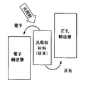
- X is a site that is excited by absorbing light (hereinafter referred to as a light absorption site), Y is a radical in at least one of an oxidized state or a reduced state, and a site that can be repeatedly redox (hereinafter referred to as a radical). (Referred to as site).
- This light-absorbing material has a structure in which an organic dye is bonded to a site that generates a radical in at least one of a photochemical or electrochemical oxidation reaction or reduction reaction.
- the radical site Y is an electron donor for the light absorption site X or an electron acceptor for the light absorption site X.
- the radical site Y promotes the oxidation or reduction reaction of the light-absorbing site X that occurs in the photoelectric conversion process of the light-absorbing material.
- the charge moves between the radical site Y and the light absorption site X, and the light absorption part X is reduced or oxidized, and the radical site Y is oxidized or reduced.
- the holes move from the oxidized radical site Y to the charge transport layer and the like, whereby the radical site Y is reduced, and the electrons move from the reduced light absorption site X to the electron transport layer and the like.
- the light absorption site X is oxidized.
- the radical site Y is an electron acceptor for the light absorption site X
- the light absorption site X is excited by absorbing light, the charge is transferred between the radical site Y and the light absorption site X to absorb light.
- Part X is oxidized and radical site Y is reduced.
- the radical site Y is not an active part that generates radicals but a site that can be a stable radical.
- the state where the spin concentration per molecule of the light-absorbing material is 1 or more continues in an equilibrium state for 1 second or more. Is preferred. In this case, a stable redox reaction occurs under conditions where light is continuously irradiated.
- the oxidized or reduced radical site Y returns to the original state by the hole transport layer or the electron transport layer.
- the upper limit of the spin concentration per molecule of the light-absorbing material is preferably 10,000, but is not limited thereto.
- excited electrons or holes generated by one light absorption site X absorbing light move to one radical site Y, and this radical site Y is reduced or oxidized.
- the light absorbing material is a material having a relatively large molecular weight such as an oligomer structure or a polymer structure and the spin concentration per molecule of the light absorbing material is 2 or more, it is reduced or oxidized by the above process.
- electrons or holes may move to another radical site Y in the same molecule by a self-electron exchange reaction. This is a phenomenon called so-called charge hopping transport. If the spin concentration is as described above, the charges move efficiently.
- the radical spin concentration is quantified by an electron spin resonance apparatus.
- the radical site Y that serves as an electron donor for the light absorption site X will be described.
- the holes move quickly from the light absorption site X to the radical site Y, so that quick charge separation occurs.
- radical site Y that can be an electron donor for the light absorption site X
- examples of the chemical structure of the radical site Y that can be an electron donor for the light absorption site X include the radical structure described in Japanese Patent No. 3687736 and Japanese Patent Application Laid-Open No. 2003-100360.
- the radical site Y that serves as an electron donor for the light-absorbing site X preferably has a nitroxide radical (—NO—). In this case, the photoexcited light absorption site X is reduced by the radical site Y at a higher speed.
- radical site Y having a nitroxide radical include the structures shown in the following structural formulas (2) to (5).
- A represents a binding site interposed between a radical site Y and a light absorption site described later, and A may not exist.
- the radical site Y may contain a hydrazyl radical. Also in this case, the photoexcited light absorption site X is reduced by the radical site Y at a higher speed.
- the radical site Y that can be an electron donor for the light absorption site X is derived from, for example, the compounds shown in the following [Chemical 5] and [Chemical 6].
- the radical site Y that can be an electron donor for the light absorption site X is a radical in the ground state, it needs to be stabilized thermodynamically or kinetically.
- stabilization is achieved by a resonance effect, for example, and in the latter case, stabilization is achieved by a steric effect by, for example, a tetramethyl structure.
- the radical site Y that serves as an electron acceptor for the light absorption site X will be described.
- electrons move quickly from the light absorption site X to the radical site Y, so that quick charge separation occurs.
- the radical site Y that can be an electron acceptor for the light absorption site X includes any of a bipyridinium group, a bipyridinium group having a substituent, a galvinoxyl radical group, and a galvinoxyl radical group having a substituent.
- the radical site Y preferably has a structure represented by the following [Chemical Formula 7] or a structure represented by the following [Chemical Formula 8] as at least a part of its chemical structure.
- the chemical structure of the light-absorbing site X includes the book “Latest Solar Cell Overview” (Information Technology Association) and “FPD / DSSC / Optical memory and the latest technology and material development of functional dyes” (NTS Corporation). ] Ruthenium metal complexes (Ru metal complexes) such as [Ru (4,4′-dicarboxyl-2,2′-bipyridine) 2- (NCS) 2 ] and porphyrin metal complexes; Organic dyes such as indoline-based, coumarin-based, merocyanine-based, and squalinium-based pigments; phthalocyanine-based, dioxazine-based, azo-based (soluble azo-based / insoluble azo-based) pigments, selenium-based, and cynadoline-based pigments; cadmium sulfide, sulfide Examples thereof include semiconductor ultrafine particles such as sulfide semiconductors such as lead and silver sulfide.
- the light absorption site X has a molecular structure of a dye
- the light absorption site X has a so-called donor-acceptor type molecular structure
- charges are separated in the light absorption site X during photoexcitation. It is effective in improving the open circuit voltage and short circuit current of the element.
- the light absorption site X has a chemical structure of an associative dye
- a photoelectric conversion element having excellent characteristics (luminescence efficiency) about 5 times as compared with the case where a conventional ruthenium complex is used can be obtained.
- the light absorption site X has a dye structure as disclosed in Japanese Patent No. 4080288, a radical side reaction is suppressed at the time of light irradiation in a photoelectric conversion element including a light absorption material. The effect (light stabilization effect) is expected.
- the light absorption site X preferably has a structure represented by any of the following general formulas (A) to (C).
- the light absorption site X efficiently absorbs light and photoexcites, so that the redox reaction between the light absorption site X and the radical portion Y proceeds rapidly.
- R ′ is hydrogen, carboxyl group, sulfonyl group, phenyl group, carboxyphenyl group, sulfophenyl group, or pyridinium group, and at least one R ′ is substituted with Y.
- M represents a metal atom.
- M is preferably a transition metal atom such as Zn.
- X 1 and X 2 are each independently a group containing at least one of an alkyl group, an alkenyl group, an aralkyl group, an aryl group, and a heterocyclic ring, and each may have a substituent.
- the radical site Y is bonded to either X 1 or X 2 .
- R ′ is hydrogen, carboxyl group, sulfonyl group, phenyl group, carboxyphenyl group, sulfophenyl group, or pyridinium group, and at least one R ′ is substituted with Y.
- the light absorption site X having a structure shown in the general formula (A) is derived from, for example, a compound shown in the following [Chemical Formula 12].
- the light absorption site X having a structure shown in the general formula (C) is derived from, for example, a compound shown in the following [Chemical Formula 13].
- n is an integer of 0 to 10. In the formula (8), n is an integer of 1 to 20.
- the absorption wavelength range is widened.
- the short circuit current of the conversion element is further improved.
- the light absorbing material may have a binding site A interposed between the radical site Y and the light absorbing site X.
- the binding site A is not essential, and the light absorption site X and the radical site Y may be directly bonded.
- binding site A examples include various divalent groups such as methylene, ethylene, propane-1,3-dienyl, ethylidene, propane-2,2-diyl, alkanediyl, benzylidene, propylene, i-propylene, butylene.
- T-butylene octylene, 2-ethylhexylene, 2-methoxyethylene, benzylene, trifluoromethylene, cyanomethylene, ethoxycarbonylmethylene, propoxyethylene, 3- (1-octylpyridinium-4-yl) propylene, 3- (1-butyl-3-methylpyridinium-4-yl) groups of divalent saturated hydrocarbons which may be substituted, linear or branched, such as propylene; vinylidene, propene-1,3- Groups of divalent unsaturated hydrocarbons such as diyl, but-1-ene-1,4-diyl; Groups of divalent cyclic hydrocarbons such as rhohexanediyl, cyclohexenediyl, cyclohexadienediyl, phenylene, naphthalene, biphenylene; oxalyl, malonyl, succinyl, glutanyl,
- the light absorption part X is an organic material
- the light absorption material has a structure in which the light absorption part X and the radical part Y are ⁇ -conjugated
- the light absorption region of the light absorption material is on the long wavelength side. It is preferable from the viewpoint of movement.
- the photoelectric conversion element includes an electron transport layer or a hole transport layer
- the light absorbing material is bonded to at least one of the electron transport layer and the hole transport layer
- the charge transfer efficiency is further improved.
- the bonding mode between the light absorbing material and the electron transporting layer or the hole transporting layer is not particularly limited.
- the electron transporting layer formed from an oxide semiconductor and the light absorbing material are bonded, the bonding force with the electron transporting layer is reduced.
- a light absorbing material having a group such as a carboxyl group, a sulfo group, or a phosphone group is used. By combining these groups with the electron transport layer, the light absorbing material and the electron transport layer are firmly bonded.
- the electron transport layer formed from the organic semiconductor and the amount of the light absorbing agent are bonded, for example, a light absorbing material having a functional group having high adsorptivity to the organic semiconductor or a functional group causing a chemical bond with the organic semiconductor is used. .
- a light-absorbing material having a radical part Y that serves as an electron donor for the light-absorbing site X is produced, for example, as follows. 4 to 22, “on” means “one night” (overnight), and “rt” means “room temperature” (room temperature).
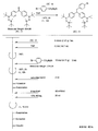
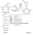
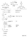
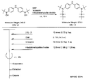
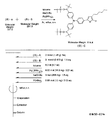
- the light absorbing material represented by the structural formula (6) is manufactured by the steps shown in [Chemical Formula 22], [Chemical Formula 23] and FIGS.
- the compound represented by the structural formula (6) -1 and diethyl ether are mixed with stirring at ⁇ 78 ° C., and tertiary butyl lithium is added thereto. Stir and mix at 78 ° C. for 2 hours, followed by 1 hour at room temperature. 2-Methyl-2-nitrosopropane was added to the resulting mixture, followed by stirring and mixing at ⁇ 78 ° C. for 2 hours, followed by stirring and mixing at room temperature for 10 hours, whereby structural formula (6) — 2 is obtained (yield 40-50%).
- the compound represented by the structural formula (6) -3 and tetrahydrofuran are stirred and mixed at ⁇ 78 ° C., and then the compound represented by the structural formula (6) -a is added.
- the mixture is stirred for 2 hours at ⁇ 78 ° C., and then stirred and mixed for 10 hours at room temperature.
- a saturated solution of monochloroamine, diethyl ether and tetrahydrofuran, and a 10% aqueous hydrochloric acid solution are sequentially added to the resulting mixture, and the mixture is stirred and mixed at room temperature for 10 minutes, whereby the compound represented by the structural formula (6) -4 is obtained. Is obtained (yield 50-60%).
- the compound represented by the structural formula (6) -4, the compound represented by the structural formula (6) -b, tris (dibenzylideneacetone) dipalladium (0), Sodium tertiary riboxide, tritertiarybutylphosphine and toluene are mixed and refluxed overnight to obtain the compound represented by the structural formula (6) -5 (yield 50-60%).
- the compound represented by the structural formula (6) -6, tetra-n-butylammonium fluoride (TBAF), and tetrahydrofuran are stirred at room temperature for 5 hours in an argon atmosphere. After mixing, silver oxide is added and further stirred and mixed at room temperature for 2 hours under an argon atmosphere. As a result, a compound represented by the structural formula (6) is obtained (yield 95-100%).
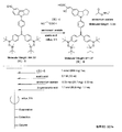
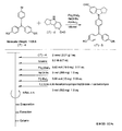
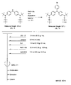
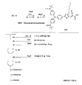
- the light absorbing material represented by the structural formula (7) is manufactured by the steps shown in [Chemical 28], [Chemical 29] and FIGS.
- the compound represented by the structural formula (7) -3 and tetrahydrofuran are stirred and mixed at ⁇ 78 ° C.
- the compound represented by the structural formula (7) -c is added to the mixture thus obtained, mixed at ⁇ 78 ° C. for 2 hours, and then stirred and mixed at room temperature for 10 hours. Further, a saturated solution of monochloroamine, diethyl ether and tetrahydrofuran, and a 10% aqueous hydrochloric acid solution are sequentially added to this mixture, followed by stirring and mixing at room temperature for 10 minutes, whereby a compound represented by the following structural formula (7) -4 is obtained. Is obtained (yield 50-60%).
- the compound represented by the structural formula (7) -4, the compound represented by the structural formula (7) -d, tris (dibenzylideneacetone) dipalladium (0), Sodium tertiary riboxide, tritertiarybutylphosphine, and toluene are mixed and refluxed overnight to obtain a compound represented by the following structural formula (7) -5 (yield: 50-60%) .
- tetra-n-butylammonium fluoride represented by the structural formula (7) -6 and tetrahydrofuran are stirred and mixed at room temperature in an argon atmosphere for 5 hours.
- Silver oxide is further added to the resulting mixture, and the mixture is stirred and mixed at room temperature for 2 hours under an argon atmosphere.
- a compound represented by the structural formula (7) is obtained (yield 95-100%).
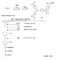
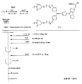
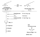
- the light absorbing material represented by the structural formula (8) is manufactured by the steps shown in [Chemical 30] to [Chemical 33] and FIGS.
- the compound represented by the structural formula (8) -1 and diethyl ether are stirred and mixed at ⁇ 78 ° C.
- Tertiary butyllithium is added to the resulting mixture and stirred and mixed at ⁇ 78 ° C. for 2 hours, followed by stirring and mixing at room temperature for 1 hour.
- 2-methyl-2-nitrosopropane was added to this mixture, and the mixture was stirred and mixed at ⁇ 78 ° C. for 2 hours, followed by stirring and mixing at room temperature for 1 hour, thereby showing the structural formula (8) -2. Is obtained (yield 40-50%).
- the compound represented by the structural formula (8) -4, carbon tetrachloride, and N-bromosuccinimide are stirred and mixed at room temperature for 5 hours, whereby the structural formula (8) A compound represented by ⁇ 5 is obtained (yield 50-60%).
- the compound represented by the structural formula (8) -5 and dimethyl ether are stirred and mixed at ⁇ 78 ° C.
- Tertiary butyllithium is added to the resulting mixture, followed by stirring and mixing at ⁇ 78 ° C. for 2 hours, followed by stirring and mixing at room temperature for 1 hour.
- triisopropyl borate is added to this mixture, followed by stirring and mixing at ⁇ 78 ° C. for 2 hours, followed by stirring and mixing at room temperature for 10 hours to obtain a compound represented by the structural formula (8) -B. (Yield 40-50%).
- the compound represented by the structural formula (8) -A, the compound represented by the structural formula (8) -B, toluene, sodium tertiary carboxide, tetra ( (Triphenylphosphinato) palladium is mixed and refluxed overnight under an argon atmosphere to obtain the compound represented by the structural formula (8) -C.
- the compound represented by the structural formula (8) -C 2-cyanoacetic acid, acetonitrile (AN), piperidine, and tetra (triphenylphosphinato) palladium are mixed.
- the compound represented by the structural formula (8) -D is obtained (yield 80 to 90%).
- the compound represented by the structural formula (8) -D, tetra-n-butylammonium fluoride, and tetrahydrofuran are stirred and mixed at room temperature in an argon atmosphere for 5 hours.
- Silver oxide is added to the resulting mixture and stirred and mixed at room temperature for 2 hours under an argon atmosphere.
- a compound represented by the structural formula (8) is obtained (yield 95-100%).
- the compound represented by the structural formula (11) is a fine particle called a quantum dot produced by a method described in “Chemistry Letters” 2007, Vol. 36, No. 6, page 712, for example, “Journal of Molecular. Catalysis A: Chemical ”, 1995, Vol. 101, p. 45, manufactured by binding to a stable free radical by a method as described.
- a light-absorbing material having a radical part Y that serves as an electron acceptor for the light-absorbing site X is produced, for example, as follows.
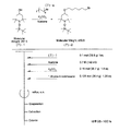
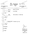
- the light absorbing material represented by the structural formula (14) is manufactured by a chemical reaction represented by the following [Chemical Formula 34], for example.
- a compound represented by the structural formula (14) -1 and a Dl31 dye are added to a tetrahydrofuran (THF) / ethanol mixed solvent, and an ester condensing agent (4- (4,6-dimethoxy-1,3,5) is added.
- an ester condensing agent (4- (4,6-dimethoxy-1,3,5) is added.
- -Triazin-2-yl) -4-methylmorpholinium chloride; DMT-MM) and a base (triethylamine; TEA) are added.
- a compound represented by the structural formula (14) -2 is produced (yield 70%).
- the compound represented by the structural formula (14) -2 is added to ethanol, and an excessive amount of iodomethane is further added.
- the solution thus obtained is left at 60 ° C. overnight, then washed with water and the product is reprecipitated in diethyl ether. Thereby, the reddish brown solid of the light absorption material shown by Structural formula (14) is obtained (yield 65%).
- the light absorbing material represented by the structural formula (14) is soluble in chloroform, acetonitrile, and methanol and insoluble in water.
- the light absorbing material represented by the structural formula (14) is identified by 1H-NMR and FAB-Mass.
- the light absorbing material represented by the structural formula (15) is manufactured by a chemical reaction represented by the following [Chemical Formula 35].
- cyanoacetic acid is dissolved in acetonitrile, and 1-carbonyldiimidazole is further added to activate the carboxyl group.
- a viologen derivative represented by the structural formula (14) -1 synthesized by the reaction represented by [Chemical Formula 30] is added to form an amide bond, and the compound represented by the structural formula (15) -1 Is obtained. Formation of the compound represented by the structural formula (15) -1 is confirmed by FAB-Mass.
- the compound represented by the structural formula (15) -1 is added to ethanol, and further, a base and a D131 dye are added, whereby the compound represented by the structural formula (15) -1 and the D131 dye are condensed.
- a light absorbing material represented by the structural formula (15) is obtained.
- the light absorbing material represented by the structural formula (16) is manufactured by a chemical reaction represented by the following [Chemical Formula 36].
- the compound represented by the structural formula (16) -2 is added to methanol, and a condensing agent (DMT-MM) and a base (triethylamine (TEA)) are further added to the resulting solution.
- a compound represented by the structural formula (16) -3 is obtained (yield 92%).
- the compound represented by Structural Formula (16) -3 is added to ethanol, and an excess amount of iodomethane is further added to the resulting solution.
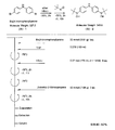
- the light absorbing material represented by the structural formula (17) is manufactured by a chemical reaction represented by the following [Chemical Formula 37].
- a compound represented by the structural formula (17) -1 is formed by a coupling reaction by lithiation of 4- (methoxycarbonyl) phenylboronic acid. Subsequently, PdCl 2 (PPh 3 ) 2 , triethylamine, 4,4,5,5-tetramethyl, and 1,3,2-dioxaborolane are added to the compound represented by the structural formula (17) -1, thereby obtaining The resulting mixture is stirred for 5 hours at 80 ° C. in toluene under an inert atmosphere. Next, liquid separation and HPLC purification of this mixture gives an amber powder of the compound represented by the structural formula (17) -2.
- the compound represented by the structural formula (17) -2 and MD-22 are added in a benzene / water mixed solvent, and Pd (PPh 3 ) 4 and K 2 CO 3 are further added to the resulting solution.
- Pd (PPh 3 ) 4 and K 2 CO 3 are further added to the resulting solution.
- this solution is allowed to stand at 50 ° C. for 12 hours, the reaction proceeds (Suzuki coupling).
- reddish-amber powder of the compound represented by the structural formula (17) -3 is obtained by separation and HPLC purification of this solution.
- the light absorbing material is applied to a photoelectric conversion element such as a dye-sensitized type such as a light emitting element or a solar cell.
- the photoelectric conversion element is composed of, for example, a charge transport material or a conductive substrate for transporting holes and electrons.
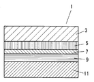
- FIG. 1 is a cross-sectional view showing an example of a dye-sensitized solar cell 1 among photoelectric conversion elements.
- this dye-sensitized solar cell 1 a layer (electron transport layer) formed from the electron transport material 5 between the first substrate electrode 3 and the second substrate electrode 11 disposed so as to face each other.
- a layer formed from the light absorbing material 7 and a layer formed from the charge transport material 9 (hole transport layer) are laminated.
- At least one of the first substrate electrode 3 and the second substrate electrode 11 has translucency.
- the first substrate electrode 3 and the second substrate electrode 11 have conductivity for extracting charges to the outside.
- the translucent substrate electrode may be transparent or opaque, but is particularly preferably transparent.
- the second substrate electrode 11 is formed from a metal foil, the first substrate electrode 3 is preferably formed from a light-transmitting material.
- the first substrate electrode 3 may include a base material formed of, for example, glass or a film.
- the first substrate electrode 3 includes, for example, a conductive layer laminated on a base material.
- the conductive layer is laminated on the surface of the substrate facing the electron transport material 5.
- the conductive layer is made of, for example, a metal such as indium; carbon; a conductive metal oxide such as indium-tin composite oxide, tin oxide doped with antimony or tin oxide doped with fluorine; It is formed from things.
- the first substrate electrode 3 includes a layer formed from the above compound and a layer formed from silicon oxide, tin oxide, titanium oxide, zirconium oxide, aluminum oxide, or the like that coats the layer. Good.
- the first substrate electrode 3 is formed by a dry process such as vapor deposition or sputtering, or a wet process such as dipping, spray pyrolysis, or CVD.
- the first substrate electrode 3 may include a film formed of a metal foil such as titanium, nickel, zinc, and stainless steel.
- the second substrate electrode 11 functions as a negative electrode of the photoelectric conversion element.
- the second substrate electrode 11 is made of only metal, for example.
- the second substrate electrode 11 may include a film and a conductive layer laminated on the film. This conductive layer is in contact with the layer formed from the charge transport material 9.
- the conductive layer in the second substrate electrode 11 is formed of, for example, the same material as the conductive layer in the first substrate electrode 3.
- the conductive layer in the second substrate electrode 11 is, for example, a metal such as platinum, gold, silver, copper, aluminum, rhodium, or indium; a carbon material such as graphite, carbon nanotube, or carbon carrying platinum; an indium-tin composite oxide; It is formed from a conductive metal oxide such as tin oxide doped with antimony or tin oxide doped with fluorine; a conductive polymer such as polyethylenedioxythiophene, polypyrrole or polyaniline.
- the second substrate electrode 11 is preferably formed from platinum, graphite, polyethylenedioxythiophene, or the like.
- the surface resistances of the first substrate electrode 3 and the second substrate electrode 11 are preferably 200 ⁇ / ⁇ or less, and more preferably 50 ⁇ / ⁇ or less.
- the lower limit of the surface resistance range of the first substrate electrode 3 and the second substrate electrode 11 is not particularly limited, but is usually 0.1 ⁇ / ⁇ .
- the light transmittance of the substrate electrode having a high light transmittance is preferably 50% or more, and more preferably 80% or more.
- the thickness of the conductive layer in the first substrate electrode 3 and the second substrate electrode 11 is preferably in the range of 0.1 to 10 ⁇ m. Within this range, a conductive layer having a uniform thickness can be easily formed, and the light transmittance of the conductive layer can be maintained.
- the electron transport material 5 is not particularly limited as long as it is a material using electrons as carriers.
- semiconductor materials used as the electron transport material 5 Cd, Zn, In, Pb, Mo, W, Sb, Bi, Cu, Hg, Ti, Ag, Mn, Fe, V, Sn, Zr, Sr, Ga, Metal element oxides such as Si and Cr; metal oxides having a perovskite structure such as SrTiO 3 and CaTiO 3 ; CdS, ZnS, In 2 S 3 , PbS, Mo 2 S, WS 2 , Sb 2 S 3 , Bi Sulfides such as 2 S 3 , ZnCdS 2 , Cu 2 S; metal chalcogenides such as CdSe, In 2 Se 3 , WSe 2 , HgS, PbSe, CdTe; GaAs, Si, Se, Cd 2 P 3 , Zn 2 P 3 , InP, AgBr, PbI 2 , HgI
- the electron transport material 5 may be a composite containing at least one selected from the semiconductor materials as described above.
- Such composites for example, CdS / TiO 2, CdS / AgI, Ag 2 S / AgI, CdS / ZnO, CdS / HgS, CdS / PbS, ZnO / ZnS, ZnO / ZnSe, CdS / HgS, CdS / CdSe, CdS / Te, CdSe / Te, ZnS / CdSe, ZnSe / CdSe, CdS / ZnS, TiO 2 / Cd 3 P 2 , CdS / CdSe / CdZnS, CdS / HgS / CdS, and the like.
- the electron transport material 5 may be a conductive polymer such as polythiophene or polyaniline, a redox polymer having a redox side chain, C60, or the like that can become an n-type semiconductor by doping.
- the electron transport material 5 may be a polyradical compound which is an n-type semiconductor and exhibits stable oxidation-reduction behavior as disclosed in JP-A-2008-280400.
- the density of molecules of the light absorbing material relative to the projected area of the photoelectric conversion element depends on the light absorption efficiency of the light absorbing material 7 from the viewpoint of output characteristics.
- the range of ⁇ 10 ⁇ 8 to 1 ⁇ 10 ⁇ 6 mol / cm 2 is preferable.
- the density of the light absorbing material 7 is larger than the above range, the amount of the light absorbing material 7 with respect to incident light is too large, so that the amount of the light absorbing material 7 that does not act increases.
- the density of the light absorbing material 7 is smaller than the above range, a sufficient amount of light is not absorbed by the light absorbing material 7.
- the entire photoelectric conversion element is a so-called see-through type element having translucency
- the density and absolute amount of the light-absorbing material 7 are reduced according to the light transmittance desired for the photoelectric conversion element. Also good.
- the layer formed from the electron transport material 5 is porous and the ratio of the effective area to the projected area is 1 or more, the photoelectric conversion efficiency of the photoelectric conversion element is particularly improved.
- the upper limit of the ratio of the effective area to the projected area of the layer formed from the electron transport material 5 is not particularly limited, but is preferably 1 million or less.
- Examples of the charge transport material (hole transport material) 9 include substances that generate redox pairs. As such a charge transport material 9, iodine (I ⁇ / I 3 ⁇ ) is generally used in many cases, but is not limited thereto.
- the charge transport material 9 may be a radical compound that is stably oxidized and reduced as described in JP-A-2003-100360.
- the radical site Y in the light-absorbing material 7 is an electron donor because the reduction reaction of the oxidized radical site Y is promoted and the oxidized radical site Y is rapidly reduced.
- the charge transport material 9 may be an electrolyte solution.
- the solvent used for dissolving the electrolyte is preferably a compound that can dissolve the redox constituent and has excellent ion conductivity.
- the solvent may be either an aqueous solvent or an organic solvent, but an organic solvent is preferable in order to stabilize the oxidation-reduction component in the electrolyte solution.
- organic solvent examples include carbonate compounds such as dimethyl carbonate, diethyl carbonate, methyl ethyl carbonate, ethylene carbonate, and propylene carbonate; ester compounds such as methyl acetate, methyl propionate, and ⁇ -butyrolactone; diethyl ether, 1,2-dimethoxy Ether compounds such as ethane, 1,3-dioxosilane, tetrahydrofuran, 2-methyl-tetrahydrofuran; heterocyclic compounds such as 3-methyl-2-oxazozirinone, 2-methylpyrrolidone; nitrile compounds such as acetonitrile, methoxyacetonitrile, propionitrile Aprotic polar compounds such as sulfolane, dimethyl sulfoxide and dimethylformamide; These solvents may be used alone or in combination of two or more.
- carbonate compounds such as dimethyl carbonate, diethyl carbonate, methyl ethyl carbonate, ethylene carbonate,
- carbonate compounds such as ethylene carbonate and propylene carbonate
- heterocyclic compounds such as ⁇ -butyrolactone, 3-methyl-2-oxazodilinone and 2-methylpyrrolidone
- acetonitrile, methoxyacetonitrile, propionitrile, 3-methoxypropyl Nitrile compounds such as pionitrile and valeric nitrile
- polyol compounds such as ethylene glycol, polyethylene glycol and polyethylene are preferably used.
- the charge transport material 9 may be gelled by containing a polymer matrix such as an oil gel-based or polyvinylidene fluoride-based polymer compound, a liquid crystal gel, a low molecule such as an amino acid derivative, or inorganic particles such as silica particles. .
- a polymer matrix such as an oil gel-based or polyvinylidene fluoride-based polymer compound, a liquid crystal gel, a low molecule such as an amino acid derivative, or inorganic particles such as silica particles.
- the charge transporting material 9 may be a conductive polymer such as polythiophene or polyaniline, a polymer having a side chain that can be easily oxidized or reduced, or the like if it can be a p-type semiconductor by doping. In this case, since the layer formed of the charge transport material 9 is in a solid or gel state, liquid leakage is suppressed, and thus the photoelectric conversion efficiency of the photoelectric conversion element is maintained high over a long period of time.
- the redox potential of the radical site Y and the redox potential of the hole transport material or the electron transport material are adjusted so that charge separation proceeds smoothly.
- the radical site Y in the light absorbing material 7 is an electron donor and the redox potential of the hole transport material 9 is lower than the redox potential of the radical site Y, the charge separation in the light absorbing material 7 is performed. Progresses more smoothly.
- the structure of the radical site Y is a structure as exemplified in the present specification, the potential is adjusted by introducing a functional group into the radical site Y. This can be achieved relatively easily by changing the molecular structure.
- the radical site Y promotes the oxidation or reduction reaction of the light absorption site X, and thus high-speed charge separation. And recombination of charges is suppressed. For this reason, the photoelectric conversion of a photoelectric conversion element becomes high.
- the excited light is generated in the photoelectric conversion process caused by the light absorption site X absorbing light.
- the reduction reaction of the light absorption site X is promoted.
- the radical site Y is oxidized.
- the radical site Y is reduced and holes move from the radical site Y to the hole transport layer.
- the electrons move from the reduced light absorption site X to the electron transport layer, the light absorption site X is oxidized.
- FIG. 3 shows a conventional example.
- the light absorbing material can exhibit the same action as HALS (light stabilizer).
- HALS light stabilizer
- the compound represented by the structural formula (6) -2 (10 mmol (3.56 g) 1 eq), DMF (0.7 M (14.3 ml)) and imidazole (30 mmol (2.10 g) 3 eq) and tertiary butyldimethylsilyl chloride (12.5 mol (1.88 g) 1.25 eq) were stirred and mixed at room temperature for 10 hours to obtain a compound represented by the structural formula (6) -3 ( Yield 80-90%).
- the compound represented by the structural formula (6) -3 (5 mmol (2.92 g) 1 eq) and tetrahydrofuran (0.3 M (16.7 ml)) were stirred and mixed at ⁇ 78 ° C.
- the compound represented by the structural formula (6) -a (15 mol (4.11 g) 1.5 eq) was added to the resulting solution, and the mixture was stirred and mixed at ⁇ 78 ° C. for 2 hours and at room temperature for 10 hours.
- the compound represented by the structural formula (6) -6 (1 mmol (911 mg) 1 eq), TBAF (20 mmol (5.23 g) 20 eq) and THF (50 mM (20 ml)) were added in an argon atmosphere. Under stirring at room temperature for 5 hours, silver oxide (10 mol (2.31 g) 10 eq) was added to the resulting solution and stirred and mixed at room temperature for 2 hours under an argon atmosphere. As a result, a compound represented by the structural formula (6) was obtained (yield 95-100%).
- the compound represented by the structural formula (7) -3 (5 mmol (4.77 g) 1 eq) and tetrahydrofuran (0.3 M (16.7 ml)) were stirred and mixed at ⁇ 78 ° C. Further, the compound represented by the structural formula (7) -c (15 mol (4.11 g) 1.5 eq) was added to the obtained solution and mixed at ⁇ 78 ° C. for 2 hours, and then this solution was stirred at room temperature for 10 hours.
- the compound represented by the structural formula (8) -2 (10 mmol (5.72 g) 1 eq), DMF (0.7 M (14.3 ml)) and imidazole (30 mmol (2.10 g) 3 eq) and tertiary butyldimethylsilyl chloride (12.5 mol (1.88 g) 1.25 eq) were stirred and mixed at room temperature for 10 hours to obtain a compound represented by the structural formula (8) -3 ( Yield 80-90%).
- the compound represented by the structural formula (8) -3 (10 mmol (5.72 g) 1 eq), toluene (0.7 M (14.3 ml)) and sodium tertiary oxide (12. 5 mol (1.20 g) 1.25 eq), copper iodide (1 mmol (0.19 g) 0.1 eq) and piperidine (1.0 mol (85 mg) 0.01 eq) were stirred and mixed, and the resulting solution was mixed with argon. By refluxing in an atmosphere for 5 hours, a compound represented by the structural formula (8) -A was obtained (yield: 50 to 60%).
- the compound represented by the structural formula (8) -4 (0.1 mol (16.8 g) 1 eq), carbon tetrachloride (1M (100 ml)) and N-bromosuccinimide (0. 1 mol (17.8 g) 1 eq) was stirred and mixed at room temperature for 3 hours to obtain a compound represented by the structural formula (8) -5 (yield: 50 to 60%).
- the compound represented by the structural formula (8) -5 50 mmol (12.3 g) 1 eq) and dimethyl ether (0.4 M (125 ml)) were stirred and mixed at ⁇ 78 ° C.
- triisopropyl borate 75 mmol (14.1 g) 1.5 eq
- a compound represented by the formula (8) -B was obtained (yield 40-50%).
- the compound represented by the structural formula (8) -C (1 mmol (0.814 g) 1 eq), 2-cyanoacetic acid (1.2 mmol (0.102 g) 1.2 eq) and AN (0.3 M (6.7 ml)), piperidine (0.03 mmol (2.5 mg) 0.03 eq) and tetra (triphenylphosphinato) palladium (0.01 mmol (12.6 mg) 0.01 eq) were mixed.
- the resulting solution was refluxed for 5 hours under an argon atmosphere to obtain the compound represented by the structural formula (8) -D (yield 80 to 90%).
- the compound represented by the structural formula (8) -D (1 mmol (909 mg) 1 eq), TBAF (20 mmol (5.23 g) 20 eq), and THF (50 mM (20 ml)) are mixed with argon.
- the mixture was stirred and mixed at room temperature for 5 hours under an atmosphere, silver oxide (10 mol (2.31 g) 10 eq) was added to the resulting solution, and the mixture was stirred and mixed at room temperature for 2 hours under an argon atmosphere.
- a compound represented by the structural formula (8) was obtained (yield 95-100%).
- a screen printing paste was obtained by dispersing high-purity titanium oxide powder having an average primary particle diameter of 20 nm in ethyl cellulose.
- a first substrate electrode was produced by forming a 10 nm thick titanium oxide film by sputtering on a 1 mm thick conductive glass substrate (fluorine-doped tin oxide, surface resistance 100 ⁇ / ⁇ ). After applying the screen printing paste on the first substrate electrode, it was dried to form a dry film. This dried film was baked in air at 500 ° C. for 30 minutes. Thereby, a porous titanium oxide film having a thickness of 1.5 ⁇ m was formed on the first substrate electrode.
- the porous titanium oxide film was heated at 70 ° C. for 30 minutes, and then this porous titanium oxide film was used. The membrane was rinsed with distilled water and then air dried. As a result, an electron transport layer was formed on the first substrate electrode.
- Each dimethylformamide solution was prepared. The concentration of the light absorbing material in each solution was 0.2 mM.
- the electron transport layer was immersed in a dimethylformamide solution containing the light absorbing material together with the first substrate electrode, and in this state, the electron transport layer was allowed to stand at room temperature in the dark for 24 hours. Subsequently, the electron transport layer was washed with a solvent.
- a platinum film was formed on the surface of a conductive glass substrate (manufactured by Nippon Sheet Glass, fluorine-doped SnO 2 , surface resistance: 10 ⁇ / ⁇ ) by thermal reduction of chloroplatinic acid to obtain a second substrate electrode.
- the first substrate electrode and the second substrate electrode were opposed to each other so that the electron transport layer was disposed between them. Between this first substrate electrode and the second substrate electrode, a sealing material (hot melt adhesive, trade name Binnel made by Mitsui DuPont Polychemical Co., Ltd.) is removed except for one side of the electron transport layer. Arranged so as to surround. In this state, the first substrate electrode and the second substrate electrode were pressed while being heated, so that both were bonded via a sealing material.
- a sealing material hot melt adhesive, trade name Binnel made by Mitsui DuPont Polychemical Co., Ltd.
- An electrolyte solution was prepared by dissolving at a concentration of 025 mol / dm 3 .
- the electrolyte solution was injected between the first substrate electrode and the second substrate electrode through a gap that was not blocked by the sealing material. Subsequently, the gap that was not blocked by the sealing material was blocked with an ultraviolet curable resin. Thereby, a photoelectric conversion element having a light receiving area of 1 cm 2 was obtained.
- Example 4 A first substrate electrode was obtained by forming a fluorine-doped SnO 2 layer on a 1 mm thick conductive glass substrate (manufactured by Asahi Glass Co., Ltd., surface resistance 10 ⁇ / ⁇ ).
- a platinum plate was prepared as the second substrate electrode.
- the second substrate electrode and the first substrate electrode were opposed to each other so that a film of a light absorbing material was disposed between them, and the space between them was surrounded by a sealing material. Subsequently, the first substrate electrode and the second substrate electrode were pressurized while being heated, so that both were bonded together via a sealing material.
- the open-circuit voltage of this photoelectric conversion element under light irradiation was 480 mV, and when the light was cut off, the output voltage gradually converged to 0 mV. When the light was irradiated again, the open circuit voltage converged to 480 mV. This light response behavior was repeatedly and stably expressed.
- Example 7 Instead of the light absorbing material represented by the structural formula (14), the light absorbing material represented by the structural formula (15) in Example 5, the light absorbing material represented by the structural formula (16) in Example 6, and Example 7 Then, the light absorption material shown by Structural formula (17) was used, respectively. Otherwise, a photoelectric conversion element was produced under the same method and conditions as in Example 4.
- the open-circuit voltage of this photoelectric conversion element was measured in the same manner as in Example 4. As a result, it was 430 mV in Example 5, 410 mV in Example 6, and 380 mV in Example 7. A behavior was developed.
- the open circuit voltage of this photoelectric conversion element under light irradiation was 90 mV, and when the light was cut off, the output voltage gradually converged to 0 mV. When light was irradiated again, the open circuit voltage converged to 90 mV. This light response behavior was repeatedly and stably expressed.
- the open-circuit voltage of this photoelectric conversion element under light irradiation was 40 mV, and when the light was cut off, the output voltage gradually converged to 0 mV. Furthermore, when light was irradiated again, the output voltage converged to 40 mV. This light response behavior was repeatedly and stably expressed.
Abstract
Description
Xは光吸収部位を、Yは酸化状態または還元状態の少なくとも一方においてラジカルとなり且つ繰り返し酸化還元可能なラジカル部位を、それぞれ示す。 XY (1)
X represents a light absorption site, and Y represents a radical site that can be a radical in at least one of an oxidized state and a reduced state and can be repeatedly oxidized and reduced.


Xは光を吸収することで励起して励起電子を生じる部位(以下、光吸収部位という)を、Yは酸化状態または還元状態の少なくとも一方においてラジカルとなり且つ繰り返し酸化還元可能な部位(以下、ラジカル部位という)を、それぞれ示す。この光吸収材料は、有機色素に、光化学的又は電気化学的な酸化反応又は還元反応の少なくとも一方の過程でラジカルを生成する部位が結合したような構造を有する。 XY (1)
X is a site that is excited by absorbing light (hereinafter referred to as a light absorption site), Y is a radical in at least one of an oxidized state or a reduced state, and a site that can be repeatedly redox (hereinafter referred to as a radical). (Referred to as site). This light-absorbing material has a structure in which an organic dye is bonded to a site that generates a radical in at least one of a photochemical or electrochemical oxidation reaction or reduction reaction.


<光吸収材料の合成>
((6)で示す光吸収材料の製造)
図4に示すように、構造式(6)-1で示される化合物(30mmol(10.2g)1eq)とジエチルエーテル(ether)(0.2M(150ml))とを-78℃で撹拌混合し、得られた溶液にターシャリーブチルリチウム(0.27mol(170ml,d=1.6M)9eq)を加えて-78℃で2時間及び室温で1時間撹拌混合し、次にこの溶液に2-メチル-2-ニトロソプロパン(90mmol(7.84g)3eq)を加えて-78℃で2時間及び室温で10時間撹拌混合することで、構造式(6)-2に示される化合物を得た(収率40~50%)。 (Examples 1 to 3)
<Synthesis of light absorbing material>
(Manufacture of light absorbing material shown in (6))
As shown in FIG. 4, the compound represented by the structural formula (6) -1 (30 mmol (10.2 g) 1 eq) and diethyl ether (0.2 M (150 ml)) were stirred and mixed at −78 ° C. Then, tertiary butyl lithium (0.27 mol (170 ml, d = 1.6 M) 9 eq) was added to the resulting solution, and the mixture was stirred and mixed at −78 ° C. for 2 hours and at room temperature for 1 hour. Methyl-2-nitrosopropane (90 mmol (7.84 g) 3 eq) was added, and the mixture was stirred and mixed at −78 ° C. for 2 hours and at room temperature for 10 hours to obtain the compound represented by the structural formula (6) -2 ( Yield 40-50%).
図10に示すように、構造式(7)-1で示される化合物(0.1mol(28.8g)1eq)と構造式(7)-aで示される化合物(0.125mol(36.4g)1.25eq)と炭酸カリウム(0.15mol(20.7g)1.5eq)とアセトン(0.7M(142ml))を混合し、得られた溶液を一晩還流することで、構造式(7)-2に示される化合物を得た(収率95~100%)。 (Manufacture of light absorbing material shown in (7))
As shown in FIG. 10, the compound represented by Structural Formula (7) -1 (0.1 mol (28.8 g) 1 eq) and the compound represented by Structural Formula (7) -a (0.125 mol (36.4 g)) 1.25 eq), potassium carbonate (0.15 mol (20.7 g) 1.5 eq) and acetone (0.7 M (142 ml)) were mixed, and the resulting solution was refluxed overnight to obtain the structural formula (7 ) -2 was obtained (yield 95-100%).
図16に示すように、構造式(8)-1で示される化合物(30mmol(9.81g)1eq)とジエチルエーテル(ether)とを-78℃で撹拌混合し、得られた溶液に更にターシャリーブチルリチウム(0.27mol(170ml,d=1.6M)9eq)を加えて-78℃で2時間及び室温で1時間攪拌混合し、次にこの溶液に2-メチル-2-ニトロソプロパン(90mmol(7.84g)3eq)を加えて-78℃で2時間攪拌混合し、続いてこの溶液を室温で1時間攪拌混合することで、構造式(8)-2で示される化合物を得た(収率40~50%)。 (Manufacture of light absorbing material shown in (8))
As shown in FIG. 16, the compound represented by the structural formula (8) -1 (30 mmol (9.81 g) 1 eq) and diethyl ether (ether) were stirred and mixed at −78 ° C., and the resulting solution was further mixed with tarsier. Libutylbutyllithium (0.27 mol (170 ml, d = 1.6 M) 9 eq) was added and stirred and mixed at −78 ° C. for 2 hours and at room temperature for 1 hour, and then this solution was mixed with 2-methyl-2-nitrosopropane ( 90 mmol (7.84 g) 3 eq) was added and stirred and mixed at −78 ° C. for 2 hours, and then this solution was stirred and mixed at room temperature for 1 hour to obtain the compound represented by the structural formula (8) -2. (Yield 40-50%).
平均1次粒子径が20nmの高純度酸化チタン粉末をエチルセルロース中に分散させることで、スクリーン印刷用のペーストを得た。 <Production of photoelectric conversion element (dye-sensitized solar cell)>
A screen printing paste was obtained by dispersing high-purity titanium oxide powder having an average primary particle diameter of 20 nm in ethyl cellulose.
構造式(6)~(8)で示される光吸収材料を用いず、それに代えて三菱製紙株式会社製のD131色素を用いた。それ以外は実施例1の場合と同じ方法及び条件で、光電変換素子を作製した。 (Comparative Example 1)
The light absorbing material represented by the structural formulas (6) to (8) was not used, and D131 dye manufactured by Mitsubishi Paper Industries Co., Ltd. was used instead. Other than that was the photoelectric conversion element by the same method and conditions as the case of Example 1.
各実施例及び比較例で得られた光電変換素子に照度200Lxの光を照射した場合の、光電変換素子の電流-電位特性を測定し、最大出力Pmax(W/cm2)を導出した。その結果を、比較例1の最大出力Pmaxを100として規格化し、下記表1に示す。 (Evaluation)
When the photoelectric conversion elements obtained in the respective examples and comparative examples were irradiated with light having an illuminance of 200 Lx, the current-potential characteristics of the photoelectric conversion elements were measured, and the maximum output P max (W / cm 2 ) was derived. The results are normalized with the maximum output P max of Comparative Example 1 as 100, and are shown in Table 1 below.

厚み1mmの導電性ガラス基板(旭硝子株式会社製、表面抵抗10Ω/□)の上に、フッ素ドープSnO2の層を形成することで、第一の基板電極を得た。 Example 4
A first substrate electrode was obtained by forming a fluorine-doped SnO 2 layer on a 1 mm thick conductive glass substrate (manufactured by Asahi Glass Co., Ltd., surface resistance 10Ω / □).
構造式(14)で示される光吸収材料に代えて、実施例5では構造式(15)で示される光吸収材料、実施例6では構造式(16)で示される光吸収材料、実施例7では構造式(17)で示される光吸収材料を、それぞれ使用した。それ以外は実施例4と同じ方法及び条件で、光電変換素子を作製した。 (Examples 5 to 7)
Instead of the light absorbing material represented by the structural formula (14), the light absorbing material represented by the structural formula (15) in Example 5, the light absorbing material represented by the structural formula (16) in Example 6, and Example 7 Then, the light absorption material shown by Structural formula (17) was used, respectively. Otherwise, a photoelectric conversion element was produced under the same method and conditions as in Example 4.
5mlのN,N-ジメチルホルムアミド中に、三菱製紙株式会社製のD131色素を5mg、及びビオロゲンを5mg加えて溶解させ、得られた溶液を第一の基板電極上にドロップキャスト法により塗布することで、厚み50nmの膜を形成した。実施例4におけるような光吸収材料の膜は形成しなかった。それ以外は実施例4と同じ方法及び条件で、光電変換素子を作製した。 (Comparative Example 2)
In 5 ml of N, N-dimethylformamide, 5 mg of D131 dye and 5 mg of viologen manufactured by Mitsubishi Paper Industries, Ltd. are added and dissolved, and the resulting solution is applied onto the first substrate electrode by the drop cast method. Thus, a film having a thickness of 50 nm was formed. A film of light absorbing material as in Example 4 was not formed. Otherwise, a photoelectric conversion element was produced under the same method and conditions as in Example 4.
5mlのN,N-ジメチルホルムアミド中に、三菱製紙株式会社製のD131色素を5mg、及びガルビノキシルを5mg加えて溶解させ、得られた溶液を第一の基板電極上にドロップキャスト法により塗布することで、厚み50nmの膜を形成した。実施例4におけるような光吸収材料の膜は形成しなかった。それ以外は実施例4と同じ方法及び条件で、光電変換素子を作製した。 (Comparative Example 3)
In 5 ml of N, N-dimethylformamide, 5 mg of D131 dye manufactured by Mitsubishi Paper Industries, Ltd. and 5 mg of galvinoxyl are added and dissolved, and the resulting solution is applied onto the first substrate electrode by the drop cast method. Thus, a film having a thickness of 50 nm was formed. A film of light absorbing material as in Example 4 was not formed. Otherwise, a photoelectric conversion element was produced under the same method and conditions as in Example 4.
Claims (7)
- 下記の式(1)で表される構造を有する光吸収材料。
X-Y …(1)
Xは光吸収部位を、Yは酸化状態または還元状態の少なくとも一方においてラジカルとなり且つ繰り返し酸化還元可能なラジカル部位を、それぞれ示す。 The light absorption material which has a structure represented by following formula (1).
XY (1)
X represents a light absorption site, and Y represents a radical site that can be a radical in at least one of an oxidized state and a reduced state and can be repeatedly oxidized and reduced. - 前記式(1)におけるYが、Xに対する電子供与体である請求項1に記載の光吸収材料。 The light absorbing material according to claim 1, wherein Y in the formula (1) is an electron donor for X.
- 前記式(1)におけるYが、ニトロキシドラジカルである請求項2に記載の光吸収材料。 The light absorbing material according to claim 2, wherein Y in the formula (1) is a nitroxide radical.
- 前記式(1)におけるYが、Xに対する電子受容体である請求項1に記載の光吸収材料。 The light absorbing material according to claim 1, wherein Y in the formula (1) is an electron acceptor for X.
- 前記式(1)におけるYが、ビピリジニウム基、置換基を有するビピリジニウム基、ガルビノキシルラジカル基、及び置換基を有するガルビノキシルラジカル基のうち、いずれかを含む請求項4に記載の光吸収材料。 The light absorption according to claim 4, wherein Y in the formula (1) includes any one of a bipyridinium group, a bipyridinium group having a substituent, a galvinoxyl radical group, and a galvinoxyl radical group having a substituent. material.
- 前記式(1)におけるXが、下記一般式(A)乃至(C)のいずれかで示される構造を有する請求項4に記載の光吸収材料。


- 請求項1に記載の光吸収材料と、電子輸送層と、正孔輸送層とを備える光電変換素子。 A photoelectric conversion element comprising the light absorbing material according to claim 1, an electron transport layer, and a hole transport layer.
Priority Applications (4)
| Application Number | Priority Date | Filing Date | Title |
|---|---|---|---|
| US13/322,048 US8729532B2 (en) | 2009-05-22 | 2010-05-21 | Light-absorbing material and photoelectric conversion element |
| KR1020117030731A KR101366122B1 (en) | 2009-05-22 | 2010-05-21 | Light-absorbing material and photoelectric conversion element |
| EP10777838.3A EP2433989B1 (en) | 2009-05-22 | 2010-05-21 | Light-absorbing material and photoelectric conversion element |
| CN201080022143.2A CN102439092B (en) | 2009-05-22 | 2010-05-21 | Light-absorbing material and photoelectric conversion element |
Applications Claiming Priority (2)
| Application Number | Priority Date | Filing Date | Title |
|---|---|---|---|
| JP2009124522 | 2009-05-22 | ||
| JP2009-124522 | 2009-05-22 |
Publications (1)
| Publication Number | Publication Date |
|---|---|
| WO2010134607A1 true WO2010134607A1 (en) | 2010-11-25 |
Family
ID=43126284
Family Applications (1)
| Application Number | Title | Priority Date | Filing Date |
|---|---|---|---|
| PCT/JP2010/058662 WO2010134607A1 (en) | 2009-05-22 | 2010-05-21 | Light-absorbing material and photoelectric conversion element |
Country Status (7)
| Country | Link |
|---|---|
| US (1) | US8729532B2 (en) |
| EP (1) | EP2433989B1 (en) |
| JP (1) | JP5711470B2 (en) |
| KR (1) | KR101366122B1 (en) |
| CN (1) | CN102439092B (en) |
| TW (1) | TW201107457A (en) |
| WO (1) | WO2010134607A1 (en) |
Cited By (3)
| Publication number | Priority date | Publication date | Assignee | Title |
|---|---|---|---|---|
| WO2012121192A1 (en) * | 2011-03-10 | 2012-09-13 | パナソニック株式会社 | Light-absorbing material and photoelectric conversion element |
| JP2015074754A (en) * | 2013-10-11 | 2015-04-20 | 三菱製紙株式会社 | Organic dye |
| JP2015097259A (en) * | 2013-10-11 | 2015-05-21 | パナソニック株式会社 | Photoelectric conversion element |
Families Citing this family (13)
| Publication number | Priority date | Publication date | Assignee | Title |
|---|---|---|---|---|
| US20130220822A1 (en) * | 2010-11-08 | 2013-08-29 | Bjorn Winther-Jensen | Method and system for catalysis |
| JP5996255B2 (en) * | 2011-05-09 | 2016-09-21 | 旭化成株式会社 | Photoelectric conversion element and π-conjugated organic radical compound |
| WO2013099689A1 (en) | 2011-12-28 | 2013-07-04 | パナソニック株式会社 | Photoelectric element |
| US8952372B2 (en) | 2011-12-28 | 2015-02-10 | Panasonic Corporation | Photoelectric element and method for producing the same |
| TWI470776B (en) * | 2011-12-29 | 2015-01-21 | Ind Tech Res Inst | Light detecting array structure and light detecting module |
| WO2013140181A1 (en) * | 2012-03-22 | 2013-09-26 | The University Of Manchester | Photovoltaic cells |
| CN104797644A (en) * | 2012-12-03 | 2015-07-22 | 阿克伦大学 | An organic polymer photo device with broadband response and increased photo-responsitivity |
| CN104112787B (en) * | 2014-07-28 | 2016-04-13 | 武汉鑫神光电科技有限公司 | A kind of silver sulfide/perovskite bulk heterojunction solar cell and preparation method thereof |
| WO2016181962A1 (en) * | 2015-05-12 | 2016-11-17 | 住友化学株式会社 | Organic photoelectric conversion element |
| WO2017043871A1 (en) * | 2015-09-07 | 2017-03-16 | 주식회사 레이언스 | X-ray detector |
| KR20170029371A (en) | 2015-09-07 | 2017-03-15 | 주식회사 레이언스 | X-ray detector |
| CN113130769B (en) * | 2021-04-09 | 2023-10-13 | 东南大学 | Two-dimensional layered perovskite single crystal, wide-spectrum photoelectric detector and preparation method thereof |
| JP7294601B2 (en) * | 2021-07-13 | 2023-06-20 | 独立行政法人国立高等専門学校機構 | Method for manufacturing photoelectric conversion element, photoelectric conversion element, method for manufacturing n-type semiconductor layer in photoelectric conversion element |
Citations (9)
| Publication number | Priority date | Publication date | Assignee | Title |
|---|---|---|---|---|
| JP2664194B2 (en) | 1988-02-12 | 1997-10-15 | エコル ポリテクニク フェデラル ドゥ ローザンヌ | Photoelectrochemical cells, their production and use |
| JP2003100360A (en) | 2001-09-26 | 2003-04-04 | Nec Corp | Optoelectrochemical device |
| JP3687736B2 (en) | 2000-02-25 | 2005-08-24 | 日本電気株式会社 | Secondary battery |
| JP2007262263A (en) * | 2006-03-29 | 2007-10-11 | Fujifilm Corp | Phthalocyanine compound |
| JP4080288B2 (en) | 2002-09-26 | 2008-04-23 | 三菱製紙株式会社 | Merocyanine dyes for solar cells |
| JP2008201912A (en) * | 2007-02-20 | 2008-09-04 | Fujifilm Corp | Photopolymerizable composition |
| JP2008280400A (en) | 2007-05-09 | 2008-11-20 | Nec Corp | Polyradical compound and battery |
| JP2009021212A (en) * | 2007-06-14 | 2009-01-29 | Panasonic Electric Works Co Ltd | Photoelectric conversion element |
| JP2009081141A (en) * | 2006-02-02 | 2009-04-16 | Sony Corp | Dye-sensitized photoelectric conversion device |
Family Cites Families (3)
| Publication number | Priority date | Publication date | Assignee | Title |
|---|---|---|---|---|
| EP2009064B1 (en) * | 2002-07-29 | 2012-10-24 | Mitsubishi Paper Mills Limited | Organic dye, photoelectric transducing material, semiconductor electrode, and photoelectric transducing device |
| JP2007234580A (en) * | 2006-02-02 | 2007-09-13 | Sony Corp | Dye sensitized photoelectric conversion device |
| JP5023866B2 (en) | 2007-07-27 | 2012-09-12 | ソニー株式会社 | Dye-sensitized photoelectric conversion element, method for producing the same, and electronic device |
-
2010
- 2010-05-21 WO PCT/JP2010/058662 patent/WO2010134607A1/en active Application Filing
- 2010-05-21 US US13/322,048 patent/US8729532B2/en active Active
- 2010-05-21 CN CN201080022143.2A patent/CN102439092B/en active Active
- 2010-05-21 EP EP10777838.3A patent/EP2433989B1/en active Active
- 2010-05-21 JP JP2010117398A patent/JP5711470B2/en active Active
- 2010-05-21 KR KR1020117030731A patent/KR101366122B1/en active IP Right Grant
- 2010-05-21 TW TW099116307A patent/TW201107457A/en unknown
Patent Citations (9)
| Publication number | Priority date | Publication date | Assignee | Title |
|---|---|---|---|---|
| JP2664194B2 (en) | 1988-02-12 | 1997-10-15 | エコル ポリテクニク フェデラル ドゥ ローザンヌ | Photoelectrochemical cells, their production and use |
| JP3687736B2 (en) | 2000-02-25 | 2005-08-24 | 日本電気株式会社 | Secondary battery |
| JP2003100360A (en) | 2001-09-26 | 2003-04-04 | Nec Corp | Optoelectrochemical device |
| JP4080288B2 (en) | 2002-09-26 | 2008-04-23 | 三菱製紙株式会社 | Merocyanine dyes for solar cells |
| JP2009081141A (en) * | 2006-02-02 | 2009-04-16 | Sony Corp | Dye-sensitized photoelectric conversion device |
| JP2007262263A (en) * | 2006-03-29 | 2007-10-11 | Fujifilm Corp | Phthalocyanine compound |
| JP2008201912A (en) * | 2007-02-20 | 2008-09-04 | Fujifilm Corp | Photopolymerizable composition |
| JP2008280400A (en) | 2007-05-09 | 2008-11-20 | Nec Corp | Polyradical compound and battery |
| JP2009021212A (en) * | 2007-06-14 | 2009-01-29 | Panasonic Electric Works Co Ltd | Photoelectric conversion element |
Non-Patent Citations (15)
| Title |
|---|
| CHEMISTRY LETTERS, vol. 36, no. 6, 2007, pages 712 |
| J. AM. CHEM. SOC., vol. 117, 1995, pages 2049 - 2057, XP008148190 * |
| J. AM. CHEM. SOC., vol. 122, 2000, pages 11480 - 11487, XP008148189 * |
| J. PHYS. CHEM. A, vol. 106, 2002, pages 4453 - 4467, XP002971037 * |
| JAPANESE JOURNAL OF POLYMER SCIENCE AND TECHNOLOGY, vol. 37, no. 10, 1980, pages 635 - 640, XP008148172 * |
| JOURNAL OF MAGNETIC RESONANCE, vol. 131, 1998, pages 97 - 110, XP004407512 * |
| JOURNAL OF MAGNETIC RESONANCE, vol. 52, 1983, pages 435 - 449, XP023958607 * |
| JOURNAL OF MAGNETIC RESONANCE, vol. 60, 1984, pages 54 - 65, XP023956226 * |
| JOURNAL OF MOLECULAR CATALYSIS A: CHEMICAL, vol. 101, 1995, pages 45 |
| JOURNAL OF MOLECULAR CATALYSIS B: ENZYMATIC, vol. 17, 2002, pages 9 - 21, XP008148170 * |
| JOURNAL OF PHOTOCHEMISTRY AND PHOTOBIOLOGY A: CHEMISTRY, vol. 133, 2000, pages 105 - 114, XP008148191 * |
| MOLECULAR PHYSICS, vol. 100, no. 9, 2002, pages 1459 - 1468, XP008148227 * |
| PHYSICAL CHEMISTRY CHEMICAL PHYSICS, vol. 7, 2005, pages 4114 - 4125, XP008148224 * |
| See also references of EP2433989A4 |
| TETRAHEDRON LETTERS, vol. 47, 2006, pages 5637 - 5640, XP025004598 * |
Cited By (3)
| Publication number | Priority date | Publication date | Assignee | Title |
|---|---|---|---|---|
| WO2012121192A1 (en) * | 2011-03-10 | 2012-09-13 | パナソニック株式会社 | Light-absorbing material and photoelectric conversion element |
| JP2015074754A (en) * | 2013-10-11 | 2015-04-20 | 三菱製紙株式会社 | Organic dye |
| JP2015097259A (en) * | 2013-10-11 | 2015-05-21 | パナソニック株式会社 | Photoelectric conversion element |
Also Published As
| Publication number | Publication date |
|---|---|
| JP2011006665A (en) | 2011-01-13 |
| TW201107457A (en) | 2011-03-01 |
| KR20120023124A (en) | 2012-03-12 |
| KR101366122B1 (en) | 2014-02-25 |
| EP2433989A4 (en) | 2014-04-02 |
| US8729532B2 (en) | 2014-05-20 |
| CN102439092B (en) | 2014-10-08 |
| EP2433989A1 (en) | 2012-03-28 |
| EP2433989B1 (en) | 2018-03-14 |
| CN102439092A (en) | 2012-05-02 |
| US20120181516A1 (en) | 2012-07-19 |
| JP5711470B2 (en) | 2015-04-30 |
Similar Documents
| Publication | Publication Date | Title |
|---|---|---|
| JP5711470B2 (en) | Light absorbing material and photoelectric conversion element | |
| JP4841248B2 (en) | Dye-sensitized photoelectric conversion element | |
| JP5106381B2 (en) | Dye-sensitized photoelectric conversion element | |
| JP5204848B2 (en) | Photoelectric element | |
| JP4963343B2 (en) | Dye-sensitized photoelectric conversion element | |
| JP5138371B2 (en) | Dye-sensitized photoelectric conversion element | |
| US20110011456A1 (en) | Photosensitizer and solar cell using the same | |
| JP2011034813A (en) | Photoelectric element | |
| JP4450573B2 (en) | Dye-sensitized photoelectric conversion element | |
| JP4230228B2 (en) | Dye-sensitized photoelectric conversion element | |
| JP5957012B2 (en) | Photoelectric element | |
| JP5794589B2 (en) | Dye-sensitized solar cell and sensitizing dye | |
| WO2012121192A1 (en) | Light-absorbing material and photoelectric conversion element | |
| JP5584447B2 (en) | Photoelectric element | |
| KR20080103683A (en) | Novel julolidine-based dye and preparation thereof | |
| JP6616907B2 (en) | Photoelectric conversion element, dye-sensitized solar cell, metal complex dye, dye solution, and oxide semiconductor electrode | |
| KR20130007287A (en) | Dye for dye-sensitized solarcell, preparation method of the same and dye-sensitized solar cell comprising the same | |
| JP6591691B2 (en) | Photoelectric conversion element, dye-sensitized solar cell, and dipyrromethene complex compound | |
| JP2008186632A (en) | Photoelectric conversion element and its manufacturing method | |
| JP2008226582A (en) | Photoelectric conversion element and solar cell | |
| WO2018047498A1 (en) | Photoelectric conversion element, dye-sensitized solar cell and dipyrromethene complex compound | |
| KR101150507B1 (en) | X-shaped conjugated organic compound, dye-sensitized photoelectric converter and dye-sensitized solar cells using the compound | |
| JP5250989B2 (en) | Photoelectric conversion element and solar cell | |
| JP2013185029A (en) | Dyestuff for opto-electronic device, opto-electronic device and method of manufacturing the same |
Legal Events
| Date | Code | Title | Description |
|---|---|---|---|
| WWE | Wipo information: entry into national phase |
Ref document number: 201080022143.2 Country of ref document: CN |
|
| 121 | Ep: the epo has been informed by wipo that ep was designated in this application |
Ref document number: 10777838 Country of ref document: EP Kind code of ref document: A1 |
|
| NENP | Non-entry into the national phase |
Ref country code: DE |
|
| WWE | Wipo information: entry into national phase |
Ref document number: 2010777838 Country of ref document: EP |
|
| ENP | Entry into the national phase |
Ref document number: 20117030731 Country of ref document: KR Kind code of ref document: A |
|
| WWE | Wipo information: entry into national phase |
Ref document number: 13322048 Country of ref document: US |