EP2433989B1 - Light-absorbing material and photoelectric conversion element - Google Patents
Light-absorbing material and photoelectric conversion element Download PDFInfo
- Publication number
- EP2433989B1 EP2433989B1 EP10777838.3A EP10777838A EP2433989B1 EP 2433989 B1 EP2433989 B1 EP 2433989B1 EP 10777838 A EP10777838 A EP 10777838A EP 2433989 B1 EP2433989 B1 EP 2433989B1
- Authority
- EP
- European Patent Office
- Prior art keywords
- light
- structural formula
- site
- group
- compound represented
- Prior art date
- Legal status (The legal status is an assumption and is not a legal conclusion. Google has not performed a legal analysis and makes no representation as to the accuracy of the status listed.)
- Active
Links
- 0 *c(cc1)cc2c1N(*)C1C2CCC1 Chemical compound *c(cc1)cc2c1N(*)C1C2CCC1 0.000 description 3
- SSQQUEKFNSJLKX-UHFFFAOYSA-N CC(C)(C)c1cc(Br)cc(C(C)(C)C)c1O Chemical compound CC(C)(C)c1cc(Br)cc(C(C)(C)C)c1O SSQQUEKFNSJLKX-UHFFFAOYSA-N 0.000 description 1
- PFONWVKNRHEVHJ-UHFFFAOYSA-M CC(C)(C)c1cc(C(c(cc2)ccc2S)=C(C=C2C(C)(C)C)C=C(C(C)(C)C)C2=O)cc(C(C)(C)C)c1[O-] Chemical compound CC(C)(C)c1cc(C(c(cc2)ccc2S)=C(C=C2C(C)(C)C)C=C(C(C)(C)C)C2=O)cc(C(C)(C)C)c1[O-] PFONWVKNRHEVHJ-UHFFFAOYSA-M 0.000 description 1
- ZOYVJOJXRNBJSD-UHFFFAOYSA-N CC(C)(C)c1cc(C(c(cc2)ccc2S2OC(C)(C)C(C)(C)O2)=C(C=C2C(C)(C)C)C=C(C(C)(C)C)C2=O)cc(C(C)(C)C)c1O Chemical compound CC(C)(C)c1cc(C(c(cc2)ccc2S2OC(C)(C)C(C)(C)O2)=C(C=C2C(C)(C)C)C=C(C(C)(C)C)C2=O)cc(C(C)(C)C)c1O ZOYVJOJXRNBJSD-UHFFFAOYSA-N 0.000 description 1
- UCFSYHMCKWNKAH-UHFFFAOYSA-N CC1(C)OBOC1(C)C Chemical compound CC1(C)OBOC1(C)C UCFSYHMCKWNKAH-UHFFFAOYSA-N 0.000 description 1
Images


Classifications
-
- H—ELECTRICITY
- H01—ELECTRIC ELEMENTS
- H01M—PROCESSES OR MEANS, e.g. BATTERIES, FOR THE DIRECT CONVERSION OF CHEMICAL ENERGY INTO ELECTRICAL ENERGY
- H01M14/00—Electrochemical current or voltage generators not provided for in groups H01M6/00 - H01M12/00; Manufacture thereof
- H01M14/005—Photoelectrochemical storage cells
-
- C—CHEMISTRY; METALLURGY
- C09—DYES; PAINTS; POLISHES; NATURAL RESINS; ADHESIVES; COMPOSITIONS NOT OTHERWISE PROVIDED FOR; APPLICATIONS OF MATERIALS NOT OTHERWISE PROVIDED FOR
- C09B—ORGANIC DYES OR CLOSELY-RELATED COMPOUNDS FOR PRODUCING DYES, e.g. PIGMENTS; MORDANTS; LAKES
- C09B69/00—Dyes not provided for by a single group of this subclass
-
- C—CHEMISTRY; METALLURGY
- C09—DYES; PAINTS; POLISHES; NATURAL RESINS; ADHESIVES; COMPOSITIONS NOT OTHERWISE PROVIDED FOR; APPLICATIONS OF MATERIALS NOT OTHERWISE PROVIDED FOR
- C09B—ORGANIC DYES OR CLOSELY-RELATED COMPOUNDS FOR PRODUCING DYES, e.g. PIGMENTS; MORDANTS; LAKES
- C09B11/00—Diaryl- or thriarylmethane dyes
- C09B11/02—Diaryl- or thriarylmethane dyes derived from diarylmethanes
-
- C—CHEMISTRY; METALLURGY
- C09—DYES; PAINTS; POLISHES; NATURAL RESINS; ADHESIVES; COMPOSITIONS NOT OTHERWISE PROVIDED FOR; APPLICATIONS OF MATERIALS NOT OTHERWISE PROVIDED FOR
- C09B—ORGANIC DYES OR CLOSELY-RELATED COMPOUNDS FOR PRODUCING DYES, e.g. PIGMENTS; MORDANTS; LAKES
- C09B23/00—Methine or polymethine dyes, e.g. cyanine dyes
- C09B23/0008—Methine or polymethine dyes, e.g. cyanine dyes substituted on the polymethine chain
-
- C—CHEMISTRY; METALLURGY
- C09—DYES; PAINTS; POLISHES; NATURAL RESINS; ADHESIVES; COMPOSITIONS NOT OTHERWISE PROVIDED FOR; APPLICATIONS OF MATERIALS NOT OTHERWISE PROVIDED FOR
- C09B—ORGANIC DYES OR CLOSELY-RELATED COMPOUNDS FOR PRODUCING DYES, e.g. PIGMENTS; MORDANTS; LAKES
- C09B23/00—Methine or polymethine dyes, e.g. cyanine dyes
- C09B23/10—The polymethine chain containing an even number of >CH- groups
- C09B23/105—The polymethine chain containing an even number of >CH- groups two >CH- groups
-
- C—CHEMISTRY; METALLURGY
- C09—DYES; PAINTS; POLISHES; NATURAL RESINS; ADHESIVES; COMPOSITIONS NOT OTHERWISE PROVIDED FOR; APPLICATIONS OF MATERIALS NOT OTHERWISE PROVIDED FOR
- C09B—ORGANIC DYES OR CLOSELY-RELATED COMPOUNDS FOR PRODUCING DYES, e.g. PIGMENTS; MORDANTS; LAKES
- C09B23/00—Methine or polymethine dyes, e.g. cyanine dyes
- C09B23/14—Styryl dyes
- C09B23/148—Stilbene dyes containing the moiety -C6H5-CH=CH-C6H5
-
- C—CHEMISTRY; METALLURGY
- C09—DYES; PAINTS; POLISHES; NATURAL RESINS; ADHESIVES; COMPOSITIONS NOT OTHERWISE PROVIDED FOR; APPLICATIONS OF MATERIALS NOT OTHERWISE PROVIDED FOR
- C09B—ORGANIC DYES OR CLOSELY-RELATED COMPOUNDS FOR PRODUCING DYES, e.g. PIGMENTS; MORDANTS; LAKES
- C09B47/00—Porphines; Azaporphines
- C09B47/04—Phthalocyanines abbreviation: Pc
- C09B47/045—Special non-pigmentary uses, e.g. catalyst, photosensitisers of phthalocyanine dyes or pigments
-
- C—CHEMISTRY; METALLURGY
- C09—DYES; PAINTS; POLISHES; NATURAL RESINS; ADHESIVES; COMPOSITIONS NOT OTHERWISE PROVIDED FOR; APPLICATIONS OF MATERIALS NOT OTHERWISE PROVIDED FOR
- C09B—ORGANIC DYES OR CLOSELY-RELATED COMPOUNDS FOR PRODUCING DYES, e.g. PIGMENTS; MORDANTS; LAKES
- C09B57/00—Other synthetic dyes of known constitution
- C09B57/008—Triarylamine dyes containing no other chromophores
-
- C—CHEMISTRY; METALLURGY
- C09—DYES; PAINTS; POLISHES; NATURAL RESINS; ADHESIVES; COMPOSITIONS NOT OTHERWISE PROVIDED FOR; APPLICATIONS OF MATERIALS NOT OTHERWISE PROVIDED FOR
- C09B—ORGANIC DYES OR CLOSELY-RELATED COMPOUNDS FOR PRODUCING DYES, e.g. PIGMENTS; MORDANTS; LAKES
- C09B57/00—Other synthetic dyes of known constitution
- C09B57/10—Metal complexes of organic compounds not being dyes in uncomplexed form
-
- C—CHEMISTRY; METALLURGY
- C09—DYES; PAINTS; POLISHES; NATURAL RESINS; ADHESIVES; COMPOSITIONS NOT OTHERWISE PROVIDED FOR; APPLICATIONS OF MATERIALS NOT OTHERWISE PROVIDED FOR
- C09B—ORGANIC DYES OR CLOSELY-RELATED COMPOUNDS FOR PRODUCING DYES, e.g. PIGMENTS; MORDANTS; LAKES
- C09B69/00—Dyes not provided for by a single group of this subclass
- C09B69/008—Dyes containing a substituent, which contains a silicium atom
-
- H—ELECTRICITY
- H01—ELECTRIC ELEMENTS
- H01G—CAPACITORS; CAPACITORS, RECTIFIERS, DETECTORS, SWITCHING DEVICES, LIGHT-SENSITIVE OR TEMPERATURE-SENSITIVE DEVICES OF THE ELECTROLYTIC TYPE
- H01G9/00—Electrolytic capacitors, rectifiers, detectors, switching devices, light-sensitive or temperature-sensitive devices; Processes of their manufacture
- H01G9/20—Light-sensitive devices
- H01G9/2059—Light-sensitive devices comprising an organic dye as the active light absorbing material, e.g. adsorbed on an electrode or dissolved in solution
-
- H—ELECTRICITY
- H01—ELECTRIC ELEMENTS
- H01M—PROCESSES OR MEANS, e.g. BATTERIES, FOR THE DIRECT CONVERSION OF CHEMICAL ENERGY INTO ELECTRICAL ENERGY
- H01M14/00—Electrochemical current or voltage generators not provided for in groups H01M6/00 - H01M12/00; Manufacture thereof
-
- H—ELECTRICITY
- H10—SEMICONDUCTOR DEVICES; ELECTRIC SOLID-STATE DEVICES NOT OTHERWISE PROVIDED FOR
- H10F—INORGANIC SEMICONDUCTOR DEVICES SENSITIVE TO INFRARED RADIATION, LIGHT, ELECTROMAGNETIC RADIATION OF SHORTER WAVELENGTH OR CORPUSCULAR RADIATION
- H10F10/00—Individual photovoltaic cells, e.g. solar cells
-
- H—ELECTRICITY
- H10—SEMICONDUCTOR DEVICES; ELECTRIC SOLID-STATE DEVICES NOT OTHERWISE PROVIDED FOR
- H10K—ORGANIC ELECTRIC SOLID-STATE DEVICES
- H10K85/00—Organic materials used in the body or electrodes of devices covered by this subclass
- H10K85/60—Organic compounds having low molecular weight
- H10K85/631—Amine compounds having at least two aryl rest on at least one amine-nitrogen atom, e.g. triphenylamine
- H10K85/636—Amine compounds having at least two aryl rest on at least one amine-nitrogen atom, e.g. triphenylamine comprising heteroaromatic hydrocarbons as substituents on the nitrogen atom
-
- H—ELECTRICITY
- H10—SEMICONDUCTOR DEVICES; ELECTRIC SOLID-STATE DEVICES NOT OTHERWISE PROVIDED FOR
- H10K—ORGANIC ELECTRIC SOLID-STATE DEVICES
- H10K85/00—Organic materials used in the body or electrodes of devices covered by this subclass
- H10K85/60—Organic compounds having low molecular weight
- H10K85/649—Aromatic compounds comprising a hetero atom
- H10K85/655—Aromatic compounds comprising a hetero atom comprising only sulfur as heteroatom
-
- H—ELECTRICITY
- H01—ELECTRIC ELEMENTS
- H01G—CAPACITORS; CAPACITORS, RECTIFIERS, DETECTORS, SWITCHING DEVICES, LIGHT-SENSITIVE OR TEMPERATURE-SENSITIVE DEVICES OF THE ELECTROLYTIC TYPE
- H01G9/00—Electrolytic capacitors, rectifiers, detectors, switching devices, light-sensitive or temperature-sensitive devices; Processes of their manufacture
- H01G9/20—Light-sensitive devices
- H01G9/2004—Light-sensitive devices characterised by the electrolyte, e.g. comprising an organic electrolyte
- H01G9/2018—Light-sensitive devices characterised by the electrolyte, e.g. comprising an organic electrolyte characterised by the ionic charge transport species, e.g. redox shuttles
-
- H—ELECTRICITY
- H10—SEMICONDUCTOR DEVICES; ELECTRIC SOLID-STATE DEVICES NOT OTHERWISE PROVIDED FOR
- H10K—ORGANIC ELECTRIC SOLID-STATE DEVICES
- H10K2102/00—Constructional details relating to the organic devices covered by this subclass
- H10K2102/10—Transparent electrodes, e.g. using graphene
- H10K2102/101—Transparent electrodes, e.g. using graphene comprising transparent conductive oxides [TCO]
- H10K2102/102—Transparent electrodes, e.g. using graphene comprising transparent conductive oxides [TCO] comprising tin oxides, e.g. fluorine-doped SnO2
-
- Y—GENERAL TAGGING OF NEW TECHNOLOGICAL DEVELOPMENTS; GENERAL TAGGING OF CROSS-SECTIONAL TECHNOLOGIES SPANNING OVER SEVERAL SECTIONS OF THE IPC; TECHNICAL SUBJECTS COVERED BY FORMER USPC CROSS-REFERENCE ART COLLECTIONS [XRACs] AND DIGESTS
- Y02—TECHNOLOGIES OR APPLICATIONS FOR MITIGATION OR ADAPTATION AGAINST CLIMATE CHANGE
- Y02E—REDUCTION OF GREENHOUSE GAS [GHG] EMISSIONS, RELATED TO ENERGY GENERATION, TRANSMISSION OR DISTRIBUTION
- Y02E10/00—Energy generation through renewable energy sources
- Y02E10/50—Photovoltaic [PV] energy
- Y02E10/542—Dye sensitized solar cells
Definitions
- the present invention relates to a light absorbing material for use in a solar cell or other photoelectric conversion elements, and to a photoelectric conversion element provided with this light-absorbing material.
- dye-sensitized solar cells which comprise a semiconductor electrode supporting a sensitizing dye that absorbs light.
- the sensitizing dye absorbs visible light at wavelengths longer than the band gap of the semiconductor electrode, and the resulting photoexcited electrons are injected into the semiconductor electrode, improving the photoelectric conversion efficiency.
- the roughness factor of the electrode is about 720.
- the amount of dye supported on this titanium oxide electrode reaches 1.2 ⁇ 10 -7 mol/cm 2 according to geometric calculation, and in fact about 98% of incident light is absorbed at the maximum absorption wavelength.
- This new kind of dye-sensitized solar cell also called a Grätzel cell
- the primary features of this new kind of dye-sensitized solar cell are the use of a porous titanium oxide electrode to greatly increase the supported amount of sensitizing dye, and the development of a sensitizing dye providing high absorption efficiency of solar light and extremely rapid rates of electron injection into the semiconductor.
- Absorption of visible light by this sensitizing dye is by means of charge transfer transition from a metal to a ligand.
- the carboxyl groups of ligands in the photosensitizing dye coordinate directly to Ti ions on the surface of the titanium oxide electrode, resulting in close electronic contact between the photosensitizing dye and the titanium oxide electrode. It is said that as a result of this electronic contact, injection of electrons from the photosensitizing dye into the conduction band of titanium oxide occurs at extremely rapid speeds (1 picosecond or less), and recapture by the photosensitizing dye of electrons injected into the conduction band of titanium oxide occurs at speeds on the order of microseconds. This speed difference creates directionality of movement of the photoexcited electrons, which is why charge separation is so efficient.
- This is the essential feature of a Grätzel cell, distinguishing it from p-n junction-type solar cells in which charge separation is achieved by means of the potential gradient at the p-n junction surface.
- Patent Document 1 Japanese Patent No. 4080288
- JP 2009-021212A discloses a photoelectric conversion element including a charge transport layer between an electrode to which a semiconductor is attached and an electrode couple placed opposite to the electrode.
- EP 1 981 118 A1 discloses a dye-sensitization photoelectric converter with enhanced light-absorbance and photoelectric conversion efficiency.
- EP 2 009 064 A2 discloses organic dyes, a photoelectric conversion material containing such dyes, and a semiconductor electrode formed of a substrate having an electrically conductive surface, a semiconductor layer coated on the electrically conductive surface and the dye absorbed on the surface.
- the light-absorbing material of the present invention has a structure represented by Formula (1) below: X-Y (1) wherein X represents a light-absorbing site, and Y represents a radical site that becomes a radical when in an oxidized state and/or when in a reduced state, and is capable of repeated oxidation-reduction, in accordance with the appended claims.
- Y in Formula (1) above is an electron acceptor for X.
- Y in Formula (1) above may also be any of a bipyridinium group, a substituted bipyridinium group, a galvinoxyl radical group and a substituted galvinoxyl radical group.
- X in Formula (1) has a structure represented by any of General Formulae (B) to (C) below:
- X 1 and X 2 are each independently a group including at least one of an alkyl group, an alkenyl group, an aralkyl group, an aryl group and a heterocycle, and each may be substituted, and the radical site Y binds to either of X 1 and X 2 ) ;
- each R' independently represents hydrogen or a carboxyl group, a sulfonyl group, a phenyl group, a carboxyphenyl group, a sulfophenyl group or a pyridinium group, and at least one R' substitutes for Y).
- the photoelectric conversion element of the present invention is provided with this light-absorbing material, an electron transport layer and a hole transport layer.
- a light-absorbing material capable of achieving high photoelectric conversion efficiency when applied to a photoelectric conversion element, and a photoelectric conversion element having this light-absorbing material, are provided by the present invention.
- the light-absorbing material of this embodiment has the structure of Formula (1) below and in accordance with the appended claims. This light-absorbing material can confer a superior photoelectric conversion function on a photoelectric conversion element.
- X represents a site that is excited by absorbing light, generating excited electrons (hereunder called a light-absorbing site), and Y represents a radical site that becomes a radical when in an oxidized state and/or when in a reduced state, and is capable of repeated oxidation-reduction (hereunder called a radical site).
- This light-absorbing material has a structure comprising an organic dye and a site bound to the dye that produces radicals by either or both of a photochemical or electrochemical oxidation reaction, and a photochemical or electrochemical reduction reaction.
- Radical site Y is an electron acceptor for light-absorbing site X.
- radical site Y promotes the oxidation or reduction reaction of light-absorbing site X that occurs during the process of photoelectric conversion of the light-absorbing material.
- light-absorbing material X When light-absorbing material X is excited by absorbing light, charge moves between radical site Y and light-absorbing site X, and light-absorbing site X is reduced or oxidized as radical site Y is oxidized or reduced. That is, radical site Y is an electron acceptor for light-absorbing site X, and charge moves between radical site Y and light-absorbing site X when light-absorbing site X is excited by absorbing light, and light-absorbing site X is oxidized as radical site Y is reduced.
- Light-absorbing site X is subsequently reduced by the movement of holes from the oxidized light-absorbing site X to the charge transport layer or the like, while radical site Y is oxidized by the movement of electrons from the reduced radical site Y to the electron transport layer or the like.
- This high-speed oxidation-reduction reaction occurs due to binding between light-absorbing site X and radical site Y, and also involves electrons in a radical state in radical site Y.
- radical site Y is not bound to light-absorbing site X or when no stable free radical site Y exists, the oxidation-reduction reaction of light-absorbing site X is slowed. This phenomenon can be confirmed by investigating time changes in light absorption in the oxidized state or reduced state of light-absorbing site X by spectroscopy using a pulse laser.
- Radical site Y is not an active site that generates radicals, but a site capable of being a stable radical.
- the spin concentration per molecule of the light-absorbing material in an equilibrium state is preferably 1 or more for a duration of 1 second or more. In this case, a stable oxidation-reduction reaction occurs under conditions of continuous light irradiation.
- radical site Y has been oxidized or reduced, it is returned to its original state by the hole transport layer or electron transport layer.
- the upper limit of the spin concentration per molecule of the light-absorbing material is preferably 10,000, but this is not a limitation.
- an excited electron or hole generated when a single light-absorbing site X absorbs light moves to a single radical site Y, and this radical site Y is reduced or oxidized.
- the light-absorbing material is a material with a relatively large molecular weight such as one with an oligomer structure or polymer structure, and the spin concentration per molecule of the light-absorbing material is 2 or more
- an electron from a radical site Y reduced or oxidized in the aforementioned process may move to another radical site Y in the same molecule by an electron self-exchange reaction. This is the phenomenon called charge hopping transport, whereby charge can move efficiently if the spin concentration is as described above.
- the radical spin concentration is assayed with an electron spin resonance device.
- Radical site Y as an electron donor to light-absorbing site X is explained next but does not form part of the invention.
- holes move rapidly from light-absorbing site X to radical site Y, and rapid charge separation occurs.
- Examples of the chemical structure of a radical site Y capable of being an electron donor to light-absorbing material X include the radical structures described in Japanese Patent No. 3687736 and Japanese Patent Application Laid-open No. 2003-100360 .
- a radical site Y that becomes an electron donor to light-absorbing site X preferably has a nitroxide radical (-N-O ⁇ ) structure in particular. In this case, the photoexcited light-absorbing site X is more rapidly reduced by radical site Y.
- Structural Formulae (2) to (5) are specific examples of the structure of a radical site Y having a nitroxide radical (-N-O ⁇ ).
- a in Formulae (2) to (5) represents a binding site between radical site Y and the light-absorbing site as discussed below, but A need not be present.
- Radical site Y may also include a hydrazyl radical. In this case, the photoexcited light-absorbing site X is more rapidly reduced by radical site Y.
- a radical site Y capable of being an electron donor to light-absorbing site X as discussed above is derived for example from the compounds represented by [C5] and [C6] below.
- a radical site Y capable of being an electron donor to light-absorbing site X is a radical in a ground state, it must be thermodynamically stabilized or kinetically stabilized.
- first case stabilization is achieved by a resonance effect for example
- second case stabilization is achieved by the steric effect of a tetramethyl structure or the like for example.
- Radical site Y as an electron acceptor for light-absorbing site X is explained next.
- light-absorbing site X is photoexcited, electrons move rapidly from light-absorbing site X to radical site Y, and rapid charge separation occurs.
- a radical site Y capable of being an electron acceptor for light-absorbing site X preferably includes any of a bipyridinium group, a substituted bipyridinium group, a galvinoxyl radical group and a substituted galvinoxyl radical group.
- this radical site Y is preferably provided with the structure represented by [C7] below or the structure represented by [C8] below as at least part of its chemical structure.
- Examples of the chemical structure of light-absorbing site X include Ru(4,4'-dicarboxyl-2,2'-bipyridine) 2 -(NCS) 2 and other ruthenium metal complexes (Ru metal complexes) described in the books All About Solar Cells-from Semiconductors to Dye-Sensitized (Pub. Joho Gijutsu Kyokai ) and Newest Technology and Materials Development for FPDs, DSSCs, Optical Memory and Functional Dyes (Pub.
- NTS neuropeptide-semiconductor
- associative dyes such as indoline, coumarin, merocyanine, squalirium and other organic dyes
- phthalocyanine dioxazine, azo (soluble and insoluble azo), threne, quinacridone and other pigments
- sulfide semiconductors such as cadmium sulfide, lead sulfide and silver sulfide; and other ultrafine semiconductor particles and the like.
- light-absorbing site X has the molecular structure of a dye
- charge is separated inside light-absorbing site X during photoexcitation if this light-absorbing site X has a so-called donor-acceptor type molecular structure, which is effective for improving the open-circuit voltage and short-circuit current of the photoelectric conversion element.
- light-absorbing site X has the chemical structure of an associative dye
- a photoelectric conversion element can be obtained with characteristics (luminous efficiency) about 5 times those obtained with conventional ruthenium complexes.
- light-absorbing site X has a dye structure such as that disclosed in Japanese Patent No. 4080288 for example, the effect of suppressing radical side-reactions during light exposure (optical stabilization effect) can be expected.
- Light-absorbing site X has any of the structures represented by General Formulae (B) to (C) below in particularly. When light-absorbing site X has these structures, light-absorbing site X is efficiently photoexcited by absorbing light, resulting in a rapid oxidation-reduction reaction between light-absorbing site X and radical site Y.
- R' represents hydrogen or a carboxyl group, a sulfonyl group, a phenyl group, a carboxyphenyl group, a sulfophenyl group or a pyridinium group, and at least one R' substitutes for Y.
- M represents a metal atom.
- M is preferably a transition metal atom such as Zn.
- X 1 and X 2 each independently represent a group including at least one of an alkyl group, an alkenyl group, an aralkenyl group, an aryl group and a heterocycle, and each may be substituted.
- Radical site Y binds to either X 1 or X 2 .
- R' represents hydrogen or a carboxyl group, a sulfonyl group, a phenyl group, a carboxyphenyl group, a sulfophenyl group or a pyridinium group, and at least one R' substitutes for Y.
- a light-absorbing site X having a structure such as that represented by General Formula (A) is derived for example from the compound represented by [C12] below.
- a light-absorbing site X having a structure such as that represented by General Formula (C) is derived for example from the compound represented by [C13] below.
- Structure Formulae (6) to (13) below show examples of the structures of light-absorbing materials provided with radical sites Y that act as electron donors to light-absorbing site X, not forming part of the present invention.
- n is an integer from 0 to 10.
- n is an integer from 1 to 20.
- Structural Formulae (14) to (18) below show examples of the structures of light-absorbing materials provided with radical sites Y that act as electron acceptors for light-absorbing site X.
- the range of absorption wavelengths becomes broader, thereby increasing the light-absorbing efficiency of the light-absorbing material, and further improving the short-circuit current of the photoelectric conversion element.
- the light-absorbing material may also have a binding site A between radical site Y and light-absorbing site X. Binding site A is not essential, and light-absorbing site X and radical site Y may be bound together directly.
- binding site A examples include various bivalent groups.
- a straight or branched, optionally substituted bivalent saturated hydrocarbon group such as methylene, ethylene, propane-1,3-dienyl, ethylidene, propane-2,2-diyl, alkanediyl, benzylidene, propylene, i-propylene, butylene, t-butylene, octylene, 2-ethylhexylene, 2-methoxyethylene, benzylene, trifluoromethylene, cyanomethylene, ethoxycarbonylmethylene, propoxyethylene, 3-(1-octylpyridinium-4-yl)propylene, 3-(1-butyl-3-methylpyridinium-4-yl)propylene or the like; a bivalent unsaturated hydrocarbon group such as vinylidene, propene-1,3-diyl, but-1-ene-1,4-diyl
- light-absorbing site X is organic
- the charge transfer efficiency is further improved if the light-absorbing material is bound to at least one of the electron transport layer and the hole transport layer.
- the mode of binding between the light-absorbing material and the electron transport layer or hole transport layer is not particularly limited, but in the case of binding between the light-absorbing material and an electron transport layer formed from an oxide semiconductor, a light-absorbing material having a carboxyl group, sulfo group, phosphone group or other group can be used to increase the binding force with the electron transport layer.
- the light-absorbing material is strongly bound to the electron transport layer by means of the binding of these groups with the electron transport layer.
- a light-absorbing material having a functional group with high adsorbability on organic semiconductors or a functional group that binds chemically with organic semiconductors can be used.
- a light-absorbing material having a radical site Y that acts as an electron donor to light-absorbing site X can be manufactured as follows for example, but does not form part of the present invention.
- "o.n.” means “one night”
- “r.t.” means "room temperature”.
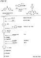
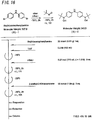
- the light-absorbing material shown by Structural Formula (6) above is manufactured by the process shown by [C22], [C23], and FIGS. 4 to 9 .
- the compound shown by Structural Formula (6)-1 and diethyl ether are agitated and mixed at -78°C, and tert-butyl lithium is added to the mixture, which is agitated and mixed for 2 hours at -78°C and then agitated and mixed for 1 hour at room temperature.
- 2-methyl-2-nitrosopropane is added to the resulting mixture, which is agitated and mixed for 2 hours at -78°C, and then agitated and mixed for 10 hours at room temperature to obtain the compound represented by Structural Formula (6)-2 (yield 40% to 50%).
- the compound represented by Structural Formula (6)-2, N,N-dimethylformamide (DMF), imidazole and tert-butyldimethylsilyl chloride are agitated and mixed for 10 hours at room temperature to obtain the compound represented by Structural Formula (6)-3 (yield 80% to 90%).
- the compound represented by Structural Formula (6)-3 and tetrahydrofuran are agitated and mixed at -78°C, the compound represented by Structural Formula (6)-a is added, and the mixture is agitated and mixed for 2 hours at -78°C and then agitated and mixed for 10 hours at room temperature.
- Monochloramine saturated solution, diethyl ether, tetrahydrofuran and 10% aqueous hydrochloric acid solution are added sequentially to the resulting mixture, and agitated and mixed for 10 minutes at room temperature to obtain the compound represented by Structural Formula (6)-4 (yield 50% to 60%).
- the compound represented by Structural Formula (6)-4, the compound represented by Structural Formula (6)-b, tris(dibenzylidenacetone) dipalladium (0), sodium tert-butoxide, tri tert-butylphosphine and toluene are mixed and refluxed overnight to obtain the compound represented by Structural Formula (6)-5 (yield 50% to 60%).
- the compound represented by Structural Formula (6)-5, the compound represented by Structural Formula (6)-c, ammonium acetate and acetic acid are mixed and refluxed for 3 hours to obtain the compound represented by Structural Formula (6)-6 (yield 80% to 90%).
- the compound represented by Structural Formula (6)-6, tetra-n-butylammonium fluoride (TBAF) and tetrahydrofuran are agitated and mixed for 5 hours at room temperature in an argon atmosphere, silver oxide is added, and the mixture is further agitated and mixed for 2 hours at room temperature in an argon atmosphere to obtain the compound represented by Structural Formula (6) (yield 95% to 100%) .
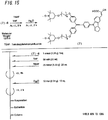
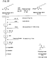
- the light-absorbing material represented by Structural Formula (7) above is manufactured by the process shown in [C28] and [C29], and FIGS. 10 to 15 .
- the compound represented by Structural Formula (7)-1, the compound represented by Structural Formula (7)-a, potassium carbonate and acetone are mixed, and refluxed overnight to obtain the compound represented by Structural Formula (7)-2 (yield 95% to 100%) .
- the compound represented by Structural Formula (7)-3 and tetrahydrofuran are agitated and mixed at -78°C.
- the compound represented by Structural Formula (7)-c is added to the resulting mixture, mixed for 2 hours at -78°C, and then agitated and mixed for 10 hours at room temperature.
- Monochloramine saturated solution, diethyl ether, tetrahydrofuran and 10% aqueous hydrochloride acid solution are added sequentially to the resulting mixture, which is then agitated and mixed for 10 minutes at room temperature to obtain the compound represented by Structural Formula (7)-4 below (yield 50% to 60%).
- the compound represented by Structural Formula (7)-4, the compound represented by Structural Formula (7)-d, tris(dibenzylidenacetone) dipalladium (0), sodium tert-butoxide, tri tert-butylphosphine and toluene are mixed and refluxed overnight to obtain the compound represented by Structural Formula (7)-5 below (yield 50% to 60%).
- the tetra-n-butylammonium fluoride represented by Structural Formula (7)-6 and tetrahydrofuran are agitated and mixed for 5 hours at room temperature in an argon atmosphere.
- Silver oxide is further added to the resulting mixture, which is then agitated and mixed for 2 hours at room temperature in an argon atmosphere to obtain the compound represented by Structural Formula (7) (yield 95% to 100%).
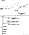
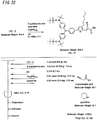
- the light-absorbing material represented by Structural Formula (8) is manufactured by the process shown in [C30] to [C33], and FIGS. 16 to 23 .
- the compound represented by Structural Formula (8)-1 and diethyl ether are agitated and mixed at -78°C.
- Tert-butyl lithium is added to the resulting mixture, which is then agitated and mixed for 2 hours at -78°C, and then agitated and mixed for 1 hour at room temperature.
- 2-methyl-2-nitrosopropane is added to this mixture, which is then agitated and mixed for 2 hours at -78°C and then agitated and mixed for 1 hour at room temperature to obtain the compound represented by Structural Formula (8)-2 (yield 40% to 50%).
- the compound represented by Structural Formula (8)-2, N,N-dimethylformamide, imidazole and tert-butyldimethylsilyl chloride are agitated and mixed for 10 hours at room temperature to obtain the compound represented by Structural Formula (8)-3 (yield 80% to 90%).
- the compound represented by Structural Formula (8)-4, carbon tetrachloride and N-bromosuccinimide are agitated and mixed for 5 hours at room temperature to obtain the compound represented by Structural Formula (8)-5 (yield 50% to 60%).
- the compound represented by Structural Formula (8)-5 and dimethyl ether are agitated and mixed at -78°C.
- Tert-butyl lithium is added to the resulting mixture, which is agitated and mixed for 2 hours at -78°C, and then agitated and mixed for 1 hour at room temperature.
- Triisopropyl borate is added to this mixture, which is agitated and mixed for 2 hours at -78°C, and then agitated and mixed for 10 hours at room temperature to obtain the compound represented by Structural Formula (8)-B (yield 40% to 50%).
- the compound represented by Structural Formula (8)-A, the compound represented by Structural Formula (8)-B, toluene, sodium tert-butoxide and tetra(triphenylphosphinato) palladium are mixed, and refluxed overnight in an argon atmosphere to obtain the compound represented by Structural Formula (8)-C.
- the compound represented by Structural Formula (8)-C, 2-cyanoacetic acid, acetonitrile (AN), piperidine and tetra(triphenylphosphinato) palladium are mixed, and refluxed for 5 hours in an argon atmosphere to obtain the compound represented by Structural Formula (8)-D (yield 80% to 90%).
- the compound represented by Structural Formula (8)-D, tetra-n-butyl ammonium fluoride and tetrahydrofuran are agitated and mixed for 5 hours at room temperature in an argon atmosphere.
- Silver oxide is added to the resulting mixture, which is then agitated and mixed for 2 hours at room temperature in an argon atmosphere to obtain the compound represented by Structural Formula (8) (yield 95% to 100%).
- the compound represented by Structural Formula (11) is manufactured by binding fine particles called quantum dots prepared by methods such as those described in Chemistry Letters 2007, Vol. 36, No. 6, page 712 to stable free radicals by methods such as those described in Journal of Molecular Catalysis A: Chemical, 1995, Vol. 101, p. 45 .
- a light-absorbing material having a radical part Y that acts as an electron receptor for light-absorbing site X is manufactured for example as shown below.
- the light-absorbing material represented by Structural Formula (14) is manufactured by the chemical reaction represented by [C34] below for example.
- the compound represented by Structural Formula (14)-1 and D131 dye are added to a mixed tetrahydrofuran (THF)/ethanol solvent, and the ester condensing agent 4-(4,6-dimethoxy)-1,3,5-triazine-2-yl)-4-methylmorpholinium chloride (DMT-MM) and a base (triethylamine; TEA) are added.
- the compound represented by Structural Formula (14)-2 is produced when the resulting solution is left for an hour at room temperature (yield 70%).
- the compound represented by Structural Formula (14)-2 is then added to ethanol, and an excess of iodomethane is further added. The resulting solution is left standing overnight at 60°C and then washed with water, and the product is re-precipitated with diethyl ether.
- the light-absorbing material represented by Structural Formula (14) is thus obtained as a reddish-brown solid (yield 65%).
- This light-absorbing material represented by Structural Formula (14) is soluble in chloroform, acetonitrile and methanol, and insoluble in water.
- the light-absorbing material represented by Structural Formula (14) is identified by 1H-NMR and FAB-Mass.
- the light-absorbing material represented by Structural Formula (15) is manufactured by the chemical reaction shown in [C35] below.
- the light-absorbing material represented by Structural Formula (16) is manufactured by the chemical reaction represented by [C36] below.
- the light-absorbing material represented by Structural Formula (17) is manufactured by the chemical reaction shown by [C37] below.
- the compound represented by Structural Formula (17)-1 is produced in a coupling reaction by lithiation of 4-(methoxycarbonyl)phenylboronic acid.
- PdCl 2 (PPh 3 ) 2 triethylamine, 4,4,5,5-tetramethyl and 1,3,2-dioxaborolane are then added to the compound represented by Structural Formula (17)-1, and the resulting mixture is agitated for 5 hours at 80°C in toluene in an inactive atmosphere.
- the compound represented by Structural Formula (17)-2 is then obtained as an orange powder by liquid separation and HPLC purification of this mixture.
- This compound represented by Structural Formula (17)-2 and MD-22 are added to a mixed benzene/water solvent, and Pd(PPh 3 ) 4 and K 2 CO 3 are further added to the resulting solution, which is then left standing for 12 hours at 50°C to produce a reaction (Suzuki coupling).
- the compound represented by Structural Formula (17)-3 is then obtained as a reddish-orange powder by liquid separation and HPLC purification of this solution.
- the light-absorbing material is applicable for example to a dye-sensitized or other photoelectric conversion elements such as a light-emitting element or solar cell.
- the photoelectric conversion element can comprise a charge transport material for transporting holes, a charge transport material for transporting electrons, a conductive substrate, and so forth for example.
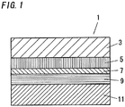
- FIG. 1 is a cross-section showing dye-sensitized solar cell 1 as one example of a photoelectric conversion element.
- this dye-sensitized solar cell 1 a layer formed of electron transport material 5 (electron transport layer), a layer formed of light-absorbing material 7, and a layer formed of charge transport material 9 (hole transport layer) are laminated between first substrate electrode 3 and second substrate electrode 11, which are disposed opposite each other.
- first substrate electrode 3 and second substrate electrode 11 has translucency.
- First substrate electrode 3 and second substrate electrode 11 have electrical conductivity for conducting charge outside the device.
- the substrate electrode having translucency may be transparent or non-transparent, but is preferably transparent in particular.
- first substrate electrode 3 is preferably formed of a material with translucency.
- First substrate electrode 3 may also comprise a base material formed from glass or a film or the like.
- first substrate electrode 3 has a conductive layer laminated on this base material for example.
- the conductive layer is laminated on the surface of the base material that faces electron transport material 5.
- the conductive layer is formed for example of indium or another metal; carbon; indium-tin composite oxide, antimony-doped tin oxide, fluorine-doped tin oxide or other conductive metal oxide; or a complex obtained by complexing these compounds.
- First substrate electrode 3 may also comprise a layer formed of a compound such as those described above, coated with a layer formed of silicon oxide, tin oxide, titanium oxide, zirconium oxide, aluminum oxide or the like.
- First substrate electrode 3 is formed by a dry process such as vapor deposition or sputtering, or a wet process such as dipping, spray thermal decomposition, CVD or the like.
- first substrate electrode 3 When light passes through second substrate electrode 11 to enter the photoelectric conversion element, first substrate electrode 3 may be provided with a film formed of titanium, nickel, zinc, stainless steel or other metal foil.
- Second substrate electrode 11 functions as the negative electrode of the photoelectric conversion element.
- Second substrate electrode 11 is formed only of metal for example.
- Second substrate electrode 11 may also comprise a film and a conductive layer laminated on this film. This conductive layer contacts the layer formed of charge transport material 9.
- the conductive layer in second substrate electrode 11 is formed of the same material as the conductive layer in first substrate electrode 3 for example.
- the conductive layer in second substrate electrode 11 is formed for example from a metal such as platinum, gold, silver, copper, aluminum, rhodium or indium; a carbon material such as graphite, carbon nanotubes or platinum-carrying carbon; a conductive metal oxide such as an indium-tin composite oxide, antimony-doped tin oxide, fluorine-doped tin oxide or the like; or a conductive polymer such as polyethylene dioxythiophene, polypyrrole, polyaniline or the like.
- charge transport material 9 is an electrolyte solution, it is particularly desirable that second substrate electrode 11 be formed of platinum, graphite, polyethylene dioxythiophene or the like.
- the surface resistance of first substrate electrode 3 and second substrate electrode 11 is preferably as low as possible.
- the surface resistance of first substrate electrode 3 and second substrate electrode 11 is preferably 200 ⁇ /sq. or less, or more preferably 50 ⁇ /sq. or less. There is no particular lower limit on the surface resistance of first substrate electrode 3 and second substrate electrode 11 but 0.1 ⁇ /sq. is normal.
- Light transmittance is preferably as high as possible in at least one of first substrate electrode 3 and second substrate electrode 11.
- the light transmittance of the substrate electrode with high light transmittance is preferably 50% or more, or more preferably 80% or more.
- the thicknesses of the conductive layers in first substrate electrode 3 and second substrate electrode 11 is preferably in the range of 0.1 ⁇ m to 10 ⁇ m. Within this range, it is easy to form a conductive layer with a uniform thickness, while maintaining the high light transmittance of the conductive layer.
- Electron transport material 5 is not limited as long as in which electrons are carriers.
- semiconductor materials that can be used as electron transport material 5 include oxides of Cd, Zn, In, Pb, Mo, W, Sb, Bi, Cu, Hg, Ti, Ag, Mn, Fe, V, Sn, Zr, Sr, Ga, Si, Cr and other metal elements; SrTiO 3 , CaTiO 3 and other metal oxides having perovskite structures; CdS, ZnS, In 2 S 3 , PbS, Mo 2 S, WS 2 , Sb 2 S 3 , Bi 2 S 3 , ZnCdS 2 , Cu 2 S and other sulfides, CdSe, In 2 Se 3 , WSe 2 , HgS, PbSe, CdTe and other metal chalcogenides; and GaAs, Si, Se, Cd 2 P 3 , Zn 2 P 3 , InP, AgBr, PbI 2 , HgI 2
- Electron transport material 5 may also be a complex containing at least one or more selected from semiconductor materials such as those described above.
- complexes include CdS/TiO 2 , CdS/AgI, Ag 2 S/AgI, CdS/ZnO, CdS/HgS, CdS/PbS, ZnO/ZnS, ZnO/ZnSe, CdS/HgS, CdS/CdSe, CdS/Te, CdSe/Te, ZnS/CdSe, ZnSe/CdSe, CdS/ZnS, TiO 2 /Cd 3 P 2 , CdS/CdSe/CdZnS, CdS/HgS/CdS and the like.
- Electron transport material 5 may also be C60 or a redox polymer having an oxidizing-reducing side chain or a polythiophene, polyaniline or other conductive polymer that can be made into an n-type semiconductor by doping.
- Electron transport material 5 may also be a polyradical compound that is an n-type semiconductor and has stable oxidative-reductive behavior, as disclosed in Japanese Patent Application Laid-open No. 2008-280400 .
- the molecular density of the light-absorbing material relative to the projected area of the photoelectric conversion element depends partly on the light-absorbing efficiency of light-absorbing material 7, but is preferably in the range of 1 ⁇ 10 -8 mol/cm 2 to 1 ⁇ 10 -6 mol/cm 2 from the standpoint of the output characteristics. If the density of light-absorbing material 7 is above this range, the amount of light-absorbing material 7 is too great relative to the amount of incident light, so that much of light-absorbing material 7 performs no function. If the density of light-absorbing material 7 is below this range, on the other hand, insufficient light will be absorbed by light-absorbing material 7.
- the photoelectric conversion element is an entirely translucent "see-through” type element, however, the density and absolute amount of light-absorbing material 7 may be reduced in accordance with the desired light transmittance of the photoelectric conversion element. Also, the photoelectric conversion efficiency of the photoelectric conversion element is improved when the layer formed of electron transport material 5 is a porous layer, and the ratio of effective area to projected area is 1 or more. The upper limit on the ratio of effective area to projected area is not particularly limited in the layer formed of electron transport material 5, but is preferably 1 million or less.
- Charge transport material (hole transport material) 9 may be a substance that produces redox pairs. Iodine (I - /I 3 - ) is often used as such a charge transport material 9, but this is not a limitation.
- charge transport material 9 may be a stably oxidized and reduced radical compound such as that described in Japanese Patent Application Laid-open No. 2003-100360 . This is desirable in particular because it promotes the reduction reaction of the oxidized radical site when radical site Y in light-absorbing material 7 is an electron donor, resulting in rapid reduction of radical site Y.
- Charge transport material 9 may also be an electrolyte solution.
- the solvent used to dissolve the electrolyte is preferably a compound with superior ion conductivity, capable of dissolving the component substances of the redox system.
- the solvent may be an aqueous solvent or organic solvent, but is preferably an organic solvent in order to further stabilize the components of the redox system in the electrolyte solution.
- organic solvent examples include dimethyl carbonate, diethyl carbonate, methylethyl carbonate, ethylene carbonate, propylene carbonate and other carbonate compounds; methyl acetate, methyl propionate, ⁇ -butyrolactone and other ester compounds; diethyl ether, 1,2-dimethoxyethane, 1,3-dioxosilane, tetrahydrofuran, 2-methyl-tetrahydrofuran and other ether compounds; 3-methyl-2-oxazolidinone, 2-methylpyrrolidone and other heterocyclic compounds; acetonitrile, methoxyacetonitrile, propionitrile and other nitrile compounds; and sulfolane, dimethyl sulfoxide, dimethyl formamide and other aprotic polar compounds and the like.
- One of these solvents can be used, or two or more may be combined. It is particularly desirable to use ethylene carbonate, propylene carbonate or another carbonate compound; ⁇ -butyrolactone, 3-methyl-2-oxazolidinone, 2-methylpyrrolidone or another heterocyclic compound; acetonitrile, methoxyacetonitrile, propionitrile, 3-methoxypropionitrile, valeric acid nitrile or another nitrile compound; or ethylene glycol, polyethylene glycol, polyethylene or another polyol compound or the like as the organic solvent.
- Charge transport material 9 may also be made into a gel by including an oil-gel system, a polyvinylidene fluoride polymer compound or other polymer matrix, a liquid crystal gel, an amino acid derivative or other low-molecular compound, or silica particles or other inorganic particles or the like.
- charge transport material 9 When charge transport material 9 contains a volatile component, it is effective to seal charge transport material 9. If it can become a p-type semiconductor when doped, charge transport material 9 may also be a conductive polymer such as polythiophene or polyaniline, or a polymer having easily oxidizable/reducible- side chains. In this case, liquid seepage is controlled because the layer formed of charge transport material 9 is a solid or gel, and therefore the photoelectric conversion efficiency of the photoelectric conversion element can be maintained at a high level long-term.
- a conductive polymer such as polythiophene or polyaniline
- a polymer having easily oxidizable/reducible- side chains In this case, liquid seepage is controlled because the layer formed of charge transport material 9 is a solid or gel, and therefore the photoelectric conversion efficiency of the photoelectric conversion element can be maintained at a high level long-term.
- the redox potential of radical site Y and the redox potential of the hole transport material or electron transport material are preferably adjusted so as to smoothly promote charge separation.
- radical site Y in the light-absorbing material 7 is an electron donor
- charge separation proceeds smoothly in light-absorbing material 7 if the redox potential of the hole transport material 9 is lower than the redox potential of radical site Y.
- radical site Y has a structure such as those given as examples in this Description, this potential adjustment can be achieved with relative ease by introducing functional groups into radical site Y or otherwise changing the molecular structure of radical site Y.
- radical site Y promotes an oxidation or reduction reaction of light-absorbing site X during the photoelectric conversion process that occurs when light-absorbing site X absorbs light, thereby causing rapid charge separation while controlling charge recombination. This enhances the photoelectric conversion of the photoelectric conversion element.
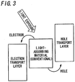
- radical site Y is an electron donor to light-absorbing site X
- FIG. 2(a) holes move from the excited light-absorbing site X to radical site Y during the photoelectric conversion process that occurs when light-absorbing site X absorbs light, thereby promoting a reduction reaction of light-absorbing site X.
- Radical site Y is oxidized by the movement of holes to radical site Y.
- radical site Y is reduced as holes move from radical site Y to the hole transport layer.
- electrons move from the reduced light-absorbing site X to the electron transport layer, oxidizing light-absorbing site X. This promotes charge separation while controlling charge recombination.
- radical site Y is an electron receptor for light-absorbing site X, as shown in FIG.
- FIG. 3 shows a conventional example.
- the light-absorbing material may have the same effect as a HALS (light stabilizer).
- HALS light stabilizer
- the undesirable radicals are eliminated, and deterioration of the light-absorbing material is prevented. This improves the durability of the photoelectric conversion element, allowing the superior characteristics of the photoelectric conversion element to be maintained long-term.
- the compound represented by Structural Formula (6)-2 (10 mmol (3.56 g) 1 eq), DMF (0.7 M (14.3 ml)), imidazole (30 mmol (2.10 g) 3 eq) and tert-butyldimethylsilyl chloride (12.5 mol (1.88 g) 1.25 eq) were agitated and mixed for 10 hours at room temperature to obtain the compound represented by Structural Formula (6)-3 (yield 80% to 90%).
- the compound represented by Structural Formula (6)-3 (5 mmol (2.92 g) 1 eq) and tetrahydrofuran (0.3 M (16.7 ml)) were agitated and mixed at -78°C
- the compound represented by Structural Formula (6)-a (15 mol (4.11 g) 1.5 eq) was added to the resulting solution and agitated and mixed for 2 hours at -78°C and 10 hours at room temperature
- the compound represented by Structural Formula (6)-4 (2 mmol (1.48 g) 1 eq) was mixed with the compound represented by Structural Formula (6)-b (3 mol (562 mg) 1.5 eq), tris(dibenzylidenacetone) dipalladium (0) (0.02 mol (18.0 mg) 0.01 eq), sodium tert-butoxide (3 mol (288 mg) 1.5 eq), tri tert-buylphosphine (0.06 mol (12 mg) 0.03 eq) and toluene (0.3 M (6.7 ml)), and the resulting solution was refluxed overnight to obtain the compound represented by Structural Formula (6)-5 (yield 50% to 60%).
- the compound represented by Structural Formula (6)-6 (1 mmol (911 mg) 1 eq), TBAF (20 mmol (5.23 g) 20 eq) and THF (50 mM (20 ml)) were agitated and mixed for 5 hours at room temperature in an argon atmosphere, and silver oxide (10 mol (2.31 g) 10 eq) was added to the resulting solution and agitated and mixed for 2 hours at room temperature in an argon atmosphere to obtain the compound represented by Structural Formula (6) (yield 95% to 100%).
- the compound represented by Structural Formula (7)-1 (0.1 mol (28.8 g) 1 eq), the compound represented by Structural Formula (7)-a (0.125 mol (36.4 g) 1.25 eq), potassium carbonate (0.15 mol (20.7 g) 1.5 eq) and acetone (0.7 M (142 ml)) were mixed, and the resulting solution was refluxed overnight to obtain the compound represented by Structural Formula (7)-2 (yield 95% to 100%).
- the compound represented by Structural Formula (7)-2 (0.1 mol (45.1 g) 1 eq), the compound represented by Structural Formula (7)-b (0.04 mol (8.59 g) 0.4 eq), sodium hydroxide (0.3 mol (41.4 g) 3 eq) and acetone (0.7 M (142 ml)) were mixed, and the resulting solution was refluxed overnight to obtain the compound represented by Structural Formula (7)-3 (yield 95% to 100%).
- the compound represented by Structural Formula (7)-3 (5 mmol (4.77 g) 1 eq) and tetrahydrofuran (0.3 M (16.7 ml)) were agitated and mixed at -78°C
- the compound represented by Structural Formula (7)-c (15 mol (4.11 g) 1.5 eq) was further added to the resulting solution and mixed for 2 hours at -78°C, and this solution was agitated and mixed for 10 hours at room temperature, after which monochloramine saturated solution (2 ml), diethyl ether (50 ml), tetrahydrofuran (50 ml) and 10% aqueous hydrochloric acid solution (20 ml) were added to this solution and agitated and mixed for 10 minutes at room temperature to obtain the compound represented by Structural Formula (7)-4 (yield 50% to 60%) .
- the compound represented by Structural Formula (7)-4 (2 mmol (2.21 g) 1 eq), the compound represented by Structural Formula (7)-d (3 mol (562 mg) 1.5 eq), tris(dibenzylidenacetone) dipalladium (0) (0.02 mol (18.0 mg) 0.01 eq), sodium tert-butoxide (3 mol (288 mg) 1.5 eq), tri tert-butylphosphine (0.06 mol (12 mg) 0.03 eq) and toluene (0.3 M (6.7 ml)) were mixed, and the resulting solution was refluxed overnight to obtain the compound represented by Structural Formula (7)-5 (yield 50% to 60%).
- the compound represented by Structural Formula (7)-6 (1 mmol (1.28 g) 1 eq), TBAF (20 mmol (5.23 g) 20 eq) and THF (50 mM (20 ml)) were agitated and mixed for 5 hours at room temperature in an argon atmosphere, and silver oxide (10 mol (2.31 g) 10 eq) was added and agitated and mixed for 2 hours at room temperature in an argon atmosphere to obtain the compound represented by Structural Formula (7) (yield 95% to 100%) .
- the compound represented by Structural Formula (8)-2 (10 mmol (5.72 g) 1 eq), DMF (0.7 M (14.3 ml)), imidazole (30 mmol (2.10 g) 3 eq) and tert-butyldimethylsilyl chloride (12.5 mol (1.88 g) 1.25 eq) were agitated and mixed for 10 hours at room temperature to obtain the compound represented by Structural Formula (8)-3 (yield 80% to 90%).
- the compound represented by Structural Formula (8)-3 (10 mmol (5.72 g) 1 eq), toluene (0.7 M (14.3 ml)), sodium tert-butoxide (12.5 mol (1.20 g) 1.25 eq), copper iodide (1 mmol (0.19 g) 0.1 eq) and piperidine (1.0 mol (85 mg) 0.01 eq) were agitated and mixed, and the resulting solution was refluxed for 5 hours in an argon atmosphere to obtain the compound represented by Structural Formula (8)-A (yield 50% to 60%) .
- the compound represented by Structural Formula (8)-4 (0.1 mol (16.8 g) 1 eq), carbon tetrachloride (1 M (100 ml)) and N-bromosuccinimide (0.1 mol (17.8 g) 1 eq) were agitated and mixed for 3 hours at room temperature to obtain the compound represented by Structural Formula (8)-5 (yield 50% to 60%).
- the compound represented by Structural Formula (8)-D (1 mmol (909 mg) 1 eq), TBAF (20 mmol (5.23 g) 20 eq) and THF (50 mM (20 ml)) were agitated and mixed for 5 hours at room temperature in an argon atmosphere, and silver oxide (10 mol (2.31 g) 10 eq) was added to the resulting solution and agitated and mixed for 2 hours at room temperature in an argon atmosphere to obtain the compound represented by Structural Formula (8) (yield 95% to 100%).
- High-purity titanium oxide powder with an average primary particle diameter of 20 nm was dispersed in ethyl cellulose to obtain a paste for screen printing.
- a 10 nm-thick titanium oxide film was formed by sputtering on a 1 mm-thick conductive glass substrate (fluorine-doped tin oxide, surface resistance 100 ⁇ /sq.) to prepare a first substrate electrode.
- the aforementioned paste for screen printing was coated on this first substrate electrode, and dried to form a dry coating. This dry coating was baked for 30 minutes in air at 500°C.
- a 1.5 ⁇ m-thick porous titanium oxide film was formed in this way on the first substrate electrode.
- a titanium tetrachloride aqueous solution with a concentration of 0.04 mol/dm 3 was coated on this porous titanium oxide film, the porous titanium oxide film was heated for 30 minutes at 70°C, and this porous titanium oxide film was then rinsed with distilled water and air dried. An electron transport layer was thus formed on the first substrate electrode.
- a dimethyl formamide solution containing the light-absorbing material represented by Structural Formula (6), a dimethyl formamide solution containing the light-absorbing material represented by Structural Formula (7), and a dimethyl formamide solution containing the light-absorbing material represented by Structural Formula (8) were each prepared.
- the concentration of the light-absorbing material in each solution was 0.2 mM.
- the electron transport layer was immersed together with the first substrate electrode in the dimethylformamide solution containing the light-absorbing material, and the electron transport layer together with the first substrate electrode was left in this state in a dark place for 24 hours at room temperature. This electron transport layer was then washed with solvent.
- a platinum film was formed by thermal reduction of chloroplatinic acid on the surface of a conductive glass substrate (Nippon Sheet Glass Company, fluorine-doped SnO 2 , surface resistance 10 ⁇ /sq.) to obtain the second substrate electrode.
- the first substrate electrode and second substrate electrode were arranged facing each other with the electron transport layer between the two.
- a seal material hot-melt adhesive, Mitsui-DuPont Polychemical, BynelTM
- the first substrate electrode and second substrate electrode were pressed together in this state with heat to affix the two together via the seal material.
- a first substrate electrode was prepared by forming a layer of fluorine-doped SnO 2 on a 1 mm-thick conductive glass substrate (Asahi Glass, surface resistance 10 ⁇ /sq.).
- a platinum plate was prepared as the second substrate electrode.
- This second substrate electrode and the first substrate electrode were arranged facing each other with the film of light-absorbing material between the two, and with the space between the two surrounded by seal material.
- the first substrate electrode and second substrate electrode were heated and pressed to affix the two together via the seal material.
- the open voltage of this photoelectric conversion element under light irradiation was 480 mV, and when the light was blocked the output voltage gradually converged to 0 mV. When this was again exposed to light, the open circuit voltage converged to 480 mV. This optical response behavior was stable with repeated use.
- the light-absorbing material represented by Structural Formula (15), the light-absorbing material represented by Structural Formula (16) and the light-absorbing material represented by Structural Formula (17) were used in place of the light absorbing material represented by Structural Formula (14) in Example 5, Example 6 and Example 7, respectively.
- photoelectric conversion elements were prepared by the same methods and under the same conditions as in Example 4.
- Example 4 When the open voltages of these photoelectric conversion elements were measured as in Example 4, the result was 430 mV in Example 5, 410 mV in Example 6 and 380 mV in Example 7, and the optical response behavior was stable with repeated use as in Example 4.
- Example 4 5 mg of Mitsubishi Paper Mills D131 dye and 5 mg of viologen were dissolved in 5 ml of N,N-dimethylformamide, and the resulting solution was applied by drop casting to a first substrate electrode to form a film 50 nm thick. No film of light-absorbing material was formed as in Example 4. A photoelectric conversion element was then prepared under the same conditions as in Example 4.
- the open voltage of this photoelectric conversion element under light exposure was 90 mV, and when the light was blocked the output voltage gradually converged to 0 mV. When light exposure was resumed, the open voltage converged to 90 mV. This optical response behavior was stable with repeated use.
- Example 4 5 mg of Mitsubishi Paper Mills D131 dye and 5 mg of galvinoxyl were dissolved in 5 ml of N,N-dimethylformamide, and the resulting solution was applied by drop casting to a first substrate electrode to form a film 50 nm thick. No film of light-absorbing material was formed as in Example 4. A photoelectric conversion element was then prepared under the same conditions as in Example 4.
- the open voltage of this photoelectric conversion element under light exposure was 40 mV, and when the light was blocked the output voltage gradually converged to 0 mV. When light exposure was resumed, the open voltage converged to 40 mV. This optical response behavior was stable with repeated use.
Landscapes
- Chemical & Material Sciences (AREA)
- Organic Chemistry (AREA)
- Engineering & Computer Science (AREA)
- Materials Engineering (AREA)
- Spectroscopy & Molecular Physics (AREA)
- Physics & Mathematics (AREA)
- Chemical Kinetics & Catalysis (AREA)
- Power Engineering (AREA)
- Electrochemistry (AREA)
- General Chemical & Material Sciences (AREA)
- Microelectronics & Electronic Packaging (AREA)
- Photovoltaic Devices (AREA)
- Hybrid Cells (AREA)
Applications Claiming Priority (2)
| Application Number | Priority Date | Filing Date | Title |
|---|---|---|---|
| JP2009124522 | 2009-05-22 | ||
| PCT/JP2010/058662 WO2010134607A1 (ja) | 2009-05-22 | 2010-05-21 | 光吸収材料及び光電変換素子 |
Publications (3)
| Publication Number | Publication Date |
|---|---|
| EP2433989A1 EP2433989A1 (en) | 2012-03-28 |
| EP2433989A4 EP2433989A4 (en) | 2014-04-02 |
| EP2433989B1 true EP2433989B1 (en) | 2018-03-14 |
Family
ID=43126284
Family Applications (1)
| Application Number | Title | Priority Date | Filing Date |
|---|---|---|---|
| EP10777838.3A Active EP2433989B1 (en) | 2009-05-22 | 2010-05-21 | Light-absorbing material and photoelectric conversion element |
Country Status (7)
| Country | Link |
|---|---|
| US (1) | US8729532B2 (enExample) |
| EP (1) | EP2433989B1 (enExample) |
| JP (1) | JP5711470B2 (enExample) |
| KR (1) | KR101366122B1 (enExample) |
| CN (1) | CN102439092B (enExample) |
| TW (1) | TW201107457A (enExample) |
| WO (1) | WO2010134607A1 (enExample) |
Families Citing this family (17)
| Publication number | Priority date | Publication date | Assignee | Title |
|---|---|---|---|---|
| WO2012061870A1 (en) * | 2010-11-08 | 2012-05-18 | Monash University | Method and system for catalysis |
| JP2012190666A (ja) * | 2011-03-10 | 2012-10-04 | Panasonic Corp | 光吸収材料及び光電変換素子 |
| JP5996255B2 (ja) * | 2011-05-09 | 2016-09-21 | 旭化成株式会社 | 光電変換素子及びπ共役型有機ラジカル化合物 |
| US8952372B2 (en) | 2011-12-28 | 2015-02-10 | Panasonic Corporation | Photoelectric element and method for producing the same |
| JP5957012B2 (ja) | 2011-12-28 | 2016-07-27 | パナソニック株式会社 | 光電気素子 |
| TWI470776B (zh) * | 2011-12-29 | 2015-01-21 | Ind Tech Res Inst | 光偵測陣列結構與光偵測模組 |
| EP2828894A1 (en) * | 2012-03-22 | 2015-01-28 | The University Of Manchester | Photovoltaic cells |
| CN104797644A (zh) * | 2012-12-03 | 2015-07-22 | 阿克伦大学 | 具有宽带响应和增加的光电响应度的有机聚合物光电装置 |
| JP6239338B2 (ja) * | 2013-10-11 | 2017-11-29 | 三菱製紙株式会社 | 有機色素 |
| US9368288B2 (en) * | 2013-10-11 | 2016-06-14 | Panasonic Corporation | Photoelectric conversion element |
| CN104112787B (zh) * | 2014-07-28 | 2016-04-13 | 武汉鑫神光电科技有限公司 | 一种硫化银/钙钛矿体异质结太阳能电池及其制备方法 |
| JP6743812B2 (ja) * | 2015-05-12 | 2020-08-19 | 住友化学株式会社 | 有機光電変換素子 |
| WO2017043871A1 (ko) * | 2015-09-07 | 2017-03-16 | 주식회사 레이언스 | X선 디텍터 |
| KR20170029370A (ko) | 2015-09-07 | 2017-03-15 | 주식회사 레이언스 | X선 디텍터 |
| CN113130769B (zh) * | 2021-04-09 | 2023-10-13 | 东南大学 | 二维层状钙钛矿单晶、宽光谱光电探测器及其制备方法 |
| JP7294601B2 (ja) * | 2021-07-13 | 2023-06-20 | 独立行政法人国立高等専門学校機構 | 光電変換素子の製造方法、光電変換素子、光電変換素子におけるn型半導体層の製造方法 |
| CN115295747B (zh) * | 2022-07-29 | 2025-09-05 | 合肥工业大学 | 基于激基复合物的多量子阱结构改善oled器件性能的方法 |
Citations (2)
| Publication number | Priority date | Publication date | Assignee | Title |
|---|---|---|---|---|
| EP1981118A1 (en) * | 2006-02-02 | 2008-10-15 | Sony Corporation | Dye sensitization photoelectric converter |
| EP2009064A2 (en) * | 2002-07-29 | 2008-12-31 | Mitsubishi Paper Mills Limited | Organic dye, photoelectric transducing material, semiconductor electrode, and photoelectric transducing device |
Family Cites Families (10)
| Publication number | Priority date | Publication date | Assignee | Title |
|---|---|---|---|---|
| CH674596A5 (enExample) | 1988-02-12 | 1990-06-15 | Sulzer Ag | |
| JP3687736B2 (ja) | 2000-02-25 | 2005-08-24 | 日本電気株式会社 | 二次電池 |
| JP4967211B2 (ja) | 2001-09-26 | 2012-07-04 | 日本電気株式会社 | 光電気化学デバイス |
| JP4080288B2 (ja) | 2002-09-26 | 2008-04-23 | 三菱製紙株式会社 | 太陽電池用メロシアニン色素 |
| CN101416345B (zh) * | 2006-02-02 | 2012-09-26 | 索尼株式会社 | 染料敏化光电转换装置 |
| JP2007262263A (ja) * | 2006-03-29 | 2007-10-11 | Fujifilm Corp | フタロシアニン化合物 |
| JP2008201912A (ja) * | 2007-02-20 | 2008-09-04 | Fujifilm Corp | 光重合性組成物 |
| JP5176129B2 (ja) | 2007-05-09 | 2013-04-03 | 日本電気株式会社 | ポリラジカル化合物および電池 |
| JP5237664B2 (ja) * | 2007-06-14 | 2013-07-17 | パナソニック株式会社 | 光電変換素子 |
| JP5023866B2 (ja) | 2007-07-27 | 2012-09-12 | ソニー株式会社 | 色素増感光電変換素子およびその製造方法ならびに電子機器 |
-
2010
- 2010-05-21 JP JP2010117398A patent/JP5711470B2/ja active Active
- 2010-05-21 TW TW099116307A patent/TW201107457A/zh unknown
- 2010-05-21 CN CN201080022143.2A patent/CN102439092B/zh active Active
- 2010-05-21 EP EP10777838.3A patent/EP2433989B1/en active Active
- 2010-05-21 WO PCT/JP2010/058662 patent/WO2010134607A1/ja not_active Ceased
- 2010-05-21 KR KR1020117030731A patent/KR101366122B1/ko active Active
- 2010-05-21 US US13/322,048 patent/US8729532B2/en active Active
Patent Citations (2)
| Publication number | Priority date | Publication date | Assignee | Title |
|---|---|---|---|---|
| EP2009064A2 (en) * | 2002-07-29 | 2008-12-31 | Mitsubishi Paper Mills Limited | Organic dye, photoelectric transducing material, semiconductor electrode, and photoelectric transducing device |
| EP1981118A1 (en) * | 2006-02-02 | 2008-10-15 | Sony Corporation | Dye sensitization photoelectric converter |
Also Published As
| Publication number | Publication date |
|---|---|
| KR101366122B1 (ko) | 2014-02-25 |
| EP2433989A1 (en) | 2012-03-28 |
| US8729532B2 (en) | 2014-05-20 |
| CN102439092A (zh) | 2012-05-02 |
| WO2010134607A1 (ja) | 2010-11-25 |
| CN102439092B (zh) | 2014-10-08 |
| JP2011006665A (ja) | 2011-01-13 |
| EP2433989A4 (en) | 2014-04-02 |
| JP5711470B2 (ja) | 2015-04-30 |
| US20120181516A1 (en) | 2012-07-19 |
| TW201107457A (en) | 2011-03-01 |
| KR20120023124A (ko) | 2012-03-12 |
Similar Documents
| Publication | Publication Date | Title |
|---|---|---|
| EP2433989B1 (en) | Light-absorbing material and photoelectric conversion element | |
| JP5204848B2 (ja) | 光電気素子 | |
| Zafer et al. | Characterization of N, N′-bis-2-(1-hydoxy-4-methylpentyl)-3, 4, 9, 10-perylene bis (dicarboximide) sensitized nanocrystalline TiO2 solar cells with polythiophene hole conductors | |
| Maeda et al. | Intramolecular exciton-coupled squaraine dyes for dye-sensitized solar cells | |
| EP2259377A1 (en) | Photosensitizing element and solar battery using the photosensitizing element | |
| US20080178933A1 (en) | Photoelectric conversion element and solar cell | |
| Chen et al. | New ruthenium sensitizer with carbazole antennas for efficient and stable thin-film dye-sensitized solar cells | |
| EP2596509B1 (en) | Dye solar cell with improved stability | |
| JP2001273937A (ja) | 光電変換素子および光電池 | |
| JP2008021496A (ja) | 色素増感光電変換素子 | |
| Nwanya et al. | Dyed sensitized solar cells: A technically and economically alternative concept to pn junction photovoltaic devices. | |
| CN103503099B (zh) | 光电元件 | |
| JP5584447B2 (ja) | 光電気素子 | |
| JP2014186995A (ja) | 透明色素増感太陽電池および色素増感太陽電池モジュール | |
| EP2386607A2 (en) | Novel organic dye containing trialkoxysilyl group and method for preparing same | |
| WO2012121192A1 (ja) | 光吸収材料及び光電変換素子 | |
| Beni et al. | Synthesis and characterization of new triphenylamine-based dyes with novel anchoring groups for dye-sensitized solar cell applications | |
| JP2008226582A (ja) | 光電変換素子及び太陽電池 | |
| JP4295954B2 (ja) | 色素増感太陽電池 | |
| JP5250989B2 (ja) | 光電変換素子及び太陽電池 | |
| KR20130081000A (ko) | 플루오렌 유도체 및 그의 염 | |
| JP2013055060A (ja) | 光電変換素子及び太陽電池 |
Legal Events
| Date | Code | Title | Description |
|---|---|---|---|
| PUAI | Public reference made under article 153(3) epc to a published international application that has entered the european phase |
Free format text: ORIGINAL CODE: 0009012 |
|
| 17P | Request for examination filed |
Effective date: 20111209 |
|
| AK | Designated contracting states |
Kind code of ref document: A1 Designated state(s): AL AT BE BG CH CY CZ DE DK EE ES FI FR GB GR HR HU IE IS IT LI LT LU LV MC MK MT NL NO PL PT RO SE SI SK SM TR |
|
| RIN1 | Information on inventor provided before grant (corrected) |
Inventor name: OYAIZU, KENICHI Inventor name: KATO, FUMIAKI Inventor name: KAMBE, SHINGO Inventor name: SEKIGUCHI, TAKASHI Inventor name: SUZUKA, MICHIO Inventor name: YAMAKI, TAKEYUKI Inventor name: NISHIDE, HIROYUKI |
|
| DAX | Request for extension of the european patent (deleted) | ||
| A4 | Supplementary search report drawn up and despatched |
Effective date: 20140228 |
|
| RIC1 | Information provided on ipc code assigned before grant |
Ipc: H01M 14/00 20060101ALI20140224BHEP Ipc: C09B 69/00 20060101AFI20140224BHEP Ipc: H01L 31/04 20140101ALI20140224BHEP Ipc: C09B 47/00 20060101ALI20140224BHEP Ipc: C09B 57/00 20060101ALI20140224BHEP Ipc: C09B 57/10 20060101ALI20140224BHEP |
|
| 17Q | First examination report despatched |
Effective date: 20160316 |
|
| GRAP | Despatch of communication of intention to grant a patent |
Free format text: ORIGINAL CODE: EPIDOSNIGR1 |
|
| INTG | Intention to grant announced |
Effective date: 20171004 |
|
| GRAS | Grant fee paid |
Free format text: ORIGINAL CODE: EPIDOSNIGR3 |
|
| GRAA | (expected) grant |
Free format text: ORIGINAL CODE: 0009210 |
|
| AK | Designated contracting states |
Kind code of ref document: B1 Designated state(s): AL AT BE BG CH CY CZ DE DK EE ES FI FR GB GR HR HU IE IS IT LI LT LU LV MC MK MT NL NO PL PT RO SE SI SK SM TR |
|
| REG | Reference to a national code |
Ref country code: GB Ref legal event code: FG4D |
|
| REG | Reference to a national code |
Ref country code: CH Ref legal event code: EP Ref country code: AT Ref legal event code: REF Ref document number: 978841 Country of ref document: AT Kind code of ref document: T Effective date: 20180315 |
|
| REG | Reference to a national code |
Ref country code: IE Ref legal event code: FG4D |
|
| REG | Reference to a national code |
Ref country code: DE Ref legal event code: R096 Ref document number: 602010049187 Country of ref document: DE |
|
| REG | Reference to a national code |
Ref country code: NL Ref legal event code: MP Effective date: 20180314 |
|
| REG | Reference to a national code |
Ref country code: LT Ref legal event code: MG4D |
|
| PG25 | Lapsed in a contracting state [announced via postgrant information from national office to epo] |
Ref country code: FI Free format text: LAPSE BECAUSE OF FAILURE TO SUBMIT A TRANSLATION OF THE DESCRIPTION OR TO PAY THE FEE WITHIN THE PRESCRIBED TIME-LIMIT Effective date: 20180314 Ref country code: NO Free format text: LAPSE BECAUSE OF FAILURE TO SUBMIT A TRANSLATION OF THE DESCRIPTION OR TO PAY THE FEE WITHIN THE PRESCRIBED TIME-LIMIT Effective date: 20180614 Ref country code: HR Free format text: LAPSE BECAUSE OF FAILURE TO SUBMIT A TRANSLATION OF THE DESCRIPTION OR TO PAY THE FEE WITHIN THE PRESCRIBED TIME-LIMIT Effective date: 20180314 Ref country code: CY Free format text: LAPSE BECAUSE OF FAILURE TO SUBMIT A TRANSLATION OF THE DESCRIPTION OR TO PAY THE FEE WITHIN THE PRESCRIBED TIME-LIMIT Effective date: 20180314 Ref country code: LT Free format text: LAPSE BECAUSE OF FAILURE TO SUBMIT A TRANSLATION OF THE DESCRIPTION OR TO PAY THE FEE WITHIN THE PRESCRIBED TIME-LIMIT Effective date: 20180314 Ref country code: ES Free format text: LAPSE BECAUSE OF FAILURE TO SUBMIT A TRANSLATION OF THE DESCRIPTION OR TO PAY THE FEE WITHIN THE PRESCRIBED TIME-LIMIT Effective date: 20180314 |
|
| REG | Reference to a national code |
Ref country code: AT Ref legal event code: MK05 Ref document number: 978841 Country of ref document: AT Kind code of ref document: T Effective date: 20180314 |
|
| PG25 | Lapsed in a contracting state [announced via postgrant information from national office to epo] |
Ref country code: GR Free format text: LAPSE BECAUSE OF FAILURE TO SUBMIT A TRANSLATION OF THE DESCRIPTION OR TO PAY THE FEE WITHIN THE PRESCRIBED TIME-LIMIT Effective date: 20180615 Ref country code: SE Free format text: LAPSE BECAUSE OF FAILURE TO SUBMIT A TRANSLATION OF THE DESCRIPTION OR TO PAY THE FEE WITHIN THE PRESCRIBED TIME-LIMIT Effective date: 20180314 Ref country code: LV Free format text: LAPSE BECAUSE OF FAILURE TO SUBMIT A TRANSLATION OF THE DESCRIPTION OR TO PAY THE FEE WITHIN THE PRESCRIBED TIME-LIMIT Effective date: 20180314 Ref country code: BG Free format text: LAPSE BECAUSE OF FAILURE TO SUBMIT A TRANSLATION OF THE DESCRIPTION OR TO PAY THE FEE WITHIN THE PRESCRIBED TIME-LIMIT Effective date: 20180614 |
|
| PG25 | Lapsed in a contracting state [announced via postgrant information from national office to epo] |
Ref country code: NL Free format text: LAPSE BECAUSE OF FAILURE TO SUBMIT A TRANSLATION OF THE DESCRIPTION OR TO PAY THE FEE WITHIN THE PRESCRIBED TIME-LIMIT Effective date: 20180314 Ref country code: AL Free format text: LAPSE BECAUSE OF FAILURE TO SUBMIT A TRANSLATION OF THE DESCRIPTION OR TO PAY THE FEE WITHIN THE PRESCRIBED TIME-LIMIT Effective date: 20180314 Ref country code: PL Free format text: LAPSE BECAUSE OF FAILURE TO SUBMIT A TRANSLATION OF THE DESCRIPTION OR TO PAY THE FEE WITHIN THE PRESCRIBED TIME-LIMIT Effective date: 20180314 Ref country code: IT Free format text: LAPSE BECAUSE OF FAILURE TO SUBMIT A TRANSLATION OF THE DESCRIPTION OR TO PAY THE FEE WITHIN THE PRESCRIBED TIME-LIMIT Effective date: 20180314 Ref country code: RO Free format text: LAPSE BECAUSE OF FAILURE TO SUBMIT A TRANSLATION OF THE DESCRIPTION OR TO PAY THE FEE WITHIN THE PRESCRIBED TIME-LIMIT Effective date: 20180314 Ref country code: EE Free format text: LAPSE BECAUSE OF FAILURE TO SUBMIT A TRANSLATION OF THE DESCRIPTION OR TO PAY THE FEE WITHIN THE PRESCRIBED TIME-LIMIT Effective date: 20180314 |
|
| PG25 | Lapsed in a contracting state [announced via postgrant information from national office to epo] |
Ref country code: CZ Free format text: LAPSE BECAUSE OF FAILURE TO SUBMIT A TRANSLATION OF THE DESCRIPTION OR TO PAY THE FEE WITHIN THE PRESCRIBED TIME-LIMIT Effective date: 20180314 Ref country code: SM Free format text: LAPSE BECAUSE OF FAILURE TO SUBMIT A TRANSLATION OF THE DESCRIPTION OR TO PAY THE FEE WITHIN THE PRESCRIBED TIME-LIMIT Effective date: 20180314 Ref country code: AT Free format text: LAPSE BECAUSE OF FAILURE TO SUBMIT A TRANSLATION OF THE DESCRIPTION OR TO PAY THE FEE WITHIN THE PRESCRIBED TIME-LIMIT Effective date: 20180314 Ref country code: SK Free format text: LAPSE BECAUSE OF FAILURE TO SUBMIT A TRANSLATION OF THE DESCRIPTION OR TO PAY THE FEE WITHIN THE PRESCRIBED TIME-LIMIT Effective date: 20180314 |
|
| REG | Reference to a national code |
Ref country code: CH Ref legal event code: PL |
|
| REG | Reference to a national code |
Ref country code: DE Ref legal event code: R097 Ref document number: 602010049187 Country of ref document: DE |
|
| PG25 | Lapsed in a contracting state [announced via postgrant information from national office to epo] |
Ref country code: PT Free format text: LAPSE BECAUSE OF FAILURE TO SUBMIT A TRANSLATION OF THE DESCRIPTION OR TO PAY THE FEE WITHIN THE PRESCRIBED TIME-LIMIT Effective date: 20180716 |
|
| PLBE | No opposition filed within time limit |
Free format text: ORIGINAL CODE: 0009261 |
|
| STAA | Information on the status of an ep patent application or granted ep patent |
Free format text: STATUS: NO OPPOSITION FILED WITHIN TIME LIMIT |
|
| REG | Reference to a national code |
Ref country code: BE Ref legal event code: MM Effective date: 20180531 |
|
| PG25 | Lapsed in a contracting state [announced via postgrant information from national office to epo] |
Ref country code: MC Free format text: LAPSE BECAUSE OF FAILURE TO SUBMIT A TRANSLATION OF THE DESCRIPTION OR TO PAY THE FEE WITHIN THE PRESCRIBED TIME-LIMIT Effective date: 20180314 Ref country code: DK Free format text: LAPSE BECAUSE OF FAILURE TO SUBMIT A TRANSLATION OF THE DESCRIPTION OR TO PAY THE FEE WITHIN THE PRESCRIBED TIME-LIMIT Effective date: 20180314 |
|
| 26N | No opposition filed |
Effective date: 20181217 |
|
| REG | Reference to a national code |
Ref country code: IE Ref legal event code: MM4A |
|
| GBPC | Gb: european patent ceased through non-payment of renewal fee |
Effective date: 20180614 |
|
| PG25 | Lapsed in a contracting state [announced via postgrant information from national office to epo] |
Ref country code: SI Free format text: LAPSE BECAUSE OF FAILURE TO SUBMIT A TRANSLATION OF THE DESCRIPTION OR TO PAY THE FEE WITHIN THE PRESCRIBED TIME-LIMIT Effective date: 20180314 Ref country code: LI Free format text: LAPSE BECAUSE OF NON-PAYMENT OF DUE FEES Effective date: 20180531 Ref country code: CH Free format text: LAPSE BECAUSE OF NON-PAYMENT OF DUE FEES Effective date: 20180531 |
|
| PG25 | Lapsed in a contracting state [announced via postgrant information from national office to epo] |
Ref country code: LU Free format text: LAPSE BECAUSE OF NON-PAYMENT OF DUE FEES Effective date: 20180521 |
|
| PG25 | Lapsed in a contracting state [announced via postgrant information from national office to epo] |
Ref country code: FR Free format text: LAPSE BECAUSE OF NON-PAYMENT OF DUE FEES Effective date: 20180531 Ref country code: GB Free format text: LAPSE BECAUSE OF NON-PAYMENT OF DUE FEES Effective date: 20180614 Ref country code: IE Free format text: LAPSE BECAUSE OF NON-PAYMENT OF DUE FEES Effective date: 20180521 |
|
| PG25 | Lapsed in a contracting state [announced via postgrant information from national office to epo] |
Ref country code: BE Free format text: LAPSE BECAUSE OF NON-PAYMENT OF DUE FEES Effective date: 20180531 |
|
| PG25 | Lapsed in a contracting state [announced via postgrant information from national office to epo] |
Ref country code: MT Free format text: LAPSE BECAUSE OF NON-PAYMENT OF DUE FEES Effective date: 20180521 |
|
| PG25 | Lapsed in a contracting state [announced via postgrant information from national office to epo] |
Ref country code: TR Free format text: LAPSE BECAUSE OF FAILURE TO SUBMIT A TRANSLATION OF THE DESCRIPTION OR TO PAY THE FEE WITHIN THE PRESCRIBED TIME-LIMIT Effective date: 20180314 |
|
| PG25 | Lapsed in a contracting state [announced via postgrant information from national office to epo] |
Ref country code: HU Free format text: LAPSE BECAUSE OF FAILURE TO SUBMIT A TRANSLATION OF THE DESCRIPTION OR TO PAY THE FEE WITHIN THE PRESCRIBED TIME-LIMIT; INVALID AB INITIO Effective date: 20100521 |
|
| PG25 | Lapsed in a contracting state [announced via postgrant information from national office to epo] |
Ref country code: MK Free format text: LAPSE BECAUSE OF NON-PAYMENT OF DUE FEES Effective date: 20180314 |
|
| PG25 | Lapsed in a contracting state [announced via postgrant information from national office to epo] |
Ref country code: IS Free format text: LAPSE BECAUSE OF FAILURE TO SUBMIT A TRANSLATION OF THE DESCRIPTION OR TO PAY THE FEE WITHIN THE PRESCRIBED TIME-LIMIT Effective date: 20180714 |
|
| PGFP | Annual fee paid to national office [announced via postgrant information from national office to epo] |
Ref country code: DE Payment date: 20250325 Year of fee payment: 16 |