WO2010134264A1 - 半導体集積回路の設計装置、そのデータ処理方法、およびその制御プログラム - Google Patents
半導体集積回路の設計装置、そのデータ処理方法、およびその制御プログラム Download PDFInfo
- Publication number
- WO2010134264A1 WO2010134264A1 PCT/JP2010/002881 JP2010002881W WO2010134264A1 WO 2010134264 A1 WO2010134264 A1 WO 2010134264A1 JP 2010002881 W JP2010002881 W JP 2010002881W WO 2010134264 A1 WO2010134264 A1 WO 2010134264A1
- Authority
- WO
- WIPO (PCT)
- Prior art keywords
- semiconductor integrated
- integrated circuit
- noise
- timing
- delay analysis
- Prior art date
- Legal status (The legal status is an assumption and is not a legal conclusion. Google has not performed a legal analysis and makes no representation as to the accuracy of the status listed.)
- Ceased
Links
Images




Classifications
-
- G—PHYSICS
- G06—COMPUTING OR CALCULATING; COUNTING
- G06F—ELECTRIC DIGITAL DATA PROCESSING
- G06F30/00—Computer-aided design [CAD]
- G06F30/30—Circuit design
- G06F30/32—Circuit design at the digital level
- G06F30/33—Design verification, e.g. functional simulation or model checking
- G06F30/3308—Design verification, e.g. functional simulation or model checking using simulation
- G06F30/3312—Timing analysis
Definitions
- the present invention relates to a semiconductor integrated circuit design apparatus, a data processing method thereof, and a control program thereof, and more particularly to a semiconductor integrated circuit design apparatus for performing delay analysis of a semiconductor integrated circuit, a data processing method thereof, and a control program thereof.
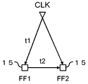
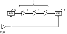
- the semiconductor integrated circuit includes a logic element 1 (FIG. 11) for performing operations and operation control, and a sequential circuit element 5 (also called a flip-flop) for synchronizing the operations of the logic element group 3 (FF1 in FIG. 11). , FF2).
- Each flip-flop 5 is supplied with a clock signal CLK that periodically oscillates, and the data held by the flip-flop 5 is supplied to the logic element 1 in response to the rise or fall of the clock signal CLK. Performs the operation and control of the operation using the supplied data as an input, and stores the result in the flip-flop 5. The above processing is repeated according to the rising or falling edge of the clock signal CLK that periodically changes.
- a delay analysis of the clock signal CLK supplied to the flip-flop 5 is performed, and it is verified by simulating whether the circuit operates at a normal timing based on the clock signal CLK.
- Patent Document 1 An example of a timing verification method for verifying operation timing in consideration of a voltage drop of a power supply wiring in a semiconductor integrated circuit is described in Patent Document 1.
- the maximum power supply voltage drop allowed in a semiconductor chip is set as a target power supply voltage drop, and the power supply voltage drop for timing verification is set based on the target power supply voltage drop.
- the power supply voltage drop amount for each cell obtained from the analysis result of the power supply network analysis is calculated for the timing verification.
- the second timing verification is performed by reviewing the delay variation according to the power supply voltage drop amount for cells having different values.
- Patent Document 2 describes an example of a semiconductor design support apparatus that performs logic simulation analysis / STA analysis in consideration of noise.
- the semiconductor design support apparatus of Patent Document 2 includes a power supply noise amount library and an output signal change amount library in the semiconductor design support apparatus.
- the power supply noise amount library analyzes power supply noise generated in an input / output unit.
- the obtained power supply noise data is stored.
- the output signal change amount library stores output signal change data indicating a signal waveform that changes in response to power supply noise data.
- the semiconductor design support apparatus described in Patent Document 2 generates a noise-compatible I / O layout model indicating an input / output unit of a semiconductor device corresponding to power supply noise, and outputs signal change data and a noise-compatible I / O layout model. Based on the above, the operation timing of the semiconductor device is predicted.
- Patent document 3 can verify power supply voltage drop and ground bounce, which are problems in large-scale CMOS LSIs, at the design stage before chip manufacture, and can provide an index for optimizing power supply wiring.
- a logic circuit operation verification device capable of detecting a propagation delay margin caused by a power supply voltage drop or ground bounce is described.
- Patent Document 4 describes a semiconductor integrated circuit simulation apparatus and simulation method that can obtain a delay simulation result with high accuracy by reflecting time-series voltage fluctuation information in a delay simulation.
- Patent Document 5 discloses a delay calculation apparatus and method for a semiconductor integrated circuit that performs highly reliable delay calculation and timing verification by calculating a voltage drop due to power supply wiring and considering the voltage drop for each element type. A timing verification apparatus and method are described.
- Patent Documents 6 to 12 describe examples of timing verification methods for verifying operation timing in consideration of a voltage drop of a power supply wiring in a semiconductor integrated circuit.
- the present invention has been made in view of the above circumstances, and an object of the present invention is a semiconductor capable of performing delay analysis in consideration of the influence when the voltage fluctuates due to noise applied from the outside of the chip.
- An object of the present invention is to provide an integrated circuit design apparatus, a data processing method thereof, and a control program thereof.
- a semiconductor integrated circuit design apparatus comprises: delay analysis means for performing static delay analysis of each path between flip-flops of the semiconductor integrated circuit based on chip information of the semiconductor integrated circuit; Noise generating means for generating noise information of noise applied to the semiconductor integrated circuit based on a predetermined noise definition; Voltage fluctuation amount analyzing means for analyzing a voltage fluctuation amount of the semiconductor integrated circuit when the noise is applied to a predetermined location of the semiconductor integrated circuit based on the noise information based on the chip information of the semiconductor integrated circuit; , Based on the voltage fluctuation amount analyzed by the voltage fluctuation amount analysis means, the delay analysis means performs the static delay analysis, and based on the result of the static delay analysis of each path of the semiconductor integrated circuit. Timing verification means for performing timing verification of the operation of the semiconductor integrated circuit, The noise generation means generates noise information of noise applied at a predetermined application timing, The timing verification means performs the timing verification for each noise applied at the predetermined application timing.
- the data processing method of the semiconductor integrated circuit design apparatus performs static delay analysis of each path between flip-flops of the semiconductor integrated circuit based on chip information of the semiconductor integrated circuit, Based on a predetermined noise definition, generating noise information of noise applied to the semiconductor integrated circuit at a predetermined application timing, Based on the chip information of the semiconductor integrated circuit, analyzing the voltage fluctuation amount of the semiconductor integrated circuit when applying the noise based on the noise information to a predetermined location of the semiconductor integrated circuit, In accordance with the analyzed voltage fluctuation amount, based on the chip information of the semiconductor integrated circuit, performing a static delay analysis of each path between the flip-flops of the semiconductor integrated circuit, For each of the noises applied at the predetermined application timing, the operation verification of the semiconductor integrated circuit is performed based on the result of the static delay analysis of each path of the semiconductor integrated circuit.
- a control program for a semiconductor integrated circuit design apparatus includes a procedure for performing a static delay analysis of each path between flip-flops of the semiconductor integrated circuit based on chip information of the semiconductor integrated circuit, Generating noise information of a predetermined noise to be applied to the semiconductor integrated circuit based on a predetermined noise definition; A step of analyzing a voltage fluctuation amount of the semiconductor integrated circuit when the noise is applied based on the noise information to a predetermined portion of the semiconductor integrated circuit based on the chip information of the semiconductor integrated circuit; Based on the voltage fluctuation amount analyzed by the procedure of analyzing the voltage fluctuation amount, a procedure for performing the static delay analysis in a procedure of performing the static delay analysis, A procedure for performing timing verification of the operation of the semiconductor integrated circuit based on the result of the static delay analysis of each path of the semiconductor integrated circuit; A procedure for generating noise information of noise applied at a predetermined application timing; A program for causing a computer to execute a procedure for performing the timing verification for each noise applied at the predetermined application timing.
- a plurality of components are formed as a single member, and a single component is formed of a plurality of members. It may be that a certain component is a part of another component, a part of a certain component overlaps with a part of another component, or the like.
- the data processing method and the computer program of the present invention describe a plurality of procedures in order, the described order does not limit the order in which the plurality of procedures are executed. For this reason, when implementing the data processing method and computer program of this invention, the order of the several procedure can be changed in the range which does not interfere in content.
- the data processing method and the plurality of procedures of the computer program of the present invention are not limited to being executed at different timings. For this reason, another procedure may occur during the execution of a certain procedure, or some or all of the execution timing of a certain procedure and the execution timing of another procedure may overlap.
- the present invention when a voltage fluctuates due to noise applied from the outside of a chip, it is possible to perform delay analysis in consideration of the influence, a data processing method thereof, and a control program thereof Is provided.
- FIG. 4 is a flowchart showing an example of the operation of the semiconductor integrated circuit design apparatus according to the embodiment of the present invention. It is a functional block diagram which shows the structure of the semiconductor integrated circuit design apparatus which concerns on embodiment of this invention. It is a figure for demonstrating the path delay time in the semiconductor integrated circuit design apparatus which concerns on embodiment of this invention. It is a figure for demonstrating an example when the noise number of the noise produced
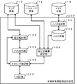
- FIG. 1 is a functional block diagram showing a configuration of a semiconductor integrated circuit design apparatus 100 according to an embodiment of the present invention.
- the semiconductor integrated circuit design device 100 of the present embodiment includes a delay analysis unit 102 that performs static delay analysis of each path between flip-flops included in the semiconductor integrated circuit based on chip information of the semiconductor integrated circuit (not shown), A noise generator 104 that generates noise information of noise applied to the semiconductor integrated circuit based on a predetermined noise definition, and noise based on the noise information at a predetermined location of the semiconductor integrated circuit based on chip information of the semiconductor integrated circuit.
- the delay analysis unit 102 Based on the voltage fluctuation amount analysis unit 106 that analyzes the voltage fluctuation amount of the semiconductor integrated circuit when applied, and the voltage fluctuation amount analyzed by the voltage fluctuation amount analysis unit 106, the delay analysis unit 102 performs static delay analysis. And a timing verification unit 108 for verifying the timing of the operation of the semiconductor integrated circuit based on the result of the static delay analysis of each path of the semiconductor integrated circuit. It includes a noise generating unit 104 generates a noise information of the noise to be applied at a predetermined application timing, timing verification unit 108 performs timing verification for each noise applied at a predetermined application timing.
- the semiconductor integrated circuit design device 100 of this embodiment can be configured by a general computer including a control device, a storage device, an input device, and a display device. These parts are not shown. Each unit is constructed and controlled on a storage device such as a ROM (Read Only Memory) or a RAM (Random Access Memory) by a control device that operates according to a computer program stored in the storage device.
- a storage device such as a ROM (Read Only Memory) or a RAM (Random Access Memory)
- each component of the semiconductor integrated circuit design apparatus 100 includes a CPU (Central Processing Unit) of an arbitrary computer, a memory, a program that realizes the components of the drawing loaded in the memory, and a hard disk that stores the program. It is realized by any combination of hardware and software, centering on the storage unit and network connection interface. It will be understood by those skilled in the art that there are various modifications to the implementation method and apparatus. Each drawing described below shows a functional unit block, not a hardware unit configuration.
- the semiconductor integrated circuit design device 100 can be included in, for example, a CAD (Computer Aided Design) system.
- CAD Computer Aided Design
- the semiconductor integrated circuit design device 100 of this embodiment includes a delay analysis unit 102, a noise generation unit 104, a voltage variation analysis unit 106, and a timing verification unit 108.
- the semiconductor integrated circuit design device 100 includes a chip information storage unit (shown as “chip information” in the figure) 10, a package information storage unit (shown as “package information” in the figure) 12, and a noise definition storage unit (shown in the figure). 14) (shown as “noise definition”).
- the semiconductor integrated circuit design device 100 reads the chip information, package information, and noise definition information of the semiconductor integrated circuit stored in the chip information storage unit 10, the package information storage unit 12, and the noise definition storage unit 14, respectively. it can.
- Each storage unit may be included in the semiconductor integrated circuit design device 100, may be included in a server device connected to the semiconductor integrated circuit design device 100 via a network, or may be included in the semiconductor integrated circuit design device 100. It may be included in an external storage device to be connected, or may be included in various recording media accessible by a recording medium reader connected to the semiconductor integrated circuit design device 100.
- the chip information stored in the chip information storage unit 10 includes, for example, a semiconductor integrated circuit netlist, layout information, a cell delay library, and a technology library.
- the noise definition information stored in the noise definition storage unit 14 is information defining noise applied to the semiconductor integrated circuit.
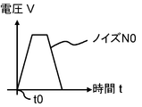
- the noise N0 defined by the noise definition information is represented by the relationship between the time t and the voltage V, with the time t0 being the noise application start time.
- the noise N0 is a trapezoidal wave as a typical example, but is not limited thereto, and may be any noise waveform.
- the delay analysis unit 102 is a delay analysis device generally used when designing a semiconductor integrated circuit.
- the delay analysis unit 102 inputs chip information data of the semiconductor integrated circuit from the chip information storage unit 10, analyzes the static delay, and outputs a report thereof.
- the delay analysis unit 102 performs RC extraction from layout information and a technology library, and performs static delay analysis using the extracted RC information, a net list, and a cell delay library.
- As a result of the delay analysis performed by the delay analysis unit 102 when a path that does not satisfy the design constraint condition is found, it is possible to design a circuit that satisfies the design constraint condition by performing relocation and wiring of the cell. Become. Note that the delay analysis and the report output of the analysis result are understood by those skilled in the art and are not related to the essence of the present invention, and thus detailed description thereof is omitted.
- the noise generation unit 104 generates noise information of noise applied to the semiconductor integrated circuit based on predetermined noise definition information (FIG. 2) stored in the noise definition storage unit 14, and the voltage fluctuation amount analysis unit 106 described later. input.
- the noise generation unit 104 can generate noise information that causes the noise defined by the noise definition to be applied to the semiconductor integrated circuit at various timings within the clock cycle.
- the voltage variation analysis unit 106 receives chip information from the chip information storage unit 10, package information from the package information storage unit 12, and noise information from the noise generation unit 104 as inputs, and receives a predetermined portion of the package, for example, a power supply voltage unit ( The voltage (VVDD and VGND) waveforms appearing at the VDD terminal and the GND terminal of each cell in the chip when noise is applied are obtained.
- a power supply voltage unit The voltage (VVDD and VGND) waveforms appearing at the VDD terminal and the GND terminal of each cell in the chip when noise is applied are obtained.
- the package is a circuit that connects the substrate and the chip, but the package handled here is a power supply circuit modeled by RLC.
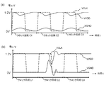
- the voltage waveform obtained by the voltage variation analysis unit 106 includes normal voltage variation during circuit operation and voltage variation due to noise applied to the package.
- the timing verification unit 108 is performed by a circuit simulator generally used when designing a semiconductor integrated circuit. The delay analysis of the path between each cell of the semiconductor integrated circuit is performed. At this time, the voltage data output from the voltage variation analysis unit 106 is used for the voltages (VVDD and VGND) at the VDD terminal and the GND terminal of each cell. That is, in this embodiment, the timing verification unit 108 can perform path delay analysis in consideration of the influence of noise applied from the outside by using the voltage data output from the voltage fluctuation amount analysis unit 106. it can.
- the CPU can realize each function of each unit by reading a program stored in the hard disk into the memory and executing it.
- the computer program according to the present embodiment performs static delay analysis of each path between flip-flops included in a semiconductor integrated circuit on the basis of chip information of the semiconductor integrated circuit in a computer for realizing the semiconductor integrated circuit design apparatus 100.
- a procedure for generating noise information of a predetermined noise to be applied to the semiconductor integrated circuit based on a predetermined noise definition, and a chip location of the semiconductor integrated circuit based on the noise information at a predetermined location of the semiconductor integrated circuit Static delay analysis is performed in the procedure for performing static delay analysis based on the procedure for analyzing the voltage fluctuation amount of the semiconductor integrated circuit when noise is applied and the voltage fluctuation amount analyzed by the procedure for analyzing the voltage fluctuation amount.
- the control program of the semiconductor integrated circuit design apparatus may be recorded on a computer-readable recording medium.
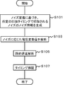
- FIG. 3 is a flowchart showing an example of the operation of the semiconductor integrated circuit design apparatus 100 of this embodiment.
- the data processing method of the semiconductor integrated circuit design apparatus 100 performs static delay analysis of each path between flip-flops included in the semiconductor integrated circuit based on chip information of the semiconductor integrated circuit, and defines a predetermined noise definition. Based on the noise information, a noise information of noise applied to the semiconductor integrated circuit at a predetermined application timing is generated (step S101). Based on the chip information of the semiconductor integrated circuit, a predetermined location of the semiconductor integrated circuit is generated. The voltage fluctuation amount of the semiconductor integrated circuit when noise is applied is analyzed (step S103), and each flip-flop between the flip-flops included in the semiconductor integrated circuit is analyzed based on the chip information of the semiconductor integrated circuit according to the analyzed voltage fluctuation amount. Path static delay analysis is performed (step S105), and semiconductor integration is performed for each noise applied at a predetermined application timing. Based on the results of the static timing analysis of each path of the road, performing timing verification of an operation of the semiconductor integrated circuit (step S107).
- the noise generation unit 104 generates noise information of noise applied at a certain application timing based on a predetermined noise definition (step S101).
- the voltage fluctuation amount analysis unit 106 analyzes voltage fluctuations when noise applied to the semiconductor integrated circuit at a certain timing generated by the noise generation unit 104 is applied to a certain part of the semiconductor integrated circuit (step S103).
- the voltage variation analysis unit 106 receives chip information from the chip information storage unit 10, package information from the package information storage unit 12, and noise information from the noise generation unit 104 as inputs.
- the voltage variation analyzing unit 106 applies a voltage (VVDD) appearing at the VDD terminal and the GND terminal of each cell in the chip when noise is applied to a predetermined portion of the package, for example, a power supply voltage unit (not shown).
- VGND voltage waveform
- the voltage fluctuation is also called voltage drop or IR (Interconnection Resistance) -drop.
- the timing verification unit 108 inputs the voltage output from the voltage variation analysis unit 106 to the VDD terminal and the GND terminal of each cell, and causes the delay analysis unit 102 to analyze the delay of the path between the cells. (Step S105), the operation timing of the semiconductor integrated circuit is verified (Step S107).
- the semiconductor integrated circuit design apparatus 100 of the embodiment of the present invention it is possible to perform a delay analysis in consideration of the influence of externally applied noise.
- the reason is that the normal voltage fluctuation amount due to the operation of the chip is almost the same every clock cycle, but it is not known when the power supply noise applied from the outside of the chip occurs.
- by applying noise to the outside of the chip at an arbitrary timing it can be determined when the circuit can operate correctly when noise is applied from the outside of the chip.
- the semiconductor integrated circuit design device 200 of this embodiment performs delay analysis in consideration of voltage fluctuations when a plurality of noises are shifted in the clock cycle and applied to the semiconductor integrated circuit, unlike the above embodiments. It is different in point.
- FIG. 4 is a functional block diagram showing the configuration of the semiconductor integrated circuit design apparatus 200 of this embodiment.
- the semiconductor integrated circuit design device 200 of this embodiment includes the same delay analysis unit 102, noise generation unit 104, and voltage fluctuation amount analysis unit 106 as the semiconductor integrated circuit design device 100 of the above embodiment of FIG.
- a unit 202 (shown as “noise information” in the figure), a path extraction unit 204, a determination unit 206, and a timing verification unit 208 are further provided.
- the noise information storage unit 202 stores the noise information generated by the noise generation unit 104.
- the noise generation unit 104 generates noise information that simulates a plurality of noises that are applied at different intervals within a clock cycle, and stores the noise information in the noise information storage unit 202. That is, the noise generation unit 104 can generate noise information so as to simulate noise that is irregularly applied from the outside of the semiconductor integrated circuit.
- the voltage fluctuation amount analysis unit 106 can sequentially read noise information of a plurality of noises stored in the noise information storage unit 202 and simulate the noise applied at different intervals within the clock cycle.
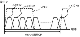
- the noise cycle Nn is repeatedly applied n times while equally dividing the clock cycle CP into n (n is a natural number) and shifting the interval at n different timings. Can be simulated.
- the voltage fluctuation amount analysis unit 106 starts from the noise N1 in FIG. . .
- the analysis is repeated n times in order for the noise Nn. Thereby, the influence of the noise applied at n different timings can be considered. In this way, the generated n noises can simulate noise generated at a timing unrelated to the variation of the clock voltage VCLK that varies in accordance with the clock cycle CP.
- the timing verification unit 208 causes the delay analysis unit 102 to execute the delay analysis by shifting the interval of the noise application timing within the clock cycle CP. Repeat timing verification. That is, the noise generation unit 104 generates noise information of n pieces of noise N1 to Nn and stores the noise information in the noise information storage unit 202.
- the voltage variation analysis unit 106 refers to the noise information storage unit 202, and each noise is stored. For Ni (i is an integer from 1 to n), the voltage fluctuation amount analysis is sequentially performed.
- the delay analysis unit 102 performs a delay analysis based on the voltage fluctuation amount analyzed in consideration of the influence of the noise Ni. As described above, based on the analysis result in consideration of the influence of the noise Ni, the timing verification unit 208 repeatedly performs the timing verification for each noise Ni n times.
Landscapes
- Engineering & Computer Science (AREA)
- Computer Hardware Design (AREA)
- Physics & Mathematics (AREA)
- Theoretical Computer Science (AREA)
- Evolutionary Computation (AREA)
- Geometry (AREA)
- General Engineering & Computer Science (AREA)
- General Physics & Mathematics (AREA)
- Design And Manufacture Of Integrated Circuits (AREA)
Abstract
Description
この他にも、半導体集積回路における電源配線の電圧降下を考慮して動作タイミングの検証を行うタイミング検証方法の例が特許文献6乃至12に記載されている。
所定のノイズ定義に基づいて前記半導体集積回路に印加するノイズのノイズ情報を生成するノイズ生成手段と、
前記半導体集積回路の前記チップ情報に基づいて、前記半導体集積回路の所定箇所に前記ノイズ情報に基づいて前記ノイズを印加した時の前記半導体集積回路の電圧変動量を解析する電圧変動量解析手段と、
前記電圧変動量解析手段により解析された前記電圧変動量に基づいて、前記遅延解析手段に前記静的遅延解析を行わせ、前記半導体集積回路の前記各パスの前記静的遅延解析の結果に基づいて、前記半導体集積回路の動作のタイミング検証を行うタイミング検証手段と、を備え、
前記ノイズ生成手段は、所定の印加タイミングで印加されるノイズのノイズ情報を生成し、
前記タイミング検証手段は、前記所定の印加タイミングで印加される前記ノイズ毎に前記タイミング検証を行う。
所定のノイズ定義に基づいて、前記半導体集積回路に所定の印加タイミングで印加されるノイズのノイズ情報を生成し、
前記半導体集積回路の前記チップ情報に基づいて、前記半導体集積回路の所定箇所に、前記ノイズ情報に基づいて前記ノイズを印加した時の前記半導体集積回路の電圧変動量を解析し、
解析された前記電圧変動量に応じ、前記半導体集積回路の前記チップ情報に基づいて、前記半導体集積回路が有するフリップフロップ間の各パスの静的遅延解析を行い、
前記所定の印加タイミングで印加される前記ノイズ毎に、前記半導体集積回路の前記各パスの前記静的遅延解析の結果に基づいて、前記半導体集積回路の動作のタイミング検証を行う。
所定のノイズ定義に基づいて前記半導体集積回路に印加する所定のノイズのノイズ情報を生成する手順と、
前記半導体集積回路の前記チップ情報に基づいて、前記半導体集積回路の所定箇所に前記ノイズ情報に基づいて前記ノイズを印加した時の前記半導体集積回路の電圧変動量を解析する手順と、
前記電圧変動量を解析する手順により解析された前記電圧変動量に基づいて、前記静的遅延解析を行う手順に前記静的遅延解析を行わせる手順と、
前記半導体集積回路の前記各パスの前記静的遅延解析の結果に基づいて、前記半導体集積回路の動作のタイミング検証を行う手順と、
所定の印加タイミングで印加されるノイズのノイズ情報を生成する手順と、
前記所定の印加タイミングで印加される前記ノイズ毎に前記タイミング検証を行う手順と、をコンピュータに実行させるためのプログラム。
図1は、本発明の実施形態に係る半導体集積回路設計装置100の構成を示す機能ブロック図である。
本実施形態の半導体集積回路設計装置100は、半導体集積回路(不図示)のチップ情報に基づいて、半導体集積回路が有するフリップフロップ間の各パスの静的遅延解析を行う遅延解析部102と、所定のノイズ定義に基づいて半導体集積回路に印加するノイズのノイズ情報を生成するノイズ生成部104と、半導体集積回路のチップ情報に基づいて、半導体集積回路の所定箇所にノイズ情報に基づいてノイズを印加した時の半導体集積回路の電圧変動量を解析する電圧変動量解析部106と、電圧変動量解析部106により解析された電圧変動量に基づいて、遅延解析部102に静的遅延解析を行わせ、半導体集積回路の各パスの静的遅延解析の結果に基づいて、半導体集積回路の動作のタイミング検証を行うタイミング検証部108と、を備え、ノイズ生成部104は、所定の印加タイミングで印加されるノイズのノイズ情報を生成し、タイミング検証部108は、所定の印加タイミングで印加されるノイズ毎にタイミング検証を行う。
図3は、本実施形態の半導体集積回路設計装置100の動作の一例を示すフローチャートである。
本実施形態の半導体集積回路設計装置200は、上記実施の形態とは、複数のノイズをクロック周期内で間隔をずらして、半導体集積回路に印加した場合の電圧変動を考慮して遅延解析を行う点で相違する。
図7は、本実施形態の半導体集積回路設計装置200の動作の一例を示すフローチャートである。本実施形態の半導体集積回路設計装置200は、上記実施形態の半導体集積回路設計装置100と同じステップS105およびステップS107を有し、さらに、ステップS201~ステップS213を有する。
本実施形態の半導体集積回路設計装置300は、上記実施の形態とは、解析に使用するノイズ数を絞る点で相違する。本実施形態の半導体集積回路設計装置300は、半導体集積回路の各パスの静的遅延解析の結果に基づいて、タイミング検証部208がタイミング検証を繰り返す回数を削減する制御部302をさらに備える。
あるチップについてノイズ影響を考慮した遅延解析を実施した。静的遅延解析を行う遅延解析部として、Cadence社製Encounter(登録商標)を用い、電圧変動量解析を行う電圧変動量解析部としてApache社製RedHawk(商標)を用い、タイミング検証を行うタイミング検証部としてSPICE(商標)を使用した。
Claims (17)
- 半導体集積回路のチップ情報に基づいて、前記半導体集積回路が有するフリップフロップ間の各パスの静的遅延解析を行う遅延解析手段と、
所定のノイズ定義に基づいて前記半導体集積回路に印加するノイズのノイズ情報を生成するノイズ生成手段と、
前記半導体集積回路の前記チップ情報に基づいて、前記半導体集積回路の所定箇所に前記ノイズ情報に基づいて前記ノイズを印加した時の前記半導体集積回路の電圧変動量を解析する電圧変動量解析手段と、
前記電圧変動量解析手段により解析された前記電圧変動量に基づいて、前記遅延解析手段に前記静的遅延解析を行わせ、前記半導体集積回路の前記各パスの前記静的遅延解析の結果に基づいて、前記半導体集積回路の動作のタイミング検証を行うタイミング検証手段と、を備え、
前記ノイズ生成手段は、所定の印加タイミングで印加されるノイズのノイズ情報を生成し、
前記タイミング検証手段は、前記所定の印加タイミングで印加される前記ノイズ毎に前記タイミング検証を行う半導体集積回路の設計装置。 - 請求項1に記載の半導体集積回路の設計装置において、
前記タイミング検証手段は、
前記ノイズの前記印加タイミングの間隔を、クロック周期内でずらして、前記半導体集積回路の前記タイミング検証を繰り返し実行する半導体集積回路の設計装置。 - 請求項2に記載の半導体集積回路の設計装置において、
前記半導体集積回路の前記各パスの前記静的遅延解析の結果に基づいて、前記タイミング検証手段が前記タイミング検証を繰り返す回数を削減する制御手段をさらに備える半導体集積回路の設計装置。 - 請求項3に記載の半導体集積回路の設計装置において、
前記制御手段は、
前記各パスの前記静的遅延解析の結果に基づいて、クロックソースから前記各パスの一方のフリップフロップに信号が伝達される第1遅延時間と、他方のフリップフロップに伝達される第2遅延時間との合計時間を算出し、前記クロック周期の始まりから前記合計時間内で、前記タイミング検証手段が前記タイミング検証を繰り返すように前記回数を削減する半導体集積回路の設計装置。 - 請求項1乃至4いずれかに記載の半導体集積回路の設計装置において、
前記タイミング検証手段の検証結果に基づいて、前記半導体集積回路の設計制約条件を満たしているか否かを判定する判定手段を備える半導体集積回路の設計装置。 - 請求項1乃至5いずれかに記載の半導体集積回路の設計装置において、
前記ノイズ定義を変更して、前記半導体集積回路の前記タイミング検証を繰り返し実行する半導体集積回路の設計装置。 - 請求項1乃至6いずれかに記載の半導体集積回路の設計装置において、
前記ノイズ生成手段が生成した前記ノイズ情報を記憶するノイズ情報記憶手段を備える半導体集積回路の設計装置。 - 請求項1乃至7いずれかに記載の半導体集積回路の設計装置において、
前記ノイズ生成手段は、前記ノイズ情報を、前記半導体集積回路の外部より不定期に印加されるノイズを模擬するように生成する半導体集積回路の設計装置。 - 半導体集積回路のチップ情報に基づいて、前記半導体集積回路が有するフリップフロップ間の各パスの静的遅延解析を行い、
所定のノイズ定義に基づいて、前記半導体集積回路に所定の印加タイミングで印加されるノイズのノイズ情報を生成し、
前記半導体集積回路の前記チップ情報に基づいて、前記半導体集積回路の所定箇所に、前記ノイズ情報に基づいて前記ノイズを印加した時の前記半導体集積回路の電圧変動量を解析し、
解析された前記電圧変動量に応じ、前記半導体集積回路の前記チップ情報に基づいて、前記半導体集積回路が有するフリップフロップ間の各パスの静的遅延解析を行い、
前記所定の印加タイミングで印加される前記ノイズ毎に、前記半導体集積回路の前記各パスの前記静的遅延解析の結果に基づいて、前記半導体集積回路の動作のタイミング検証を行う半導体集積回路の設計装置のデータ処理方法。 - 請求項9に記載の半導体集積回路の設計装置のデータ処理方法において、
前記ノイズの前記印加タイミングの間隔を、クロック周期内でずらして、前記半導体集積回路の前記タイミング検証を繰り返し実行する半導体集積回路の設計装置のデータ処理方法。 - 請求項10に記載の半導体集積回路の設計装置のデータ処理方法において、
前記半導体集積回路の前記各パスの前記静的遅延解析の結果に基づいて、前記タイミング検証を繰り返す回数を削減する半導体集積回路の設計装置のデータ処理方法。 - 請求項9乃至11いずれかに記載の半導体集積回路の設計装置のデータ処理方法において、
前記ノイズ情報を、前記半導体集積回路の外部より不定期に印加されるノイズを模擬するように生成する半導体集積回路の設計装置のデータ処理方法。 - 半導体集積回路のチップ情報に基づいて、前記半導体集積回路が有するフリップフロップ間の各パスの静的遅延解析を行う手順と、
所定のノイズ定義に基づいて前記半導体集積回路に印加する所定のノイズのノイズ情報を生成する手順と、
前記半導体集積回路の前記チップ情報に基づいて、前記半導体集積回路の所定箇所に前記ノイズ情報に基づいて前記ノイズを印加した時の前記半導体集積回路の電圧変動量を解析する手順と、
前記電圧変動量を解析する手順により解析された前記電圧変動量に基づいて、前記静的遅延解析を行う手順に前記静的遅延解析を行わせる手順と、
前記半導体集積回路の前記各パスの前記静的遅延解析の結果に基づいて、前記半導体集積回路の動作のタイミング検証を行う手順と、
所定の印加タイミングで印加されるノイズのノイズ情報を生成する手順と、
前記所定の印加タイミングで印加される前記ノイズ毎に前記タイミング検証を行う手順と、をコンピュータに実行させるための半導体集積回路の設計装置の制御プログラム。 - 請求項13に記載の半導体集積回路の設計装置の制御プログラムにおいて、
前記ノイズ情報を生成する手順による前記ノイズの前記印加タイミングの間隔を、クロック周期内でずらして、前記半導体集積回路の前記タイミング検証を繰り返し実行する手順をさらにコンピュータに実行させるための半導体集積回路の設計装置の制御プログラム。 - 請求項14に記載の半導体集積回路の設計装置の制御プログラムにおいて、
前記半導体集積回路の前記各パスの前記静的遅延解析の結果に基づいて、前記タイミング検証を繰り返す回数を削減する手順をコンピュータに実行させるための半導体集積回路の設計装置の制御プログラム。 - 請求項13乃至15いずれかに記載の半導体集積回路の設計装置の制御プログラムにおいて、
前記ノイズ情報を、前記半導体集積回路の外部より不定期に印加されるノイズを模擬するように生成する手順をコンピュータに実行させるための半導体集積回路の設計装置の制御プログラム。 - 請求項13乃至16いずれかに記載の半導体集積回路の設計装置の制御プログラムを記録したコンピュータで読み取り可能な記録媒体。
Priority Applications (2)
| Application Number | Priority Date | Filing Date | Title |
|---|---|---|---|
| US13/262,759 US8458633B2 (en) | 2009-05-20 | 2010-04-21 | Semiconductor integrated circuit design apparatus and method for analyzing a delay in a semiconductor integrated circuit |
| JP2011514306A JP5119506B2 (ja) | 2009-05-20 | 2010-04-21 | 半導体集積回路の設計装置、そのデータ処理方法、およびその制御プログラム |
Applications Claiming Priority (2)
| Application Number | Priority Date | Filing Date | Title |
|---|---|---|---|
| JP2009121783 | 2009-05-20 | ||
| JP2009-121783 | 2009-05-20 |
Publications (1)
| Publication Number | Publication Date |
|---|---|
| WO2010134264A1 true WO2010134264A1 (ja) | 2010-11-25 |
Family
ID=43125957
Family Applications (1)
| Application Number | Title | Priority Date | Filing Date |
|---|---|---|---|
| PCT/JP2010/002881 Ceased WO2010134264A1 (ja) | 2009-05-20 | 2010-04-21 | 半導体集積回路の設計装置、そのデータ処理方法、およびその制御プログラム |
Country Status (3)
| Country | Link |
|---|---|
| US (1) | US8458633B2 (ja) |
| JP (1) | JP5119506B2 (ja) |
| WO (1) | WO2010134264A1 (ja) |
Cited By (2)
| Publication number | Priority date | Publication date | Assignee | Title |
|---|---|---|---|---|
| JP2019028907A (ja) * | 2017-08-03 | 2019-02-21 | 日本電信電話株式会社 | ノイズ波形モデル生成装置およびその生成方法 |
| CN109388826A (zh) * | 2017-08-09 | 2019-02-26 | 默升科技集团有限公司 | 使能2.5d器件级静态时序分析的管芯接口 |
Families Citing this family (3)
| Publication number | Priority date | Publication date | Assignee | Title |
|---|---|---|---|---|
| JP6017134B2 (ja) * | 2011-12-13 | 2016-10-26 | 東京エレクトロン株式会社 | 生産効率化システム、生産効率化装置および生産効率化方法 |
| US8707234B1 (en) * | 2012-11-09 | 2014-04-22 | Lsi Corporation | Circuit noise extraction using forced input noise waveform |
| US20230289507A1 (en) * | 2022-03-11 | 2023-09-14 | Nvidia Corporation | Analyzing integrated circuit timing variation |
Citations (2)
| Publication number | Priority date | Publication date | Assignee | Title |
|---|---|---|---|---|
| JP2002270695A (ja) * | 2001-03-08 | 2002-09-20 | Matsushita Electric Ind Co Ltd | 電磁波障害解析方法および電磁波障害解析装置およびこれを用いた半導体装置の製造方法 |
| JP2008287666A (ja) * | 2007-05-21 | 2008-11-27 | Sharp Corp | 回路動作検証装置、半導体集積回路の製造方法、回路動作検証方法、制御プログラムおよび可読記録媒体 |
Family Cites Families (17)
| Publication number | Priority date | Publication date | Assignee | Title |
|---|---|---|---|---|
| JP2708338B2 (ja) | 1992-10-12 | 1998-02-04 | 三菱電機株式会社 | 論理シミュレーション装置及び回路シミュレーション装置 |
| JPH07239865A (ja) | 1994-02-25 | 1995-09-12 | Matsushita Electric Ind Co Ltd | 論理シミュレータ |
| JPH0954798A (ja) | 1995-08-10 | 1997-02-25 | Nec Corp | 遅延シミュレーションシステム |
| JP2000148826A (ja) | 1998-11-12 | 2000-05-30 | Sony Corp | 論理回路動作検証装置 |
| JP2000194732A (ja) | 1998-12-24 | 2000-07-14 | Nec Ic Microcomput Syst Ltd | 半導体集積回路のシミュレーション装置およびシミュレーション方法 |
| JP2000195960A (ja) | 1998-12-25 | 2000-07-14 | Matsushita Electric Ind Co Ltd | 半導体集積回路の遅延計算装置及びその方法並びにタイミング検証装置及びその方法 |
| JP2003271696A (ja) | 2002-03-19 | 2003-09-26 | Fujitsu Ltd | 電圧変動反映遅延計算方法および電圧変動反映遅延計算システム |
| JP4095396B2 (ja) | 2002-09-30 | 2008-06-04 | 富士通株式会社 | タイミング検証方法、タイミング検証装置、プログラム、及び記録媒体 |
| JP2005004268A (ja) | 2003-06-09 | 2005-01-06 | Matsushita Electric Ind Co Ltd | 半導体集積回路装置の動作解析方法、これに用いられる解析装置およびこれを用いた最適化設計方法 |
| JP2006215987A (ja) | 2005-02-07 | 2006-08-17 | Sharp Corp | 電圧降下量計算方法及び電圧降下量計算装置、回路検証方法及び回路検証装置、並びに回路設計方法及び回路設計装置 |
| US7313771B2 (en) * | 2005-03-31 | 2007-12-25 | Fujitsu Limited | Computing current in a digital circuit based on an accurate current model for library cells |
| US20070136705A1 (en) * | 2005-12-09 | 2007-06-14 | Fujitsu Limited | Timing analysis method and device |
| US7490309B1 (en) * | 2006-08-31 | 2009-02-10 | Cadence Design Systems, Inc. | Method and system for automatically optimizing physical implementation of an electronic circuit responsive to simulation analysis |
| JP2008083815A (ja) | 2006-09-26 | 2008-04-10 | Nec Electronics Corp | 半導体設計支援装置 |
| JP4946573B2 (ja) | 2007-03-30 | 2012-06-06 | 富士通セミコンダクター株式会社 | デカップリングセル配置方法及びデカップリングセル配置装置 |
| JP4422179B2 (ja) * | 2007-10-19 | 2010-02-24 | 株式会社半導体理工学研究センター | 半導体集積回路のタイミング解析装置及び方法 |
| JP5217418B2 (ja) * | 2007-12-25 | 2013-06-19 | 富士通セミコンダクター株式会社 | 半導体装置、容量値算出方法 |
-
2010
- 2010-04-21 JP JP2011514306A patent/JP5119506B2/ja not_active Expired - Fee Related
- 2010-04-21 US US13/262,759 patent/US8458633B2/en not_active Expired - Fee Related
- 2010-04-21 WO PCT/JP2010/002881 patent/WO2010134264A1/ja not_active Ceased
Patent Citations (2)
| Publication number | Priority date | Publication date | Assignee | Title |
|---|---|---|---|---|
| JP2002270695A (ja) * | 2001-03-08 | 2002-09-20 | Matsushita Electric Ind Co Ltd | 電磁波障害解析方法および電磁波障害解析装置およびこれを用いた半導体装置の製造方法 |
| JP2008287666A (ja) * | 2007-05-21 | 2008-11-27 | Sharp Corp | 回路動作検証装置、半導体集積回路の製造方法、回路動作検証方法、制御プログラムおよび可読記録媒体 |
Cited By (3)
| Publication number | Priority date | Publication date | Assignee | Title |
|---|---|---|---|---|
| JP2019028907A (ja) * | 2017-08-03 | 2019-02-21 | 日本電信電話株式会社 | ノイズ波形モデル生成装置およびその生成方法 |
| CN109388826A (zh) * | 2017-08-09 | 2019-02-26 | 默升科技集团有限公司 | 使能2.5d器件级静态时序分析的管芯接口 |
| CN109388826B (zh) * | 2017-08-09 | 2023-09-12 | 默升科技集团有限公司 | 使能2.5d器件级静态时序分析的管芯接口 |
Also Published As
| Publication number | Publication date |
|---|---|
| JP5119506B2 (ja) | 2013-01-16 |
| US8458633B2 (en) | 2013-06-04 |
| JPWO2010134264A1 (ja) | 2012-11-08 |
| US20120096421A1 (en) | 2012-04-19 |
Similar Documents
| Publication | Publication Date | Title |
|---|---|---|
| US7356789B2 (en) | Metastability effects simulation for a circuit description | |
| US7243322B1 (en) | Metastability injector for a circuit description | |
| KR100517537B1 (ko) | 반도체 집적회로의 설계방법 | |
| US9767239B1 (en) | Timing optimization driven by statistical sensitivites | |
| JP5119506B2 (ja) | 半導体集積回路の設計装置、そのデータ処理方法、およびその制御プログラム | |
| CN115618779B (zh) | 一种考虑标准单元老化效应的仿真分析方法 | |
| JP5040758B2 (ja) | シミュレーション装置、シミュレーション方法及びプログラム | |
| US8255859B2 (en) | Method and system for verification of multi-voltage circuit design | |
| JP2005339060A (ja) | クロストーク計算装置およびクロストーク計算方法 | |
| CN113536726A (zh) | 用于最大瞬时峰值功率的矢量生成 | |
| JP4554509B2 (ja) | タイミング解析装置及びタイミング解析手法 | |
| US20110307234A1 (en) | Circuit simulation method and circuit simulation device | |
| JP4066399B2 (ja) | 集積回路におけるホットキャリア効果のシミュレーション方法 | |
| JP2008083815A (ja) | 半導体設計支援装置 | |
| JP2007233454A (ja) | ノイズライブラリの作成方法、ノイズライブラリの作成プログラム、およびノイズライブラリの作成装置 | |
| JPWO2010101029A1 (ja) | 半導体集積回路設計装置、半導体集積回路設計方法、及び半導体集積回路設計プログラム | |
| JP2009187119A (ja) | 検証支援プログラム、検証支援装置、および検証支援方法 | |
| JP2005259107A (ja) | 回路シミュレーション方法および回路シミュレーション装置 | |
| US9460249B2 (en) | Verification of asynchronous clocking systems | |
| Gibson Jr | Modeling Single Event Transient Filters Through Gate-Level Simulations With Timing | |
| KR20060086222A (ko) | 이벤트 구동 스위치 레벨 시뮬레이션 방법 및 시뮬레이터 | |
| JP2007086939A (ja) | 回路シミュレーション方法 | |
| JP2008152329A (ja) | 回路解析方法、及び回路解析プログラム、回路シミュレーション装置 | |
| JP2012022566A (ja) | 半導体集積回路の設計装置および設計方法 | |
| JP2009187325A (ja) | 半導体集積回路の設計方法および設計支援装置 |
Legal Events
| Date | Code | Title | Description |
|---|---|---|---|
| 121 | Ep: the epo has been informed by wipo that ep was designated in this application |
Ref document number: 10777504 Country of ref document: EP Kind code of ref document: A1 |
|
| WWE | Wipo information: entry into national phase |
Ref document number: 2011514306 Country of ref document: JP |
|
| NENP | Non-entry into the national phase |
Ref country code: DE |
|
| WWE | Wipo information: entry into national phase |
Ref document number: 13262759 Country of ref document: US |
|
| 122 | Ep: pct application non-entry in european phase |
Ref document number: 10777504 Country of ref document: EP Kind code of ref document: A1 |