WO2010119639A1 - バックライト装置 - Google Patents
バックライト装置 Download PDFInfo
- Publication number
- WO2010119639A1 WO2010119639A1 PCT/JP2010/002485 JP2010002485W WO2010119639A1 WO 2010119639 A1 WO2010119639 A1 WO 2010119639A1 JP 2010002485 W JP2010002485 W JP 2010002485W WO 2010119639 A1 WO2010119639 A1 WO 2010119639A1
- Authority
- WO
- WIPO (PCT)
- Prior art keywords
- guide plate
- light guide
- light
- led
- interval
- Prior art date
Links
Images


Classifications
-
- G—PHYSICS
- G02—OPTICS
- G02B—OPTICAL ELEMENTS, SYSTEMS OR APPARATUS
- G02B6/00—Light guides; Structural details of arrangements comprising light guides and other optical elements, e.g. couplings
- G02B6/0001—Light guides; Structural details of arrangements comprising light guides and other optical elements, e.g. couplings specially adapted for lighting devices or systems
- G02B6/0011—Light guides; Structural details of arrangements comprising light guides and other optical elements, e.g. couplings specially adapted for lighting devices or systems the light guides being planar or of plate-like form
- G02B6/0033—Means for improving the coupling-out of light from the light guide
- G02B6/0035—Means for improving the coupling-out of light from the light guide provided on the surface of the light guide or in the bulk of it
- G02B6/0038—Linear indentations or grooves, e.g. arc-shaped grooves or meandering grooves, extending over the full length or width of the light guide
-
- G—PHYSICS
- G02—OPTICS
- G02B—OPTICAL ELEMENTS, SYSTEMS OR APPARATUS
- G02B6/00—Light guides; Structural details of arrangements comprising light guides and other optical elements, e.g. couplings
- G02B6/0001—Light guides; Structural details of arrangements comprising light guides and other optical elements, e.g. couplings specially adapted for lighting devices or systems
- G02B6/0011—Light guides; Structural details of arrangements comprising light guides and other optical elements, e.g. couplings specially adapted for lighting devices or systems the light guides being planar or of plate-like form
- G02B6/0013—Means for improving the coupling-in of light from the light source into the light guide
- G02B6/0023—Means for improving the coupling-in of light from the light source into the light guide provided by one optical element, or plurality thereof, placed between the light guide and the light source, or around the light source
- G02B6/0031—Reflecting element, sheet or layer
-
- G—PHYSICS
- G02—OPTICS
- G02B—OPTICAL ELEMENTS, SYSTEMS OR APPARATUS
- G02B6/00—Light guides; Structural details of arrangements comprising light guides and other optical elements, e.g. couplings
- G02B6/0001—Light guides; Structural details of arrangements comprising light guides and other optical elements, e.g. couplings specially adapted for lighting devices or systems
- G02B6/0011—Light guides; Structural details of arrangements comprising light guides and other optical elements, e.g. couplings specially adapted for lighting devices or systems the light guides being planar or of plate-like form
- G02B6/0066—Light guides; Structural details of arrangements comprising light guides and other optical elements, e.g. couplings specially adapted for lighting devices or systems the light guides being planar or of plate-like form characterised by the light source being coupled to the light guide
- G02B6/0068—Arrangements of plural sources, e.g. multi-colour light sources
-
- G—PHYSICS
- G02—OPTICS
- G02B—OPTICAL ELEMENTS, SYSTEMS OR APPARATUS
- G02B6/00—Light guides; Structural details of arrangements comprising light guides and other optical elements, e.g. couplings
- G02B6/0001—Light guides; Structural details of arrangements comprising light guides and other optical elements, e.g. couplings specially adapted for lighting devices or systems
- G02B6/0011—Light guides; Structural details of arrangements comprising light guides and other optical elements, e.g. couplings specially adapted for lighting devices or systems the light guides being planar or of plate-like form
- G02B6/0066—Light guides; Structural details of arrangements comprising light guides and other optical elements, e.g. couplings specially adapted for lighting devices or systems the light guides being planar or of plate-like form characterised by the light source being coupled to the light guide
- G02B6/0073—Light emitting diode [LED]
-
- G—PHYSICS
- G02—OPTICS
- G02B—OPTICAL ELEMENTS, SYSTEMS OR APPARATUS
- G02B6/00—Light guides; Structural details of arrangements comprising light guides and other optical elements, e.g. couplings
- G02B6/0001—Light guides; Structural details of arrangements comprising light guides and other optical elements, e.g. couplings specially adapted for lighting devices or systems
- G02B6/0011—Light guides; Structural details of arrangements comprising light guides and other optical elements, e.g. couplings specially adapted for lighting devices or systems the light guides being planar or of plate-like form
- G02B6/0081—Mechanical or electrical aspects of the light guide and light source in the lighting device peculiar to the adaptation to planar light guides, e.g. concerning packaging
- G02B6/0085—Means for removing heat created by the light source from the package
-
- G—PHYSICS
- G02—OPTICS
- G02B—OPTICAL ELEMENTS, SYSTEMS OR APPARATUS
- G02B6/00—Light guides; Structural details of arrangements comprising light guides and other optical elements, e.g. couplings
- G02B6/0001—Light guides; Structural details of arrangements comprising light guides and other optical elements, e.g. couplings specially adapted for lighting devices or systems
- G02B6/0011—Light guides; Structural details of arrangements comprising light guides and other optical elements, e.g. couplings specially adapted for lighting devices or systems the light guides being planar or of plate-like form
- G02B6/0081—Mechanical or electrical aspects of the light guide and light source in the lighting device peculiar to the adaptation to planar light guides, e.g. concerning packaging
- G02B6/0086—Positioning aspects
- G02B6/0091—Positioning aspects of the light source relative to the light guide
Definitions
- the present invention relates to a backlight device, and more particularly to a backlight device that emits light from the back surface of an image display panel.
- the LED is a point light source, it is necessary to arrange a plurality of LEDs along the end face of the light guide plate. At this time, it is necessary to appropriately suppress the luminous intensity unevenness caused by the arrangement interval. In addition, an increase in the size of the display is being promoted in parallel with the reduction in thickness, and it is necessary to increase the amount of light emitted from the entire backlight.
- many LEDs need to be arranged around the end face of the light guide plate.
- the LEDs arranged in parallel around one end surface of the light guide plate are not evenly spaced. Even in such a case, it is necessary to appropriately suppress the light intensity unevenness caused by the arrangement interval.
- the present invention has been made to solve the above-described problems, and its purpose is to suppress unevenness in luminous intensity caused by the arrangement interval of LEDs in a backlight device having a plurality of LEDs that emit light to the end face of the light guide plate. There is to do.
- a backlight device includes a light guide plate, and a plurality of white light emitting elements arranged in parallel in the extending direction of the end surface of the light guide plate with a distance H from the end surface of the light guide plate.
- the plurality of white light emitting diodes are arranged side by side so that the arrangement interval of the white light emitting diodes in a group constituted by two or more white light emitting diodes is P1 and the arrangement interval of the groups is P2, and the light guide plate is P1 ⁇ H It arrange
- positions so that ⁇ P2.
- the backlight device having a plurality of LEDs that emit light to the end face of the light guide plate, it is possible to suppress unevenness in light intensity caused by the arrangement interval of the LEDs.
- FIG. 1 is a cross-sectional view of an image display apparatus 10 according to the first embodiment.
- FIG. 1 shows a cross section of an upper portion of the image display device 10 when cut along a plane perpendicular to the horizontal direction of the device.
- the image display device 10 includes a liquid crystal panel 12, a front cover 13, a chassis 14, a cushion 16, an optical sheet 18, and a backlight device 20.
- the liquid crystal panel 12 is formed in a rectangular flat plate shape, and is arranged in front of the image display device 10 so that the display surface faces.
- a light shielding portion 12 a is provided at the edge of the liquid crystal panel 12.
- the chassis 14 has a cross section of a shape obtained by rotating the L shape by 180 degrees, and has a length in the left-right direction that is slightly longer than the liquid crystal panel 12.
- the chassis 14 is disposed above the liquid crystal panel 12 so as to cover the front of the apparatus and the upper part of the apparatus.
- a cushion 16 is provided at the lower part of the front surface of the chassis 14, and the light shielding part 12 a above the liquid crystal panel 12 is sandwiched between the cushion 16 and the front cover 13. Further, the rear surface of the chassis 14 is subjected to a white surface treatment so that the reflectance of light is increased.
- a backlight device 20 is provided on the rear side of the liquid crystal panel 12 and the chassis 14.
- the backlight device 20 includes a light guide plate 22, a rear plate 24, a heat sink 26, a heat radiation sheet 28, a substrate unit 30, and a reflection sheet 40.
- the heat sink 26, the heat dissipation sheet 28, and the board unit 30 are similarly provided in the lower part of the backlight device 20.
- the upper part of the backlight device 20 will be described, and the description of the heat sink 26, the heat dissipation sheet 28, and the board unit 30 provided below will be omitted.
- the arrangement positions of the heat sink 26, the heat radiating sheet 28, and the substrate unit 30 are not limited to the upper side and the lower side of the light guide plate 22. For example, these positions are on the right side and the left side of the light guide plate 22 when the image display device 10 is viewed from the front. May be arranged.
- the light guide plate 22 is formed to be slightly larger than the liquid crystal panel 12 by a transparent plate member.
- the light guide plate 22 is made of acrylic, and the thickness of the light guide plate 22 is 2 mm.
- the light guide plate 22 may be formed of other materials such as polycarbonate. Of course, the thickness of the light guide plate 22 is not limited to this value. In order to reduce the thickness of the entire image display device 10, the light guide plate 22 has a thickness of 1 mm to 5 mm. .
- the light guide plate 22 is disposed on the rear side of the liquid crystal panel 12 so as to cover the entire back surface side of the liquid crystal panel 12.
- a dot pattern 23 is formed on the surface of the light guide plate 22 opposite to the liquid crystal panel 12 and has a function of emitting light incident from the end surface 22a of the light guide plate 22 to the liquid crystal panel 12 side.
- the optical sheet 18 is formed by laminating a diffusion sheet, a prism sheet, and a polarization separation sheet. The optical sheet 18 is disposed between the liquid crystal panel 12 and the light guide plate 22.
- the rear plate 24 is formed of a sheet metal having a rectangular outer shape larger than the light guide plate 22.
- the rear plate 24 is disposed further to the rear side of the apparatus than the light guide plate 22.
- the reflection sheet 40 is formed in a rectangular shape larger than the light guide plate 22 and is disposed between the light guide plate 22 and the rear plate 24.
- the substrate unit 30 includes a flexible substrate 32 and an LED unit 34.
- the flexible substrate 32 is a substrate having general flexibility using a polyimide film as an insulator and a copper foil as a conductor, and has the same length as the entire length of the light guide plate 22 in the left-right direction of the device.
- the flexible substrate 32 is formed in a shape bent in an L shape.
- a plurality of LED units 34 are bonded to the outer surface of the flexible substrate 32. Each LED unit 34 is provided with an LED 38.
- the LED 38 employs a white light emitting diode that emits white light.
- the LED 38 is configured by laminating a phosphor layer that is excited by blue light and emits yellow light on a light emitting surface of a semiconductor light emitting element that emits blue light.
- white light that is a combined light of blue light and yellow light is emitted from the LED 38.
- the LED 38 has a first phosphor layer that is excited by blue light and emits red light and a second phosphor layer that is excited by blue light and emits green light on the light emitting surface of the semiconductor light emitting element that emits blue light. May be laminated. This also makes it possible to obtain white light that is a combined light of blue light, red light, and green light.
- the LED unit 34 is sealed with a sealing material having a small optical load, such as a synthetic resin having high transparency in the visible region.
- the flexible substrate 32 is disposed above the light guide plate 22 so that the LEDs 38 are separated from the end face 22a of the light guide plate 22 with a distance H.
- the interval H refers to the distance between the LED 38 and the end surface 22a in the direction perpendicular to the end surface 22a of the light guide plate 22.
- a light mixing chamber 42 is formed in a space surrounded by the LED 38, the end face 22 a of the light guide plate 22, the chassis 14, and the reflection sheet 40.
- the light mixing chamber 42 has a function of causing the light emitted from the LEDs 38 to enter the end surface 22a of the light guide plate 22 while reducing unevenness in light intensity.
- Light emitted from the LED 38 passes through the light mixing chamber 42 and directly enters the end surface 22a of the light guide plate 22, or is reflected by the inner surface of the chassis 14 or the reflection sheet 40 and then enters the end surface 22a of the light guide plate 22. To do.
- the light incident on the inside of the light guide plate 22 from the end face 22a is then diffusely reflected by the reflection sheet 40 and irradiated to the back surface of the liquid crystal panel 12 through the optical sheet 18 as uniform light.
- the back surface of the light guide plate 22 is processed so that the light from the LED 38 rises toward the liquid crystal panel 12 at an angle as close to vertical as possible.
- the heat sink 26 is formed in a block shape from a material having high heat dissipation such as aluminum, and is disposed in close contact with the inner surface of the flexible substrate 32 so as to dissipate heat generated by the LED 38. This adhesion is maintained by a heat dissipation sheet, silicon paste, or the like.
- the heat sink 26 is fixed to the front surface of the rear plate 24 via a heat dissipation sheet 28.
- the heat sink 26 and the heat dissipation sheet 28 are thermally connected by silicon paste.
- the flexible substrate 32 is used.
- the present invention is not limited to this.
- the flexible substrate 32 may be a metal-based substrate.
- the light shielding part 12a of the liquid crystal panel 12 is provided so as to cover the end face of the light guide plate 22 in the front.
- the light shielding part 12a is provided so that the end face 22a of the light guide plate 22 is not seen by the light shielding part 12a when viewed from the virtual viewpoint S1 of the user.
- the virtual viewpoint S1 is a position assumed as the position of the eye when the user views the image displayed on the image display device 10, and is determined with a predetermined range.
- Such a virtual viewpoint S1 of the image display device 10 needs to cover the entire range in which the user can see the display of the image display device 10. It is necessary to consider not only the front position of the image display apparatus 10 but also the case where the user has a predetermined angle from the front position of the image display apparatus 10 as the assumed user's eye position. For example, as an example of viewing the image display device 10 from above and below, a case where the panel in a suspended state is looked up from below can be considered. Similarly, when viewing from the left-right direction, it is conceivable to look from an angled lateral direction.
- the boundary on the back side of the light shielding portion 12a is defined as a light shielding boundary S3.
- the edge of the range that is visible from the virtual viewpoint S1, that is, the portion that overlaps the light shielding boundary S3 when viewed from the virtual viewpoint S1 is defined as the visual boundary S2.
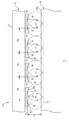
- FIG. 2 is a diagram illustrating a state in which the backlight device 20 according to the first embodiment is viewed from the viewpoint P in FIG.
- Each LED unit 34 has a package 50 and two LEDs 38.
- the package 50 is formed in a plate shape whose outer shape is rectangular by a semiconductor with high heat dissipation.
- the package 50 is formed in a shape in which both ends in the longitudinal direction are raised and the center is recessed.
- the concave bottom 50a is flat.
- the two LEDs 38 are juxtaposed in the longitudinal direction on the bottom 50a at the first arrangement interval P1.
- the package 50 is provided with inclined portions 50b at both ends in the longitudinal direction in order to efficiently use the light emitted from the side surface of the LED 38.
- the inclined portion 50b is formed to be higher than the LED 38. Further, the surface of the package 50 is formed so that the reflectance is high. By providing the inclined portion 50b in this way, light can be incident at an angle closer to the vertical from the LED 38 toward the end surface 22a. In addition, the light emitted from the LED 38 and traveling at a large angle from the direction perpendicular to the light guide plate 22 is blocked by the inclined portion 50b.
- the two LEDs 38 provided in one LED unit 34 are integrally formed.
- the number of LEDs 38 provided in the LED unit 34 is not limited to two, and three or more LEDs 38 such as 3, 4, 6, 8 may be provided. Even in this case, the plurality of LEDs 38 provided in the same LED unit 34 are arranged in parallel at equal intervals with the first arrangement interval P1.
- a plurality of LED units 34 are juxtaposed in the extending direction of the end face 22a of the light guide plate 22 at a second arrangement interval P2.
- a plurality of LED units 34 are arranged in parallel so that the extending direction of the end face 22 a and the parallel direction of the LEDs 38 in each LED unit 34 form a right angle. Is also possible.
- the light guide plate 22 is also thin. For this reason, when LED38 is arrange
- the plurality of LED units 34 are arranged such that the LEDs 38 are arranged in a straight line in the extending direction of the end face 22a.
- the first arrangement interval P1 is 0.6 mm
- the second arrangement interval P2 is 10 mm.
- the first arrangement interval P1 and the second arrangement interval P2 are not limited to this value.
- the first arrangement interval P1 needs to be at least 0.1 mm in order to arrange the first arrangement interval P1 so as not to overlap in the pitch direction.
- the mounting cost can be reduced by enabling one ceramic package to be mounted on a substrate by an automatic machine.
- interval P1 needs to be 3 mm or less, and 2 mm is made into the preferable value.
- the first arrangement interval P1 may be any value between 0.1 mm and 3 mm.
- the second arrangement interval P2 may be any value between 5 mm and 15 mm.
- the LED unit 34 is provided with one anode electrode and one cathode electrode.
- the pair of electrodes is used as a common electrode. When a voltage is applied between the electrodes, both the two LEDs 38 of the LED unit 34 are turned on. The two LEDs 38 are connected in parallel, and a protection element for protection from overvoltage is also connected in parallel.
- the thin light guide plate 22 When the thin light guide plate 22 is employed, it is difficult to arrange the LEDs 38 in parallel with the extending direction of the light guide plate 22 as described above. For this reason, in order to avoid the shortage of the amount of light incident on the light guide plate 22, it is conceivable to arrange a large number of LEDs 38 by reducing the arrangement interval of the LEDs 38. However, when an electrode is provided for each LED 38, the mounting operation of the LED 38 becomes complicated, and it may be difficult to suppress the number of manufacturing steps of the image display device 10.
- the plurality of LEDs 38 can be integrally attached to the LED 38 by attaching the LED unit 34 to the flexible substrate 32. Therefore, the LED 38 can be easily attached and the manufacturing process of the image display device 10 can be simplified.
- LED38 it is not limited to the aspect in which several LED38 is comprised integrally in this way,
- a pair of electrode to which a voltage is applied at the time of lighting may be provided in each LED38.
- the plurality of LEDs 38 are not integrally configured, and the arrangement interval of the LEDs 38 in the group constituted by two or more LEDs 38 is the first arrangement interval P1, and the arrangement interval of the group is the second arrangement interval. You may arrange in parallel so that it may become P2.
- group refers to a plurality of LED groups arranged at equal intervals in the first arrangement interval P1.
- the number of LEDs included in the group is not limited to two, and may be three or more, such as 3, 4, 6, 8, for example.
- the plurality of LEDs 38 may be arranged such that N ⁇ the first arrangement interval P1 ⁇ the second arrangement interval P2, where N is the number of LEDs included in each group.
- the LED 38 functions as a point light source. It is known that the distribution D of light emitted from each LED 38 is circular as shown in FIG. For this reason, light intensity unevenness due to the arrangement interval of the LEDs 38 may occur in the light incident on the end surface 22 a of the light guide plate 22.
- “light intensity unevenness” refers to the difference between the maximum value and the minimum value of the light intensity on the end surface 22 a of the light guide plate 22.
- the component in the direction parallel to the end surface 22a is stronger than the direction perpendicular to the end surface 22a of the light guide plate 22. Such a light intensity distribution can contribute to further increasing the light intensity unevenness.
- the light intensity unevenness increases and decreases as the interval H is changed.
- the distance from the LED to the light guide plate becomes shorter, the decrease in luminous intensity between the LEDs increases and the luminous intensity unevenness also increases.
- the interval H is required to be set so that the light intensity unevenness and the light intensity average at the end surface 22a of the light guide plate 22 satisfy the required values.
- the plurality of LEDs 38 are arranged so that the arrangement interval between the two LEDs 38 provided in the LED unit 34 is the first arrangement interval P1, and the arrangement interval of the LED units 34 is the second arrangement interval P2. It is installed. For this reason, increase / decrease in luminous intensity unevenness also varies depending on the first arrangement interval P1 and the second arrangement interval P2.
- FIG. 3 is a diagram showing a relationship between the interval H in the backlight device 20 according to the first embodiment and the light intensity unevenness K at the end face 22a of the light guide plate 22.
- interval P2 is 5 mm, 10 mm, and 15 mm is each shown.
- the broken lines shown when the second arrangement interval P2 is 5 mm and 15 mm indicate the fluctuation range when the first arrangement interval P1 is changed within the range of 0.1 mm to 3 mm.
- FIG. 3 shows that the light intensity unevenness K increases as the second arrangement interval P2 increases.
- the permissible limit light intensity unevenness Kmax is a limit value of the light intensity unevenness of the incident light on the end surface 22a of the light guide plate 22 that is allowed to satisfy the required quality of the image display device 10.
- the interval H is 4 mm, which is the minimum value for the light intensity unevenness K to be less than or equal to the allowable limit light intensity unevenness Kmax.
- the luminosity unevenness K is an allowable limit.
- the interval H needs to be 1 mm or more and 7 mm or less. Therefore, the light guide plate 22 is arranged so that the interval H is 1 mm or more and 7 mm or less.
- the first arrangement interval P1 is 0.5 mm
- the second arrangement interval P2 is 5 mm
- the interval H is 1.5 mm
- the first arrangement interval P1 is 0.6 mm
- the second arrangement interval P2 is 8 mm
- the interval H is 3 mm
- the first arrangement interval P1 is 0.7 mm
- the second arrangement interval P2 is 10 mm
- the interval H is 4 mm.
- the first arrangement interval P1 is 0.1 mm to 2 mm
- the interval H is 1 mm to 5 mm
- the second arrangement interval P2 is 5 mm to 11 mm.
- FIG. 4 is a front view schematically showing the backlight device 20 according to the first embodiment.
- the lower two corner portions are supported by the first support member 60, and the upper two corner portions are respectively supported by the second support member 62.
- the substrate unit 30 is provided so that the LEDs 38 face the upper end surface 22 a and the lower end surface 22 a of the light guide plate 22, respectively.
- the light guide plate 22 is positioned against the first support member 60 by gravity. For this reason, when the height L4 of the light guide plate 22 (hereinafter referred to as “light guide plate height L4”) expands or contracts due to the temperature of the installation environment, the distance H between the lower end surface 22a and the LED 38 does not change much. On the other hand, the distance H between the upper end face 22a and the LED 38 changes relatively greatly.
- the interval H increases when the light guide plate 22 contracts due to the decrease in the environmental temperature.
- the end surface 22a of the light guide plate 22 reaches the visual recognition boundary S2, and the end surface 22a of the light guide plate 22 may be visible from the virtual viewpoint S1.
- the end surface 22a of the light guide plate 22 is visually recognized through the periphery of the light shielding boundary S3. As a result, the surrounding area looks dark, which may give the user a feeling of strangeness.
- the end surface 22a of the light guide plate 22 is seen by the light shielding portion 12a when viewed from the virtual viewpoint S1 of the user.
- the virtual viewpoint S1 to the visual boundary S2 do not become a straight line due to the refractive indexes of the optical sheet 18 and the light guide plate 22, but it is assumed here that the virtual viewpoint S1 and the visual boundary S2 can be connected by a straight line.
- the visual boundary S2 is light-shielded by L2 which is L3 ⁇ tan ⁇ .
- the position is higher than the boundary S3.
- the image display device 10 has a standard environmental temperature Ts, which is a standard temperature in an environment where installation is assumed, set to 25 degrees.
- the light guide plate 22 is provided such that the distance from the end surface 22a of the light guide plate 22 to the visual recognition boundary S2 is the margin L1 at the standard environmental temperature Ts.
- the image display apparatus 10 is preliminarily set with an assumed environmental temperature that is a temperature range assumed in the environment in which the image display apparatus 10 is installed.
- the assumed environmental temperature is a temperature between the minimum environmental temperature Tmin and the maximum environmental temperature Tmax. It is said that.
- the margin L1 is set longer than the contraction amount of the light guide plate 22 when the environmental temperature decreases from the standard environmental temperature Ts to the minimum environmental temperature Tmin. Thereby, even when the minimum environmental temperature Tmin is reached, the end face 22a is prevented from reaching the visual recognition boundary S2.
- the light guide plate 22 is provided so that the interval H does not become shorter than the minimum interval Hmin at which the unevenness in light intensity due to the arrangement interval of the plurality of LEDs 38 becomes an allowable value even when the light guide plate 22 extends due to a temperature change within the assumed environmental temperature.
- the light guide plate 22 is provided so as to satisfy the first arrangement interval P1 ⁇ the interval H ⁇ the second arrangement interval P2 even when the light guide plate 22 expands and contracts due to a temperature change within the assumed environmental temperature.
- FIG. 5 is a diagram illustrating a relationship between the light guide plate height L4 and the change in the interval H in the backlight device 20 according to the first embodiment.
- the straight line rising to the right indicates the relationship between the light guide plate height L4 and the interval H when the environmental temperature reaches the minimum environmental temperature Tmin. Shows the relationship between the light guide plate height L4 and the distance H when the maximum ambient temperature Tmax is reached.
- the interval at the standard ambient temperature Ts is Hs.
- the linear expansion coefficient ⁇ of the light guide plate 22 is 6 ⁇ 10 ⁇ ⁇ 5 or more and 8 ⁇ 10 ⁇ ⁇ 5 or less.
- changes in light guide plate height L4 and interval H Shows the relationship.
- the maximum interval Hmax refers to the maximum value of the interval H at which the incident light efficiency of light incident on the end surface 22a of the light guide plate 22 from the LED 38 is an allowable value.
- H is provided so as not to be long.
- the minimum interval Hmin is the minimum value of the interval H at which the light intensity unevenness of light incident from the LED 38 to the end surface 22a of the light guide plate 22 is an allowable value, and satisfies the first arrangement interval P1 ⁇ the interval H as described above. This is the minimum value. Since this value is the first arrangement interval P1, in the first embodiment, the interval H is the same as the first arrangement interval P1.
- the light guide plate height L4 is not exceeded in order not to exceed the maximum interval Hmax even when the interval H increases due to the contraction of the light guide plate 22. It is understood that it is necessary to set the thickness to 800 mm or less.
- the light guide plate height L4 is similarly set to 800 mm or less in order not to exceed the minimum interval Hmin even when the interval H decreases due to the extension of the light guide plate 22. It is understood that it is necessary to. For this reason, also in 1st Embodiment, the light-guide plate height L4 shall be 800 mm or less.
- the maximum interval Hmax in FIG. 5 indicates that the end surface 22a of the light guide plate 22 is shielded from the liquid crystal panel 12 when viewed from the virtual viewpoint S1 of the user even when the light guide plate 22 contracts to the maximum due to a temperature change within the assumed environmental temperature. It may be the maximum value of the interval H so as not to be seen by being blocked by the portion 12a. In this case, the value obtained by adding the interval H and the margin L1 at the standard environment temperature Ts needs to be equal to or less than the maximum interval Hmax.
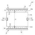
- FIG. 6 is a block diagram schematically showing the configuration of the lighting control system 70 provided in the backlight device 20 according to the first embodiment.
- the lighting control system 70 includes an LED drive control circuit 72, an LED drive circuit 74, an LED 38, and a temperature sensor 76.
- the temperature sensor 76 is provided in the image display device 10 and detects the environmental temperature around the light guide plate 22.
- the temperature sensor 76 is connected to the LED drive control circuit 72, and the LED drive control circuit 72 reads the detection result of the temperature sensor 76 every predetermined time.
- the LED drive control circuit 72 sends a control signal to the LED drive circuit 74, and the LED drive circuit 74 supplies a drive current corresponding to the received control signal to the LED 38.
- the light guide plate 22 is made of acrylic having a standard environment temperature Ts of 25 ° C., a maximum environment temperature Tmax of 50 ° C., and a linear expansion coefficient ⁇ of 8 ⁇ 10 ⁇ -5, and the light guide plate height L4 is 400 mm.
- the maximum environmental temperature Tmax is 4.0 mm.
- the lighting control system 70 controls the electric power given to the LED 38 so as to suppress the fluctuation of the light intensity of the irradiation light from the backlight device 20 to the liquid crystal panel 12 due to such a change in incident light efficiency.
- the LED drive control circuit 72 reduces the drive current supplied to the LED 38 as the environmental temperature around the light guide plate 22 detected by the temperature sensor 76 increases, and the environment around the light guide plate 22.
- the power supply to the LED 38 is controlled to increase the drive current supplied to the LED 38 as the temperature decreases. For example, when the x% temperature rises with respect to the standard environment temperature Ts, the LED drive control circuit 72 decreases the drive current supplied to the LED 38 by a ⁇ x% with a being a constant. Conversely, when the x% temperature falls with respect to the standard environment temperature Ts, the drive current supplied to the LED 38 is increased by a ⁇ x%. Thereby, since LED38 can be lighted efficiently, the power consumption by LED38 can be reduced and the emitted-heat amount from LED38 can be suppressed.
- the LED drive control circuit 72 may hold a table that defines the correspondence between the output value of the temperature sensor 76 and the drive current to be supplied to the LED 38.
- the LED drive control circuit 72 may determine the drive current to be supplied to the LED 38 with reference to this table.
- FIG. 7 is a front view schematically showing the backlight device 100 according to the second embodiment.
- the backlight device 100 includes the backlight device 20 according to the first embodiment, except that the light guide plate 102 and the support member 104 are provided in place of the light guide plate 22, the first support member 60, and the second support member 62. It is comprised similarly.
- the same parts as those in the first embodiment are denoted by the same reference numerals and description thereof is omitted.
- the light guide plate 102 is provided with a rectangular groove 102b substantially at the center of the left and right end faces.
- Two support members 104 are fixed to the rear plate 24.
- the support member 104 has a rectangular outer shape having a height slightly smaller than the groove 102b.
- the light guide plate 102 is disposed such that the support member 104 is inserted into the groove 102b. In this way, the light guide plate 102 is positioned at the approximate center in the direction L4 of the light guide plate by the support member 104.
- the shape of the groove 102b and the support member 104 is not limited to a rectangle.
- the upper and lower intervals H are set.
- the fluctuation can be suppressed to about half.
- the positioning of the light guide plate 102 is not limited to the substantially central position in the height direction, and the light guide plate 102 may be positioned in other midway portions on the left and right end surfaces of the light guide plate 102.
- 10 image display device 12 liquid crystal panel, 12a shading part, 13 front cover, 14 chassis, 20 backlight device, 22 light guide plate, 22a end face, 23 dot pattern, 24 rear plate, 26 heat sink, 30 substrate unit, 32 flexible substrate 34 LED unit, 38 LED, 40 reflection sheet, 42 light mixing chamber, 50 package, 50a bottom part, 50b inclined part, 60 first support member, 62 second support member, 70 lighting control system, 72 LED drive control circuit, 74 LED drive circuit, 76 temperature sensor, 100 backlight device, 102 light guide plate, 102a end face.
- the present invention can be used in a backlight device, and in particular, can be used in a backlight device that emits light from the back surface of an image display panel.
Landscapes
- Physics & Mathematics (AREA)
- General Physics & Mathematics (AREA)
- Optics & Photonics (AREA)
- Engineering & Computer Science (AREA)
- Microelectronics & Electronic Packaging (AREA)
- Planar Illumination Modules (AREA)
Abstract
Description
図1は、第1の実施形態に係る画像表示装置10の断面図である。図1は、装置左右方向に垂直な平面で切断したときの画像表示装置10の上方の部分の断面を示している。画像表示装置10は、液晶パネル12、フロントカバー13、シャーシ14、クッション16、光学シート18、およびバックライト装置20を有する。
アクリル:α=7~8×10^-5[/℃]
ポリカーボネ-ト:α=6~7×10^-5[/℃]
となる。このため、導光板22の線膨張係数αは、6×10^-5以上8×10^-5以下とする。図5では、線膨張係数αが6×10^-5、7×10^-5、および8×10^-5の3種類の導光板22について、導光板高さL4と間隔Hの変化との関係を示している。
図7は、第2の実施形態に係るバックライト装置100を模式的に示した正面図である。バックライト装置100は、導光板22、第1支持部材60、および第2支持部材62に代えて導光板102および支持部材104が設けられる以外は、第1の実施形態に係るバックライト装置20と同様に構成される。以下、第1の実施形態と同様の個所については同一の符号を付して説明を省略する。
Claims (5)
- 導光板と、
前記導光板の端面と間隔Hを介して前記導光板の端面の延在方向に並設された複数の白色発光ダイオードと、
を備え、
前記複数の白色発光ダイオードは、2以上の白色発光ダイオードによってグループが構成され、前記グループにおける白色発光ダイオードの配置間隔がP1となり、且つグループの配置間隔がP2となるよう並設され、
前記導光板は、P1≦H≦P2を満たすよう配置されることを特徴とするバックライト装置。 - 前記複数の白色発光ダイオードは、前記P1が0.1mm以上3mm以下、および前記P2が5mm以上15mm以下を満たすよう並設され、
前記導光板は、前記Hが1mm以上7mm以下となるよう配置されることを特徴とする請求項1に記載のバックライト装置。 - 前記導光板は、厚さが1mm以上5mm以下であることを特徴とする請求項1または2に記載のバックライト装置。
- 前記グループの各々に含まれる2以上の白色発光ダイオードは、一体的に構成されていることを特徴とする請求項1から3のいずれかに記載のバックライト装置。
- 前記複数の白色発光ダイオードは、各々のグループに含まれる白色発光ダイオードの数をNとして、N×P1<P2となるよう配置されることを特徴とする請求項1から4のいずれかに記載のバックライト装置。
Priority Applications (6)
| Application Number | Priority Date | Filing Date | Title |
|---|---|---|---|
| KR1020117026839A KR101353194B1 (ko) | 2009-04-13 | 2010-04-05 | 백라이트 장치 |
| EP10764226.6A EP2420724B1 (en) | 2009-04-13 | 2010-04-05 | Backlight device |
| CN201080016713.7A CN102395826B (zh) | 2009-04-13 | 2010-04-05 | 背光灯装置 |
| US13/264,352 US8596850B2 (en) | 2009-04-13 | 2010-04-05 | Backlight device |
| US14/060,442 US8807818B2 (en) | 2009-04-13 | 2013-10-22 | Backlight device |
| US14/328,555 US9389357B2 (en) | 2009-04-13 | 2014-07-10 | Backlight device |
Applications Claiming Priority (2)
| Application Number | Priority Date | Filing Date | Title |
|---|---|---|---|
| JP2009097471A JP5267298B2 (ja) | 2009-04-13 | 2009-04-13 | バックライト装置 |
| JP2009-097471 | 2009-04-13 |
Related Child Applications (2)
| Application Number | Title | Priority Date | Filing Date |
|---|---|---|---|
| US13/264,352 A-371-Of-International US8596850B2 (en) | 2009-04-13 | 2010-04-05 | Backlight device |
| US14/060,442 Continuation US8807818B2 (en) | 2009-04-13 | 2013-10-22 | Backlight device |
Publications (1)
| Publication Number | Publication Date |
|---|---|
| WO2010119639A1 true WO2010119639A1 (ja) | 2010-10-21 |
Family
ID=42982314
Family Applications (1)
| Application Number | Title | Priority Date | Filing Date |
|---|---|---|---|
| PCT/JP2010/002485 WO2010119639A1 (ja) | 2009-04-13 | 2010-04-05 | バックライト装置 |
Country Status (6)
| Country | Link |
|---|---|
| US (3) | US8596850B2 (ja) |
| EP (1) | EP2420724B1 (ja) |
| JP (1) | JP5267298B2 (ja) |
| KR (1) | KR101353194B1 (ja) |
| CN (1) | CN102395826B (ja) |
| WO (1) | WO2010119639A1 (ja) |
Cited By (3)
| Publication number | Priority date | Publication date | Assignee | Title |
|---|---|---|---|---|
| US20120162875A1 (en) * | 2010-12-27 | 2012-06-28 | Kabushiki Kaisha Toshiba | Television and electronic apparatus |
| WO2012075384A3 (en) * | 2010-12-04 | 2012-09-27 | 3M Innovative Properties Company | Illumination assembly and method of forming same |
| US9270924B2 (en) | 2010-12-27 | 2016-02-23 | Kabushiki Kaisha Toshiba | Television and electronic apparatus |
Families Citing this family (12)
| Publication number | Priority date | Publication date | Assignee | Title |
|---|---|---|---|---|
| JP5267298B2 (ja) * | 2009-04-13 | 2013-08-21 | 株式会社Jvcケンウッド | バックライト装置 |
| US8770819B2 (en) * | 2010-07-12 | 2014-07-08 | Sharp Kabushiki Kaisha | Surface light-emitting device and display device |
| WO2012070442A1 (ja) * | 2010-11-25 | 2012-05-31 | シャープ株式会社 | 照明装置、及び表示装置 |
| TW201400937A (zh) * | 2012-06-22 | 2014-01-01 | Wistron Corp | 背光模組及其顯示設備 |
| KR102013161B1 (ko) * | 2012-08-20 | 2019-08-23 | 삼성디스플레이 주식회사 | 백라이트 어셈블리 및 이를 갖는 표시 장치 |
| KR20140039425A (ko) * | 2012-09-21 | 2014-04-02 | 삼성디스플레이 주식회사 | 표시장치 |
| US9599764B2 (en) * | 2013-01-09 | 2017-03-21 | Sharp Kabushiki Kaisha | Illumination device, display device and TV receiver |
| JP2015082017A (ja) * | 2013-10-22 | 2015-04-27 | 株式会社ジャパンディスプレイ | 液晶表示装置 |
| JP2015129818A (ja) * | 2014-01-06 | 2015-07-16 | パナソニック液晶ディスプレイ株式会社 | 液晶表示装置 |
| EP3259051B1 (en) * | 2015-02-17 | 2022-05-04 | Vita-Mix Management Corporation | Interlocking blending system |
| US11253106B2 (en) | 2015-04-24 | 2022-02-22 | Vita-Mix Management Corporation | Interlocking blending system |
| WO2016172682A1 (en) | 2015-04-24 | 2016-10-27 | Vita-Mix Management Corporation | Interlocking blending system |
Citations (2)
| Publication number | Priority date | Publication date | Assignee | Title |
|---|---|---|---|---|
| JP2003532270A (ja) | 2000-05-04 | 2003-10-28 | コーニンクレッカ フィリップス エレクトロニクス エヌ ヴィ | 照明装置、光混合チャンバ及び表示装置 |
| JP2007234412A (ja) | 2006-03-01 | 2007-09-13 | Matsushita Electric Ind Co Ltd | エッジ入力型バックライトおよび液晶表示装置 |
Family Cites Families (25)
| Publication number | Priority date | Publication date | Assignee | Title |
|---|---|---|---|---|
| JPH10319217A (ja) * | 1997-05-22 | 1998-12-04 | Omron Corp | 色分離素子及び画像表示装置 |
| JP2004079488A (ja) | 2002-08-22 | 2004-03-11 | Fujitsu Ten Ltd | Ledバックライトユニットおよび液晶表示装置 |
| US7455441B2 (en) | 2003-09-29 | 2008-11-25 | Panasonic Corporation | Linear light source, method for manufacturing the same and surface emitting device |
| JP4683874B2 (ja) | 2004-07-29 | 2011-05-18 | 京セラ株式会社 | 光源装置、および液晶表示装置 |
| JP2006134661A (ja) | 2004-11-04 | 2006-05-25 | Matsushita Electric Ind Co Ltd | 面状光源及びこれを用いた液晶表示装置 |
| EP1830415B1 (en) * | 2004-12-24 | 2017-01-25 | Kabushiki Kaisha Toshiba | White led, backlight using same and liquid crystal display |
| JP2006302762A (ja) * | 2005-04-22 | 2006-11-02 | Matsushita Electric Ind Co Ltd | エッジ入力型バックライト及び液晶表示装置 |
| KR20080033164A (ko) * | 2005-07-04 | 2008-04-16 | 마츠시타 덴끼 산교 가부시키가이샤 | 선형광원장치, 면 발광장치 및 액정표시장치 |
| JP2007059168A (ja) * | 2005-08-24 | 2007-03-08 | Matsushita Electric Ind Co Ltd | バックライト |
| CN100405165C (zh) * | 2005-09-05 | 2008-07-23 | 清华大学 | 背光系统及其反光罩 |
| CN100462811C (zh) * | 2006-02-10 | 2009-02-18 | 鸿富锦精密工业(深圳)有限公司 | 箱式光源模组和背光系统 |
| US7674030B2 (en) * | 2006-05-23 | 2010-03-09 | Avago Technologies General Ip (Singapore) Pte. Ltd. | Light source for even illumination of a light guide |
| WO2007138763A1 (ja) * | 2006-06-01 | 2007-12-06 | Sharp Kabushiki Kaisha | 面状光源装置及びこれを設けた液晶表示装置 |
| JP2008060204A (ja) * | 2006-08-30 | 2008-03-13 | Nec Lcd Technologies Ltd | Ledバックライトユニットおよびそれを用いた液晶表示装置 |
| KR101340437B1 (ko) * | 2006-09-25 | 2013-12-11 | 삼성디스플레이 주식회사 | 표시장치용 백커버, 이를 갖는 백라이트 어셈블리 및표시장치 |
| KR20080051236A (ko) * | 2006-12-05 | 2008-06-11 | 삼성전자주식회사 | 엘이디 패키지 및 그 엘이디 패키지를 포함하는 광원유닛및 백라이트 유닛 |
| US7661862B2 (en) * | 2006-12-07 | 2010-02-16 | Skc Haas Display Films Co., Ltd. | LCD display backlight using elongated illuminators |
| JP2008210691A (ja) * | 2007-02-27 | 2008-09-11 | Minebea Co Ltd | 面状照明装置 |
| JP2008305713A (ja) * | 2007-06-08 | 2008-12-18 | Fujifilm Corp | 面状照明装置 |
| JP2010020961A (ja) * | 2008-07-09 | 2010-01-28 | Citizen Electronics Co Ltd | 面状光源及び液晶表示装置 |
| JP5255960B2 (ja) * | 2008-09-04 | 2013-08-07 | 株式会社ジャパンディスプレイイースト | 液晶表示装置 |
| TW201035641A (en) * | 2009-03-19 | 2010-10-01 | Advanced Optoelectronic Tech | Backlight module |
| JP5267298B2 (ja) * | 2009-04-13 | 2013-08-21 | 株式会社Jvcケンウッド | バックライト装置 |
| TWI380096B (en) * | 2009-05-08 | 2012-12-21 | Au Optronics Corp | Backlight unit |
| KR20110000964A (ko) * | 2009-06-29 | 2011-01-06 | 삼성전자주식회사 | 액정 표시 장치 및 그 제조방법 |
-
2009
- 2009-04-13 JP JP2009097471A patent/JP5267298B2/ja active Active
-
2010
- 2010-04-05 WO PCT/JP2010/002485 patent/WO2010119639A1/ja active Application Filing
- 2010-04-05 CN CN201080016713.7A patent/CN102395826B/zh active Active
- 2010-04-05 EP EP10764226.6A patent/EP2420724B1/en active Active
- 2010-04-05 US US13/264,352 patent/US8596850B2/en active Active
- 2010-04-05 KR KR1020117026839A patent/KR101353194B1/ko active IP Right Grant
-
2013
- 2013-10-22 US US14/060,442 patent/US8807818B2/en active Active
-
2014
- 2014-07-10 US US14/328,555 patent/US9389357B2/en active Active
Patent Citations (2)
| Publication number | Priority date | Publication date | Assignee | Title |
|---|---|---|---|---|
| JP2003532270A (ja) | 2000-05-04 | 2003-10-28 | コーニンクレッカ フィリップス エレクトロニクス エヌ ヴィ | 照明装置、光混合チャンバ及び表示装置 |
| JP2007234412A (ja) | 2006-03-01 | 2007-09-13 | Matsushita Electric Ind Co Ltd | エッジ入力型バックライトおよび液晶表示装置 |
Non-Patent Citations (1)
| Title |
|---|
| See also references of EP2420724A4 |
Cited By (4)
| Publication number | Priority date | Publication date | Assignee | Title |
|---|---|---|---|---|
| WO2012075384A3 (en) * | 2010-12-04 | 2012-09-27 | 3M Innovative Properties Company | Illumination assembly and method of forming same |
| CN103238092A (zh) * | 2010-12-04 | 2013-08-07 | 3M创新有限公司 | 照明组件及其形成方法 |
| US20120162875A1 (en) * | 2010-12-27 | 2012-06-28 | Kabushiki Kaisha Toshiba | Television and electronic apparatus |
| US9270924B2 (en) | 2010-12-27 | 2016-02-23 | Kabushiki Kaisha Toshiba | Television and electronic apparatus |
Also Published As
| Publication number | Publication date |
|---|---|
| JP2010251026A (ja) | 2010-11-04 |
| US20140043564A1 (en) | 2014-02-13 |
| EP2420724A4 (en) | 2018-01-24 |
| US8807818B2 (en) | 2014-08-19 |
| US20140320785A1 (en) | 2014-10-30 |
| JP5267298B2 (ja) | 2013-08-21 |
| CN102395826B (zh) | 2014-04-16 |
| CN102395826A (zh) | 2012-03-28 |
| US9389357B2 (en) | 2016-07-12 |
| KR101353194B1 (ko) | 2014-01-17 |
| KR20120001802A (ko) | 2012-01-04 |
| US20120134174A1 (en) | 2012-05-31 |
| US8596850B2 (en) | 2013-12-03 |
| EP2420724B1 (en) | 2022-08-31 |
| EP2420724A1 (en) | 2012-02-22 |
Similar Documents
| Publication | Publication Date | Title |
|---|---|---|
| JP5267298B2 (ja) | バックライト装置 | |
| KR101484662B1 (ko) | 면 발광 유닛 및 그를 구비한 표시 장치 | |
| US8757860B2 (en) | Backlight device, liquid crystal display device and television receiver | |
| KR102216100B1 (ko) | 표시장치 | |
| WO2011043140A1 (ja) | 照明装置、表示装置、及びテレビ受信装置 | |
| JP2010092670A (ja) | 照明装置及び画像表示装置 | |
| KR20170083248A (ko) | 디스플레이 디바이스 | |
| KR20140020446A (ko) | 백라이트 어셈블리 및 이를 갖는 표시 장치 | |
| KR101318933B1 (ko) | 백라이트 장치, 화상 표시 장치 및 백라이트 장치의 조립 방법 | |
| KR20140004881A (ko) | 백라이트 유닛 | |
| JP2010251027A (ja) | バックライト装置 | |
| KR20160093182A (ko) | 표시장치 및 이의 제조방법 | |
| JP5527230B2 (ja) | バックライト装置及び画像表示装置 | |
| JP5345361B2 (ja) | 表示装置及び発光装置 | |
| KR20130022980A (ko) | 발광 다이오드 광원 및 이를 구비한 백라이트 유닛 | |
| WO2012102096A1 (ja) | エッジライト型照明装置及び表示装置 | |
| JP7504093B2 (ja) | 線状発光装置 | |
| JP2012154970A (ja) | 液晶モジュール | |
| KR102476469B1 (ko) | 광원 모듈 및 이를 포함하는 표시 장치 | |
| US20190265405A1 (en) | Illumination device and display device | |
| KR101956726B1 (ko) | 백라이트 유닛 및 이를 구비한 액정표시장치 | |
| KR101971617B1 (ko) | 백라이트 유닛 | |
| KR102005478B1 (ko) | 조명장치 | |
| KR101232180B1 (ko) | 백라이트 유닛 및 이를 사용한 액정표시장치 | |
| KR20130027228A (ko) | 발광 다이오드 광원 및 이를 구비한 백라이트 유닛 |
Legal Events
| Date | Code | Title | Description |
|---|---|---|---|
| WWE | Wipo information: entry into national phase |
Ref document number: 201080016713.7 Country of ref document: CN |
|
| 121 | Ep: the epo has been informed by wipo that ep was designated in this application |
Ref document number: 10764226 Country of ref document: EP Kind code of ref document: A1 |
|
| DPE1 | Request for preliminary examination filed after expiration of 19th month from priority date (pct application filed from 20040101) | ||
| NENP | Non-entry into the national phase |
Ref country code: DE |
|
| ENP | Entry into the national phase |
Ref document number: 20117026839 Country of ref document: KR Kind code of ref document: A |
|
| WWE | Wipo information: entry into national phase |
Ref document number: 2010764226 Country of ref document: EP |
|
| WWE | Wipo information: entry into national phase |
Ref document number: 13264352 Country of ref document: US |