WO2010119503A1 - 有機エレクトロルミネッセンス素子およびその製造方法 - Google Patents
有機エレクトロルミネッセンス素子およびその製造方法 Download PDFInfo
- Publication number
- WO2010119503A1 WO2010119503A1 PCT/JP2009/057484 JP2009057484W WO2010119503A1 WO 2010119503 A1 WO2010119503 A1 WO 2010119503A1 JP 2009057484 W JP2009057484 W JP 2009057484W WO 2010119503 A1 WO2010119503 A1 WO 2010119503A1
- Authority
- WO
- WIPO (PCT)
- Prior art keywords
- organic
- layer
- transport layer
- light emitting
- electron
- Prior art date
- Legal status (The legal status is an assumption and is not a legal conclusion. Google has not performed a legal analysis and makes no representation as to the accuracy of the status listed.)
- Ceased
Links
Images
Classifications
-
- H—ELECTRICITY
- H10—SEMICONDUCTOR DEVICES; ELECTRIC SOLID-STATE DEVICES NOT OTHERWISE PROVIDED FOR
- H10K—ORGANIC ELECTRIC SOLID-STATE DEVICES
- H10K50/00—Organic light-emitting devices
- H10K50/10—OLEDs or polymer light-emitting diodes [PLED]
- H10K50/17—Carrier injection layers
- H10K50/171—Electron injection layers
-
- H—ELECTRICITY
- H10—SEMICONDUCTOR DEVICES; ELECTRIC SOLID-STATE DEVICES NOT OTHERWISE PROVIDED FOR
- H10K—ORGANIC ELECTRIC SOLID-STATE DEVICES
- H10K50/00—Organic light-emitting devices
- H10K50/10—OLEDs or polymer light-emitting diodes [PLED]
- H10K50/14—Carrier transporting layers
-
- H—ELECTRICITY
- H10—SEMICONDUCTOR DEVICES; ELECTRIC SOLID-STATE DEVICES NOT OTHERWISE PROVIDED FOR
- H10K—ORGANIC ELECTRIC SOLID-STATE DEVICES
- H10K50/00—Organic light-emitting devices
- H10K50/80—Constructional details
- H10K50/805—Electrodes
- H10K50/82—Cathodes
- H10K50/828—Transparent cathodes, e.g. comprising thin metal layers
-
- H—ELECTRICITY
- H10—SEMICONDUCTOR DEVICES; ELECTRIC SOLID-STATE DEVICES NOT OTHERWISE PROVIDED FOR
- H10K—ORGANIC ELECTRIC SOLID-STATE DEVICES
- H10K71/00—Manufacture or treatment specially adapted for the organic devices covered by this subclass
-
- H—ELECTRICITY
- H10—SEMICONDUCTOR DEVICES; ELECTRIC SOLID-STATE DEVICES NOT OTHERWISE PROVIDED FOR
- H10K—ORGANIC ELECTRIC SOLID-STATE DEVICES
- H10K2102/00—Constructional details relating to the organic devices covered by this subclass
- H10K2102/301—Details of OLEDs
- H10K2102/302—Details of OLEDs of OLED structures
- H10K2102/3023—Direction of light emission
- H10K2102/3026—Top emission
Definitions
- An object of the present invention is to provide an organic electroluminescence element (hereinafter also referred to as an organic EL element) and a method for producing the same.
- an organic EL element an organic electroluminescence element
- This organic EL element is applicable to flat panel displays and illumination light sources, in particular, active matrix (AM) driven organic EL displays and organic EL lighting.
- organic EL elements can achieve high current density at low voltage, they can realize high luminance and luminous efficiency.
- application to flat panel displays such as liquid crystal displays has already been put into practical use. It is also expected as a light source.
- This organic EL element includes at least an organic EL layer including a light emitting layer, and an anode and a cathode sandwiching the organic EL layer.
- the electrode on the light extraction side is required to have a high transmittance with respect to EL light from the light emitting layer.
- transparent conductive oxide materials such as indium-tin oxide (ITO), indium-zinc oxide (IZO), indium-tungsten oxide (IWO) are usually used. Used. Since these transparent conductive oxide materials have a relatively large work function of about 5 eV, they are used as hole injection electrodes (anodes) for organic materials.
- the light emission of the organic EL element is a hole injected into the highest occupied molecular orbital (HOMO, generally measured as an ionization potential) of the light emitting layer material, and the lowest unoccupied molecular orbital (LUMO, generally measured as an electron affinity). It is obtained by emitting light when the excitation energy of the excitons generated by recombination of electrons injected into the base relaxes.
- HOMO highest occupied molecular orbital
- LUMO lowest unoccupied molecular orbital
- an anode made of ITO is formed as a lower electrode on a transparent support substrate, and a hole injection / transport layer, a light emitting layer, an electron injection / transport layer, etc. are sequentially formed thereon as an organic EL layer.
- An organic EL element of a type (bottom emission type) in which a cathode made of a metal film such as Al is formed as an upper electrode and light is extracted from the support substrate side is common.
- a switching element by a thin film transistor (TFT) made of amorphous Si or poly Si is provided for each pixel, and an organic EL is formed thereon.
- TFT thin film transistor
- the switching element since the switching element is opaque, there is a problem that the aperture ratio (light emitting area) of the pixel is lowered.
- an organic EL element of a type (top emission type) in which the upper electrode is made transparent and light is extracted from the film formation surface side As a means for preventing a decrease in the aperture ratio of the pixel, it is desirable to apply an organic EL element of a type (top emission type) in which the upper electrode is made transparent and light is extracted from the film formation surface side.
- Non-Patent Document 1 a method in which an electron injection / transport layer, a light emitting layer, and a hole injection / transport layer are sequentially formed on the lower reflective electrode as a cathode, and an upper transparent electrode is used as an anode.
- the lower electrode is generally used as an anode from the viewpoint of the configuration of the switching circuit, and there is a high need for using the upper transparent electrode as a cathode.
- a metal thin film such as an Mg—Ag alloy may be used for the upper transparent cathode.
- the upper transparent electrode using a metal thin film has a problem that the emission intensity is lowered because the metal absorbs a considerable amount of visible light, and the lower reflective electrode has a microcavity effect due to its high reflectivity.
- the film thickness distribution of the organic layer which determines the distance between the metal thin film and the metal thin film, very precisely. Therefore, it is desired to use the transparent conductive oxide material conventionally used for the anode as the upper transparent cathode.
- the transparent conductive oxide material when the transparent conductive oxide material is deposited on the organic EL layer by a sputtering method or the like, the light emitting layer material and / or the electron injecting and transporting material made of an organic substance may be easily oxidized. Oxidation of these materials may deteriorate their functions and significantly impair the luminous efficiency of the organic EL element.
- Non-Patent Document 1 As a method for solving the problem of deterioration due to oxidation of the organic EL layer, a method of providing a damage mitigating layer between an electrode made of a transparent conductive oxide material and an electron transport layer has been conventionally used.
- the damage mitigating layer a very thin film of Mg—Ag alloy that has been used as a cathode material (see Non-Patent Document 1) and a copper phthalocyanine (CuPc) thin film (see Non-Patent Document 3) have been proposed.
- Patent Document 1 a method for preventing damage caused by sputtering by providing an electron injection layer made of an inorganic material on the electron transport layer has also been proposed (see Patent Document 1).
- Patent Documents 2-7 a method of applying a hole injection / transport layer and / or an electron injection / transport layer made of an inorganic semiconductor to a charge injection / transport layer of an organic EL element has been proposed (Patent Documents 2-7).
- the techniques described in Patent Documents 2-7 have been proposed in view of the following problems of organic EL elements at that time.
- Organic semiconductors are intrinsic semiconductors and have a very low charge density compared to inorganic semiconductors.
- the organic semiconductor has a small charge mobility, its electrical conductivity is low, and it is necessary to increase the driving voltage of the organic EL element. -Since the heat resistance of the organic semiconductor material is low, reliability and / or thermal stability is lacking.
- the inorganic semiconductor layer When the inorganic semiconductor layer is applied to a top emission type or a transparent organic EL element, the inorganic semiconductor layer is formed on the light extraction side when viewed from the light emitting layer, so that it is transparent to visible light, at least light emitted from the light emitting layer.
- SiC, SiN, aC (amorphous carbon), an oxide semiconductor, a II-VI group compound semiconductor, a III-V group compound semiconductor, and the like are preferably used.
- JP 2000-340364 A JP-A-62-76576 JP-A-1-312744 Japanese Patent Laid-Open No. 2-196475 Japanese Patent Laid-Open No. 3-77299 Japanese Patent Laid-Open No. 3-210792 Japanese Patent Laid-Open No. 11-149985
- Non-Patent Document 1 In the method using a metal thin film as the damage mitigating layer (Non-Patent Document 1), it is necessary to increase the thickness of the metal thin film in order to obtain a sufficient damage mitigating effect. However, increasing the thickness of the metal thin film raises the problem of absorbing light from the light emitting layer. Moreover, the method of using CuPc as the damage mitigating layer (Non-patent Document 3) reduces the problem of light absorption in the damage mitigating layer. However, since the electron injection property of CuPc into the electron transport layer is not sufficient, there are problems that the drive voltage of the device is increased and the light emission efficiency is lowered.
- the inorganic electron injection layer is formed of an alkali metal oxide or an alkaline earth metal oxide. Or an oxide of a lanthanoid element, and the electric conductivity of the inorganic electron injection layer itself is not high. Therefore, there is a trade-off problem between the effect of reducing the driving voltage of the element by reducing the film thickness and the effect of reducing the damage to the electron transport layer by increasing the film thickness. Further, depending on the forming method, there is a possibility that the organic electron transport layer adjacent to the inorganic electron injection layer may be oxidized and deteriorated.
- Patent Documents 2--7 when applied to a top emission type or transparent organic EL element, in the method using SiC, SiN, and aC as an inorganic semiconductor layer (Patent Documents 2-7), the formation is usually performed by plasma chemical vapor phase. A growth method (PECVD) or a sputtering method is used. Therefore, there is a problem that the organic EL layer including the light emitting layer is deteriorated by being exposed to plasma at the time of forming these inorganic semiconductor layers.
- PECVD plasma chemical vapor phase
- a sputtering method is used. Therefore, there is a problem that the organic EL layer including the light emitting layer is deteriorated by being exposed to plasma at the time of forming these inorganic semiconductor layers.
- the valence band which is the energy level of the conduction electron of the oxide semiconductor
- the valence band is the lowest unoccupied energy level of the conduction electron of the organic light emitting layer and the organic electron transport layer.
- LUMO molecular orbital
- the present invention has been made in view of the above-mentioned problems. Even when an upper cathode made of a transparent conductive oxide is formed by a sputtering method or the like, the organic functional layer is not oxidized and is highly efficient at a low driving voltage. It is to provide a top emission type or transparent organic EL element.
- an anode, an organic EL layer, and a cathode are provided in this order on a support substrate, and the organic EL layer includes at least a hole transport layer, a light emitting layer, and an electron transport layer from the anode side.
- An electron injection layer is provided in this order, and the hole transport material, the light emitting layer material, and the electron transport material are organic materials, and the cathode is a transparent conductive oxide.
- the injection layer is made of an n-type chalcogenide semiconductor having an optical band gap of 2.1 eV or more.
- an anode, an organic EL layer, and a cathode are provided on a support substrate in this order, and the organic EL layer is at least a hole transport layer, a light emitting layer,
- a method for producing an organic EL device comprising an electron transport layer and an electron injection layer in this order, wherein the hole transport material, the light emitting layer material, and the electron transport material are made of an organic material, and the cathode is made of a transparent conductive oxide.
- the electron injection layer made of the n-type chalcogenide semiconductor is formed by a physical vapor deposition method that does not use plasma discharge.
- an inorganic semiconductor layer made of an n-type chalcogenide semiconductor is formed between an electron transport layer made of an organic material and an upper cathode, so that a transparent conductive oxide is used as the upper cathode. Even if it is formed by sputtering, oxidation degradation of the light emitting layer or the electron transport layer is prevented. In addition, the light emitting layer and the electron transport layer are not deteriorated even when the inorganic semiconductor layer is formed.
- the n-type chalcogenide semiconductor electron injection layer efficiently draws electrons from the transparent oxide cathode, and the organic electron transport layer is disposed between the light emitting layer and the n-type chalcogenide semiconductor electron injection layer, thereby injecting electrons. It can alleviate the electron transport barrier from the light emitting layer to the light emitting layer and prevent hole injection from the light emitting layer to the electron injection layer, and realize a low voltage, high efficiency top emission type or transparent organic EL device. It becomes possible.
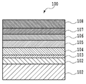
- FIG. 1 is a schematic view showing an example of the organic EL element of the present invention.
- FIG. 1 is a schematic diagram showing an example of the configuration of the organic EL element 100 of the present invention.
- an anode 102, a hole injection layer 103, a hole transport layer 104, a light emitting layer 105, an electron transport layer 106, an electron injection layer 107, and a cathode 108 are laminated on a substrate 101 in this order.
- the layer structure is as follows. This layer structure is the same as the structure shown in the prior art.
- the organic EL element of the present invention is a top emission type or transparent organic EL element
- the cathode is light transmissive and is made of a transparent conductive oxide material.
- the anode is a transparent organic EL element made of a transparent conductive oxide material
- the anode is also light transmissive, and light emitted from the light emitting layer is visible from both the anode side and the cathode side.
- the hole injection layer 103 is provided to promote hole injection from the anode 102 to the hole transport layer 104, but the hole injection layer 103 is not necessarily required.
- the n-type chalcogenide semiconductor is also used for the electron injection layer 107. It is also conceivable that the electron injection layer 107 is formed directly on the substrate. In this case, however, problems such as an increase in drive voltage and a decrease in light emission efficiency often occur.
- the electron transport layer 106 adjacent to the light emitting layer 105 is 1) a function of efficiently injecting electrons into the light emitting layer 105, and 2) holes that move from the light emitting layer 105 toward the cathode 108. There are two demands for the function to prevent this. However, in the electron injection layer 107 using an n-type chalcogenide semiconductor, it is difficult to satisfy these functions at the same time.
- the electron transport layer 106 made of an organic substance between the light emitting layer 105 and the electron injection layer 107 made of an n-type chalcogenide semiconductor.
- the organic material forming the electron transport layer 106 can be selected from a variety of materials according to the light emitting layer material, as will be described in detail below, and solves problems such as a decrease in light emission efficiency and an increase in driving voltage. Is possible.
- Substrate 101 that can be used in the present invention is insulated on a plastic substrate such as a silicon substrate or polycarbonate, a plastic film, or a stainless steel foil in addition to an alkali glass substrate and a non-alkali glass substrate that are generally used in flat panel displays. What formed the film
- membrane etc. can be used.
- the substrate 101 does not need to be transparent.
- a transparent organic EL element it is necessary to use a light-transmitting substrate.
- the anode 102 used in the organic EL element of the present invention may be light transmissive or light reflective.
- ITO indium-tin oxide
- IZO indium-zinc oxide
- IWO indium-tungsten oxide
- AZO Al-doped
- Zinc oxide) and transparent conductive oxide materials such as GZO (Ga-doped zinc oxide) can be used.
- a highly conductive polymer material such as poly (3,4-ethylenedioxythiophene): poly (styrenesulfonate) (PEDOT: PSS) can be used.
- the anode 102 can be a light reflective metal material alone or a laminated structure of the above-mentioned transparent conductive oxide material and light reflective metal material. Further, a light reflection layer made of a metal film is formed on the substrate 101, and an anode 102 made of a transparent conductive oxide material is formed thereon via an insulating layer, so that the light reflection layer and the anode 102 are not electrically connected. It is good also as a structure.
- a highly reflective metal, amorphous alloy, microcrystalline alloy, or a laminate thereof can be used as the metal material for forming the light reflective anode 102 or the light reflective layer.
- High reflectivity metals include Al, Ag, Ta, Zn, Mo, W, Ni, Cr, and the like.
- High reflectivity amorphous alloys include NiP, NiB, CrP, CrB, and the like.
- High reflectivity microcrystalline alloys include NiAl, silver alloys and the like.
- the organic EL layer is formed by laminating a hole injection layer 103, a hole transport layer 104, a light emitting layer 105, an electron transport layer 106, and an electron injection layer 107 in this order from the anode 102 side. ing. As described above, the hole injection layer 103 may be optionally provided.
- the material that can be used for the hole injection layer 103 of the organic EL element in the present invention is generally used in an organic EL element or an organic TFT element such as a material having a triarylamine partial structure, a carbazole partial structure, or an oxadiazole partial structure. Hole transport materials that are used.
- N, N′-diphenyl-N, N′-bis (3-methylphenyl) -1,1′-biphenyl-4,4′-diamine TPD
- N, N, N ′ , N′-tetrakis (4-methoxyphenyl) -benzidine MeO-TPD
- 4,4 ', 4" -tris (3-methylphenylphenylamino) triphenylamine m-MTDATA
- the hole injection layer 103 can also be formed using a hole transporting material commercially available from each organic electronic material manufacturer.
- an electron-accepting dopant may be added to the hole injection layer 103 (p-type doping).
- the electron-accepting dopant include organic semiconductors such as tetracyanoquinodimethane derivatives, specifically 2,3,5,6-tetrafluoro-7,7,8,8-tetracyanoquinodimethane ( F 4 -TCNQ) or the like can be used.
- An inorganic semiconductor such as molybdenum oxide (MoO 3 ), tungsten oxide (WO 3 ), or vanadium oxide (V 2 O 5 ) can also be used as the electron-accepting dopant.
- the material that can be used for the hole transport layer 104 of the organic EL element in the present invention is a known material used for the hole transport material of the organic EL element or organic TFT as exemplified in the hole injection layer. Any one can be selected and used.
- HTL and the ionization potential Ip (EML) of the light emitting layer 105 are Wa ⁇ Ip (HIL) ⁇ Ip (HTL) ⁇ Ip (EML) It is preferable to satisfy the relationship.
- the material of the light emitting layer 105 can be selected according to a desired color tone. For example, in order to obtain light emission from blue to blue-green, fluorescent whitening such as benzothiazole, benzimidazole, and benzoxazole is possible. Agents, styrylbenzene compounds, aromatic dimethylidene compounds, and the like can be used.
- 9,10-di (2-naphthyl) anthracene ADN
- 4,4′-bis (2,2′-diphenylvinyl) biphenyl DPVBi
- 2-methyl-9,10, di (2-naphthyl) anthracene MADN
- 9,10-bis- (9,9-bis (n-propyl) fluoren-2-yl) anthracene ADF
- 9- ( 2-naphthyl) -10- (9,9-bis (n-propyl) -fluoren-2-yl) anthracene ADN
- 2-methyl-9,10, di (2-naphthyl) anthracene MADN
- 9,10-bis- (9,9-bis (n-propyl) fluoren-2-yl) anthracene ADF
- the light emitting layer 105 may be doped with a fluorescent dye, and a dye material used as a light emitting dopant can be selected according to a desired color tone.
- a dye material used as a light emitting dopant can be selected according to a desired color tone.
- conventionally known condensed ring derivatives such as perylene and rubrene, quinacridone derivatives, phenoxazone 660, 4- (dicyanomethylene) -2-methyl-6- (p-dimethylaminostyryl) ) -4H-pyran (DCM), 4- (dicyanomethylene) -6-methyl-2- [2- (julolidin 9-yl) ethyl] -4H-pyran (DCM2), 4- (dicyanomethylene) -2- Methyl-6- (1,1,7,7-tetramethyljulolidyl-9-enyl) -4H-pyran (DCJT), 4- (dicyanomethylene) -2-t-but
- a plurality of luminescent dopants can be added in the same luminescent layer material.
- the electron transport layer 106 provided between the light-emitting layer 105 and the electron injection layer 107 made of an n-type chalcogenide semiconductor is important for extracting the performance of the device.
- the electron transport layer 106 is preferably made of a material having excellent electron transport properties selected from generally known organic electron transport materials. Further, it is desirable that the electron affinity of the material constituting the electron transport layer 106 takes a value between the electron affinity of the material constituting the light emitting layer 105 and the electron affinity of the n-type chalcogenide semiconductor constituting the electron injection layer 107. Further, the ionization potential Ip (ETL) of the electron transport layer 106 is desirably larger than the ionization potential Ip (EML) of the light emitting layer 105.
- a triazole derivative such as 3-phenyl-4- (1′-naphthyl) -5-phenyl-1,2,4-triazole (TAZ); -Bis [(4-tert-butylphenyl) -1,3,4-oxadiazole] phenylene (OXD-7), 2- (4-biphenylyl) -5- (4-tert-butylphenyl) -1, Oxadiazole derivatives such as 3,4-oxadiazole (PBD), 1,3,5-tris (4-tert-butylphenyl-1,3,4-oxadiazolyl) benzene (TPOB); -Thiophene derivatives such as bis (dimesitylboryl) -2,2'-bithiophene (BMB-2T), 5,5'-bis (dimesitylboryl) -2,2 ': 5'2'-terthiophene (BMB-3T
- an inorganic semiconductor layer made of an n-type chalcogenide semiconductor is used for the electron injection layer 107.
- the cathode 108 provided on the electron injection layer 107 is made of a transparent conductive oxide material, and is formed by a sputtering method or a reactive plasma film formation method.
- the electron transport layer 106 made of an organic substance adjacent to the electron injection layer 107 or the light emitting layer 105 is not damaged by the sputtering method or the plasma film formation method when the cathode 108 is formed.
- oxidative degradation of the organic layers (the electron transport layer 106 and the light emitting layer 105) can be prevented.
- a chalcogenide semiconductor is selected from inorganic semiconductors as the electron injection layer 107.
- the organic layer can be protected at the time of forming the cathode by using inorganic materials such as Si, SiC, SiN, III-V semiconductors, and amorphous carbon (aC).
- inorganic materials such as Si, SiC, SiN, III-V semiconductors, and amorphous carbon (aC).
- aC amorphous carbon
- an oxide semiconductor that can be formed by an evaporation method or the like may be used as the electron injection layer 107.
- the oxide semiconductor has an electron transport potential barrier at the interface between the electron injection layer 107 and the electron transport layer 106.
- the driving voltage is increased due to the increase in the thickness of the organic layer, and the underlying organic layer is oxidized and deteriorated by oxygen during formation.
- an n-type chalcogenide semiconductor can be formed by 1) hardly causing oxidation of the underlying organic layer when forming the electron injection layer, and 2) without using a plasma process and heating the substrate. ) Many of them have shallower conduction band levels than oxides, and are easily matched with LUMO of the organic electron transport layer.
- the electronegativity of the metal elements constituting the chalcogenide semiconductor for example, S, Se, and Te are 2.58, 2.55, and 2.1, respectively, which is lower than 3.44 of O. . Therefore, it is difficult to cause oxidative deterioration of the organic layer serving as a base, and characteristic deterioration of the organic EL element can be prevented.
- the electron transport layer 106 made of an adjacent organic material or the electron injection layer 107 having excellent electron injection properties to the light emitting layer 105 can be obtained.
- an n-type chalcogenide semiconductor is used as the electron injection layer 107 in the present invention.
- n-type chalcogenide semiconductors used in solar cells and the like often have a narrow optical band gap and absorb visible light.
- a chalcogenide semiconductor with an optical band gap of 2.1 eV or more absorption in the light emitting region of the light emitting layer 105 can be suppressed.
- a more preferable condition varies depending on the emission color of the organic EL element, and it may be 2.1 eV or more in the case of a red light emitting element, but 2.4 eV or more in the case of a green light emitting element. In some cases, it is more preferably 2.6 eV or more.
- n-type chalcogenide semiconductor specifically, zinc sulfide (ZnS), manganese sulfide (MnS), zinc manganese sulfide (Mn x Zn 1-x S) having a mixed composition thereof, or S in the above material is Se or A material replaced with Te can be used.
- ZnS zinc sulfide
- MnS manganese sulfide
- Mn x Zn 1-x S zinc manganese sulfide having a mixed composition thereof, or S in the above material is Se or A material replaced with Te
- LaS lanthanum sulfide
- CeS cerium sulfide
- PrS praseodymium sulfide
- NdS neodymium sulfide
- a rare earth n-type chalcogenide semiconductor having a composition can be preferably used.
- an impurity serving as an n-type dopant to the electron injection layer 107 made of an n-type chalcogenide semiconductor.
- n-type dopant one or more halogen elements selected from fluorine, chlorine, bromine, and iodine, or one or more metal elements selected from boron, aluminum, gallium, and indium are used. it can.
- the cathode 108 has been preferably used with a low work function (4.0 eV or less) metal, alloy, electrically conductive compound, and a mixture thereof as an electrode material. Since a light-transmitting property is required, a transparent conductive oxide material is included.
- the transparent conductive oxide materials are ITO (indium-tin oxide), IZO (indium-zinc oxide), IWO (indium-tungsten oxide), AZO (Al-doped zinc oxide), introduced in the anode material.
- the anode 102 is formed on the substrate 101.
- the anode 102 is made of a transparent conductive oxide material, a highly reflective metal, an amorphous alloy, or a microcrystalline alloy
- the anode 102 may be formed by any method known in the art such as a vapor deposition method or a sputtering method. it can.
- anode 102 when the anode 102 is made of a conductive polymer material such as PEDOT: PSS, it can be formed by any method known in the art such as spin coating, ink jet, or printing.
- the hole injection layer 103, the hole transport layer 104, the light emitting layer 105, and the electron transport layer 106 are all made of an organic substance or an organic metal complex, and do not deteriorate these layers, so that a thin film can be formed without using a plasma process.
- the film is formed by a simple physical vapor deposition method.
- the formation of the electron injection layer 107 is performed by physical vapor deposition without using plasma discharge in order to prevent deterioration of the electron transport layer 106 or the light emitting layer 105 made of an adjacent organic material.
- a resistance heating vapor deposition method a vacuum vapor deposition method such as an electron beam vapor deposition method, or a pulse laser deposition (laser ablation) method is preferably used.
- the cathode 108 can be produced by vapor deposition or sputtering.
- a sputtering method, an ion plating method, a reactive plasma film forming method, or the like established by a liquid crystal display manufacturing technique and / or a plasma display manufacturing technique is used.
- Example 1 DC magnetron sputtering method (target: In 2 O 3 +10 wt% ZnO, discharge gas: Ar + 0.5% O 2 , discharge pressure on a glass substrate (length 50 mm ⁇ width 50 mm ⁇ thickness 0.7 mm; Corning 1737 glass) : 0.3 Pa, discharge power: 1.45 W / cm 2 , substrate transport speed 162 mm / min), IZO film was formed and processed into a 2 mm wide stripe shape by photolithography, resulting in a film thickness of 110 nm, width A 2 mm anode was formed.
- 2-TNATA was deposited on the anode by a resistance heating vapor deposition method at a deposition rate of 1 ⁇ / s, and a hole injection layer composed of a 2-TNATA film was deposited to a thickness of 20 nm.
- NPB was formed to a thickness of 40 nm by a resistance heating vapor deposition method at a vapor deposition rate of 1 ⁇ / s.
- a light-emitting layer using ADN as a light-emitting layer host and 4,4′-bis (2- (4- (N, N-diphenylamino) phenyl) vinyl) biphenyl (DPAVBi) as a light-emitting dopant was used.
- the light emitting layer was formed to a thickness of 30 nm at a deposition rate of 0.03 liter / s for DPAVBi / s.
- 10 nm of Alq 3 was deposited as an electron transport layer at a deposition rate of 1 ⁇ / s.
- a DC magnetron sputtering method (target: In 2 O 3 +10 wt% ZnO, discharge gas: Ar + 0.5% O 2 , discharge pressure: 0.3 Pa, discharge power through a metal mask having a slit with a width of 1 mm on the electron injection layer : 1.45 W / cm 2 , substrate transport speed 162 mm / min) to form an IZO film to form a cathode having a thickness of 110 nm and a width of 2 mm.
- IZO is deposited by sputtering using a metal mask, the metal mask and the substrate are not in close contact with each other, so that the IZO film formation particles wrap around between the mask and the substrate. Becomes ambiguous. For this reason, a 1 mm wide slit metal mask was used to form a 2 mm wide electrode. Each process after the hole injection layer was performed consistently without breaking the vacuum.
- the sample was transferred to a nitrogen-substituted dry box, in which an epoxy system was placed in the vicinity of four sides of a sealing glass plate (length 41 mm ⁇ width 41 mm ⁇ thickness 0.7 mm, OA-10 manufactured by Nippon Electric Glass).
- An adhesive was applied and attached to the sample so as to cover the organic EL layer, whereby the transparent blue organic EL element of Example 1 was obtained.
- the process was performed so that the sample was not exposed to the air when transported to the dry box after the cathode was formed.
- Table 1 shows the voltage and current efficiency when the current density is 10 mA / cm 2 as characteristics of the obtained organic EL element.
- Example 2 A support substrate (Corning 1737 glass) having a length of 50 mm, a width of 50 mm, and a thickness of 0.7 mm was washed with an alkaline cleaning solution and sufficiently rinsed with pure water. Subsequently, a silver alloy (manufactured by Furuya Metal Co., APC-TR) was deposited on the cleaned support substrate by a DC magnetron sputtering method to form a silver alloy film having a thickness of 100 nm.
- APC-TR a silver alloy film having a thickness of 100 nm.
- a 1.3 ⁇ m-thick photoresist (Tokyo Oka Kogyo Co., Ltd., TFR-1250) film was formed on the silver alloy film and dried in a clean oven at 80 ° C. for 15 minutes.
- the photoresist film is irradiated with ultraviolet light from a high-pressure mercury lamp through a photomask having a stripe pattern with a width of 2 mm and developed with a developer (NMD-3, manufactured by Tokyo Ohka Kogyo Co., Ltd.).
- a width photoresist pattern was prepared.
- etching was performed using an etching solution for silver (SEA2 manufactured by Kanto Chemical). Subsequently, the photoresist pattern was peeled off using a stripping solution (manufactured by Tokyo Ohka Co., Ltd., stripping solution 104) to produce a metal layer composed of stripe-shaped portions having a line width of 2 mm.
- a 100 nm-thick transparent conductive film made of indium zinc oxide (IZO) was formed on the metal layer using the DC magnetron sputtering method in the same manner as in Example 1, and the photolithography method was used in the same manner as the silver alloy thin film. Patterning was performed to form a transparent conductive layer composed of stripe-shaped portions that matched the pattern of the conductive layer to obtain a reflective anode. Oxalic acid was used for IZO etching.
- Example 1 the substrate on which the reflective anode was formed was treated for 10 minutes at room temperature in a UV / O 3 cleaning device equipped with a low-pressure mercury lamp, and then an organic EL layer and a cathode were formed in the same manner as in Example 1.
- a top emission type blue organic EL device provided with a ZnS electron injection layer was prepared. The characteristics of the obtained organic EL device were measured in the same manner as in Example 1. The results are shown in Table 1.
- Example 3 A top emission type blue organic EL element was produced in the same manner as in Example 2 except that MnS was used as the electron injection layer material. Table 1 shows the characteristics of the obtained organic EL element.
- Example 2 except that the thickness of the Alq 3 electron transport layer was set to 35 nm, and instead of the n-type chalcogenide semiconductor electron injection layer, an electron injection layer (1 nm) was formed of LiF conventionally used in bottom emission elements. Similarly, a blue organic EL element was produced.
- the LiF layer was formed by putting the powder material in a Mo crucible and depositing at a deposition rate of 0.2 ⁇ / s by resistance heating vapor deposition. Table 1 shows the characteristics of the obtained organic EL element.
- Example 2 A top emission type blue organic EL device was produced in the same manner as in Example 2 except that indium oxide was used as the electron injection layer material.
- the electron injection layer was formed by putting granular indium oxide (In 2 O 3 ) material into a Mo crucible and forming an electron injection layer made of indium oxide of 25 nm at a deposition rate of 1 ⁇ / s by a resistance heating vapor deposition method. Table 1 shows the characteristics of the obtained organic EL element.
- Example 3 A top emission type blue organic EL device was formed in the same manner as in Example 2 except that the electron transport layer made of Alq 3 was not formed after the light emitting layer was formed, and a 35 nm ZnS electron injecting and transporting layer was formed directly on the light emitting layer. Produced. Table 1 shows the characteristics of the obtained organic EL element.
- Comparative Example 2 in which indium oxide was used for the electron injection layer, it was necessary to apply a voltage of about 10 V in order to pass a current of 10 mA / cm 2 , whereas in the organic EL elements of Examples 1 to 3, The drive voltage has dropped to 6V. Furthermore, the current efficiency is significantly improved in Examples 2 and 3 as compared with Comparative Example 2. Since Example 1 is a transparent organic EL element and there is no reflective electrode, the current efficiency based on the luminance measured from the film surface side is reduced, but still higher than Comparative Example 2.
- Example 3 In Comparative Example 3 in which ZnS was used as the electron injection layer and no electron transport layer was provided, the driving voltage was lower than in Example 2, but the efficiency was also greatly reduced. This suggests that by using the electron transport layer as in the present invention, an element having a balance between driving voltage and light emission efficiency can be realized.
Landscapes
- Physics & Mathematics (AREA)
- Optics & Photonics (AREA)
- Engineering & Computer Science (AREA)
- Manufacturing & Machinery (AREA)
- Electroluminescent Light Sources (AREA)
Abstract
Description
・有機半導体は真性半導体であって、無機半導体と比べて電荷密度が極めて少ない。また、有機半導体は電荷の移動度も小さいので、その電気伝導度が低く、有機EL素子の駆動電圧を高くする必要がある。
・有機半導体材料の耐熱性が低いため、信頼性および/または熱安定性に欠ける。
本発明に用いることのできる基板101は、一般的にフラットパネルディスプレイで用いられているアルカリガラス基板、ノンアルカリガラス基板のほか、シリコン基板、ポリカーボネートなどのプラスチック基板、プラスチックフィルム、ステンレス箔上に絶縁膜を形成したものなどを用いることができる。トップエミッション型有機EL素子を作製する場合は、特に基板101は透明である必要はない。一方、透明有機EL素子を作製する場合は、光透過性の基板を用いる必要がある。
本発明の有機EL素子に用いられる陽極102は、光透過性でも光反射性でもよい。陽極102を光透過性とする場合は、一般的に知られている、ITO(インジウム-スズ酸化物)、IZO(インジウム-亜鉛酸化物)、IWO(インジウム-タングステン酸化物)、AZO(Alドープ亜鉛酸化物)、GZO(Gaドープ亜鉛酸化物)等の透明導電性酸化物材料を用いて形成することができる。また、ポリ(3,4-エチレンジオキシチオフェン):ポリ(スチレンスルホネート)(PEDOT:PSS)などの高導電性高分子材料を用いることもできる。
図1に示す構成では、有機EL層は、正孔注入層103、正孔輸送層104、発光層105、電子輸送層106、および電子注入層107が陽極102側からこの順に積層されて形成されている。前述のように、正孔注入層103は任意選択的に設けてもよい層である。
本発明における有機EL素子の正孔注入層103に用いることのできる材料は、トリアリールアミン部分構造、カルバゾール部分構造、オキサジアゾール部分構造を有する材料など、一般に有機EL素子または有機TFT素子で用いられている正孔輸送材料を含む。
本発明における有機EL素子の正孔輸送層104に用いることのできる材料は、前記正孔注入層で例示したような、有機EL素子または有機TFTの正孔輸送材料に使用される公知のものの中から任意のものを選択して用いることができる。一般的には、発光層105への正孔注入性を促進するという観点から、陽極102の仕事関数Wa、正孔注入層103のイオン化ポテンシャルIp(HIL)、正孔輸送層104のイオン化ポテンシャルIp(HTL)、および発光層105のイオン化ポテンシャルIp(EML)が、
Wa≦Ip(HIL)<Ip(HTL)<Ip(EML)
の関係を満たすことが好ましい。
発光層105の材料は、所望する色調に応じて選択することが可能であり、例えば青色から青緑色の発光を得るためには、ベンゾチアゾール系、ベンゾイミダゾール系、ベンゾオキサゾール系などの蛍光増白剤、スチリルベンゼン系化合物、芳香族ジメチリデイン系化合物などを使用することが可能である。具体的には、青色から青緑色に発光する材料として、9,10-ジ(2-ナフチル)アントラセン(ADN)、4,4’-ビス(2、2’-ジフェニルビニル)ビフェニル(DPVBi)、2-メチル-9,10、ジ(2-ナフチル)アントラセン(MADN)、9,10-ビス-(9,9-ビス(n-プロピル)フルオレン-2-イル)アントラセン(ADF)、9-(2-ナフチル)-10-(9,9-ビス(n-プロピル)-フルオレン-2-イル)アントラセン(ANF)などを用いることができる。
本発明において、発光層105とn型カルコゲナイド半導体からなる電子注入層107との間に設ける電子輸送層106は、素子の性能を引き出す上で重要である。電子輸送層106は一般的に知られている有機電子輸送材料の中から選ばれる、電子輸送性に優れた材料で構成されていることが好ましい。また、電子輸送層106を構成する材料の電子親和力は、発光層105を構成する材料の電子親和力と電子注入層107を構成するn型カルコゲナイド半導体の電子親和力の間の値を取ることが望ましい。更に、電子輸送層106のイオン化ポテンシャルIp(ETL)は、発光層105のイオン化ポテンシャルIp(EML)よりも大きいことが望ましい。
本発明において、電子注入層107にはn型カルコゲナイド半導体からなる無機半導体層を用いる。電子注入層107の上に設けられる陰極108は後述のように、透明導電性酸化物材料からなり、スパッタリング法あるいはリアクティブプラズマ成膜法などで成膜される。電子注入層107として無機材料を用いると、この陰極108成膜時に電子注入層107に隣接する有機物からなる電子輸送層106、または発光層105にスパッタリング法またはプラズマ成膜法によるダメージを与えないようにすることができ、また、有機層(電子輸送層106および発光層105)の酸化劣化を防止することができる。
従来、陰極108としては仕事関数の小さい(4.0eV以下)金属、合金、電気伝導性化合物及びこれらの混合物を電極物質とするものが好ましく用いられていたが、本発明に用いられる陰極108は、光透過性が要求されるため、透明導電性酸化物材料を含む。
まず、基板101の上に陽極102を形成する。陽極102が透明導電性酸化物材料、高反射率の金属、アモルファス合金または微結晶性合金からなる場合は、蒸着法、スパッタリング法などの当該技術において知られている任意の方法で形成することができる。
ガラス基板(縦50mm×横50mm×厚さ0.7mm;コーニング製1737ガラス)上に、DCマグネトロンスパッタリング法(ターゲット:In2O3+10wt%ZnO、放電ガス:Ar+0.5%O2、放電圧力:0.3Pa、放電電力:1.45W/cm2、基板搬送速度162mm/min)にてIZOを成膜し、フォトリソグラフィ法により2mm幅のストライプ形状に加工することにより、膜厚110nm、幅2mmの陽極を形成した。
長さ50mm×幅50mm×厚さ0.7mmの支持基板(コーニング製1737ガラス)を、アルカリ洗浄液にて洗浄し、純水にて十分にリンスした。続いて、洗浄済みの支持基板上に、DCマグネトロンスパッタリング法にて銀合金(フルヤ金属製、APC-TR)を付着させ、膜厚100nmの銀合金膜を成膜した。スピンコート法を用いて、銀合金膜上に、膜厚1.3μmのフォトレジスト(東京応化工業製、TFR-1250)膜を成膜し、80℃のクリーンオーブンにて15分間にわたって乾燥した。フォトレジスト膜に対して、2mm幅のストライプパターンのフォトマスクを通して高圧水銀ランプによる紫外光を照射し、現像液(東京応化工業製 NMD-3)にて現像することにより、銀合金薄膜上に2mm幅のフォトレジストパターンを作製した。
電子注入層材料としてMnSを用いた以外は実施例2と同様にして、トップエミッション型青色有機EL素子を作製した。得られた有機EL素子の特性を、表1に示す。
Alq3電子輸送層の膜厚を35nmにし、n型カルコゲナイド半導体電子注入層の代わりに、ボトムエミッション素子で従来用いられているLiFによって電子注入層(1nm)を形成したこと以外は実施例2と同様にして、青色有機EL素子を作製した。LiF層は粉末材料をMo製るつぼに入れて、抵抗加熱蒸着にて蒸着レート0.2Å/sで形成した。得られた有機EL素子の特性を表1に示す。
電子注入層材料として、酸化インジウムを用いた以外は実施例2と同様にして、トップエミッション型青色有機EL素子を作製した。電子注入層の形成は、Mo製るつぼに粒状酸化インジウム(In2O3)材料を入れて、抵抗加熱蒸着法にて蒸着レート1Å/sで25nmの酸化インジウムからなる電子注入層を形成した。得られた有機EL素子の特性を表1に示す。
発光層成膜後に、Alq3からなる電子輸送層を形成せず、発光層上に直接ZnS電子注入輸送層を35nm形成したこと以外は実施例2と同様にしてトップエミッション型青色有機EL素子を作製した。得られた有機EL素子の特性を表1に示す。

101 基板
102 陽極
103 正孔注入層
104 正孔輸送層
105 発光層
106 電子輸送層
107 電子注入層
108 陰極
Claims (8)
- 支持基板上に陽極と、有機EL層と、陰極がこの順に設けられ、前記有機EL層は陽極側から、少なくとも正孔輸送層、発光層、電子輸送層、電子注入層がこの順に設けられてなり、前記正孔輸送層、発光層、電子輸送層は有機材料からなり、かつ陰極が透明導電性酸化物からなる有機EL素子であって、前記電子注入層が、光学バンドギャップが2.1eV以上の、n型カルコゲナイド半導体からなることを特徴とする有機EL素子。
- 前記電子注入層に、フッ素、塩素、臭素、ヨウ素の中から選ばれた一種以上のハロゲン元素が添加されていることを特徴とする請求項1に記載の有機EL素子。
- 前記電子注入層に、ホウ素、アルミニウム、ガリウム、インジウムの中から選ばれた一つ以上の金属元素が添加されていることを特徴とする請求項1に記載の有機EL素子。
- 前記n型カルコゲナイド半導体が、硫化亜鉛(ZnS)、硫化マンガン(MnS)、硫化亜鉛マンガン(MnxZn1-xS)のいずれかであることを特徴とする請求項1に記載の有機EL素子。
- 前記n型カルコゲナイド半導体が、硫化ランタン(LaS)、硫化セリウム(CeS)、硫化プラセオジウム(PrS)、硫化ネオジウム(NdS)のいずれか、またはこれらの混合組成からなる希土類n型カルコゲナイド半導体であることを特徴とする請求項1に記載の有機EL素子。
- 支持基板上に陽極と、有機EL層と、陰極がこの順に設けられ、前記有機EL層は陽極側から、少なくとも正孔輸送層、発光層、電子輸送層、電子注入層がこの順に設けられてなり、前記正孔輸送層、発光層、電子輸送層は有機材料からなり、かつ陰極が透明導電性酸化物からなる有機EL素子の製造方法であって、前記電子注入層を、プラズマ放電を用いない物理気相成長法で形成することを特徴とする有機EL素子の製造方法。
- 前記物理気層成長法が、抵抗加熱蒸着法、電子ビーム蒸着法、およびパルスレーザ堆積(レーザアブレーション)法からなる群から選ばれるいずれか1種であることを特徴とする請求項6に記載の有機EL素子の製造方法。
- 前記陰極の形成方法が、スパッタリング法によることを特徴とする請求項6に記載の有機EL素子の製造方法。
Priority Applications (6)
| Application Number | Priority Date | Filing Date | Title |
|---|---|---|---|
| KR1020117017242A KR20120022700A (ko) | 2009-04-14 | 2009-04-14 | 유기 일렉트로루미네선스 소자 및 그 제조 방법 |
| PCT/JP2009/057484 WO2010119503A1 (ja) | 2009-04-14 | 2009-04-14 | 有機エレクトロルミネッセンス素子およびその製造方法 |
| US13/143,930 US20120018709A1 (en) | 2009-04-14 | 2009-04-14 | Organic electroluminescence element and method of manufacture of same |
| JP2011509104A JPWO2010119503A1 (ja) | 2009-04-14 | 2009-04-14 | 有機エレクトロルミネッセンス素子およびその製造方法 |
| CN2009801564155A CN102388477A (zh) | 2009-04-14 | 2009-04-14 | 有机电致发光元件及其制造方法 |
| TW099111088A TW201038123A (en) | 2009-04-14 | 2010-04-09 | Organic electroluminescent element and manufacturing method thereof |
Applications Claiming Priority (1)
| Application Number | Priority Date | Filing Date | Title |
|---|---|---|---|
| PCT/JP2009/057484 WO2010119503A1 (ja) | 2009-04-14 | 2009-04-14 | 有機エレクトロルミネッセンス素子およびその製造方法 |
Publications (1)
| Publication Number | Publication Date |
|---|---|
| WO2010119503A1 true WO2010119503A1 (ja) | 2010-10-21 |
Family
ID=42982187
Family Applications (1)
| Application Number | Title | Priority Date | Filing Date |
|---|---|---|---|
| PCT/JP2009/057484 Ceased WO2010119503A1 (ja) | 2009-04-14 | 2009-04-14 | 有機エレクトロルミネッセンス素子およびその製造方法 |
Country Status (6)
| Country | Link |
|---|---|
| US (1) | US20120018709A1 (ja) |
| JP (1) | JPWO2010119503A1 (ja) |
| KR (1) | KR20120022700A (ja) |
| CN (1) | CN102388477A (ja) |
| TW (1) | TW201038123A (ja) |
| WO (1) | WO2010119503A1 (ja) |
Cited By (1)
| Publication number | Priority date | Publication date | Assignee | Title |
|---|---|---|---|---|
| JP2013168501A (ja) * | 2012-02-15 | 2013-08-29 | Yamagata Univ | 有機エレクトロルミネッセンス素子 |
Families Citing this family (8)
| Publication number | Priority date | Publication date | Assignee | Title |
|---|---|---|---|---|
| JP2012033918A (ja) * | 2010-07-08 | 2012-02-16 | Mitsubishi Chemicals Corp | 有機電界発光素子、有機電界発光デバイス、有機el表示装置及び有機el照明 |
| JP2014056999A (ja) * | 2012-09-13 | 2014-03-27 | Tokyo Electron Ltd | パターニングされた有機電極を形成する方法 |
| KR101993170B1 (ko) * | 2013-02-19 | 2019-06-27 | 삼성디스플레이 주식회사 | 유기발광 표시 장치 및 그 제조 방법 |
| KR102453349B1 (ko) * | 2016-02-25 | 2022-10-07 | 삼성전자주식회사 | 가변 저항 메모리 장치 및 이의 제조 방법 |
| KR102570396B1 (ko) * | 2016-08-12 | 2023-08-24 | 삼성디스플레이 주식회사 | 발광 소자 및 이를 포함하는 표시 장치 |
| CN109742266B (zh) * | 2019-01-11 | 2021-08-06 | 京东方科技集团股份有限公司 | 一种oled微腔结构的制作方法 |
| KR20220102708A (ko) * | 2021-01-13 | 2022-07-21 | 삼성디스플레이 주식회사 | 발광 소자 및 이를 포함한 전자 장치 |
| CN113809253A (zh) * | 2021-09-06 | 2021-12-17 | 深圳市华星光电半导体显示技术有限公司 | 有机电致发光器件及其制备方法 |
Citations (6)
| Publication number | Priority date | Publication date | Assignee | Title |
|---|---|---|---|---|
| JPH038375A (ja) * | 1989-06-06 | 1991-01-16 | Ricoh Co Ltd | 電気素子 |
| JP2000215984A (ja) * | 1999-01-26 | 2000-08-04 | Matsushita Electric Works Ltd | 有機電界発光素子 |
| JP2005293980A (ja) * | 2004-03-31 | 2005-10-20 | Junji Kido | 発光トランジスタ |
| JP2007281454A (ja) * | 2006-04-05 | 2007-10-25 | Toppoly Optoelectronics Corp | エレクトロルミネセンス素子を含む画像表示システムおよびその製造方法 |
| JP2008517454A (ja) * | 2004-10-15 | 2008-05-22 | オーエルイーディー−ティー リミテッド | エレクトロルミネッセンスデバイス |
| JP2008277799A (ja) * | 2007-04-03 | 2008-11-13 | Fujikura Ltd | 有機エレクトロルミネッセンス素子及び光通信用モジュール |
Family Cites Families (3)
| Publication number | Priority date | Publication date | Assignee | Title |
|---|---|---|---|---|
| US5739545A (en) * | 1997-02-04 | 1998-04-14 | International Business Machines Corporation | Organic light emitting diodes having transparent cathode structures |
| KR100722084B1 (ko) * | 1999-04-30 | 2007-05-25 | 이데미쓰 고산 가부시키가이샤 | 유기 전기발광 소자 및 그의 제조방법 |
| JP4689176B2 (ja) * | 2004-02-26 | 2011-05-25 | 大日本印刷株式会社 | 有機エレクトロルミネッセンス素子 |
-
2009
- 2009-04-14 WO PCT/JP2009/057484 patent/WO2010119503A1/ja not_active Ceased
- 2009-04-14 CN CN2009801564155A patent/CN102388477A/zh active Pending
- 2009-04-14 JP JP2011509104A patent/JPWO2010119503A1/ja active Pending
- 2009-04-14 US US13/143,930 patent/US20120018709A1/en not_active Abandoned
- 2009-04-14 KR KR1020117017242A patent/KR20120022700A/ko not_active Ceased
-
2010
- 2010-04-09 TW TW099111088A patent/TW201038123A/zh unknown
Patent Citations (6)
| Publication number | Priority date | Publication date | Assignee | Title |
|---|---|---|---|---|
| JPH038375A (ja) * | 1989-06-06 | 1991-01-16 | Ricoh Co Ltd | 電気素子 |
| JP2000215984A (ja) * | 1999-01-26 | 2000-08-04 | Matsushita Electric Works Ltd | 有機電界発光素子 |
| JP2005293980A (ja) * | 2004-03-31 | 2005-10-20 | Junji Kido | 発光トランジスタ |
| JP2008517454A (ja) * | 2004-10-15 | 2008-05-22 | オーエルイーディー−ティー リミテッド | エレクトロルミネッセンスデバイス |
| JP2007281454A (ja) * | 2006-04-05 | 2007-10-25 | Toppoly Optoelectronics Corp | エレクトロルミネセンス素子を含む画像表示システムおよびその製造方法 |
| JP2008277799A (ja) * | 2007-04-03 | 2008-11-13 | Fujikura Ltd | 有機エレクトロルミネッセンス素子及び光通信用モジュール |
Cited By (1)
| Publication number | Priority date | Publication date | Assignee | Title |
|---|---|---|---|---|
| JP2013168501A (ja) * | 2012-02-15 | 2013-08-29 | Yamagata Univ | 有機エレクトロルミネッセンス素子 |
Also Published As
| Publication number | Publication date |
|---|---|
| CN102388477A (zh) | 2012-03-21 |
| US20120018709A1 (en) | 2012-01-26 |
| TW201038123A (en) | 2010-10-16 |
| KR20120022700A (ko) | 2012-03-12 |
| JPWO2010119503A1 (ja) | 2012-10-22 |
Similar Documents
| Publication | Publication Date | Title |
|---|---|---|
| KR101345617B1 (ko) | 유기 일렉트로루미네센스 소자 | |
| KR101199695B1 (ko) | 유기 이엘 소자 | |
| JP4736890B2 (ja) | 有機エレクトロルミネッセンス素子 | |
| WO2010119503A1 (ja) | 有機エレクトロルミネッセンス素子およびその製造方法 | |
| JP6060361B2 (ja) | 有機発光素子 | |
| WO2010073348A1 (ja) | 陰極バッファ層を有する有機el素子 | |
| JP5458554B2 (ja) | 有機電界発光素子および表示装置 | |
| WO2009119591A1 (ja) | 有機エレクトロルミネッセンス素子 | |
| KR20090081347A (ko) | 유기 발광 소자 및 이의 제작 방법 | |
| US8808877B2 (en) | Organic electroluminescent element and method of manufacturing the same | |
| JP5277319B2 (ja) | 有機el素子及びその製造方法 | |
| JP2004253373A (ja) | 有機el素子 | |
| TW201316583A (zh) | 白光有機發光二極體構造 | |
| JP2010034085A (ja) | 有機エレクトロルミネッセンス素子 | |
| JP2011061148A (ja) | 有機el素子およびその製造方法 | |
| JP2007258362A (ja) | 有機エレクトロルミネッセンス素子 | |
| JP2000348865A (ja) | 有機el素子 | |
| JP2007096270A (ja) | エレクトロルミネッセンス素子 | |
| WO2011049141A1 (ja) | 有機エレクトロルミネッセンス素子を用いた発光装置、およびその製造方法、ならびに該発光装置を備えた有機エレクトロルミネッセンス表示装置 |
Legal Events
| Date | Code | Title | Description |
|---|---|---|---|
| WWE | Wipo information: entry into national phase |
Ref document number: 200980156415.5 Country of ref document: CN |
|
| 121 | Ep: the epo has been informed by wipo that ep was designated in this application |
Ref document number: 09843284 Country of ref document: EP Kind code of ref document: A1 |
|
| WWE | Wipo information: entry into national phase |
Ref document number: 2011509104 Country of ref document: JP |
|
| ENP | Entry into the national phase |
Ref document number: 20117017242 Country of ref document: KR Kind code of ref document: A |
|
| WWE | Wipo information: entry into national phase |
Ref document number: 13143930 Country of ref document: US |
|
| NENP | Non-entry into the national phase |
Ref country code: DE |
|
| 122 | Ep: pct application non-entry in european phase |
Ref document number: 09843284 Country of ref document: EP Kind code of ref document: A1 |