WO2010117080A1 - プローブホルダおよびプローブユニット - Google Patents
プローブホルダおよびプローブユニット Download PDFInfo
- Publication number
- WO2010117080A1 WO2010117080A1 PCT/JP2010/056539 JP2010056539W WO2010117080A1 WO 2010117080 A1 WO2010117080 A1 WO 2010117080A1 JP 2010056539 W JP2010056539 W JP 2010056539W WO 2010117080 A1 WO2010117080 A1 WO 2010117080A1
- Authority
- WO
- WIPO (PCT)
- Prior art keywords
- screw
- holder
- holder member
- probe
- coil spring
- Prior art date
- Legal status (The legal status is an assumption and is not a legal conclusion. Google has not performed a legal analysis and makes no representation as to the accuracy of the status listed.)
- Ceased
Links
Images


Classifications
-
- G—PHYSICS
- G01—MEASURING; TESTING
- G01R—MEASURING ELECTRIC VARIABLES; MEASURING MAGNETIC VARIABLES
- G01R1/00—Details of instruments or arrangements of the types included in groups G01R5/00 - G01R13/00 and G01R31/00
- G01R1/02—General constructional details
- G01R1/04—Housings; Supporting members; Arrangements of terminals
- G01R1/0408—Test fixtures or contact fields; Connectors or connecting adaptors; Test clips; Test sockets
- G01R1/0433—Sockets for IC's or transistors
- G01R1/0441—Details
- G01R1/0466—Details concerning contact pieces or mechanical details, e.g. hinges or cams; Shielding
-
- F—MECHANICAL ENGINEERING; LIGHTING; HEATING; WEAPONS; BLASTING
- F16—ENGINEERING ELEMENTS AND UNITS; GENERAL MEASURES FOR PRODUCING AND MAINTAINING EFFECTIVE FUNCTIONING OF MACHINES OR INSTALLATIONS; THERMAL INSULATION IN GENERAL
- F16B—DEVICES FOR FASTENING OR SECURING CONSTRUCTIONAL ELEMENTS OR MACHINE PARTS TOGETHER, e.g. NAILS, BOLTS, CIRCLIPS, CLAMPS, CLIPS OR WEDGES; JOINTS OR JOINTING
- F16B41/00—Measures against loss of bolts, nuts, or pins; Measures against unauthorised operation of bolts, nuts or pins
- F16B41/002—Measures against loss of bolts, nuts or pins
Definitions
- the present invention relates to a probe holder that houses a plurality of conductive contact probes used for electrical inspection of an electronic component such as a semiconductor integrated circuit, and a probe unit that includes the probe holder and a plurality of contact probes.
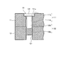
- FIG. 7 is a partial cross-sectional view showing a configuration of a fixing portion of two holder members by a cover screw.
- the cover screw 13 that fixes the holder members 11 and 12 to each other includes a screw head 131 having a thin disk shape and a screw portion 132.
- the threaded portion 132 has a distal end portion 132a provided with a screw thread, and a proximal end portion 132b that is positioned closer to the screw head 131 than the distal end portion 132a and has a cylindrical shape.
- the diameter of the proximal end portion 132b is smaller than the minimum outer diameter of the distal end portion 132a.
- the screw hole 111 has a placement portion 111a for placing the screw head 131 and a penetration portion 111b through which the screw portion 132 can be inserted and whose center axes coincide with each other.
- the mounting portion 111 a has a diameter larger than the diameter of the screw head 131 and is countersunk so that the depth from the opening is larger than the height of the screw head 131.
- a thread 111c is provided on a part of the inner peripheral surface of the insertion portion 111b, and can be screwed to the tip portion 132a.
- the screw hole 121 communicates with the screw hole 111 so that their center axes coincide with each other, and a screw thread that can be screwed with the tip end portion 132a is provided on the inner peripheral surface.
- the tip end portion 132 a is inserted into the screw hole 111 from the opening of the placement portion 111 a. After the tip portion 132a reaches the screw thread 111c by this insertion, the screw head 131 is rotated in a predetermined direction to screw the tip portion 132a to the screw thread 111c. If the screw head 131 is continuously rotated, the tip end portion 132a can reach the opening of the insertion portion 111b beyond the screw thread 111c. In this way, when the screw head 131 and the tip end portion 132a reach the opposite side via the thread 111c, the cover screw 13 is prevented from coming off the holder member 11.
- the screw head 131 is placed on the placement portion 111 a to align the holder member 12, and the tip end portion 132 a is screwed into the screw hole 121.
- the holder member 11 is sandwiched between the screw head 131 and the holder member 12, and the holder members 11 and 12 are fixed to each other.
- the cover screw 13 is screwed to the holder member 12 while being prevented from being detached from the holder member 11, the cover screw 13 is not dropped from the holder member 11 during assembly. . Therefore, the work can be performed without worrying about the top and bottom of the holder member 11 during assembly, and good workability can be obtained.
- the cover screw 13 has a problem that it has poor versatility and high manufacturing cost because the length of the base end portion 132b must be changed according to the plate thickness of the holder member 11.
- the present invention has been made in view of the above, and it is an object of the present invention to provide a probe holder and a probe unit that do not cause strength problems even when downsized, and that can keep the manufacturing cost low. .
- the probe holder according to the present invention is a conductive contact that is in contact with different circuit structures at both ends and inputs and outputs electrical signals between the different circuit structures.
- a probe holder that accommodates a plurality of probes according to a predetermined pattern, each of which has a plate shape and is laminated in the plate thickness direction, and the first and second holder members.
- a fixing screw fixed to each other, and a coil spring detachably attached to a screw portion of the fixing screw, wherein the first holder member is larger than a maximum outer diameter of the screw portion and is outside the coil spring.
- a first screw hole including an insertion portion through which the screw portion is inserted, wherein the second holder member has a large diameter portion having a diameter larger than an outer diameter of the coil spring; Diameter A second screw hole including a small-diameter portion provided with a screw thread capable of screwing the screw portion, the screw portion being screwed into the small-diameter portion, and the screw head of the fixing screw and the The first holder member is clamped by a second holder member.
- the probe holder according to the present invention is characterized in that, in the above invention, the maximum outer diameter of the thread portion is 2.0 mm or less.
- the probe holder according to the present invention is characterized in that, in the above invention, the number of turns of the coil spring is 2 or less.
- a probe unit according to the present invention includes the probe holder according to the present invention and a plurality of the contact probes accommodated in the probe holder.
- the fixing screw is prevented from coming off from one of the holder members by attaching the coil spring to the screw portion of the fixing screw that fixes the two holder members, a normal screw is applied as the fixing screw. be able to. Therefore, even if the diameter is reduced, there is no possibility of causing a strength problem, and the manufacturing cost can be kept low.
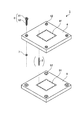
- FIG. 1 is a perspective view showing an overall configuration of a probe unit according to an embodiment of the present invention.
- FIG. 2 is an exploded perspective view showing the configuration of the probe unit according to the embodiment of the present invention.
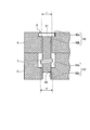
- FIG. 3 is a partial cross-sectional view showing a configuration of a fixing portion of the first and second holder members provided in the probe holder according to the embodiment of the present invention.
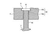
- FIG. 4 is a diagram illustrating a situation in which a coil spring is screwed into a fixing screw inserted through the first screw hole of the first holder member.
- FIG. 5 is a diagram illustrating a state in which the coil spring has been moved from the state illustrated in FIG. 4 to a predetermined position.
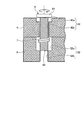
- FIG. 6 is a diagram illustrating a situation in which the fixing screw is screwed into the second holder member.
- FIG. 7 is a partial cross-sectional view showing a configuration of a fixing portion of two holder members in a conventional probe holder.
- FIG. 1 is a perspective view showing an overall configuration of a probe unit according to an embodiment of the present invention.
- FIG. 2 is an exploded perspective view showing the configuration of the probe unit according to the present embodiment.
- a probe unit 1 shown in FIGS. 1 and 2 is a device for inspecting electrical characteristics of a circuit structure such as a semiconductor integrated circuit, and an electrical signal between an inspection object and a circuit board each having two different circuit structures.
- a probe unit 1 shown in FIGS. 1 and 2 is a device for inspecting electrical characteristics of a circuit structure such as a semiconductor integrated circuit, and an electrical signal between an inspection object and a circuit board each having two different circuit structures.
- a probe holder 3 that accommodates and holds the plurality of contact probes 2 in a predetermined pattern. In FIG. 2, only one of the plurality of contact probes 2 is representatively described.
- the contact probe 2 is, for example, a both-end movable contact probe in which needle-like bodies are connected to both ends of a coil spring (see FIG. 11 of Patent Document 1). Note that the contact probe 2 is not limited to the movable type at both ends, and various types of conventionally known types can be applied.
- the probe holder 3 is formed using an insulating material such as a synthetic resin material having a high insulating property, and is laminated in the plate thickness direction, and a thin cylindrical screw head.
- 61 and a screw portion 62 each of which includes a plurality of metal fixing screws 6 for fixing the first holder member 4 and the second holder member 5 to each other and a wire such as a piano wire, and is attached to the screw portion 62.
- the maximum outer diameter of the screw portion 62 is 2.0 mm or less.
- the number of turns of the coil spring 7 is about two.
- the number of turns of the coil spring 7 is more preferably 2 or less. In FIG. 2, only one of the four fixing screws 6 is representatively described.
- the first holder member 4 has a plate shape.
- the first holder member 4 is penetrated in the plate thickness direction, and has a plurality of holding holes 41 through which a part of the contact probe 2 is inserted and held, and a plurality of first screw holes 42 through which the fixing screw 6 is inserted.
- the second holder member 5 has a plate shape like the first holder member 4.
- the second holder member 5 is penetrated in the thickness direction, and each of the second holder members 5 communicates with any one of the plurality of holding holes 41 so that their central axes coincide with each other, and a plurality of the contact probes 2 are inserted and held.
- Each of the holding holes 51 has a second screw hole 52 through which one of the plurality of first screw holes 42 and the center axis of each of the holding holes 51 communicate with each other and can be screwed into the fixing screw 6.
- the arrangement pattern of the holding holes 41 and 51 corresponds to the arrangement pattern of the electrodes to be inspected.
- FIG. 3 is a partial cross-sectional view showing a configuration of a fixed portion of the first holder member 4 and the second holder member 5.
- the first screw hole 42 includes a mounting portion 42 a for mounting the screw head 61, and an insertion portion 42 b for connecting the mounting portion 42 a with the central axis in communication and inserting the screw portion 62.
- the mounting portion 42 a has a diameter larger than the diameter of the screw head 61 and is countersunk so that the depth from the opening is larger than the height of the screw head 61.
- the insertion portion 42 b has a diameter r that is larger than the maximum outer diameter of the screw portion 62 and smaller than the outer diameter d of the coil spring 7. For this reason, the fixing screw 6 is prevented from being detached from the first holder member 4 by the coil spring 7.
- the second screw hole 52 is coaxial with the large-diameter portion 52a having a diameter larger than the outer diameter d of the coil spring 7, and has a smaller diameter than the large-diameter portion 52a, and is formed on the inner peripheral surface. And a small diameter portion 52b provided with a screw thread.
- the screw head 61 is placed on the placement portion 42a, and the screw portion 62 is screwed into the small diameter portion 52b.
- the coil spring 7 is screwed into the screw portion 62 and is located inside the large diameter portion 52a.
- the first holder member 4 is sandwiched between the screw head 61 and the second holder member 5 and fixed to the second holder member 5.
- the base material is either drilled, etched or stamped, or laser, electron beam Then, processing using any one of ion beam, wire discharge and the like is performed.
- the fixing screw 6 is inserted through the first screw hole 42. Specifically, the screw portion 62 is inserted from the opening of the placement portion 42a and inserted until the screw head 61 is placed on the placement portion 42a. Thereafter, as shown in FIG. 4, the coil spring 7 is screwed onto the screw portion 62 and attached. Since the coil spring 7 has only two windings, the coil spring 7 may be pushed in from the end of the screw part 62 so that the screw part 62 penetrates the hollow part of the coil spring 7.
- FIG. 5 is a view showing a state in which the coil spring 7 is moved to a predetermined position by screwing. Even if the first holder member 4 is turned upside down in the state shown in FIG. 5, the coil spring 7 is caught in the opening of the insertion portion 42 b, so that the fixing screw 6 does not fall off from the first holder member 4.
- the screw portion 62 is inserted into the second screw hole. 52b. Accordingly, the first holder member 4 is sandwiched between the screw head 61 and the second holder member 5 and fixed to the second holder member 5.
- the fixing screw 6 is obtained by screwing the coil spring 7 into the screw portion 62 of the fixing screw 6 that fixes the first holder member 4 and the second holder member 5 to each other. Is prevented from coming off from the first holder member 4, a normal screw can be applied as the fixing screw 6. Therefore, even if the maximum outer diameter of the threaded portion 62 is reduced to 2.0 mm or less, there is no possibility of causing a problem of strength unlike a cover screw. Further, since the fixing screw 6 is provided with a screw thread over the entire length of the screw portion 62, the fixing screw 6 is more versatile and easier to process than the cover screw. Accordingly, the manufacturing cost can be kept low.
- the above-described fixing structure (see FIG. 3) can be applied to other than the probe holder 3.
- the above-described fixing structure can be applied.
- the present invention can include various embodiments and the like not described herein, and various design changes and the like can be made without departing from the technical idea described in the claims. Can be applied.
- the present invention is useful for electrical inspection of electronic components such as semiconductor integrated circuits.
Landscapes
- Engineering & Computer Science (AREA)
- Computer Hardware Design (AREA)
- Microelectronics & Electronic Packaging (AREA)
- Physics & Mathematics (AREA)
- General Physics & Mathematics (AREA)
- Measuring Leads Or Probes (AREA)
Abstract
小型化しても強度的な問題を生じることがなく、製造コストも低く抑えることができるプローブホルダおよびプローブユニットを提供する。各々が板状をなし、板厚方向に積層された第1ホルダ部材および第2ホルダ部材と、第1ホルダ部材および第2ホルダ部材を相互に固定する固定ねじと、固定ねじのねじ部に着脱自在に装着されたコイルばねとを備え、第1ホルダ部材は、ねじ部の最大外径より大きくかつコイルばねの外径より小さい径を有し、ねじ部を挿通する挿通部を含む第1ねじ孔を備え、第2ホルダ部材は、コイルばねの外径より大きい径を有する大径部と、大径部に連通し、ねじ部を螺合可能なねじ山が設けられた小径部とを含む第2ねじ孔を備え、ねじ部を小径部に螺合し、固定ねじのねじ頭と第2ホルダ部材によって第1ホルダ部材を挟持する。
Description
本発明は、半導体集積回路等の電子部品の電気的な検査に用いる複数の導電性のコンタクトプローブを収容するプローブホルダおよび当該プローブホルダと複数のコンタクトプローブとを備えたプローブユニットに関する。
従来、半導体集積回路等の電子部品の導通状態検査や動作特性検査を行う際には、検査対象と該検査対象へ検査用信号を出力するテスターとの間の電気的な接続を図るため、複数の導電性のコンタクトプローブが用いられる。これらのコンタクトプローブは、検査対象の配線パターンに応じて配置され、プローブホルダに個別に収容される。プローブホルダは、コンタクトプローブを抜け止めする構成を有しており、板厚方向に重なった2枚の平板状のホルダ部材がねじによって相互に固定されている(例えば、特許文献1を参照)。
しかしながら、上述した特許文献1に記載の技術では、ねじを緩めた状態でねじがホルダ部材から脱落してしまうことがあるため、ホルダ部材の上下を意識しながら組立作業を行わなければならず、良好な作業性を得ることができなかった。この問題を解決するために、2枚のホルダ部材を相互に固定するねじとしてカバーねじ(例えば、特許文献2を参照)を用いることが考えられる。図7は、カバーねじによる2枚のホルダ部材の固定部分の構成を示す部分断面図である。図7において、ホルダ部材11、12を相互に固定するカバーねじ13は、薄い円盤状をなすねじ頭131と、ねじ部132とを備える。ねじ部132は、ねじ山が設けられている先端部132aと、先端部132aよりもねじ頭131の近くに位置し、円柱状をなす基端部132bとを有する。基端部132bの径は、先端部132aの最小外径より小さい。
次に、ホルダ部材11、12にそれぞれ設けられるカバーねじ13用のねじ孔111、121の構成を説明する。ねじ孔111は、ねじ頭131を載置する載置部111aと、ねじ部132を挿通可能であり、載置部111aと互いの中心軸が一致する挿通部111bとを有する。載置部111aは、ねじ頭131の径よりも大きい径を有するとともに、開口からの深さがねじ頭131の高さより大きくなるように座ぐりされている。挿通部111bの内周面の一部にはねじ山111cが設けられており、先端部132aと螺合可能である。一方、ねじ孔121は、ねじ孔111と互いの中心軸が一致して連通しており、内周面に先端部132aと螺合可能なねじ山が設けられている。
カバーねじ13を用いてホルダ部材11、12を相互に固定する際には、まず先端部132aを載置部111aの開口からねじ孔111へ挿入する。この挿入によって先端部132aがねじ山111cまで達した後、ねじ頭131を所定の方向に回転させて先端部132aをねじ山111cに螺合する。ねじ頭131を回転させ続けると、先端部132aはねじ山111cを越えて挿通部111bの開口に到達できるようになる。このようにしてねじ頭131と先端部132aがねじ山111cを介して反対側に位置する状態に達すると、カバーねじ13はホルダ部材11から抜け止めされる。その後、ねじ頭131を載置部111aに載置してホルダ部材12の位置合わせを行い、先端部132aをねじ孔121に螺合する。これにより、ホルダ部材11がねじ頭131とホルダ部材12によって挟持された状態となり、ホルダ部材11、12が相互に固定される。
以上説明したように、カバーねじ13は、ホルダ部材11に抜け止めされた状態でホルダ部材12に螺合されるため、組立の際にカバーねじ13がホルダ部材11から脱落してしまうことがない。したがって、組立の際にホルダ部材11の上下を気にすることなく作業を行うことができ、良好な作業性を得ることができる。
ところで近年、検査対象である電子部品の小型化に伴い、プローブホルダの小型化も求められてきている。プローブホルダを小型化する場合には、カバーねじ13の細径化が必要になってくる場合もある。しかしながら、例えばねじ部132の最大外径が2.0mm以下であるような微小なサイズのカバーねじ13を実現しようとすると、基端部132bの径をさらに細くしなければならないため、強度的な問題が生じるおそれがあった。
また、カバーねじ13は、ホルダ部材11の板厚に応じて基端部132bの長さを変更しなければならないため、汎用性に乏しく、製造コストがかかってしまうという問題があった。
本発明は、上記に鑑みてなされたものであって、小型化しても強度的な問題を生じることがなく、製造コストも低く抑えることができるプローブホルダおよびプローブユニットを提供することを目的とする。
上述した課題を解決し、目的を達成するために、本発明に係るプローブホルダは、両端部が異なる回路構造とそれぞれ接触し、前記異なる回路構造間の電気信号の入出力を行う導電性のコンタクトプローブを、所定のパターンにしたがって複数個収容するプローブホルダであって、各々が板状をなし、板厚方向に積層された第1および第2ホルダ部材と、前記第1および第2ホルダ部材を相互に固定する固定ねじと、前記固定ねじのねじ部に着脱自在に装着されたコイルばねと、を備え、前記第1ホルダ部材は、前記ねじ部の最大外径より大きくかつ前記コイルばねの外径より小さい径を有し、前記ねじ部を挿通する挿通部を含む第1ねじ孔を備え、前記第2ホルダ部材は、前記コイルばねの外径より大きい径を有する大径部と、前記大径部に連通し、前記ねじ部を螺合可能なねじ山が設けられた小径部とを含む第2ねじ孔を備え、前記ねじ部を前記小径部に螺合し、前記固定ねじのねじ頭と前記第2ホルダ部材によって前記第1ホルダ部材を挟持することを特徴とする。
また、本発明に係るプローブホルダは、上記発明において、前記ねじ部の最大外径は2.0mm以下であることを特徴とする。
また、本発明に係るプローブホルダは、上記発明において、前記コイルばねの巻き数は2以下であることを特徴とする。
また、本発明に係るプローブユニットは、上記発明に係るプローブホルダと、前記プローブホルダが収容する複数の前記コンタクトプローブと、を備えたことを特徴とする。
本発明によれば、二つのホルダ部材を固定する固定ねじのねじ部にコイルばねを装着することによって固定ねじを一方のホルダ部材から抜け止めしているため、固定ねじとして通常のねじを適用することができる。したがって、細径化しても強度的な問題を生じるおそれがなく、製造コストも低く抑えることが可能となる。
以下、添付図面を参照して本発明を実施するための形態を説明する。なお、図面は模式的なものであって、各部分の厚みと幅との関係、それぞれの部分の厚みの比率などは現実のものとは異なる場合もあることに留意すべきであり、図面の相互間においても互いの寸法の関係や比率が異なる部分が含まれる場合があることは勿論である。
図1は、本発明の一実施の形態に係るプローブユニットの全体構成を示す斜視図である。また、図2は、本実施の形態に係るプローブユニットの構成を示す分解斜視図である。図1および図2に示すプローブユニット1は、半導体集積回路等の回路構造の電気的特性を検査する装置であり、異なる二つの回路構造をそれぞれ具備した検査対象と回路基板との間で電気信号の送受信を行う複数の導電性のコンタクトプローブ2と、複数のコンタクトプローブ2を所定のパターンで収容して保持するプローブホルダ3とを備える。なお、図2では、複数のコンタクトプローブ2のうち1本のみを代表的に記載している。
コンタクトプローブ2は、例えばコイルばねの両端部に針状体を連結した両端可動型のコンタクトプローブである(上記特許文献1の図11を参照)。なお、コンタクトプローブ2は両端可動型に限られるわけではなく、従来知られている様々なタイプのものを適用することが可能である。
プローブホルダ3は、絶縁性が高い合成樹脂材などの絶縁性材料を用いてそれぞれ形成され、板厚方向に積層された第1ホルダ部材4および第2ホルダ部材5と、薄い円柱状のねじ頭61およびねじ部62を有し、第1ホルダ部材4と第2ホルダ部材5とを相互に固定する複数の金属製の固定ねじ6と、ピアノ線等の線材からなり、ねじ部62に装着されるコイルばね7と、を備える。ねじ部62の最大外径は2.0mm以下である。また、コイルばね7の巻き数は2巻き程度である。コイルばね7の巻き数は、2以下であればより好ましい。なお、図2では、4つの固定ねじ6のうち1本のみを代表的に記載している。
第1ホルダ部材4は板状をなしている。第1ホルダ部材4は、その板厚方向に貫通され、コンタクトプローブ2の一部を挿通して保持する複数の保持孔41と、固定ねじ6を挿通する複数の第1ねじ孔42とを有する。一方、第2ホルダ部材5は、第1ホルダ部材4と同様に板状をなしている。第2ホルダ部材5は、その板厚方向に貫通され、各々が複数の保持孔41のいずれかと互いの中心軸が一致して連通し、コンタクトプローブ2の一部を挿通して保持する複数の保持孔51と、各々が複数の第1ねじ孔42のいずれかと互いの中心軸が一致して連通し、固定ねじ6を螺合可能な第2ねじ孔52とを有する。保持孔41、51の配置パターンは、検査対象の電極の配置パターンに対応している。
なお、第1ホルダ部材4および第2ホルダ部材5として、金属等の導電性材料からなる母材の表面に絶縁被膜を形成したものを適用することも可能である。
図3は、第1ホルダ部材4と第2ホルダ部材5の固定部分の構成を示す部分断面図である。まず、第1ねじ孔42、第2ねじ孔52の構成を説明する。第1ねじ孔42は、ねじ頭61を載置する載置部42aと、載置部42aと中心軸が一致して連通し、ねじ部62を挿通する挿通部42bとを備える。載置部42aは、ねじ頭61の径よりも大きい径を有するとともに、開口からの深さがねじ頭61の高さよりも大きくなるように座ぐりされている。挿通部42bは、ねじ部62の最大外径よりも大きく、かつコイルばね7の外径dよりも小さい径rを有する。このため、固定ねじ6はコイルばね7によって第1ホルダ部材4から抜け止めされる。
第2ねじ孔52は、コイルばね7の外径dより大きい径を有する大径部52aと、大径部52aと同軸をなし、大径部52aより小さい径を有し、かつ内周面にねじ山が設けられた小径部52bとを有する。
図3において、ねじ頭61は載置部42aに載置され、ねじ部62は小径部52bに螺合されている。また、コイルばね7はねじ部62に螺合され、大径部52aの内部に位置している。この状態で、第1ホルダ部材4はねじ頭61および第2ホルダ部材5によって挟持され、第2ホルダ部材5に固定されている。
保持孔41、51、および第1ねじ孔42、第2ねじ孔52を形成する際には、母材に対してドリル加工、エッチング、打抜成形のいずれかを行うか、あるいはレーザ、電子ビーム、イオンビーム、ワイヤ放電などのいずれかを用いた加工を施す。
次に、固定ねじ6による第1ホルダ部材4と第2ホルダ部材5の固定方法を、図4~図6を参照して説明する。まず、固定ねじ6を第1ねじ孔42に挿通する。具体的には、ねじ部62を載置部42aの開口から挿入し、ねじ頭61が載置部42aに載置された状態となるまで挿入する。その後、図4に示すように、コイルばね7をねじ部62に螺合して装着する。なお、コイルばね7は巻き数が2と少ないため、ねじ部62がコイルばね7の中空部を貫通するようにコイルばね7をねじ部62の端部から押し込んで装着するようにしてもよい。
コイルばね7を螺合し続けると、コイルばね7は徐々にねじ頭61の方へ近づいていく。図5は、螺合によってコイルばね7を所定の位置まで移動させた状態を示す図である。図5に示す状態で第1ホルダ部材4の上下を逆にしても、コイルばね7が挿通部42bの開口に引っ掛かるため、固定ねじ6が第1ホルダ部材4から脱落してしまうことはない。
続いて、複数のコンタクトプローブ2を第2ホルダ部材5に挿通し、第1ホルダ部材4と第2ホルダ部材5の位置決めを行った後(図6を参照)、ねじ部62を第2ねじ孔52bに螺合する。これにより、第1ホルダ部材4はねじ頭61および第2ホルダ部材5によって挟持され、第2ホルダ部材5に固定される。
以上説明した本発明の一実施の形態によれば、第1ホルダ部材4と第2ホルダ部材5を相互に固定する固定ねじ6のねじ部62にコイルばね7を螺合することによって固定ねじ6を第1ホルダ部材4から抜け止めしているため、固定ねじ6として通常のねじを適用することができる。したがって、ねじ部62の最大外径を2.0mm以下まで細径化してもカバーねじのように強度的な問題を生じるおそれがない。また、固定ねじ6はねじ部62の全長にわたってねじ山が設けられているため、カバーねじよりも汎用性が高く加工も容易である。したがって、製造コストも低く抑えることが可能となる。
なお、上述した固定構造(図3を参照)は、プローブホルダ3以外にも適用することができる。例えば、プローブユニット1を回路基板に固定する場合にも上述した固定構造を適用することができる。
このように、本発明は、ここでは説明していない様々な実施の形態等を含みうるものであり、特許請求の範囲に記載された技術的思想を逸脱しない範囲内において、種々の設計変更等を施すことが可能である。
本発明は、半導体集積回路等の電子部品の電気的な検査を行うのに有用である。
1 プローブユニット
2 コンタクトプローブ
3 プローブホルダ
4 第1ホルダ部材
5 第2ホルダ部材
6 固定ねじ
7 コイルばね
11、12 ホルダ部材
13 カバーねじ
41、51 保持孔
42 第1ねじ孔
42a、111a 載置部
42b、111b 挿通部
52 第2ねじ孔
52a 大径部
52b 小径部
61、131 ねじ頭
62、132 ねじ部
111、121 ねじ孔
111c ねじ山
132a 先端部
132b 基端部
2 コンタクトプローブ
3 プローブホルダ
4 第1ホルダ部材
5 第2ホルダ部材
6 固定ねじ
7 コイルばね
11、12 ホルダ部材
13 カバーねじ
41、51 保持孔
42 第1ねじ孔
42a、111a 載置部
42b、111b 挿通部
52 第2ねじ孔
52a 大径部
52b 小径部
61、131 ねじ頭
62、132 ねじ部
111、121 ねじ孔
111c ねじ山
132a 先端部
132b 基端部
Claims (4)
- 両端部が異なる回路構造とそれぞれ接触し、前記異なる回路構造間の電気信号の入出力を行う導電性のコンタクトプローブを、所定のパターンにしたがって複数個収容するプローブホルダであって、
各々が板状をなし、板厚方向に積層された第1および第2ホルダ部材と、
前記第1および第2ホルダ部材を相互に固定する固定ねじと、
前記固定ねじのねじ部に着脱自在に装着されたコイルばねと、
を備え、
前記第1ホルダ部材は、
前記ねじ部の最大外径より大きくかつ前記コイルばねの外径より小さい径を有し、前記ねじ部を挿通する挿通部を含む第1ねじ孔を備え、
前記第2ホルダ部材は、
前記コイルばねの外径より大きい径を有する大径部と、前記大径部に連通し、前記ねじ部を螺合可能なねじ山が設けられた小径部とを含む第2ねじ孔を備え、
前記ねじ部を前記小径部に螺合し、前記固定ねじのねじ頭と前記第2ホルダ部材によって前記第1ホルダ部材を挟持することを特徴とするプローブホルダ。 - 前記ねじ部の最大外径は2.0mm以下であることを特徴とする請求項1記載のプローブホルダ。
- 前記コイルばねの巻き数は2以下であることを特徴とする請求項1または2記載のプローブホルダ。
- 請求項1~3のいずれか一項記載のプローブホルダと、
前記プローブホルダが収容する複数の前記コンタクトプローブと、
を備えたことを特徴とするプローブユニット。
Priority Applications (1)
| Application Number | Priority Date | Filing Date | Title |
|---|---|---|---|
| JP2011508406A JPWO2010117080A1 (ja) | 2009-04-10 | 2010-04-12 | プローブホルダおよびプローブユニット |
Applications Claiming Priority (2)
| Application Number | Priority Date | Filing Date | Title |
|---|---|---|---|
| JP2009096237 | 2009-04-10 | ||
| JP2009-096237 | 2009-04-10 |
Publications (1)
| Publication Number | Publication Date |
|---|---|
| WO2010117080A1 true WO2010117080A1 (ja) | 2010-10-14 |
Family
ID=42936363
Family Applications (1)
| Application Number | Title | Priority Date | Filing Date |
|---|---|---|---|
| PCT/JP2010/056539 Ceased WO2010117080A1 (ja) | 2009-04-10 | 2010-04-12 | プローブホルダおよびプローブユニット |
Country Status (2)
| Country | Link |
|---|---|
| JP (1) | JPWO2010117080A1 (ja) |
| WO (1) | WO2010117080A1 (ja) |
Cited By (4)
| Publication number | Priority date | Publication date | Assignee | Title |
|---|---|---|---|---|
| JP2018185302A (ja) * | 2017-04-21 | 2018-11-22 | Contact Standard株式会社 | コンタクトピン及び電子機器 |
| EP3647740A1 (en) * | 2018-11-02 | 2020-05-06 | Yokogawa Electric Corporation | Module connection structure and measuring instrument |
| JPWO2021182193A1 (ja) * | 2020-03-11 | 2021-09-16 | ||
| WO2022158032A1 (ja) * | 2021-01-19 | 2022-07-28 | 日本発條株式会社 | プローブユニット |
Citations (4)
| Publication number | Priority date | Publication date | Assignee | Title |
|---|---|---|---|---|
| JPS5112853U (ja) * | 1974-07-15 | 1976-01-30 | ||
| JPS5580514U (ja) * | 1978-11-29 | 1980-06-03 | ||
| JPH09273532A (ja) * | 1996-04-05 | 1997-10-21 | Nitsuko Corp | 筐体のカバー取付装置 |
| JP2002139513A (ja) * | 2000-11-02 | 2002-05-17 | Nhk Spring Co Ltd | コンタクトプローブユニット |
Family Cites Families (1)
| Publication number | Priority date | Publication date | Assignee | Title |
|---|---|---|---|---|
| JPS6369809U (ja) * | 1986-10-27 | 1988-05-11 |
-
2010
- 2010-04-12 WO PCT/JP2010/056539 patent/WO2010117080A1/ja not_active Ceased
- 2010-04-12 JP JP2011508406A patent/JPWO2010117080A1/ja active Pending
Patent Citations (4)
| Publication number | Priority date | Publication date | Assignee | Title |
|---|---|---|---|---|
| JPS5112853U (ja) * | 1974-07-15 | 1976-01-30 | ||
| JPS5580514U (ja) * | 1978-11-29 | 1980-06-03 | ||
| JPH09273532A (ja) * | 1996-04-05 | 1997-10-21 | Nitsuko Corp | 筐体のカバー取付装置 |
| JP2002139513A (ja) * | 2000-11-02 | 2002-05-17 | Nhk Spring Co Ltd | コンタクトプローブユニット |
Cited By (12)
| Publication number | Priority date | Publication date | Assignee | Title |
|---|---|---|---|---|
| JP2018185302A (ja) * | 2017-04-21 | 2018-11-22 | Contact Standard株式会社 | コンタクトピン及び電子機器 |
| EP3647740A1 (en) * | 2018-11-02 | 2020-05-06 | Yokogawa Electric Corporation | Module connection structure and measuring instrument |
| US11031963B2 (en) | 2018-11-02 | 2021-06-08 | Yokogawa Electric Corporation | Module connection structure and measuring instrument |
| JPWO2021182193A1 (ja) * | 2020-03-11 | 2021-09-16 | ||
| CN115244408A (zh) * | 2020-03-11 | 2022-10-25 | 日本发条株式会社 | 探针卡 |
| JP7682152B2 (ja) | 2020-03-11 | 2025-05-23 | 日本発條株式会社 | プローブカード |
| WO2022158032A1 (ja) * | 2021-01-19 | 2022-07-28 | 日本発條株式会社 | プローブユニット |
| JPWO2022158032A1 (ja) * | 2021-01-19 | 2022-07-28 | ||
| KR20230118646A (ko) * | 2021-01-19 | 2023-08-11 | 닛폰 하츠죠 가부시키가이샤 | 프로브 유닛 |
| JP7650901B2 (ja) | 2021-01-19 | 2025-03-25 | 日本発條株式会社 | プローブユニット |
| KR102859538B1 (ko) | 2021-01-19 | 2025-09-12 | 닛폰 하츠죠 가부시키가이샤 | 프로브 유닛 |
| US12498396B2 (en) | 2021-01-19 | 2025-12-16 | Nhk Spring Co., Ltd. | Probe unit |
Also Published As
| Publication number | Publication date |
|---|---|
| JPWO2010117080A1 (ja) | 2012-10-18 |
Similar Documents
| Publication | Publication Date | Title |
|---|---|---|
| JP5607934B2 (ja) | プローブユニット | |
| TWI717915B (zh) | 探針單元 | |
| JP5776687B2 (ja) | 検査用接触子及び検査用治具 | |
| JP2004325305A (ja) | Icソケット | |
| JP2004325306A (ja) | 検査用同軸プローブおよびそれを用いた検査ユニット | |
| KR101979060B1 (ko) | 프로브 유닛, 기판 검사 장치 및 프로브 유닛 제조 방법 | |
| TWI722680B (zh) | 探針單元 | |
| JP2010276510A (ja) | 検査用治具 | |
| KR101157879B1 (ko) | 검사용 치구 및 접촉자 | |
| JP6367249B2 (ja) | プローブユニット | |
| WO2018209901A1 (zh) | 垂直探针卡 | |
| WO2017138305A1 (ja) | 接触端子、検査治具、及び検査装置 | |
| JP2017054773A (ja) | 接続治具、基板検査装置、及び接続治具の製造方法 | |
| WO2010117080A1 (ja) | プローブホルダおよびプローブユニット | |
| WO2021193304A1 (ja) | プローブユニット | |
| TW201840984A (zh) | 探針固持具及探針單元 | |
| JP2009192419A (ja) | プローブユニット及び検査装置 | |
| KR20100052520A (ko) | 전기접속구조, 단자장치, 소켓, 전자부품시험장치 및 소켓의 제조방법 | |
| JP2010078432A (ja) | 基板検査治具及び接触子 | |
| JP3154264U (ja) | プローブピン及び基板検査用プローブユニット | |
| WO2014123235A1 (ja) | プローブユニット用ベース部材、プローブホルダ、プローブユニット、プローブユニット用ベース部材の製造方法およびプローブユニット用積層構造体 | |
| WO2011162363A1 (ja) | プローブホルダ、プローブホルダおよびプローブユニットの製造方法 | |
| JPWO2012067125A1 (ja) | プローブユニット | |
| CN206848311U (zh) | 检查夹具及具备该检查夹具的检查装置 | |
| WO2020045066A1 (ja) | プローブピン用ハウジング、検査治具、検査ユニットおよび検査装置 |
Legal Events
| Date | Code | Title | Description |
|---|---|---|---|
| 121 | Ep: the epo has been informed by wipo that ep was designated in this application |
Ref document number: 10761778 Country of ref document: EP Kind code of ref document: A1 |
|
| WWE | Wipo information: entry into national phase |
Ref document number: 2011508406 Country of ref document: JP |
|
| NENP | Non-entry into the national phase |
Ref country code: DE |
|
| 122 | Ep: pct application non-entry in european phase |
Ref document number: 10761778 Country of ref document: EP Kind code of ref document: A1 |