WO2010110201A1 - 誘電体磁器組成物、多層誘電体基板、電子部品、及び誘電体磁器組成物の製造方法 - Google Patents
誘電体磁器組成物、多層誘電体基板、電子部品、及び誘電体磁器組成物の製造方法 Download PDFInfo
- Publication number
- WO2010110201A1 WO2010110201A1 PCT/JP2010/054792 JP2010054792W WO2010110201A1 WO 2010110201 A1 WO2010110201 A1 WO 2010110201A1 JP 2010054792 W JP2010054792 W JP 2010054792W WO 2010110201 A1 WO2010110201 A1 WO 2010110201A1
- Authority
- WO
- WIPO (PCT)
- Prior art keywords
- weight
- terms
- dielectric
- ceramic composition
- dielectric ceramic
- Prior art date
- Legal status (The legal status is an assumption and is not a legal conclusion. Google has not performed a legal analysis and makes no representation as to the accuracy of the status listed.)
- Ceased
Links
Images






Classifications
-
- C—CHEMISTRY; METALLURGY
- C04—CEMENTS; CONCRETE; ARTIFICIAL STONE; CERAMICS; REFRACTORIES
- C04B—LIME, MAGNESIA; SLAG; CEMENTS; COMPOSITIONS THEREOF, e.g. MORTARS, CONCRETE OR LIKE BUILDING MATERIALS; ARTIFICIAL STONE; CERAMICS; REFRACTORIES; TREATMENT OF NATURAL STONE
- C04B35/00—Shaped ceramic products characterised by their composition; Ceramics compositions; Processing powders of inorganic compounds preparatory to the manufacturing of ceramic products
- C04B35/01—Shaped ceramic products characterised by their composition; Ceramics compositions; Processing powders of inorganic compounds preparatory to the manufacturing of ceramic products based on oxide ceramics
- C04B35/46—Shaped ceramic products characterised by their composition; Ceramics compositions; Processing powders of inorganic compounds preparatory to the manufacturing of ceramic products based on oxide ceramics based on titanium oxides or titanates
- C04B35/462—Shaped ceramic products characterised by their composition; Ceramics compositions; Processing powders of inorganic compounds preparatory to the manufacturing of ceramic products based on oxide ceramics based on titanium oxides or titanates based on titanates
- C04B35/465—Shaped ceramic products characterised by their composition; Ceramics compositions; Processing powders of inorganic compounds preparatory to the manufacturing of ceramic products based on oxide ceramics based on titanium oxides or titanates based on titanates based on alkaline earth metal titanates
- C04B35/47—Shaped ceramic products characterised by their composition; Ceramics compositions; Processing powders of inorganic compounds preparatory to the manufacturing of ceramic products based on oxide ceramics based on titanium oxides or titanates based on titanates based on alkaline earth metal titanates based on strontium titanates
-
- B—PERFORMING OPERATIONS; TRANSPORTING
- B32—LAYERED PRODUCTS
- B32B—LAYERED PRODUCTS, i.e. PRODUCTS BUILT-UP OF STRATA OF FLAT OR NON-FLAT, e.g. CELLULAR OR HONEYCOMB, FORM
- B32B18/00—Layered products essentially comprising ceramics, e.g. refractory products
-
- C—CHEMISTRY; METALLURGY
- C04—CEMENTS; CONCRETE; ARTIFICIAL STONE; CERAMICS; REFRACTORIES
- C04B—LIME, MAGNESIA; SLAG; CEMENTS; COMPOSITIONS THEREOF, e.g. MORTARS, CONCRETE OR LIKE BUILDING MATERIALS; ARTIFICIAL STONE; CERAMICS; REFRACTORIES; TREATMENT OF NATURAL STONE
- C04B35/00—Shaped ceramic products characterised by their composition; Ceramics compositions; Processing powders of inorganic compounds preparatory to the manufacturing of ceramic products
- C04B35/01—Shaped ceramic products characterised by their composition; Ceramics compositions; Processing powders of inorganic compounds preparatory to the manufacturing of ceramic products based on oxide ceramics
- C04B35/16—Shaped ceramic products characterised by their composition; Ceramics compositions; Processing powders of inorganic compounds preparatory to the manufacturing of ceramic products based on oxide ceramics based on silicates other than clay
- C04B35/18—Shaped ceramic products characterised by their composition; Ceramics compositions; Processing powders of inorganic compounds preparatory to the manufacturing of ceramic products based on oxide ceramics based on silicates other than clay rich in aluminium oxide
-
- C—CHEMISTRY; METALLURGY
- C04—CEMENTS; CONCRETE; ARTIFICIAL STONE; CERAMICS; REFRACTORIES
- C04B—LIME, MAGNESIA; SLAG; CEMENTS; COMPOSITIONS THEREOF, e.g. MORTARS, CONCRETE OR LIKE BUILDING MATERIALS; ARTIFICIAL STONE; CERAMICS; REFRACTORIES; TREATMENT OF NATURAL STONE
- C04B35/00—Shaped ceramic products characterised by their composition; Ceramics compositions; Processing powders of inorganic compounds preparatory to the manufacturing of ceramic products
- C04B35/01—Shaped ceramic products characterised by their composition; Ceramics compositions; Processing powders of inorganic compounds preparatory to the manufacturing of ceramic products based on oxide ceramics
- C04B35/16—Shaped ceramic products characterised by their composition; Ceramics compositions; Processing powders of inorganic compounds preparatory to the manufacturing of ceramic products based on oxide ceramics based on silicates other than clay
- C04B35/18—Shaped ceramic products characterised by their composition; Ceramics compositions; Processing powders of inorganic compounds preparatory to the manufacturing of ceramic products based on oxide ceramics based on silicates other than clay rich in aluminium oxide
- C04B35/195—Alkaline earth aluminosilicates, e.g. cordierite or anorthite
-
- C—CHEMISTRY; METALLURGY
- C04—CEMENTS; CONCRETE; ARTIFICIAL STONE; CERAMICS; REFRACTORIES
- C04B—LIME, MAGNESIA; SLAG; CEMENTS; COMPOSITIONS THEREOF, e.g. MORTARS, CONCRETE OR LIKE BUILDING MATERIALS; ARTIFICIAL STONE; CERAMICS; REFRACTORIES; TREATMENT OF NATURAL STONE
- C04B35/00—Shaped ceramic products characterised by their composition; Ceramics compositions; Processing powders of inorganic compounds preparatory to the manufacturing of ceramic products
- C04B35/01—Shaped ceramic products characterised by their composition; Ceramics compositions; Processing powders of inorganic compounds preparatory to the manufacturing of ceramic products based on oxide ceramics
- C04B35/46—Shaped ceramic products characterised by their composition; Ceramics compositions; Processing powders of inorganic compounds preparatory to the manufacturing of ceramic products based on oxide ceramics based on titanium oxides or titanates
- C04B35/462—Shaped ceramic products characterised by their composition; Ceramics compositions; Processing powders of inorganic compounds preparatory to the manufacturing of ceramic products based on oxide ceramics based on titanium oxides or titanates based on titanates
-
- C—CHEMISTRY; METALLURGY
- C04—CEMENTS; CONCRETE; ARTIFICIAL STONE; CERAMICS; REFRACTORIES
- C04B—LIME, MAGNESIA; SLAG; CEMENTS; COMPOSITIONS THEREOF, e.g. MORTARS, CONCRETE OR LIKE BUILDING MATERIALS; ARTIFICIAL STONE; CERAMICS; REFRACTORIES; TREATMENT OF NATURAL STONE
- C04B35/00—Shaped ceramic products characterised by their composition; Ceramics compositions; Processing powders of inorganic compounds preparatory to the manufacturing of ceramic products
- C04B35/01—Shaped ceramic products characterised by their composition; Ceramics compositions; Processing powders of inorganic compounds preparatory to the manufacturing of ceramic products based on oxide ceramics
- C04B35/46—Shaped ceramic products characterised by their composition; Ceramics compositions; Processing powders of inorganic compounds preparatory to the manufacturing of ceramic products based on oxide ceramics based on titanium oxides or titanates
- C04B35/462—Shaped ceramic products characterised by their composition; Ceramics compositions; Processing powders of inorganic compounds preparatory to the manufacturing of ceramic products based on oxide ceramics based on titanium oxides or titanates based on titanates
- C04B35/465—Shaped ceramic products characterised by their composition; Ceramics compositions; Processing powders of inorganic compounds preparatory to the manufacturing of ceramic products based on oxide ceramics based on titanium oxides or titanates based on titanates based on alkaline earth metal titanates
-
- C—CHEMISTRY; METALLURGY
- C04—CEMENTS; CONCRETE; ARTIFICIAL STONE; CERAMICS; REFRACTORIES
- C04B—LIME, MAGNESIA; SLAG; CEMENTS; COMPOSITIONS THEREOF, e.g. MORTARS, CONCRETE OR LIKE BUILDING MATERIALS; ARTIFICIAL STONE; CERAMICS; REFRACTORIES; TREATMENT OF NATURAL STONE
- C04B35/00—Shaped ceramic products characterised by their composition; Ceramics compositions; Processing powders of inorganic compounds preparatory to the manufacturing of ceramic products
- C04B35/622—Forming processes; Processing powders of inorganic compounds preparatory to the manufacturing of ceramic products
- C04B35/626—Preparing or treating the powders individually or as batches ; preparing or treating macroscopic reinforcing agents for ceramic products, e.g. fibres; mechanical aspects section B
- C04B35/62605—Treating the starting powders individually or as mixtures
- C04B35/62685—Treating the starting powders individually or as mixtures characterised by the order of addition of constituents or additives
-
- H—ELECTRICITY
- H01—ELECTRIC ELEMENTS
- H01B—CABLES; CONDUCTORS; INSULATORS; SELECTION OF MATERIALS FOR THEIR CONDUCTIVE, INSULATING OR DIELECTRIC PROPERTIES
- H01B3/00—Insulators or insulating bodies characterised by the insulating materials; Selection of materials for their insulating or dielectric properties
- H01B3/02—Insulators or insulating bodies characterised by the insulating materials; Selection of materials for their insulating or dielectric properties mainly consisting of inorganic substances
- H01B3/12—Insulators or insulating bodies characterised by the insulating materials; Selection of materials for their insulating or dielectric properties mainly consisting of inorganic substances ceramics
-
- C—CHEMISTRY; METALLURGY
- C04—CEMENTS; CONCRETE; ARTIFICIAL STONE; CERAMICS; REFRACTORIES
- C04B—LIME, MAGNESIA; SLAG; CEMENTS; COMPOSITIONS THEREOF, e.g. MORTARS, CONCRETE OR LIKE BUILDING MATERIALS; ARTIFICIAL STONE; CERAMICS; REFRACTORIES; TREATMENT OF NATURAL STONE
- C04B2235/00—Aspects relating to ceramic starting mixtures or sintered ceramic products
- C04B2235/02—Composition of constituents of the starting material or of secondary phases of the final product
- C04B2235/30—Constituents and secondary phases not being of a fibrous nature
- C04B2235/32—Metal oxides, mixed metal oxides, or oxide-forming salts thereof, e.g. carbonates, nitrates, (oxy)hydroxides, chlorides
- C04B2235/3201—Alkali metal oxides or oxide-forming salts thereof
-
- C—CHEMISTRY; METALLURGY
- C04—CEMENTS; CONCRETE; ARTIFICIAL STONE; CERAMICS; REFRACTORIES
- C04B—LIME, MAGNESIA; SLAG; CEMENTS; COMPOSITIONS THEREOF, e.g. MORTARS, CONCRETE OR LIKE BUILDING MATERIALS; ARTIFICIAL STONE; CERAMICS; REFRACTORIES; TREATMENT OF NATURAL STONE
- C04B2235/00—Aspects relating to ceramic starting mixtures or sintered ceramic products
- C04B2235/02—Composition of constituents of the starting material or of secondary phases of the final product
- C04B2235/30—Constituents and secondary phases not being of a fibrous nature
- C04B2235/32—Metal oxides, mixed metal oxides, or oxide-forming salts thereof, e.g. carbonates, nitrates, (oxy)hydroxides, chlorides
- C04B2235/3205—Alkaline earth oxides or oxide forming salts thereof, e.g. beryllium oxide
- C04B2235/3206—Magnesium oxides or oxide-forming salts thereof
-
- C—CHEMISTRY; METALLURGY
- C04—CEMENTS; CONCRETE; ARTIFICIAL STONE; CERAMICS; REFRACTORIES
- C04B—LIME, MAGNESIA; SLAG; CEMENTS; COMPOSITIONS THEREOF, e.g. MORTARS, CONCRETE OR LIKE BUILDING MATERIALS; ARTIFICIAL STONE; CERAMICS; REFRACTORIES; TREATMENT OF NATURAL STONE
- C04B2235/00—Aspects relating to ceramic starting mixtures or sintered ceramic products
- C04B2235/02—Composition of constituents of the starting material or of secondary phases of the final product
- C04B2235/30—Constituents and secondary phases not being of a fibrous nature
- C04B2235/32—Metal oxides, mixed metal oxides, or oxide-forming salts thereof, e.g. carbonates, nitrates, (oxy)hydroxides, chlorides
- C04B2235/3205—Alkaline earth oxides or oxide forming salts thereof, e.g. beryllium oxide
- C04B2235/3208—Calcium oxide or oxide-forming salts thereof, e.g. lime
-
- C—CHEMISTRY; METALLURGY
- C04—CEMENTS; CONCRETE; ARTIFICIAL STONE; CERAMICS; REFRACTORIES
- C04B—LIME, MAGNESIA; SLAG; CEMENTS; COMPOSITIONS THEREOF, e.g. MORTARS, CONCRETE OR LIKE BUILDING MATERIALS; ARTIFICIAL STONE; CERAMICS; REFRACTORIES; TREATMENT OF NATURAL STONE
- C04B2235/00—Aspects relating to ceramic starting mixtures or sintered ceramic products
- C04B2235/02—Composition of constituents of the starting material or of secondary phases of the final product
- C04B2235/30—Constituents and secondary phases not being of a fibrous nature
- C04B2235/32—Metal oxides, mixed metal oxides, or oxide-forming salts thereof, e.g. carbonates, nitrates, (oxy)hydroxides, chlorides
- C04B2235/3205—Alkaline earth oxides or oxide forming salts thereof, e.g. beryllium oxide
- C04B2235/3213—Strontium oxides or oxide-forming salts thereof
-
- C—CHEMISTRY; METALLURGY
- C04—CEMENTS; CONCRETE; ARTIFICIAL STONE; CERAMICS; REFRACTORIES
- C04B—LIME, MAGNESIA; SLAG; CEMENTS; COMPOSITIONS THEREOF, e.g. MORTARS, CONCRETE OR LIKE BUILDING MATERIALS; ARTIFICIAL STONE; CERAMICS; REFRACTORIES; TREATMENT OF NATURAL STONE
- C04B2235/00—Aspects relating to ceramic starting mixtures or sintered ceramic products
- C04B2235/02—Composition of constituents of the starting material or of secondary phases of the final product
- C04B2235/30—Constituents and secondary phases not being of a fibrous nature
- C04B2235/32—Metal oxides, mixed metal oxides, or oxide-forming salts thereof, e.g. carbonates, nitrates, (oxy)hydroxides, chlorides
- C04B2235/3217—Aluminum oxide or oxide forming salts thereof, e.g. bauxite, alpha-alumina
-
- C—CHEMISTRY; METALLURGY
- C04—CEMENTS; CONCRETE; ARTIFICIAL STONE; CERAMICS; REFRACTORIES
- C04B—LIME, MAGNESIA; SLAG; CEMENTS; COMPOSITIONS THEREOF, e.g. MORTARS, CONCRETE OR LIKE BUILDING MATERIALS; ARTIFICIAL STONE; CERAMICS; REFRACTORIES; TREATMENT OF NATURAL STONE
- C04B2235/00—Aspects relating to ceramic starting mixtures or sintered ceramic products
- C04B2235/02—Composition of constituents of the starting material or of secondary phases of the final product
- C04B2235/30—Constituents and secondary phases not being of a fibrous nature
- C04B2235/32—Metal oxides, mixed metal oxides, or oxide-forming salts thereof, e.g. carbonates, nitrates, (oxy)hydroxides, chlorides
- C04B2235/3224—Rare earth oxide or oxide forming salts thereof, e.g. scandium oxide
-
- C—CHEMISTRY; METALLURGY
- C04—CEMENTS; CONCRETE; ARTIFICIAL STONE; CERAMICS; REFRACTORIES
- C04B—LIME, MAGNESIA; SLAG; CEMENTS; COMPOSITIONS THEREOF, e.g. MORTARS, CONCRETE OR LIKE BUILDING MATERIALS; ARTIFICIAL STONE; CERAMICS; REFRACTORIES; TREATMENT OF NATURAL STONE
- C04B2235/00—Aspects relating to ceramic starting mixtures or sintered ceramic products
- C04B2235/02—Composition of constituents of the starting material or of secondary phases of the final product
- C04B2235/30—Constituents and secondary phases not being of a fibrous nature
- C04B2235/32—Metal oxides, mixed metal oxides, or oxide-forming salts thereof, e.g. carbonates, nitrates, (oxy)hydroxides, chlorides
- C04B2235/3224—Rare earth oxide or oxide forming salts thereof, e.g. scandium oxide
- C04B2235/3227—Lanthanum oxide or oxide-forming salts thereof
-
- C—CHEMISTRY; METALLURGY
- C04—CEMENTS; CONCRETE; ARTIFICIAL STONE; CERAMICS; REFRACTORIES
- C04B—LIME, MAGNESIA; SLAG; CEMENTS; COMPOSITIONS THEREOF, e.g. MORTARS, CONCRETE OR LIKE BUILDING MATERIALS; ARTIFICIAL STONE; CERAMICS; REFRACTORIES; TREATMENT OF NATURAL STONE
- C04B2235/00—Aspects relating to ceramic starting mixtures or sintered ceramic products
- C04B2235/02—Composition of constituents of the starting material or of secondary phases of the final product
- C04B2235/30—Constituents and secondary phases not being of a fibrous nature
- C04B2235/32—Metal oxides, mixed metal oxides, or oxide-forming salts thereof, e.g. carbonates, nitrates, (oxy)hydroxides, chlorides
- C04B2235/3231—Refractory metal oxides, their mixed metal oxides, or oxide-forming salts thereof
- C04B2235/3232—Titanium oxides or titanates, e.g. rutile or anatase
- C04B2235/3234—Titanates, not containing zirconia
-
- C—CHEMISTRY; METALLURGY
- C04—CEMENTS; CONCRETE; ARTIFICIAL STONE; CERAMICS; REFRACTORIES
- C04B—LIME, MAGNESIA; SLAG; CEMENTS; COMPOSITIONS THEREOF, e.g. MORTARS, CONCRETE OR LIKE BUILDING MATERIALS; ARTIFICIAL STONE; CERAMICS; REFRACTORIES; TREATMENT OF NATURAL STONE
- C04B2235/00—Aspects relating to ceramic starting mixtures or sintered ceramic products
- C04B2235/02—Composition of constituents of the starting material or of secondary phases of the final product
- C04B2235/30—Constituents and secondary phases not being of a fibrous nature
- C04B2235/32—Metal oxides, mixed metal oxides, or oxide-forming salts thereof, e.g. carbonates, nitrates, (oxy)hydroxides, chlorides
- C04B2235/3231—Refractory metal oxides, their mixed metal oxides, or oxide-forming salts thereof
- C04B2235/3232—Titanium oxides or titanates, e.g. rutile or anatase
- C04B2235/3234—Titanates, not containing zirconia
- C04B2235/3236—Alkaline earth titanates
-
- C—CHEMISTRY; METALLURGY
- C04—CEMENTS; CONCRETE; ARTIFICIAL STONE; CERAMICS; REFRACTORIES
- C04B—LIME, MAGNESIA; SLAG; CEMENTS; COMPOSITIONS THEREOF, e.g. MORTARS, CONCRETE OR LIKE BUILDING MATERIALS; ARTIFICIAL STONE; CERAMICS; REFRACTORIES; TREATMENT OF NATURAL STONE
- C04B2235/00—Aspects relating to ceramic starting mixtures or sintered ceramic products
- C04B2235/02—Composition of constituents of the starting material or of secondary phases of the final product
- C04B2235/30—Constituents and secondary phases not being of a fibrous nature
- C04B2235/32—Metal oxides, mixed metal oxides, or oxide-forming salts thereof, e.g. carbonates, nitrates, (oxy)hydroxides, chlorides
- C04B2235/3262—Manganese oxides, manganates, rhenium oxides or oxide-forming salts thereof, e.g. MnO
-
- C—CHEMISTRY; METALLURGY
- C04—CEMENTS; CONCRETE; ARTIFICIAL STONE; CERAMICS; REFRACTORIES
- C04B—LIME, MAGNESIA; SLAG; CEMENTS; COMPOSITIONS THEREOF, e.g. MORTARS, CONCRETE OR LIKE BUILDING MATERIALS; ARTIFICIAL STONE; CERAMICS; REFRACTORIES; TREATMENT OF NATURAL STONE
- C04B2235/00—Aspects relating to ceramic starting mixtures or sintered ceramic products
- C04B2235/02—Composition of constituents of the starting material or of secondary phases of the final product
- C04B2235/30—Constituents and secondary phases not being of a fibrous nature
- C04B2235/32—Metal oxides, mixed metal oxides, or oxide-forming salts thereof, e.g. carbonates, nitrates, (oxy)hydroxides, chlorides
- C04B2235/3262—Manganese oxides, manganates, rhenium oxides or oxide-forming salts thereof, e.g. MnO
- C04B2235/3263—Mn3O4
-
- C—CHEMISTRY; METALLURGY
- C04—CEMENTS; CONCRETE; ARTIFICIAL STONE; CERAMICS; REFRACTORIES
- C04B—LIME, MAGNESIA; SLAG; CEMENTS; COMPOSITIONS THEREOF, e.g. MORTARS, CONCRETE OR LIKE BUILDING MATERIALS; ARTIFICIAL STONE; CERAMICS; REFRACTORIES; TREATMENT OF NATURAL STONE
- C04B2235/00—Aspects relating to ceramic starting mixtures or sintered ceramic products
- C04B2235/02—Composition of constituents of the starting material or of secondary phases of the final product
- C04B2235/30—Constituents and secondary phases not being of a fibrous nature
- C04B2235/32—Metal oxides, mixed metal oxides, or oxide-forming salts thereof, e.g. carbonates, nitrates, (oxy)hydroxides, chlorides
- C04B2235/327—Iron group oxides, their mixed metal oxides, or oxide-forming salts thereof
- C04B2235/3275—Cobalt oxides, cobaltates or cobaltites or oxide forming salts thereof, e.g. bismuth cobaltate, zinc cobaltite
-
- C—CHEMISTRY; METALLURGY
- C04—CEMENTS; CONCRETE; ARTIFICIAL STONE; CERAMICS; REFRACTORIES
- C04B—LIME, MAGNESIA; SLAG; CEMENTS; COMPOSITIONS THEREOF, e.g. MORTARS, CONCRETE OR LIKE BUILDING MATERIALS; ARTIFICIAL STONE; CERAMICS; REFRACTORIES; TREATMENT OF NATURAL STONE
- C04B2235/00—Aspects relating to ceramic starting mixtures or sintered ceramic products
- C04B2235/02—Composition of constituents of the starting material or of secondary phases of the final product
- C04B2235/30—Constituents and secondary phases not being of a fibrous nature
- C04B2235/32—Metal oxides, mixed metal oxides, or oxide-forming salts thereof, e.g. carbonates, nitrates, (oxy)hydroxides, chlorides
- C04B2235/3281—Copper oxides, cuprates or oxide-forming salts thereof, e.g. CuO or Cu2O
-
- C—CHEMISTRY; METALLURGY
- C04—CEMENTS; CONCRETE; ARTIFICIAL STONE; CERAMICS; REFRACTORIES
- C04B—LIME, MAGNESIA; SLAG; CEMENTS; COMPOSITIONS THEREOF, e.g. MORTARS, CONCRETE OR LIKE BUILDING MATERIALS; ARTIFICIAL STONE; CERAMICS; REFRACTORIES; TREATMENT OF NATURAL STONE
- C04B2235/00—Aspects relating to ceramic starting mixtures or sintered ceramic products
- C04B2235/02—Composition of constituents of the starting material or of secondary phases of the final product
- C04B2235/30—Constituents and secondary phases not being of a fibrous nature
- C04B2235/32—Metal oxides, mixed metal oxides, or oxide-forming salts thereof, e.g. carbonates, nitrates, (oxy)hydroxides, chlorides
- C04B2235/3284—Zinc oxides, zincates, cadmium oxides, cadmiates, mercury oxides, mercurates or oxide forming salts thereof
-
- C—CHEMISTRY; METALLURGY
- C04—CEMENTS; CONCRETE; ARTIFICIAL STONE; CERAMICS; REFRACTORIES
- C04B—LIME, MAGNESIA; SLAG; CEMENTS; COMPOSITIONS THEREOF, e.g. MORTARS, CONCRETE OR LIKE BUILDING MATERIALS; ARTIFICIAL STONE; CERAMICS; REFRACTORIES; TREATMENT OF NATURAL STONE
- C04B2235/00—Aspects relating to ceramic starting mixtures or sintered ceramic products
- C04B2235/02—Composition of constituents of the starting material or of secondary phases of the final product
- C04B2235/30—Constituents and secondary phases not being of a fibrous nature
- C04B2235/32—Metal oxides, mixed metal oxides, or oxide-forming salts thereof, e.g. carbonates, nitrates, (oxy)hydroxides, chlorides
- C04B2235/3298—Bismuth oxides, bismuthates or oxide forming salts thereof, e.g. zinc bismuthate
-
- C—CHEMISTRY; METALLURGY
- C04—CEMENTS; CONCRETE; ARTIFICIAL STONE; CERAMICS; REFRACTORIES
- C04B—LIME, MAGNESIA; SLAG; CEMENTS; COMPOSITIONS THEREOF, e.g. MORTARS, CONCRETE OR LIKE BUILDING MATERIALS; ARTIFICIAL STONE; CERAMICS; REFRACTORIES; TREATMENT OF NATURAL STONE
- C04B2235/00—Aspects relating to ceramic starting mixtures or sintered ceramic products
- C04B2235/02—Composition of constituents of the starting material or of secondary phases of the final product
- C04B2235/30—Constituents and secondary phases not being of a fibrous nature
- C04B2235/34—Non-metal oxides, non-metal mixed oxides, or salts thereof that form the non-metal oxides upon heating, e.g. carbonates, nitrates, (oxy)hydroxides, chlorides
- C04B2235/3409—Boron oxide, borates, boric acids, or oxide forming salts thereof, e.g. borax
-
- C—CHEMISTRY; METALLURGY
- C04—CEMENTS; CONCRETE; ARTIFICIAL STONE; CERAMICS; REFRACTORIES
- C04B—LIME, MAGNESIA; SLAG; CEMENTS; COMPOSITIONS THEREOF, e.g. MORTARS, CONCRETE OR LIKE BUILDING MATERIALS; ARTIFICIAL STONE; CERAMICS; REFRACTORIES; TREATMENT OF NATURAL STONE
- C04B2235/00—Aspects relating to ceramic starting mixtures or sintered ceramic products
- C04B2235/02—Composition of constituents of the starting material or of secondary phases of the final product
- C04B2235/30—Constituents and secondary phases not being of a fibrous nature
- C04B2235/34—Non-metal oxides, non-metal mixed oxides, or salts thereof that form the non-metal oxides upon heating, e.g. carbonates, nitrates, (oxy)hydroxides, chlorides
- C04B2235/3427—Silicates other than clay, e.g. water glass
- C04B2235/3463—Alumino-silicates other than clay, e.g. mullite
-
- C—CHEMISTRY; METALLURGY
- C04—CEMENTS; CONCRETE; ARTIFICIAL STONE; CERAMICS; REFRACTORIES
- C04B—LIME, MAGNESIA; SLAG; CEMENTS; COMPOSITIONS THEREOF, e.g. MORTARS, CONCRETE OR LIKE BUILDING MATERIALS; ARTIFICIAL STONE; CERAMICS; REFRACTORIES; TREATMENT OF NATURAL STONE
- C04B2235/00—Aspects relating to ceramic starting mixtures or sintered ceramic products
- C04B2235/02—Composition of constituents of the starting material or of secondary phases of the final product
- C04B2235/30—Constituents and secondary phases not being of a fibrous nature
- C04B2235/34—Non-metal oxides, non-metal mixed oxides, or salts thereof that form the non-metal oxides upon heating, e.g. carbonates, nitrates, (oxy)hydroxides, chlorides
- C04B2235/3427—Silicates other than clay, e.g. water glass
- C04B2235/3463—Alumino-silicates other than clay, e.g. mullite
- C04B2235/3481—Alkaline earth metal alumino-silicates other than clay, e.g. cordierite, beryl, micas such as margarite, plagioclase feldspars such as anorthite, zeolites such as chabazite
-
- C—CHEMISTRY; METALLURGY
- C04—CEMENTS; CONCRETE; ARTIFICIAL STONE; CERAMICS; REFRACTORIES
- C04B—LIME, MAGNESIA; SLAG; CEMENTS; COMPOSITIONS THEREOF, e.g. MORTARS, CONCRETE OR LIKE BUILDING MATERIALS; ARTIFICIAL STONE; CERAMICS; REFRACTORIES; TREATMENT OF NATURAL STONE
- C04B2235/00—Aspects relating to ceramic starting mixtures or sintered ceramic products
- C04B2235/02—Composition of constituents of the starting material or of secondary phases of the final product
- C04B2235/30—Constituents and secondary phases not being of a fibrous nature
- C04B2235/40—Metallic constituents or additives not added as binding phase
- C04B2235/408—Noble metals
-
- C—CHEMISTRY; METALLURGY
- C04—CEMENTS; CONCRETE; ARTIFICIAL STONE; CERAMICS; REFRACTORIES
- C04B—LIME, MAGNESIA; SLAG; CEMENTS; COMPOSITIONS THEREOF, e.g. MORTARS, CONCRETE OR LIKE BUILDING MATERIALS; ARTIFICIAL STONE; CERAMICS; REFRACTORIES; TREATMENT OF NATURAL STONE
- C04B2235/00—Aspects relating to ceramic starting mixtures or sintered ceramic products
- C04B2235/60—Aspects relating to the preparation, properties or mechanical treatment of green bodies or pre-forms
- C04B2235/602—Making the green bodies or pre-forms by moulding
- C04B2235/6025—Tape casting, e.g. with a doctor blade
-
- C—CHEMISTRY; METALLURGY
- C04—CEMENTS; CONCRETE; ARTIFICIAL STONE; CERAMICS; REFRACTORIES
- C04B—LIME, MAGNESIA; SLAG; CEMENTS; COMPOSITIONS THEREOF, e.g. MORTARS, CONCRETE OR LIKE BUILDING MATERIALS; ARTIFICIAL STONE; CERAMICS; REFRACTORIES; TREATMENT OF NATURAL STONE
- C04B2235/00—Aspects relating to ceramic starting mixtures or sintered ceramic products
- C04B2235/60—Aspects relating to the preparation, properties or mechanical treatment of green bodies or pre-forms
- C04B2235/604—Pressing at temperatures other than sintering temperatures
-
- C—CHEMISTRY; METALLURGY
- C04—CEMENTS; CONCRETE; ARTIFICIAL STONE; CERAMICS; REFRACTORIES
- C04B—LIME, MAGNESIA; SLAG; CEMENTS; COMPOSITIONS THEREOF, e.g. MORTARS, CONCRETE OR LIKE BUILDING MATERIALS; ARTIFICIAL STONE; CERAMICS; REFRACTORIES; TREATMENT OF NATURAL STONE
- C04B2235/00—Aspects relating to ceramic starting mixtures or sintered ceramic products
- C04B2235/65—Aspects relating to heat treatments of ceramic bodies such as green ceramics or pre-sintered ceramics, e.g. burning, sintering or melting processes
- C04B2235/656—Aspects relating to heat treatments of ceramic bodies such as green ceramics or pre-sintered ceramics, e.g. burning, sintering or melting processes characterised by specific heating conditions during heat treatment
-
- C—CHEMISTRY; METALLURGY
- C04—CEMENTS; CONCRETE; ARTIFICIAL STONE; CERAMICS; REFRACTORIES
- C04B—LIME, MAGNESIA; SLAG; CEMENTS; COMPOSITIONS THEREOF, e.g. MORTARS, CONCRETE OR LIKE BUILDING MATERIALS; ARTIFICIAL STONE; CERAMICS; REFRACTORIES; TREATMENT OF NATURAL STONE
- C04B2235/00—Aspects relating to ceramic starting mixtures or sintered ceramic products
- C04B2235/70—Aspects relating to sintered or melt-casted ceramic products
- C04B2235/80—Phases present in the sintered or melt-cast ceramic products other than the main phase
-
- C—CHEMISTRY; METALLURGY
- C04—CEMENTS; CONCRETE; ARTIFICIAL STONE; CERAMICS; REFRACTORIES
- C04B—LIME, MAGNESIA; SLAG; CEMENTS; COMPOSITIONS THEREOF, e.g. MORTARS, CONCRETE OR LIKE BUILDING MATERIALS; ARTIFICIAL STONE; CERAMICS; REFRACTORIES; TREATMENT OF NATURAL STONE
- C04B2235/00—Aspects relating to ceramic starting mixtures or sintered ceramic products
- C04B2235/70—Aspects relating to sintered or melt-casted ceramic products
- C04B2235/96—Properties of ceramic products, e.g. mechanical properties such as strength, toughness, wear resistance
- C04B2235/9607—Thermal properties, e.g. thermal expansion coefficient
-
- C—CHEMISTRY; METALLURGY
- C04—CEMENTS; CONCRETE; ARTIFICIAL STONE; CERAMICS; REFRACTORIES
- C04B—LIME, MAGNESIA; SLAG; CEMENTS; COMPOSITIONS THEREOF, e.g. MORTARS, CONCRETE OR LIKE BUILDING MATERIALS; ARTIFICIAL STONE; CERAMICS; REFRACTORIES; TREATMENT OF NATURAL STONE
- C04B2235/00—Aspects relating to ceramic starting mixtures or sintered ceramic products
- C04B2235/70—Aspects relating to sintered or melt-casted ceramic products
- C04B2235/96—Properties of ceramic products, e.g. mechanical properties such as strength, toughness, wear resistance
- C04B2235/9607—Thermal properties, e.g. thermal expansion coefficient
- C04B2235/9615—Linear firing shrinkage
-
- C—CHEMISTRY; METALLURGY
- C04—CEMENTS; CONCRETE; ARTIFICIAL STONE; CERAMICS; REFRACTORIES
- C04B—LIME, MAGNESIA; SLAG; CEMENTS; COMPOSITIONS THEREOF, e.g. MORTARS, CONCRETE OR LIKE BUILDING MATERIALS; ARTIFICIAL STONE; CERAMICS; REFRACTORIES; TREATMENT OF NATURAL STONE
- C04B2237/00—Aspects relating to ceramic laminates or to joining of ceramic articles with other articles by heating
- C04B2237/30—Composition of layers of ceramic laminates or of ceramic or metallic articles to be joined by heating, e.g. Si substrates
- C04B2237/32—Ceramic
- C04B2237/34—Oxidic
- C04B2237/341—Silica or silicates
-
- C—CHEMISTRY; METALLURGY
- C04—CEMENTS; CONCRETE; ARTIFICIAL STONE; CERAMICS; REFRACTORIES
- C04B—LIME, MAGNESIA; SLAG; CEMENTS; COMPOSITIONS THEREOF, e.g. MORTARS, CONCRETE OR LIKE BUILDING MATERIALS; ARTIFICIAL STONE; CERAMICS; REFRACTORIES; TREATMENT OF NATURAL STONE
- C04B2237/00—Aspects relating to ceramic laminates or to joining of ceramic articles with other articles by heating
- C04B2237/30—Composition of layers of ceramic laminates or of ceramic or metallic articles to be joined by heating, e.g. Si substrates
- C04B2237/32—Ceramic
- C04B2237/34—Oxidic
- C04B2237/345—Refractory metal oxides
- C04B2237/346—Titania or titanates
-
- C—CHEMISTRY; METALLURGY
- C04—CEMENTS; CONCRETE; ARTIFICIAL STONE; CERAMICS; REFRACTORIES
- C04B—LIME, MAGNESIA; SLAG; CEMENTS; COMPOSITIONS THEREOF, e.g. MORTARS, CONCRETE OR LIKE BUILDING MATERIALS; ARTIFICIAL STONE; CERAMICS; REFRACTORIES; TREATMENT OF NATURAL STONE
- C04B2237/00—Aspects relating to ceramic laminates or to joining of ceramic articles with other articles by heating
- C04B2237/50—Processing aspects relating to ceramic laminates or to the joining of ceramic articles with other articles by heating
- C04B2237/58—Forming a gradient in composition or in properties across the laminate or the joined articles
- C04B2237/582—Forming a gradient in composition or in properties across the laminate or the joined articles by joining layers or articles of the same composition but having different additives
-
- H—ELECTRICITY
- H05—ELECTRIC TECHNIQUES NOT OTHERWISE PROVIDED FOR
- H05K—PRINTED CIRCUITS; CASINGS OR CONSTRUCTIONAL DETAILS OF ELECTRIC APPARATUS; MANUFACTURE OF ASSEMBLAGES OF ELECTRICAL COMPONENTS
- H05K1/00—Printed circuits
- H05K1/02—Details
- H05K1/03—Use of materials for the substrate
- H05K1/0306—Inorganic insulating substrates, e.g. ceramic, glass
-
- Y—GENERAL TAGGING OF NEW TECHNOLOGICAL DEVELOPMENTS; GENERAL TAGGING OF CROSS-SECTIONAL TECHNOLOGIES SPANNING OVER SEVERAL SECTIONS OF THE IPC; TECHNICAL SUBJECTS COVERED BY FORMER USPC CROSS-REFERENCE ART COLLECTIONS [XRACs] AND DIGESTS
- Y10—TECHNICAL SUBJECTS COVERED BY FORMER USPC
- Y10T—TECHNICAL SUBJECTS COVERED BY FORMER US CLASSIFICATION
- Y10T428/00—Stock material or miscellaneous articles
- Y10T428/24—Structurally defined web or sheet [e.g., overall dimension, etc.]
- Y10T428/24802—Discontinuous or differential coating, impregnation or bond [e.g., artwork, printing, retouched photograph, etc.]
- Y10T428/24926—Discontinuous or differential coating, impregnation or bond [e.g., artwork, printing, retouched photograph, etc.] including ceramic, glass, porcelain or quartz layer
Definitions
- the present invention relates to a dielectric ceramic composition, a multilayer dielectric substrate, an electronic component, and a method of manufacturing a dielectric ceramic composition, and in particular, a low temperature at which simultaneous firing with a conductor or another dielectric layer is possible.
- the present invention relates to a multilayer dielectric substrate manufactured by firing.
- dielectric ceramic compositions are used as materials for dielectric resonators, filters, multilayer inductors, multilayer capacitors, and high frequency components in which these are composited.
- the size of the dielectric resonator is inversely proportional to the square root of the dielectric constant of the dielectric material when using the same resonance mode. For this reason, in order to produce a small dielectric resonator, a dielectric material having a high dielectric constant is required.
- dielectric resonators, filters, multilayer inductors, internal electrodes such as multilayer capacitors, etc. used in the microwave region need to be made of conductors with low resistance loss in the microwave band such as silver, copper, gold etc. is there.
- a multilayer electronic component obtained by co-firing a multilayer structure of a dielectric ceramic composition and an internal electrode is used. In this case, a temperature of 1000 ° C.
- Patent Document 1 describes a material that can be co-fired with a dielectric ceramic composition and an internal electrode material such as silver, copper, or gold in order to miniaturize an electronic component for microwaves.
- Patent Document 1 discloses a multilayer wiring board in which capacitance is drawn using a built-in high dielectric constant ceramic insulating layer.
- a conventional dielectric ceramic composition having an A'Al 2 Si 2 O 8 phase (A 'is at least one of Ca, Sr, and Ba) and an Al 2 O 3 phase is a dielectric having excellent dielectric properties and bending strength. Although it is a material, its thermal expansion coefficient is as small as about 5 ppm / ° C.
- the ceramic composition described in Patent Document 1 has a large thermal expansion coefficient of 7.0 ppm / ° C. or more, and the cohesion with a material having a thermal expansion coefficient of 5 ppm tends to cause the peeling and cracking. Therefore, the ceramic composition disclosed in Patent Document 1 was not suitable as a material to be embedded in the inside of the dielectric ceramic composition. Also, generally, ATiO of high ⁇ has a large thermal expansion coefficient of 9 to 11 ppm / ⁇ .
- the present invention provides a dielectric ceramic composition having a high dielectric constant and a low thermal expansion coefficient, a multilayer dielectric substrate and an electronic component using the same, and a method for producing the dielectric ceramic composition.
- the purpose is to
- the dielectric ceramic composition of the present invention is a dielectric ceramic composition containing ATiO 3 (A is an element consisting of at least one of Ca and Sr) phase and AAl 2 Si 2 O 8 phase, and is a dielectric at 3 GHz. And a mean thermal expansion coefficient in a temperature range of 40 to 600.degree. C. of less than 7 ppm / .degree. C. According to this configuration, the dielectric ceramic composition having a high dielectric constant can be formed into the A′Al 2 Si 2 O 8 phase (A ′ is an element composed of at least one of Ca, Sr, and Ba) and Al 2 in the structure It can be interposed inside a dielectric ceramic composition having an O 3 phase.
- the dielectric ceramic composition of the present invention can contain B as an additive element in addition to the main components Al, Si, A, and Ti, and the Al element can be contained in 100 parts by weight of the entire dielectric ceramic composition.
- the Sr element in the whole dielectric ceramic composition is 5 to 30% by weight in terms of SrO, and when the A element contains Ca, it is in the whole dielectric ceramic composition
- the Sr element is 5 to 15% by weight in terms of SrO
- the total sum of Sr and Ca elements in the entire dielectric ceramic composition is 5 to 30% by weight in terms of AO.
- the dielectric ceramic composition of the present invention may contain at least one of R (an element consisting of at least one of Nd, La and Sm), Mg and Zn, and the dielectric magnetic composition the whole thing as 100 parts by weight, the R element 0.01-20% by weight R 2 O 3 in terms of, 0-10 wt% of Mg element in terms of MgO, containing 0-5 wt% of Zn elements in terms of ZnO Is preferred.
- R an element consisting of at least one of Nd, La and Sm
- Mg and Zn the dielectric magnetic composition the whole thing as 100 parts by weight, the R element 0.01-20% by weight R 2 O 3 in terms of, 0-10 wt% of Mg element in terms of MgO, containing 0-5 wt% of Zn elements in terms of ZnO Is preferred.
- the dielectric ceramic composition of the present invention may contain at least one of Na, K, Cu, Mn, and Bi, and the whole of the dielectric magnetic composition is 100 parts by weight, and Na element is Na. 0-4% by weight 2 O terms, 0-1 wt% of K elements in K 2 O in terms of, 0.1 to 3% by weight of Cu element in terms of CuO, the Mn element in Mn 3 O 4 conversion 0.1 Those containing ⁇ 3 wt% and 1 ⁇ 5 wt% of Bi element in terms of Bi 2 O 3 are preferable. Additional element can be obtained above the absolute value of the temperature coefficient tau f of resonance frequency in the temperature range of -20 ° C. ⁇ 60 ° C. By satisfying the composition range is not more than 120 ppm / ° C.
- the dielectric ceramic composition is not more than 120 ppm / ° C.
- the dielectric ceramic composition of the present invention may contain Ag, and preferably contains 0.1 to 3% by weight of Ag based on 100 parts by weight of the entire dielectric magnetic composition.
- the dielectric ceramic composition of the present invention has an R-M-Ti-Si-O system (R is an element composed of at least one of Nd, Sm and La, M is Mg and Zn) by setting the composition range as described above. It is possible to obtain one in which the phase of an element consisting of at least one of the foregoing or the phase of A-Ti-Si-O system (A is an element consisting of at least one of Ca and Sr) is substantially absent.
- the dielectric ceramic composition of the present invention includes not only the ATiO 3 phase, but also R 2/3 TiO 3 (R is an element consisting of at least one of Nd, La, and Sm) and M 2 TiO 4 (M is Mg, Zn) What contains at least 1 type of compound phase of the element which consists of at least 1 type among them is obtained.
- Dielectric ceramic composition wherein the other dielectric layers have an A′Al 2 Si 2 O 8 phase (A ′ is an element consisting of at least one of Ca, Sr, and Ba) and an Al 2 O 3 phase It is possible to obtain one that is constructed using an object.
- the dielectric ceramic composition has monoclinic crystals and hexagonal crystals, and is monoclinic after firing.
- the dielectric layer having the monoclinic A′Al 2 Si 2 O 8 phase and the Al 2 O 3 phase is mainly composed of Al, Si, A ′ (A ′ is at least one of Ca, Sr, and Ba). Element), Ti, and at least one selected from the group consisting of Bi, Na, K, and Co, and at least one selected from the group consisting of Cu, Mn, and Ag, as additives. 10 to 60% by weight in terms of Al 2 O 3 , and 25 to 60% by weight in terms of SiO 2 , based on 100 parts by weight of the whole of the dielectric ceramic composition, each of Al, Si, A ′ and Ti as main components.
- the multilayer dielectric substrate can be used to make an electronic component.
- the method for producing the dielectric ceramic composition is not particularly limited thereto, but Al, Si, Sr, Ti and B are respectively essential, and if necessary, at least Na, K, Cu, Mn, Bi and Ag
- a step of obtaining a low-temperature sintered component by preparing a raw material containing one kind of material and pre-sintering at 600 ° C. or more and 850 ° C. or less, and separately A element and Ti as essential, as necessary, Nd, La, Sm
- a step of obtaining an inorganic filler component by preparing a raw material containing an element consisting of at least one of Mg and Mn and pre-sintering at over 700 ° C.
- the low-temperature sintering component contains at least Al, Si, Sr, and B, respectively, and when sintered, the entire low-temperature sintering component is 100 parts by weight, 18 to 40% by weight in terms of Al 2 O 3
- the composition contains 40 to 58% by weight in terms of SiO 2 , 10 to 40% by weight in terms of SrO, and 1.5 to 5 parts by weight in terms of B 2 O 3 .
- the low-temperature sintering component contains an element consisting of at least one member selected from the group consisting of Na, K, Cu, Mn, and Bi, based on 100 parts by weight of the entire low-temperature sintering component, when sintered. 0 to 5 wt% in Na 2 O conversion, 0 to 5 wt% in K 2 O conversion, 0.01 to 5 wt% in CuO conversion, 0.01 to 5 wt% in MnO 2 conversion, Bi 2 O 3 conversion
- the composition preferably has a composition containing 0.1 to 5% by weight.
- the low temperature sintering component preferably contains Ag in an amount of 0.5 to 6% by weight based on 100 parts by weight of the entire low temperature sintering component.
- the inorganic filler component contains at least A (A is an element consisting of at least one of Ca and Sr) and Ti, and when sintered, the total amount of the inorganic filler is 100 parts by weight in an amount of 10 to 60 in AO conversion. It is preferable that the composition has a composition containing 30% by weight to 60% by weight in terms of TiO 2 .
- the inorganic filler component contains at least one of R (an element consisting of at least one of Nd, La and Sm), at least one of Mg and Zn, and when sintered, 100 parts by weight of the entire inorganic filler component
- R an element consisting of at least one of Nd, La and Sm
- Mg and Zn when sintered, 100 parts by weight of the entire inorganic filler component
- the composition preferably contains 0.01 to 50% by weight in terms of R 2 O 3 , 0 to 15% by weight in terms of MgO, and 0 to 10% by weight in terms of ZnO.
- the present invention it is possible to provide a dielectric ceramic composition having a high dielectric constant and a low thermal expansion coefficient.
- a dielectric ceramic composition in which the temperature coefficient ⁇ f of the resonance frequency at ⁇ 20 to 60 ° C. is suppressed low.
- a multilayer dielectric substrate and an electronic component using the same can be provided.
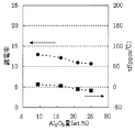
- Sintering shrinkage of the amount and the dielectric ceramic composition of B 2 O 3 is a diagram showing the relationship between thermal expansion coefficients. It is an interface observation photograph after sintering of the high dielectric layer (sintered body of a dielectric ceramic composition) of a multilayer dielectric substrate, and other dielectric layers. It is an observation photograph of a high dielectric material layer. It is a line analysis result in the interface of a high dielectric material layer and other dielectric material layers. It is a line analysis result in the interface of a high dielectric material layer and other dielectric material layers.
- the dielectric ceramic composition of the present invention is mainly composed of a low temperature sintering component and an inorganic filler component.
- the low temperature sintering component is a glass component capable of crystallizing the AAl 2 Si 2 O 8 phase as a crystalline phase after firing. By crystallizing the AAl 2 Si 2 O 8 phase as a crystalline phase after firing, it has high strength and a high quality factor (Q value) at 1 to 5 GHz, and a low thermal expansion coefficient at 40 to 600 ° C.
- the low temperature sintering component used in the present invention contains A, Al, Si as a main component and further contains B, and optionally contains an element consisting of at least one of Na, K, Cu, Mn, Bi, Ag.
- the inorganic filler contains an ATiO 3 (A is an element composed of at least one of Ca and Sr) phase.
- the dielectric constant of the dielectric ceramic composition of the present invention containing the ATiO 3 phase is 10 or more, and the dielectric constant It is possible to make the capacitive element smaller with respect to one with a lower
- the inorganic filler component used in the present invention contains an A element consisting of at least one of Sr and Ca as main composition and Ti, and optionally, an element of rare earth consisting of at least one of Nd, La and Sm, an element of Mg and Zn It is included.
- the dielectric ceramic composition of the present invention is a dielectric ceramic composition containing an ATiO 3 phase and an AAl 2 Si 2 O 8 phase by mixing and using a low temperature sintering component and an inorganic filler component, It can be fired at a temperature of 1000 ° C. or less, and has a dielectric constant of 10 or more in the frequency range of 3 GHz, further 1 GHz to 5 GHz, and a thermal expansion coefficient of less than 7 ppm / ° C. in the temperature range of 40 to 600 ° C.
- a dielectric ceramic composition can be constructed.
- the dielectric ceramic composition of the present invention can be produced as A'Al 2 Si 2 O by using 50 to 80% by weight of a glass component capable of crystallizing AAl 2 Si 2 O 8 phase after firing as a low temperature sintering component. Component diffusion can be suppressed when producing a laminate integrated with a dielectric ceramic composition having eight phases and an Al 2 O 3 phase, and deterioration of the dielectric properties of the dielectric ceramic composition of the present invention can be suppressed. .
- the dielectric ceramic composition of the present invention also has a thermal expansion coefficient of less than 7 ppm / ° C., the dielectric ceramic composition according to the present invention and the A′Al 2 Si 2 O 8 phase and the Al 2 O 3 phase When a laminate integrated with the dielectric ceramic composition having the same is produced, generation of cracks can be suppressed.
- the dielectric ceramic composition having A'Al 2 Si 2 O 8 phase and Al 2 O 3 phase in its structure has a dielectric constant of about 8 in the frequency range of 1 GHz to 5 GHz, so the dielectric ceramic composition according to the present invention
- the dielectric ceramic composition according to the present invention By setting the dielectric constant at 3 GHz of the composition to 10 or more and interposing the dielectric ceramic composition having the A'Al 2 Si 2 O 8 phase and the Al 2 O 3 phase in the structure, the capacitive element is formed. It becomes possible to make it compact.
- the thermal expansion coefficient at 600 ° C. is desirably 7.0 ppm / ° C. or less.
- the AAl 2 Si 2 O 8 phase is substantially the SrAl 2 Si 2 O 8 phase.
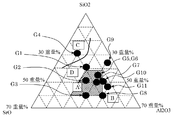
- the characteristics of the low temperature sintering component change according to the ratio of three components of SrO, Al 2 O 3 and SiO 2 .
- a composition having a composition in this range tends to densify when held at 900 ° C. for 2 hours as compared with a composition in the range of (B).
- the composition around the range of (D) is less likely to form the SrAl 2 Si 2 O 8 phase.
- B is an element that exerts an effect on sinterability, and it is preferable to contain 1.5 to 5% by weight.
- the composition of the low temperature sintering component used in the present invention is at least 18 to 40 wt% of Al, Si, Sr, and B respectively in terms of Al 2 O 3 , 40 to 58 wt% in terms of SiO 2 and in terms of SrO. It is preferable that the composition contains 10 to 40% by weight and 1.5 to 5 weight in terms of B 2 O 3 .
- B is a powerful element that can be fired at a low temperature as a single element, and is an essential element in the present invention.
- the amount of Al is preferably 20 to 35% by weight in terms of Al 2 O 3 , and more preferably 22 to 33% by weight.
- the amount of Si is preferably 42 to 55% by weight in terms of SiO 2 , and more preferably 43 to 50% by weight.
- the amount of Sr is preferably 12 to 35% by weight in terms of SrO, and more preferably 13 to 30% by weight.
- the amount of B is preferably 1.2 to 4.5% by weight, more preferably 1.3 to 4.0% by weight, in terms of B 2 O 3 .
- the Bi 2 O 3 preferably 0.1 to 4.5 wt%, more preferably 1 to 4.0 wt% of Na 2 O, the K 2 O 0.2 ⁇ 2 wt%, a CuO 0.2 It is preferable to adjust the amount to 2% by weight, 0.2 to 2% by weight of Mn 3 O 4 and 1 to 4.0% by weight of Bi 2 O 3 .
- Ag when the co-firing with other dielectric layers to be described later is performed, the crack generation rate can be reduced, and the yield at the time of firing can be improved. In addition, a low temperature sintering effect can be obtained.
- the low temperature sintering component be calcined at 600 ° C. or more and 850 ° C. or less. If the temperature is less than 600 ° C., the degree of vitrification is insufficient. If the temperature exceeds 850 ° C., the sintered density is too high and it becomes difficult to finely grind it. It becomes difficult to obtain a desired thermal expansion coefficient. In addition, low temperature firing becomes difficult.
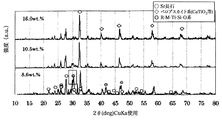
- the low temperature sintering component having the above composition has substantially no SiO 2 phase or SrSiO 3 phase. These phases are not detected even if XRD analysis (using a Cu-K ⁇ tube, voltage 40 mV, current 100 mA) is performed in the state of a sintered body, and around 28 degrees of Sr feldspar (SrAl 2 Si 2 O 8 phase) With respect to the maximum peak value, the peak value of the SiO 2 phase seen near 22 ° and the peak value of the SrSiO 3 phase seen near 31 ° have a height of 1/10 or less.
- the inorganic filler component contains an ATiO 3 (A is an element consisting of at least one of Ca and Sr) phase.
- a element and Ti are respectively converted to AO and TiO 2 , 10 to 60% by weight of AO and 30 to 60% by weight of TiO 2
- the composition contains
- the element A is Ca
- the Ca is preferably 10 to 45% by weight in terms of CaO.
- Sr amount is the amount of 60 wt% or less can suppress the increase of the temperature coefficient tau f of the resonance frequency.
- the rare earth element R (R is Nd, La, elements of one or more Sm) is preferably the addition of 0.01 to 50 wt%.
- Nd 2 O 3 is preferably 1 to 36% by weight.
- the content of La 2 O 3 or Sm 2 O 3 is preferably 1 to 40% by weight. It is desirable to add MgO in the range of 0 to 15% by weight and ZnO in the range of 0 to 10% by weight. If the amount of these components does not exceed this range, the decrease in dielectric constant can be minimized.
- a ' consists of at least one of Ca, Sr, and Ba
- a ' consists of at least one of Ca, Sr, and Ba
- the temperature of the main firing after mixing is preferably more than 750 and less than 1100 ° C.
- the holding time at the sintering temperature is preferably 0.1 to 100 hours, more preferably 0.5 to 10 hours, and further preferably 1 to 5 hours. If the holding time of sintering is short, the low temperature sintering component and the inorganic filler component do not sinter sufficiently. Conversely, if the holding time is long, the additive element on the inorganic filler side will diffuse to the low temperature sintering component side, and it will not be possible to ensure the desired dielectric properties.
- the temperature of the main sintering after being mixed with the low temperature sintering component can be lowered. If the temperature of the pre-sintering is less than 600 ° C., the main-baking tends to be a fired body of pores including pores, and there is a problem in the sinterability.
- the temperature is preferably 650 ° C., more preferably 700 ° C. or more.
- the inorganic filler component be temporarily calcined at more than 850 ° C. and 1300 ° C. or less. If the temperature of temporary firing is over 850 ° C., the temperature of main firing can be set to 1000 ° C.
- the temperature of the preliminary firing is more preferably 1200 ° C. or less.
- the low temperature sintering component and the inorganic filler component are mixed to obtain the dielectric ceramic composition of the present invention, it is shaped into a substrate. Details will be described later.
- This firing can be performed simultaneously with ceramic green sheets using other dielectrics.
- the temperature of this co-firing (main firing) is higher than the pre-firing temperature of the low temperature sintering component and lower than the pre-firing temperature of the inorganic filler component. If it is lower than the pre-sintering temperature of the low temperature sintering component, it can not be combined with other dielectric layers having the same sintering temperature and can not be laminated and integrated.
- the temperature of the main firing is higher than the pre-sintering temperature of the inorganic filler component, the temperature is higher than the melting point of the Ag conductor paste, the Ag paste melts, and desired elements and electrodes can not be formed in the laminate.
- the preferred temperature for the main firing which is influenced by the composition of the other dielectric layers, is more than 850 ° C. and less than 1000 ° C.
- composition of the dielectric ceramic composition of the present invention in which the filler components are combined includes B as an additive element in addition to the main components Al, Si, A, and Ti, and the Al element is 11 in Al 2 O 3 conversion.
- B As an additive element in addition to the main components Al, Si, A, and Ti, and the Al element is 11 in Al 2 O 3 conversion.
- % To 25 wt%, Si element 20 to 33 wt% in SiO 2 conversion, A element 5 to 30 wt% in AO conversion, B element 0.
- Al (Al 2 O 3 conversion) in B 2 O 3 conversion It is preferable that at least 06 times and up to 5% by weight, the remainder include TiO 2 (including unavoidable impurities).
- B is added to the dielectric ceramic composition for crystallizing the AAl 2 Si 2 O 8 phase, the sinterability can be improved while suppressing the decrease in the dielectric constant as much as possible.
- a further preferable composition is 11.5 to 23% by weight in terms of Al 2 O 3 , 22 to 32% by weight in terms of SiO 2 , 7 to 29% by weight of element A in terms of AO, and 1.0 in terms of B 2 O 3 ⁇ 2.5 wt%, balance TiO 2 (including unavoidable impurities), more preferable composition is 12.0 to 20 wt% in terms of Al 2 O 3 , 24 to 31 wt% in terms of SiO 2 , element A Is 7 to 28% by weight in terms of AO, 1.3 to 2% by weight in terms of B 2 O 3 , and the balance is TiO 2 (including unavoidable impurities).
- the Sr element is preferably 5 to 30% by weight in terms of SrO.
- the entire dielectric ceramic composition contains both Sr and Ca.
- the total of SrO and CaO be 5 to 30% by weight in 5 to 15% by weight in terms of SrO.
- Ca is preferably contained in the range of 3 to 18% by weight in terms of CaO.
- the addition of Nd is the easiest to reduce the temperature coefficient ⁇ f .
- the dielectric ceramic composition as a whole 100 parts by weight, Nd, La, Sm, Mg, at least one of Zn, 0.1 ⁇ 20% by weight Nd 2 O 3 in terms of, in La 2 O 3 in terms of 0 It is preferable to contain 1 to 12% by weight, 0 to 12% by weight in terms of Sm 2 O 3 , 0 to 10% by weight in terms of MgO, and 0 to 5% by weight in terms of ZnO.
- a further preferable Nd amount is 1 to 18% by weight in terms of Nd 2 O 3 .
- reduction in temperature coefficient ⁇ f may be achieved using Mg and Zn, which have relatively price fluctuations, and even if rare earth is combined with Mg and Zn. Good.
- the dielectric ceramic composition according to the present invention contains at least one of Na, K, Cu, Mn, and Bi in an amount of 0 to 4 in terms of Na 2 O based on 100 parts by weight of the entire dielectric ceramic composition.
- % 0-1% by weight K 2 O in terms of 0.1 to 3 wt% in terms of CuO, Mn 3 O 4 0.1 to 3 wt% in terms, Bi 2 O 3 1 ⁇ 5 wt% in terms of content Preferred.
- K 2 O in terms of 0.1 to 3 wt% in terms of CuO
- Mn 3 O 4 0.1 to 3 wt% in terms
- CuO and Mn 3 O 4 have an effect of promoting Sr feldspar crystallization.
- 0.1 to 3% by weight of Ag is contained with respect to 100 parts by weight of the whole dielectric ceramic composition.
- Ag is contained in the other dielectric layers, it is possible to suppress the occurrence of cracks during co-firing with the layers.
- migration can be suppressed when a conductor made of Ag or Ag alloy paste is used for the dielectric layer using the dielectric ceramic composition.
- the dielectric ceramic composition having the above composition is an R-M-Ti-Si-O system (R is an element composed of at least one of Nd, Sm and La, and M is at least one of Mg and Zn) It is characterized in that the phase of the following element) or the phase of the A-Ti-Si-O system (A is an element consisting of at least one of Ca and Sr) does not substantially exist.
- the phase of the R-M-Ti-Si-O system corresponds to, for example, the M 2 R 4 Ti 3 Si 4 O 22 phase.
- the phase of the A-Ti-Si-O system corresponds to, for example, a CaTiSiO 5 phase or a Sr 2 TiSi 2 O 8 phase.
- phase of the R-M-Ti-Si-O system When the phase of the R-M-Ti-Si-O system remains, the thermal expansion coefficient tends to increase, and when the A-Ti-Si-O phase remains, the quality factor fQ tends to deteriorate. This phase is not detected even when XRD analysis (using a Cu-K ⁇ tube, voltage 40 mV, current 100 mA) is performed in the state of the sintered body, and 33 degrees of Sr feldspar (AAl 2 Si 2 O 8 phase)
- the peak value of the phase of the R-M-Ti-Si-O system observed near 30 degrees with respect to the maximum peak value in the vicinity is 1/10 or less the height (intensity ratio 10% or less).
- the multilayer dielectric substrate according to the present invention is a multilayer dielectric substrate in which a plurality of dielectric layers having a conductor formed thereon are laminated and integrated.
- the plurality of dielectric layers at least one dielectric layer is formed using the dielectric ceramic composition according to the present invention (this dielectric layer is also referred to as a high dielectric constant layer), and the other dielectric layers are single.
- a dielectric ceramic composition having a diagonal AAl 2 Si 2 O 8 phase and an Al 2 O 3 phase is used (this dielectric layer is also referred to as a low dielectric constant layer).
- the high dielectric constant layer may be a single layer or a plurality of layers. That is, when the high dielectric constant layer is a single layer, it is preferable to arrange the high dielectric constant layer substantially at the center in the stacking direction, and when there are multiple high dielectric constant layers, it is preferable to divide the high dielectric constant layer on both sides . In the case where there are a plurality of high dielectric constant layers, it is more preferable to dispose the high dielectric constant layers in the same order from the upper surface and the lower surface.
- the other dielectric ceramic compositions having the above-mentioned AAl 2 Si 2 O 8 phase and Al 2 O 3 phase are, for example, Al 2 O 3 , SiO 2 , SrO which are the main components Al, Si, Sr, and Ti, respectively.
- 10 to 60% by weight of Al 2 O 3 , 25 to 60% by weight of SiO 2 , 7.5 to 50% by weight of SrO, 20% by weight or less (including 0) of TiO 2 when converted to TiO 2 are those containing 2, as an auxiliary component, Bi, Na, K, at least one selected from the group of Co, for its main component 100 parts by weight, 0-10% by weight in terms of Bi 2 O 3, 0 to 5% by weight in terms of Na 2 O, 0 to 5% by weight in terms of K 2 O, 0 to 5% by weight in terms of CoO, and at least one of the groups Cu, Mn, Ag Cu in terms of CuO is 0 to 100 parts by weight of the main component Wt%, 0-5 wt% of Mn in Mn 3 O 4 conversion, the Ag containing 0-5 wt%, a mixture containing unavoidable impurities once calcined at 700 ° C.
- the other dielectric ceramic composition contains 0.01 to 5% by weight of Ag, it is preferable that Ag is also added to the dielectric ceramic composition of the present invention.
- each element is as follows: 0.1 to 8% by weight in terms of Bi 2 O 3 and 0.1 to 4% in terms of Na 2 O of at least one of the groups Bi, Na, K, Co %, 0.1 to 3% by weight in terms of K 2 O, 0.1 to 3% by weight in terms of CoO, and at least one of the groups Cu, Mn, Ag, and Cu for Cu 0.01 to 3% by weight, 0.01 to 3% by weight in terms of MnO 2 in terms of Mn, and 0.01 to 3% by weight Ag on Ag.
- Bi has an effect on low temperature firing.
- a plurality of high dielectric constant green sheets made of the dielectric ceramic composition of the present invention are generated.
- a slurry consisting of a powder of the dielectric ceramic composition and a mixture of an organic binder, a plasticizer and a solvent is formed into a film having a predetermined thickness on an organic carrier film (for example, a PET film) by a doctor blade method and dried.
- the thickness after drying of the dielectric ceramic composition slurry is appropriately designed to be a preferable thickness for using the multilayer dielectric substrate as a capacitor built-in substrate.
- a plurality of low dielectric constant green sheets composed of other dielectric layers are also generated.
- a slurry comprising a mixture of the powder of the other dielectric ceramic composition and the powder of the glass component, the organic binder, the plasticizer, and the solvent is formed into a film having a predetermined thickness by a doctor blade method and dried.
- the thickness after drying of the other dielectric layer slurry varies depending on the thickness of the multilayer dielectric substrate, the circuit configuration, and the like, it is generally 20 to 200 ⁇ m.
- the generation of the high dielectric constant green sheet and the low dielectric constant green sheet is not limited to the doctor blade method described herein, and may be generated by, for example, rolling (extrusion) method, printing method, ink jet coating method, transfer method, etc. May be At this time, the high dielectric constant green sheet and the low dielectric constant green sheet form a ceramic green sheet with a carrier film integrally formed on a thin carrier film such as a PET film. And it does not peel from a carrier film, but it cut
- via holes are formed in the high dielectric constant green sheet and the low dielectric constant green sheet with each carrier film using a laser according to the target circuit.
- a conductor paste containing silver (Ag) as a main component is disposed in each via hole through the printing screen, the conductor paste is pressed into the via hole with a squeegee, and excess conductor paste is peeled off.
- the green sheet is mounted on the support of the printing apparatus so that the green sheet is on the printing screen side and the carrier film is on the support side, and the printing and filling process of the via electrodes is performed.
- a conductive paste such as silver (Ag) is used on the surface of each green sheet including the low dielectric constant green sheet 2a on the upper surface to make the electrode pattern 4 corresponding to the target circuit 5 to 35 ⁇ m thick.
- These electrode patterns 4 form internal wiring such as an inductor, a transmission line, a capacitor, a ground electrode and the like, and they are connected to each other by via wiring by the via electrodes to constitute a target circuit wiring.
- a high dielectric constant green sheet and a low dielectric constant green sheet on which via electrodes and / or conductor patterns are formed are appropriately laminated.
- the high dielectric constant green sheets 3a, 3b, 3c and 3d often serve as layers for forming a capacitor, and usually serve as a mid-portion layer of a multilayer dielectric substrate.
- the low dielectric constant green sheets 2a, 2b, 2c and 2d are preferably formed relatively thick and disposed in the outermost layer.
- a multilayer green sheet in which the high dielectric constant green sheet and the low dielectric constant green sheet are appropriately stacked is press-bonded by pressing, and the step of peeling the carrier film is repeated by the number of ceramic substrate layers to laminate an unsintered multilayer ceramic laminate (Hereinafter, simply referred to as "green multilayer dielectric substrate”) is produced.
- the low dielectric constant green sheet 2a with a carrier film of the first layer to be positioned on the outermost surface side of the non-sintered multilayer dielectric substrate is inverted on the carrier film side up and set on the fixing film Press and press with a mold at a predetermined pressure, temperature and time.
- the pressure is 1 to 5 MPa (10 to 51 kgf / cm 2 )
- the temperature is 30 to 60 ° C.
- the time is 3 to 15 seconds.
- the thermocompression bonding upper and lower molds may be a simple flat plate shape incorporating a heater.
- the low dielectric constant green sheet 2a is fixed to the fixing film, and is not peeled off together when the carrier film is peeled off.
- the laser wavelength for forming the via holes is appropriately selected and small via holes are formed so that continuous through via holes are not formed in the carrier film, the low dielectric constant green sheet 2a of the carrier film is peeled off. It becomes difficult to pull out the conductor paste filled in the via holes together, and as a result, it is possible to prevent the occurrence of conduction failure due to the disconnection of the via wiring.
- the second high dielectric constant green sheet 3a is laminated.
- the high dielectric constant green sheet 3a is printed with a conductor pattern constituting an internal circuit wiring.
- the main surface of the ceramic green sheet 3a is set to abut on the low dielectric constant green sheet 2a of the first layer, and pressing and pressure bonding are performed as in the case of the low dielectric constant green sheet of the first layer.
- the pressing temperature is set to a temperature at which the adhesive in the printing paste softens and adheres
- the printing unit is joined to the opposing green sheet 2a by the pressure. Therefore, the green sheets are bonded to each other through the printed conductor paste.
- the pressure bonding temperature at this time depends on the type of the adhesive, but it may be a low temperature of about 40 to 90 ° C., and the bonding strength can be adjusted by changing the pressure.
- the carrier film of the high dielectric constant green sheet 3a is peeled off. From the high dielectric constant green sheet 3b of the third layer to the low dielectric constant green sheet corresponding to the outermost layer on the back (bottom) surface side, lamination is performed in the same process as the high dielectric constant green sheet of the second layer.
- a conductive paste mainly composed of Ag is used on the bottom surface of the non-sintered multilayer dielectric substrate thus obtained (the opposite surface facing the surface of the outermost ceramic substrate layer).
- the surface electrode on the bottom side is printed and formed according to the circuit of
- an overcoat material may be suitably formed around the conductor patterns on the substrate surface and the bottom surface.
- a material of the overcoat material it is desirable that the sintering shrinkage characteristics and the thermal expansion characteristics are similar to the material of the green multi-layer dielectric substrate.
- a slurry of the same material as that of the ceramic green sheet to which an additive component for imparting a function to improve the visibility of the coated part is added.
- the green multi-layer dielectric substrate thus obtained is thermocompression bonded at 10-40 MPa (100-400 kgf / cm 2 ) at 85 ° C. in a CIP device, and the layers are integrated into a green sheet. It is a multilayer dielectric substrate.
- notches are formed on the surface of the non-sintered multilayer dielectric substrate with a jig such as a knife cutter to form dividing grooves.
- the dividing grooves are formed in different shapes depending on the size of the collective substrate and the size of the product substrate.
- the dividing grooves are formed with a sufficient dimension so as not to adversely affect the conductor patterns constituting the circuit, and are formed at a distance of about 100 to 250 ⁇ m from the end of the conductor in plan view.
- This dividing groove is, for example, a V-shaped groove, and the depth is, for example, 30% or less of the thickness of the non-sintered multilayer dielectric substrate when the dividing grooves are put on the upper and lower surfaces.
- the dividing grooves do not necessarily have to be formed on both sides, and either the upper surface or the bottom may be used.
- the division method is not limited to the method of dividing along the V-shaped groove, but may be a method of dicing or scribing after the subsequent baking process without forming the groove.
- the unsintered multilayer dielectric substrate is subjected to integral firing at a sintering temperature of 800 to 1000 ° C. in a firing furnace. Thereafter, etching treatment to the surface layer via electrode, metal plating film forming treatment such as electroless plating, and the like are performed as necessary.
- Electrodes When such a multilayer dielectric substrate is used, surface mount components are mounted on the surface of the metal plating layer 3 using solder balls to constitute an electronic component.
- This electronic component can be used, for example, in an electronic device such as a mobile phone.
- electronic components to be mounted include passive elements such as capacitors, inductors and resistors, semiconductor products, and active elements such as module parts including an array in which a plurality of passive parts are integrated.
- passive elements such as capacitors, inductors and resistors, semiconductor products, and active elements
- module parts including an array in which a plurality of passive parts are integrated.
- Such electronic components are, for example, dielectric resonators, filters, multilayer capacitors, antenna switch modules, front end modules, and the like.
- the low temperature sintering component weighs an iodine raw material having a target composition, dries the mixed material, and temporarily calcinates the obtained powder.
- the reaction of the raw material may be advanced to partially vitrify by setting the pre-baking temperature appropriately.
- the powder obtained by thus pre-baking is pulverized by a method such as a ball mill to obtain a low temperature sintered component powder.
- the inorganic filler component is obtained by weighing and mixing the raw materials so as to achieve the target composition, and the obtained powder is temporarily calcined to contain ATiO 3 (A is an element consisting of at least one of Ca and Sr) phase A calcined powder is obtained.
- the powder is pulverized to obtain an inorganic filler powder.
- the powder obtained by mixing the low-temperature sintered powder thus obtained and the inorganic filler powder in an appropriate ratio is granulated, shaped and fired to obtain a desired sintered body.
- the inorganic filler component does not necessarily have to be calcined.
- a sintered body may be obtained by mixing the inorganic filler component with the low-temperature sintering component powder without performing temporary firing, granulating and forming, and firing.
- a desired crystal (ATiO 3 (A is an element consisting of at least one of Ca and Sr) phase) precipitates, and if desired characteristics can be obtained, the inorganic filler or the like subjected to temporary calcination as described above is mixed
- a mixture of the raw material of the low temperature sintering component and the raw material of the inorganic filler component may be calcined and crushed. If such a method can be applied, it is more desirable because the process is simplified.
- the density of the sintered body was determined by measuring the size of the sample with a micrometer, weighing it with an electronic balance, and calculating it from these values.
- the sintering shrinkage rate was calculated by measuring each of the samples before and after sintering with a micrometer.
- the dielectric properties were determined using a network analyzer (manufactured by HEWLETT PACKARD, 8720D) by a method using a cylindrical resonator (based on JIS R1627). The dielectric constant was measured using a 25 ° C. sample.
- the thermal expansion coefficient was determined by the method according to JIS R1618.
- the XRD (X-Ray Diffraction X-ray Diffraction) analysis was carried out under the conditions of a voltage of 40 mV and a current of 100 mA using a Cu-K ⁇ tube in the state of a sintered body without pulverizing each sintered body.
- the raw materials are weighed, mixed, and mixed so as to have the composition shown in Table 1 as a low-temperature sintering component, and the powder obtained by mixing is temporarily fired at 750 ° C. and pulverized to a particle size of 1 ⁇ m or less
- the powder of the low temperature sintering component was produced.
- raw materials for SrO, Na 2 O and K 2 O, SrCO 3 , Na 2 CO 3 and K 2 CO 3 were used, respectively.
- As an inorganic filler component after weighing and mixing so that it may become composition of Table 2, it pre-baked at 1100 degreeC, this was grind
- CTO is CaTiO 3 phase
- STO is SrTiO 3 phase
- NTO is Nd 2/3 TiO 3 phase
- LTO is La 2/3 TiO 3 phase
- SmTO is Sm 2/3 TiO 3 phase
- MZTO It refers to a Mg ⁇ Zn) 2 TiO 4 phase.
- the dielectric characteristics were evaluated by the dielectric resonator method (JIS R1627) using the obtained sample.
- JIS R1627 The thermal expansion coefficient, a cylindrical sample having a diameter of 3 mm and a height of 8 mm was prepared, and the thermal expansion coefficient (40 to 600 ° C.) was measured by TMA 8140 manufactured by Rigaku.
- Table 3 The results are shown in Table 3.
- the samples marked with an asterisk in Tables 3 and 4 indicate that they are out of the range of the dielectric ceramic composition according to the present invention.
- Low temperature sintering components G2 and G6 to G8 containing an inorganic filler component of F1 to F22 containing ATiO 3 phase and a glass component capable of crystallizing SrAl 2 Si 2 O 8 phase as a crystal phase after firing A dielectric ceramic composition which can be fired at a temperature of 1000 ° C. or less and which has a dielectric constant of 10 or more in a frequency range of 1 GHz to 5 GHz and a thermal expansion coefficient of less than 7 ppm / ° C. in a temperature range of 40 to 600 ° C. It has been realized (No. 2, No. 6 to 8, No.
- the sintered body density is saturated at a temperature of at least 900 ° C., and densification at such temperature is possible.
- the samples of No. 1 and No. 11 using G1 and G11 they reacted with the filler and the thermal expansion coefficient increased to 7 ppm / ° C. or more.
- the dielectric characteristics could not be measured. It is also possible to control the thermal expansion coefficient to 6 ppm / ° C. or less by appropriately combining the inorganic filler component and the low temperature sintering component (No. 15, No. 21, No. 22).
- a sample containing RTiO 3 (R is at least one of Nd, La, and Sm) by containing Nd, La, and Sm, and an M 2 TiO 4 (M is Mg) by containing Mg and / or Zn.
- R is at least one of Nd, La, and Sm
- M is Mg
- the absolute value of the temperature coefficient ⁇ f of the resonance frequency is smaller in the sample containing at least one of Zn and Zn (No. 12 and No. 19) not including these.
- Absolute value 120 ppm / ° C. or less of the dielectric ceramic composition of the temperature coefficient tau f of the resonant frequency by controlling these additives and the like are realized.
- each phase (CaTiO 3 , SrTiO 3 , Nd 2/3 TiO 3 , La 2/3 TiO 3 , Sm 2/3 TiO 3 , (Mg ⁇ Zn) 2 TiO 4, which is an inorganic filler component, is a dielectric. It also remains in the porcelain composition.
- the blending amounts of the low temperature sintering component and the inorganic filler component were examined.
- G6 shown in Table 1 was used as the low temperature sintering component.
- F2 shown in Table 2 was used as the inorganic filler.
- Table 5 shows the relationship between the content of the inorganic filler component, the dielectric constant, and the densification temperature.
- the dielectric constant rises with the increase of the mixing amount of the inorganic filler component, and one having a high dielectric constant can be manufactured at 40 wt% or more.
- the mixing ratio is preferably 45 to 75:25 to 55, more preferably 50 to 70:30 to 50, for the low temperature sintering component: inorganic filler.
- FIG. 3 shows sample No. 1 of Table 1. It is the result of measuring the sintered compact of the low temperature sintering component of G1 by XRD (X-Ray Diffraction X-ray diffraction). The sintering temperature is 750. The measurement conditions of the XRD were a Cu-K ⁇ tube, a current density of 100 ⁇ A, and a voltage of 40 mV. From the analysis from the peak angle, it was confirmed that SrSiO 3 and SiO 2 were precipitated in addition to Sr feldspar.
- SrSiO 3 and SiO 2 are precipitated as SrSiO 3 and SiO 2 .
- the thermal expansion coefficient of SrSiO 3 is 10.3 ppm / ° C., and the precipitation of the same component causes an increase in the thermal expansion coefficient.
- SiO 2 is known to exhibit anomalous volume change of about 1% due to phase change in the vicinity of 100 ° C. to 200 ° C., which may contribute to an increase in the thermal expansion coefficient.
- SrSiO 3 and SiO 2 can be suppressed by increasing Al 2 O 3 in the low temperature sintering component and promoting the precipitation of Sr feldspar.
- FIG. 4 shows the low-temperature sintered component of the amount of Al 2 O 3 and 40 wt.
- FIG. 6 shows the XRD pattern of the% mixed dielectric composition.
- the Sr feldspar main peak is the largest and appears at 32.8 °.
- FIG. 4 shows the low-temperature sintered component of the amount of Al 2 O 3 and 40 wt.
- FIG. 6 shows the XRD pattern of the% mixed dielectric composition.
- the Sr feldspar main peak is the largest and appears at 32.8 °.
- FIG. 6 shows the relationship between the sintering shrinkage and the coefficient of thermal expansion of the mixture sintered at 900 ° C. and the amount of Al 2 O 3 .
- FIG. 7 shows the relationship between the dielectric constant of the mixed material fired at 900 ° C., ⁇ f , and the amount of Al 2 O 3 .
- the thermal expansion coefficient of the mixture decreases with the increase of the amount of Al 2 O 3 of the low temperature sintering component, and can be 7 ppm / ° C. or less if the amount of Al 2 O 3 is 11.0 wt% or more.
- FIG. 8 shows the thermal characteristics of the mixed material in which the amount of B 2 O 3 in the low temperature sintering component is changed.
- the amount of B 2 O 3 increases, the sintering shrinkage rate increases and the dielectric constant increases.
- ⁇ f and the thermal expansion coefficient do not change even if the B 2 O 3 amount is added.
- the amount of B 2 O 3 is more than 3 wt%, the binder and the cross-linked structure are formed to deteriorate the formability, so the content is preferably 3 wt% or less.
- a ceramic layer made of a dielectric ceramic composition and another dielectric layer were formed, and were simultaneously fired in the laminated state, and the presence or absence of cracks and delamination was confirmed between the two.
- evaluation was performed using the dielectric ceramic composition having the composition shown in Table 6 and other dielectric layers.
- the sample No. shown in Tables 3 and 4 The dielectric ceramic composition having the composition 14 was introduced into a polyethylene ball mill, wet-grounded for 17 hours, and then dried to obtain a fine powder having an average particle diameter of 1 ⁇ m.
- calcined powders of other dielectric layers were obtained as follows. Materials having the compositions shown in Table 6 were charged into a polyethylene ball mill, and media balls made of zirconium oxide and pure water were further charged and wet mixed for 20 hours. The obtained slurry was dried by heating, then crushed by a lai-kai machine, placed in an alumina crucible, and calcined at 800 ° C. for 2 hours. The obtained calcined body was put into the above-mentioned ball mill, wet-grounded for 17 hours, and then dried to obtain a fine powder having an average particle diameter of 1 ⁇ m. The subsequent steps are the same to produce both ceramic green sheets.
- slurry was prepared by mixing. No dispersant was added. The slurry was degassed under reduced pressure and ethanol was partially evaporated to adjust the viscosity to about 7 Pa ⁇ s. The slurry was formed into a sheet on a PET carrier film by a doctor blade method, and dried to obtain a substrate green sheet having a thickness of 0.04 mm. The substrate green sheet was cut into 180 mm square together with the carrier film.
- DOP bis (2-ethylhexyl) phthalate
- an internal electrode pattern and an external electrode pattern 4 were formed of a conductive paste mainly composed of Ag, and via electrodes 5 connecting the electrode patterns were appropriately provided.
- the green sheet is obtained by using the same production method, together with green sheets 2a, 2b, 2c and 2d of a dielectric ceramic composition having an AAl 2 Si 2 O 8 phase and an Al 2 O 3 phase after sintering. As shown in FIG. 2, lamination and pressure bonding were performed to obtain an unsintered multilayer dielectric substrate.
- the non-sintered multilayer dielectric substrate was pressed with a knife blade to form dividing grooves 5 having a width of 0.15 mm and a cross-sectional shape of an isosceles triangle having a depth of 0.1 mm at intervals of 10 mm ⁇ 15 mm.
- the obtained unfired multilayer ceramic substrate is debindered by holding it at 500 ° C. for 4 hours in the atmosphere using a batch furnace, and then heated to 900 ° C. at a rate of 3 ° C./min. It was sintered by holding for 2 hours and naturally cooled in a furnace. Thereby, a multilayer dielectric substrate of the present invention was obtained.
- the multilayer dielectric substrate thus obtained was polished and observed to determine the presence or absence of cracking and delamination. The results are shown in Table 3.
- Table 4 shows all the compositions of Table 3.
- FIG. 9 is a cross-sectional photograph of the multilayer dielectric substrate of the present invention, wherein the region A at the top of the photograph is a layer made of the dielectric ceramic composition of the present invention and the region B is another dielectric layer.
- the dielectric ceramic composition of the present invention is a mixture of the raw materials so as to have the composition shown in Table 6.
- the compositions of the raw materials used for the other dielectric layers are also described.
- FIG. 10 is an enlarged view of a portion surrounded by a square of the region A of FIG.
- the (1) portion has a composition substantially equivalent to that of the inorganic filler component
- the (2) portion has a composition substantially equivalent to that of the low temperature sintering component.
- FIG. 11 is a result of line analysis of amounts of Sr, Al, and Si elements obtained by measuring the interface between the region A and the region B in the direction perpendicular to the interface. From the layer of the region A made of the dielectric ceramic composition to the region B of the other dielectric layers, the amount of Al rapidly increases in the vicinity of the boundary. Further, FIG. 12 shows the amounts of Nd, Ti and Ca measured in the same manner. Nd and Ca are elements not added to the other dielectric layer side. In the region of the dielectric ceramic composition, the concentration is detected to be approximately equal to the average amount of these elements in the entire dielectric ceramic composition. On the other hand, on the other dielectric layer side, it is hardly detected.
- the part where the elements in both of these are fluctuating is the diffusion layer, and this diffusion layer has a thickness of 20 ⁇ m or less at the boundary part.
- the diffusion layer is 20 ⁇ m or less, preferably 10 ⁇ m or less, an excellent multilayer dielectric substrate having both the characteristics of the inorganic filler component and the low temperature sintering component can be obtained.
- the low-temperature sintering component and the inorganic filler component were not produced by pre-sintering at different temperatures, respectively, but were directly fired from the raw materials to produce a dielectric ceramic composition.
- the sample No. shown in Tables 3 and 4 The raw materials were adjusted so as to have a composition of 2, 7, 14, 15, 27 and charged into a polyethylene ball mill, and further, media balls made of zirconium oxide and pure water were charged and wet mixed for 20 hours.
- the obtained slurry was dried by heating, then crushed by a lai-kai machine, placed in an alumina crucible, and calcined at 800 ° C. for 2 hours.
- the obtained calcined body was put into the above-mentioned ball mill, wet-grounded for 17 hours, and then dried to obtain a fine powder having an average particle diameter of 1 ⁇ m. Thereafter, a sintered body was manufactured in the same manner as the dielectric ceramic composition obtained by temporarily sintering the low temperature sintering component and the inorganic filler component to each other and then obtaining the mixed powder.
- Dielectric constant of sintered body dielectric constant in the frequency range of 1 GHz to 5 GHz, quality factor fQ in 1 to 5 GHz, temperature coefficient of resonant frequency ⁇ f in the temperature range of -20 ° C. to 60 ° C., temperature range of 40 to 600 ° C.
- the coefficient of thermal expansion, sintered product, presence or absence of crack and delamination (the composition of the high dielectric layer is sample No. 14 in Tables 3 and 4) were examined. Table 8 shows the results. Except for the quality factor fQ, substantially equivalent values can be obtained as compared with those obtained by temporarily sintering the low temperature sintering component and the inorganic filler component at different temperatures. Since the quality factor fQ tends to be slightly inferior, if it is desired to obtain a dielectric ceramic composition having high characteristics and a multilayer dielectric substrate, a manufacturing method in which the low temperature sintering component and the inorganic filler component are temporarily fired at different temperatures is used. It is preferable to apply.
Landscapes
- Chemical & Material Sciences (AREA)
- Engineering & Computer Science (AREA)
- Ceramic Engineering (AREA)
- Manufacturing & Machinery (AREA)
- Materials Engineering (AREA)
- Structural Engineering (AREA)
- Organic Chemistry (AREA)
- Inorganic Chemistry (AREA)
- Compositions Of Oxide Ceramics (AREA)
- Inorganic Insulating Materials (AREA)
Abstract
Description
添加元素が上記の組成範囲を満たす事により-20℃~60℃の温度範囲における共振周波数の温度係数τfの絶対値が120ppm/℃以下である誘電体磁器組成物を得ることができる。
さらにはこれを用いた多層誘電体基板および電子部品を提供することができる。
さらには上記誘電体磁器組成物を得るための好ましい製造方法を提供することができる。
一方、無機フィラーとしてはATiO3(AはCa、Srのうち少なくとも一種からなる元素)相を含むものとする。かかるATiO3相は高誘電率(CaTiO3がε=280、SrTiO3がε=170)であるため、ATiO3相を含む本発明の誘電体磁器組成物の誘電率を10以上とし、誘電率が低いものに対して容量素子を小型にすることが可能となる。本発明で用いた無機フィラー成分は、主組成としてSrやCaの少なくとも一種からなるA元素と、Tiを含み、必要により、Nd、La、Smの少なくとも一種からなる希土類やMg、Znの元素を含むものである。
本発明の誘電体磁器組成物は、低温焼結化成分と無機フィラー成分を混合して用いることで、ATiO3相とAAl2Si2O8相を含有する誘電体磁器組成物であって、1000℃以下の温度で焼成可能であるとともに、3GHz、さらには1GHz~5GHzの周波数範囲における誘電率が10以上、かつ40~600℃の温度範囲における熱膨張係数が7ppm/℃未満となるように誘電体磁器組成物を構成することができる。
また、Bは焼結性に効果を発揮する元素であり、1.5~5重量%含むことが好ましい。
よって本発明に用いる低温焼結化成分の組成は、少なくともAl、Si、Sr、Bをそれぞれ、Al2O3換算で18~40重量%、SiO2換算で40~58重量%、SrO換算で10~40重量%、B2O3換算で1.5~5重量を含む組成であることが好ましい。特にBは単体で低温焼成が可能とする有力な元素であって本発明では必須の元素である。
Al量はAl2O3換算で20~35重量%が好ましく、22~33重量%がさらに好ましい。
Si量はSiO2換算で42~55重量%が好ましく、43~50重量%がさらに好ましい。
Sr量はSrO換算で12~35重量%が好ましく、13~30重量%がさらに好ましい。
B量はB2O3換算で1.2~4.5重量%が好ましく、1.3~4.0重量%がさらに好ましい。
さらにNa2Oを0.1~4.5重量%、K2Oを0.1~3重量%、CuOを0.1~4重量%、Mn3O4を0.1~3重量%、Bi2O3を0.1~4.5重量%とすることが好ましく、さらにNa2Oを1~4.0重量%、K2Oを0.2~2重量%、CuOを0.2~2重量%、Mn3O4を0.2~2重量%、Bi2O3を1~4.0重量%とすることが好ましい。
さらに、無機フィラー成分は850℃超1300℃以下で仮焼成することが好ましい。仮焼成の温度が850℃超であれば、本焼成の温度を1000度以下、さらには950度以下にすることができる。仮焼成の温度が1300℃超では仮焼成する際の容器との反応が大きくなり不純物元素の混入の原因ともなるし、細かく粉砕することが困難になるのでその後の低温焼結化成分の仮焼成粉と混ぜて本焼成しても、空孔を含むポアの焼成体に成りやすく、焼結性に難がある。仮焼成の温度は1200℃以下がさらに好ましい。
本焼成はその他の誘電体をもちいたセラミックグリーンシートと同時に焼成することができる。
この同時焼成(本焼成)の温度は低温焼結化成分の仮焼成温度より高く、無機フィラー成分の仮焼成温度より低い温度で行なう。低温焼結化成分の仮焼成温度より低ければ、同様の焼結温度を持つその他の誘電体層と結合せず積層一体化できない。他方、本焼成の温度が無機フィラー成分の仮焼成温度より高ければ、Ag導体ペーストの融点以上の温度であるのでAgペーストが溶け流れ、積層体内に所望の素子、電極を形成することができない。
本焼成の好ましい温度は、その他の誘電体層の組成にも影響されるが、850℃超1000℃未満である。
AAl2Si2O8相を晶出させるための誘電体磁器組成物にBを添加すると、誘電率の低下を極力抑制しながら焼結性を向上させることができる。
更に好ましい組成は、Al2O3換算で11.5~23重量%、SiO2換算で22~32重量%、A元素がAO換算で7~29重量%、B2O3換算で1.0~2.5重量%、残部TiO2(不可避不純物を含む)であり、更に好ましい組成は、Al2O3換算で12.0~20重量%、SiO2換算で24~31重量%、A元素がAO換算で7~28重量%、B2O3換算で1.3~2重量%、残部TiO2(不可避不純物を含む)である。
Alが少ないと誘電体磁器組成物中にR-M-Ti-Si-O系の相が発生して熱膨張係数が大きくなりやすい。またAlが多いと焼結性に影響が出て、クラックやデラミネーションが発生しやすい。
A元素(Ca、Srのうち少なくとも一種からなる元素)、特にSrが少ないと焼結過程でSr長石が出ずに他の相が出現し、熱膨張係数が大きくなりやすい。また、A元素が多いと共振周波数の温度係数τfの絶対値を小さくすることができない。A元素が多くてもTiが少なければ長石が析出するためτfの上昇は必ずしもおきないが、Sr元素が15重量%を超える場合はSrとTiの比をSrO/TiO2換算で1.5以上とすることが好ましい。
Sr量とCa量を上記の範囲とすることで、さらに高誘電率、低熱膨張係数、および高い焼結性を持つ誘電体磁器組成物が得やすくなる。
Ndの添加が最も温度係数τfの低下を行ないやすい。誘電体磁器組成物全体を100重量部として、Nd、La、Sm、Mg、Znのうちの少なくとも1種を、Nd2O3換算で0.1~20重量%、La2O3換算で0~12重量%、Sm2O3換算で0~12重量%、MgO換算で0~10重量%、ZnO換算で0~5重量%含有することが好ましい。さらに好ましいNd量はNd2O3換算で1~18重量%である。但し、希土類元素は恒常的に高価であるため、比較的価格変動があるMg、Znを用いて温度係数τfの低下を図ってもよいし、希土類とMg、Znを複合して用いてもよい。
焼結体の状態でXRD分析(Cu-Kα管使用、電圧40mV、電流100mA)を行なってもこの相は検出されず、Sr長石をはじめとする(AAl2Si2O8相)の33度付近での最大ピーク値に対して、30度付近で見られるR-M-Ti-Si-O系の相のピーク値が1/10以下の高さ(強度比10%以下)である。
好ましい各元素それぞれの添加範囲は、Bi、Na、K、Coの群のうちの少なくとも1種をBi2O3換算で0.1~8重量%、Na2O換算で0.1~4重量%、K2O換算で0.1~3重量%、CoO換算で0.1~3重量%含有し、更に、Cu、Mn、Agの群のうちの少なくとも1種を、Cuに関してはCuO換算で0.01~3重量%、Mnに関してはMnO2換算で0.01~3重量%、Agに関してはAgを0.01~3重量%含む。特にBiは低温焼成に効果を持つ。
多層誘電体基板を形成する工程では、まず、本発明の誘電体磁器組成物からなる高誘電率グリーンシートを複数生成する。例えば有機キャリアフィルム(例えばPETフィルム)上に、この誘電体磁器組成物の粉末、及び有機バインダ、可塑剤、溶剤の混合物からなるスラリーをドクターブレード法により所定厚の膜状に形成し、乾燥させる。誘電体磁器組成物スラリーの乾燥後の厚みは、その多層誘電体基板をコンデンサ内蔵基板とするのに好ましい厚みに適宜設計される。
また、その他の誘電体層からなる低誘電率グリーンシートも複数生成する。有機キャリアフィルム上に、その他の誘電体磁器組成物の粉末とガラス成分の粉末及び有機バインダ、可塑剤、溶剤の混合物からなるスラリーをドクターブレード法により所定厚の膜状に形成し、乾燥させる。その他の誘電体層スラリーの乾燥後の厚みは、その多層誘電体基板の厚さ、回路構成等によってそれぞれ異なるが、20~200μmとするのが一般的である。
このような多層誘電体基板を用いるときには、金属めっき層3表面に、半田ボールを用いて表面実装部品を搭載して電子部品を構成する。この電子部品は、例えば携帯電話機などの電子機器に用いることができる。また、実装する電子部品はコンデンサ、インダクタ、抵抗等の受動素子のほか、半導体製品、さらには、複数の受動部品を集積したアレイなどを含んだモジュール部品等の能動素子が挙げられる。かかる電子部品は、例えば、誘電体共振器、フィルタ、積層コンデンサ、アンテナスイッチモジュール、フロントエンドモジュールなどである。

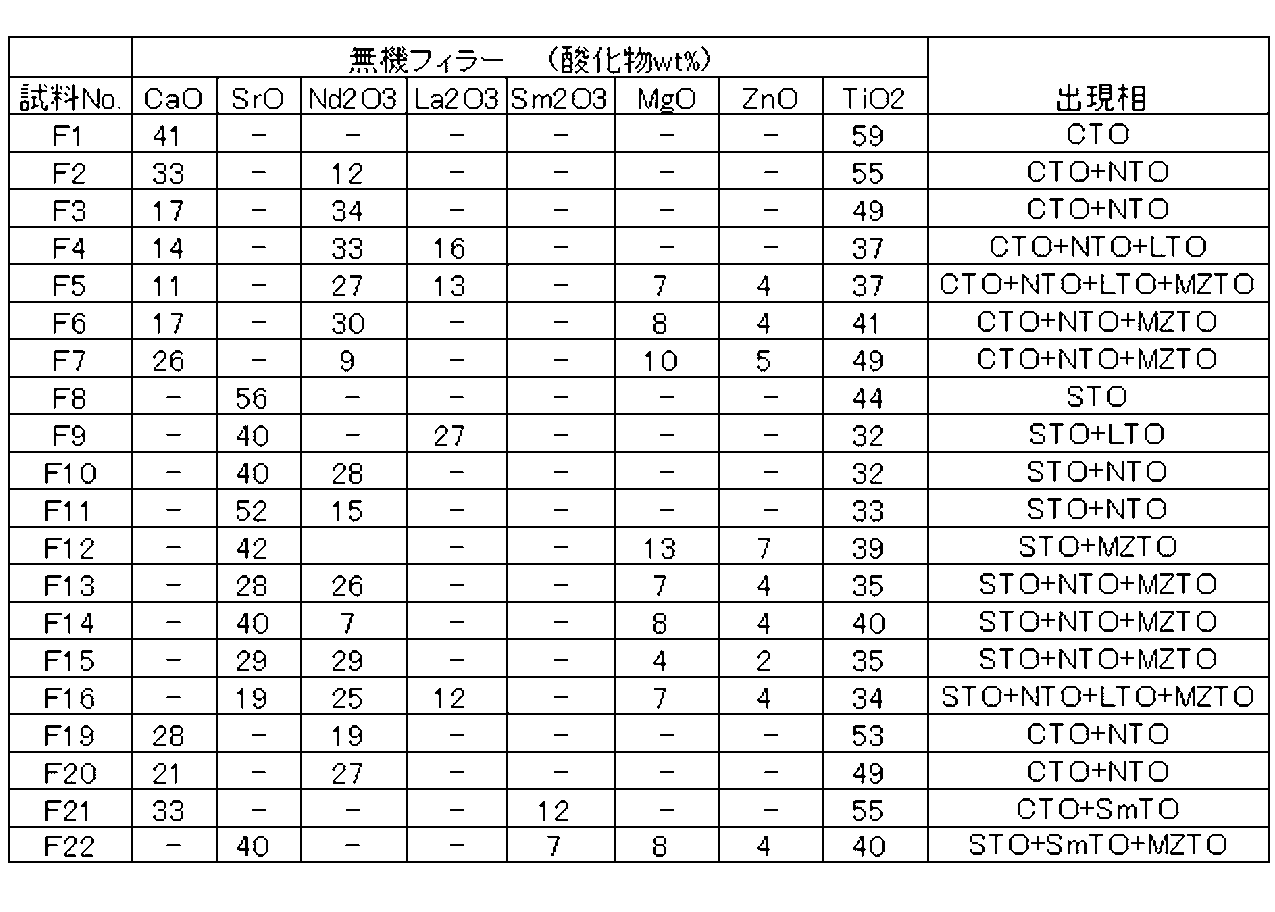
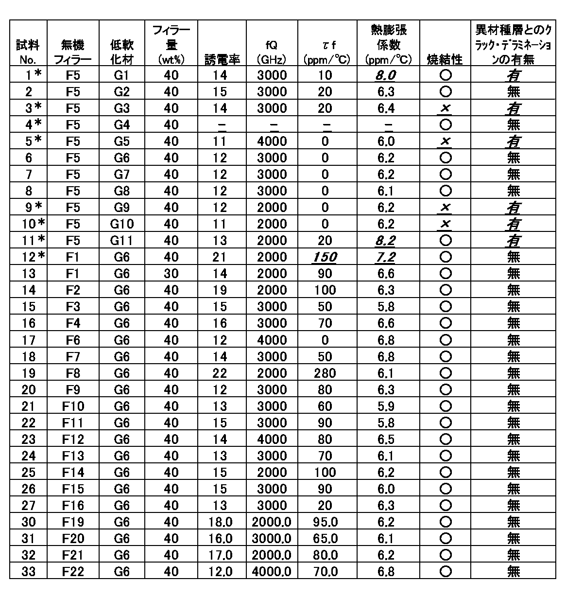

なお、無機フィラー成分で出現した各相(CaTiO3、SrTiO3、Nd2/3TiO3、La2/3TiO3、Sm2/3TiO3、(Mg・Zn)2TiO4は、誘電体磁器組成物中にも残存している。
低温焼結化成分として表1に示すG6を用いた。無機フィラーは表2に示すF2を用いた。
表5は無機フィラー成分の含有量と誘電率、緻密化温度との関係を示すものである。誘電率は無機フィラー成分の混合量の増加により上昇し、40wt%以上で高い誘電率を持つものが製造できる。また、混合量80wt%以下とすることで、緻密化温度が下がり、LTCCでの銀電極焼成温度とほぼ同じ温度とすることができる。混合比は低温焼結化成分:無機フィラーが45~75:25~55であることが好ましく、50~70:30~50であることがさらに好ましい。
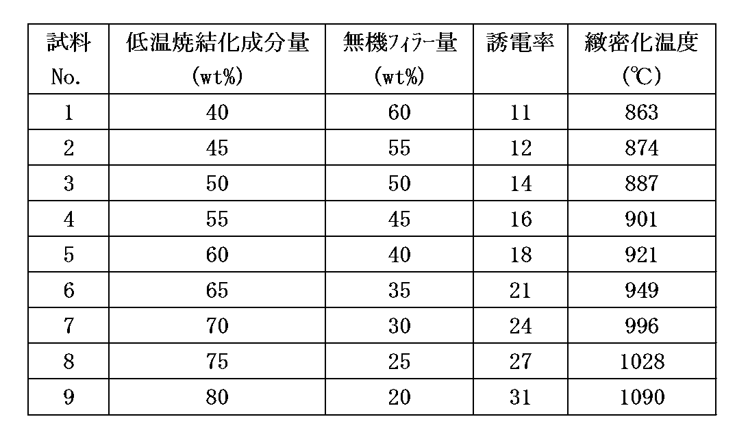
ピーク角度からの分析よりSr長石に加え、SrSiO3、SiO2が析出していることが確認された。これは、Sr長石(SrAl2Si2O8)を形成するためのAl2O3が不足し、余剰のSrO、SiO2がSrSiO3、SiO2となって析出したものと考えられる。SrSiO3の熱膨張係数は10.3ppm/℃であり、同成分の析出は熱膨張係数の増大要因となる。また、SiO2は100℃~200℃付近において相変化による1%程度の異常体積変化を示すことが知られており、熱膨張係数増加への寄与が考えられる。
一方、表1の試料No.G6における低温焼結化成分では、これらのSrSiO3、SiO2が観察されない。低温焼結化成分中のAl2O3を増やしSr長石の析出を促進することで、SrSiO3、SiO2の抑制を行えている。
図4はAl2O3量の低温焼結成分に、高誘電率フィラーを40wt.%混合した誘電体組成物のXRDパターンを示ものである。Sr長石メインピークが最も大きく、32.8°の位置に出ている。なお、図中の□はR(Nd)-M(Mg)-Ti-Si-Oメインピーク2θ=30.2°であり、高誘電率フィラー及び低温焼結成分を個別に焼成した場合には検出されないことから、両者の反応により生じた新規反応生成物であると考えられる。
図5はSr長石メインピークに対するR(Nd)-M(Mg)-Ti-Si-Oメインピークの強度比とAl2O3量の関係を示すものである。なお、R-M-Ti-Si-OメインピークにSr長石ピークと一部重複するため、変動がなくなったところを基準とした。この結果から、Al2O3量増加につれR-M-Ti-Si-Oピーク強度は低下する事が確認された。従って、低温焼結成分でのAl2O3量増量は高誘電率フィラーと低温焼結成分の間の反応を低減する上でも有効であると推測できる。
Mg以外のZn元素でも同様に、Al2O3量が少なければR-M-Ti-Si-O系の相が出る。Nd、La、Sm、Zn量が本発明で規定する範囲を超えて含まれると、この相が出現しやすくなる。出現するメインピークの位置は、上記と同じ2θ=32.8°の位置である。
また、A元素とAl2O3量の関係も同様であり、Al2O3量が少なくA元素量が本発明で規定する範囲を超えて含まれるとA-Ti-Si-O(AはCa、Srのうち少なくとも一種からなる元素)系の相が出現しやすくなる。出現するメインピークの位置は、2θ=29.6°の位置である。
図6は900℃で焼成した混合材の焼結収縮率及び熱膨張係数とAl2O3量の関係を示したものである。
図7は900℃で焼成した混合材の誘電率、τfの関係とAl2O3量の関係を示したものである。
低温焼結成分のAl2O3量増加により混合材の熱膨張係数は低下し、Al2O3量が11.0wt%以上であれば7ppm/℃以下とすることができる。
まず表6に示す組成の誘電体磁器組成物とその他の誘電体層を用いて評価を行なった。

また、その他の誘電体層の仮焼成粉は次のようにして得た。表6の組成の材料をポリエチレン製ボールミルに投入し、更に酸化ジルコニウム製のメディアボールと純水を投入して、20時間湿式混合した。得られたスラリーを加熱乾燥した後、ライカイ機で解砕し、アルミナ製坩堝に入れて、800℃で2時間仮焼成した。得られた仮焼成体を上記ボールミルに投入し、17時間湿式粉砕した後に乾燥し、平均粒径1μmの微粉を得た。
以降の工程は同様にして両者のセラミックグリーンシートが製造される。
スラリーを減圧下で脱泡するとともにエタノールを一部蒸発させ、約7Pa・sの粘度に調整した。スラリーをドクターブレード法によりPET製キャリアフィルム上にシート状に成形し、乾燥して、厚さ0.04mmの基板用グリーンシートを得た。基板用グリーンシートをキャリアフィルムごと180mm角に切断した。
基板用グリーンシートを十分に乾燥した後、Agを主体とする導体ペーストで内部電極パターン及び外部電極パターン4を形成するとともに、該電極パターンを接続するビア電極5を適宜設けた。
このようにして準備した本発明の誘電体組成物を用いたグリーンシート3a、3b、3c及び3dと、その他の誘電体層のグリーンシート2a,2b,2c及び2dを図2に示す形態で配置した。一枚重ねるたびに60℃の温度及び30kg/cm2(2.9MPa)の圧力で仮圧着し、全て積層した後に85℃の温度及び110kg/cm2(10.8MPa)の圧力で熱圧着した。該グリーンシートは、同様の作製方法を用いて得られた、焼結後にAAl2Si2O8相及びAl2O3相を有する誘電体磁器組成物のグリーンシート2a、2b、2c及び2dとともに、図2に示すように、積層、圧着して未焼結多層誘電体基板を得た。
このようにして得られた多層誘電体基板を研磨、観察を行いクラック・デラミネーションの有無を判断した。これらの結果を表3に記載した。なお表4に表3の全ての組成を示す。

本発明の誘電体磁器組成物は、表6に示す組成となるように各原料を混合したものである。また、その他の誘電体層に用いた原料の組成も併記する。
図10は図9の領域Aの四角で囲った部分の拡大図である。(1)部分は無機フィラー成分とほぼ同等の組成であり、(2)部分は低温焼結化成分とほぼ同等の組成である。
図11は、領域Aと領域Bの間の界面を界面垂直方向に向かって測定したSr、Al、Si各元素量のライン分析結果である。誘電体磁器組成物からなる領域Aの層からその他の誘電体層の領域Bに向かうにつれ、境界付近でAl量が急激に増えている。また、図12は同様にして測定したNd、Ti、Caの量を示すものである。Nd、Caはその他の誘電体層側には添加されていない元素である。誘電体磁器組成物の領域ではこれら元素の誘電体磁器組成物全体での平均量にほぼ等しい濃度で検出される。一方、そのほかの誘電体層側ではほぼ検出されなくなる。
この両者での元素が変動している部分が拡散層であり、この拡散層は境界部分において20μm以下の厚みである。拡散層が20μm以下、好ましくは10μm以下であることで無機フィラー成分と低温焼結化成分の特性を併せ持つ優れた多層誘電体基板を得ることができる。
表3、4に示す試料No.2、7、14、15、27の組成になるように原料を調整し、ポリエチレン製ボールミルに投入し、更に酸化ジルコニウム製のメディアボールと純水を投入して、20時間湿式混合した。得られたスラリーを加熱乾燥した後、ライカイ機で解砕し、アルミナ製坩堝に入れて、800℃で2時間仮焼成した。得られた仮焼成体を上記ボールミルに投入し、17時間湿式粉砕した後に乾燥し、平均粒径1μmの微粉を得た。
以降は、低温焼結化成分と無機フィラー成分を互いに仮焼成してから混合粉を得た誘電体磁器組成物と同様にして、焼結体の製造を行なった。
焼結体の誘電率、1GHz~5GHzの周波数範囲における誘電率、1~5GHzにおける品質係数fQ、-20℃~60℃の温度範囲における共振周波数の温度係数τf、40~600℃の温度範囲における熱膨張係数、焼結製、クラック・デラミネーションの有無(高誘電体層の組成は表3、4の試料No.14)を調べた。表8に結果を示す。
品質係数fQ以外は、低温焼結化成分と無機フィラー成分を各々別の温度で仮焼成したものと比較して、ほぼ同等の値が得られる。品質係数fQは若干劣る傾向があるため、高い特性の誘電体磁器組成物、多層誘電体基板を得たければ、低温焼結化成分と無機フィラー成分を各々別の温度で仮焼成する製造方法を適用することが好ましい。
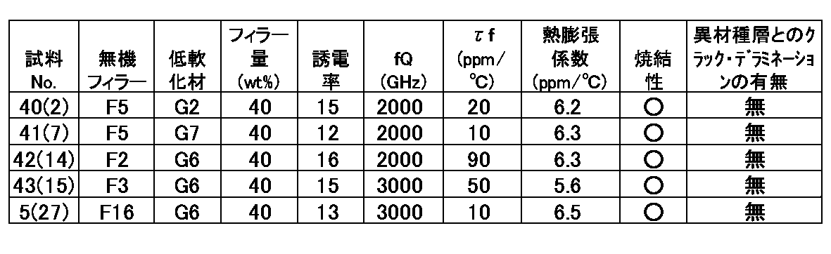
2a~2d グリーンシート
3a~3d グリーンシート
4 電極パターン
5 ビア電極
Claims (18)
- ATiO3(AはCa、Srのうち少なくとも一種からなる元素)相とAAl2Si2O8相を含む誘電体磁器組成物であって、3GHzでの誘電率が10以上、かつ40~600℃の温度範囲における平均熱膨張係数が7ppm/℃未満であることを特徴とする誘電体磁器組成物。
- 主成分であるAl、Si、A、Tiに加えて、添加元素としてBを含み、誘電体磁器組成物全体を100重量部として、Al元素をAl2O3換算で11~25重量%、Si元素をSiO2換算で20~33重量%、A元素をAO換算で5~30重量%、B元素をB2O3換算でAl(Al2O3換算)の0.06倍以上~5重量%、残部としてTiO2(不可避不純物を含む)を含むことを特徴とする、請求項1に記載の誘電体磁器組成物。
- 前記A元素がSrのみの場合は、誘電体磁器組成物全体中のSr元素がSrO換算で5~30重量%であって、前記A元素がCaを含む場合は、誘電体磁器組成物全体中のSr元素がSrO換算で5~15重量%、且つ誘電体磁器組成物全体中のSrとCa元素の総和がAO換算で5~30重量%であることを特徴とする、請求項2に記載の誘電体磁器組成物。
- 誘電体磁器組成物全体を100重量部として、R(RはNd、La、Smのうち少なくとも一種からなる元素)、Mg、Znのうちの少なくとも1種を含むことができ、R2O3換算で0.01~20重量%、MgO換算で0~10重量%、ZnO換算で0~5重量%含有することを特徴とする、請求項2又は3に記載の誘電体磁器組成物。
- Na、K、Cu、Mn、Biのうちの少なくとも1種からなる元素を含み、誘電体磁器組成物全体を100重量部として、Na元素をNa2O換算で0~4重量%、K元素をK2O換算で0~1重量%、Cu元素をCuO換算で0.1~3重量%、Mn元素をMn3O4換算で0.1~3重量%、Bi元素をBi2O3換算で1~5重量%含有することを特徴とする、請求項2乃至4のいずれか一項に記載の誘電体磁器組成物。
- -20℃~60℃の温度範囲における共振周波数の温度係数τfの絶対値が120ppm/℃以下であることを特徴とする請求項5に記載の誘電体磁器組成物。
- 誘電体磁器組成物全体を100重量部として、Agを0.1~3重量%含むことを特徴とする、請求項2乃至6のいずれか一項に記載の誘電体磁器組成物。
- R-M-Ti-Si-O系(RはNd、Sm、Laのうち少なくとも1種からなる元素、MはMg、Znのうち少なくとも1種からなる元素)の相,或いはA-Ti-Si-O系(AはCa、Srのうち少なくとも一種からなる元素)の相が実質的に存在しないことを特徴とする、請求項2乃至7のいずれか一項に記載の誘電体磁器組成物。
- R2/3TiO3(RはNd、La、Smのうち少なくとも一種からなる元素)、及びM2TiO4(MはMg、Znのうち少なくとも一種からなる元素)のうちの少なくとも一種の化合物相を含むことを特徴とする、請求項2乃至8のいずれか一項に記載の誘電体磁器組成物。
- 導体を形成した複数の誘電体層が積層一体化された多層誘電体基板であって、前記複数の誘電体層のうち少なくとも一つの誘電体層が請求項1~9のいずれかに記載の誘電体磁器組成物から構成され、その他の誘電体層がA’Al2Si2O8相(A’はCa、Sr、Baのうち少なくとも一種からなる元素)及びAl2O3相を有する誘電体磁器組成物から構成されることを特徴とする、多層誘電体基板。
- 前記A’Al2Si2O8相及びAl2O3相を有する誘電体層は、主成分であるAl、Si、A’(A’はCa、Sr、Baのうち少なくとも一種からなる元素)、Tiと、副成分として、Bi、Na、K、Coの群のうちの少なくとも1種と、更に、Cu、Mn、Agの群のうちの少なくとも1種とを含むものであって、主成分であるAl、Si、A’、Tiをそれぞれ、誘電体磁器組成物全体を100重量部として、Al2O3換算で10~60重量%、SiO2換算で25~60重量%、A’O換算で7.5~50重量%、TiO2換算で20重量%以下(0を含む)を含み、副成分であるBi、Na、K、Coの群のうちの少なくとも1種をそれぞれ、その主成分100重量部に対して、Bi2O3換算で0~10重量%、Na2O換算で0~5重量%、K2O換算で0~5重量%、CoO換算で0~5重量%を含み、更に、Cu、Mn、Agの群のうちの少なくとも1種を、その主成分100重量部に対して、CuをCuO換算で0~5重量%、MnをMn3O4換算で0~5重量%、Agを0~5重量%で含有することを特徴とする、請求項10に記載の多層誘電体基板。
- 請求項10または請求項11に記載の多層誘電体基板を用いたことを特徴とする電子部品。
- Al、Si、Sr、Ti、Bをそれぞれ必須とし、必要によりNa、K、Cu、Mn、Bi、Agのうち少なくとも一種を含む原料を用意して600℃以上850℃以下で仮焼成することで低温焼結化成分を得る工程と、別途A元素、Tiをそれぞれ必須とし、必要によりNd、La、Sm、Mg、Mnのうち少なくとも一種を含む原料を用意して700℃超1300℃以下で仮焼成することで無機フィラー成分を得る工程と、前記低温焼結化成分と無機フィラー成分を混合した後に低温焼結化成分の仮焼成温度より高く無機フィラー成分の仮焼成温度より低い温度で焼成する工程を有することを特徴とする、請求項1~9のいずれか一項に記載の誘電体磁器組成物の製造方法。
- 前記低温焼結化成分は、少なくともAl、Si、Sr、Bをそれぞれ含み、焼結した場合の組成が、前記低温焼結化成分全体を100重量部として、Al2O3換算で18~40重量%、SiO2換算で40~58重量%、SrO換算で10~40重量%、B2O3換算で1.5~5重量を含む組成となることを特徴とする、請求項13に記載の誘電体磁器組成物の製造方法。
- 前記低温焼結化成分は、Na、K、Cu、Mn、Biの群のうちの少なくとも1種からなる元素を含み、焼結した場合の組成が、前記低温焼結化成分全体を100重量部として、Na2O換算で0~5重量%、K2O換算で0~5重量%、CuO換算で0.01~5重量%、Mn3O4換算で0.01~5重量%、Bi2O3換算で0.1~5重量%含有する組成となることを特徴とする、請求項14に記載の誘電体磁器組成物の製造方法。
- Agを含み、焼結した場合の組成が、前記低温焼結化成分全体を100重量部として、0.5~6重量%含む組成となることを特徴とする、請求項14又は15に記載の誘電体磁器組成物の製造方法。
- 前記無機フィラー成分は、少なくともA(AはCa、Srのうち少なくとも一種からなる元素)とTiをそれぞれ含み、焼結した場合の組成が、前記無機フィラー成分全体を100重量部として、AO換算で10~60重量%、TiO2換算で30~60重量%を含む組成となることを特徴とする、請求項13乃至16のいずれか一項に記載の誘電体磁器組成物の製造方法。
- 前記無機フィラー成分は、R(RはNd、La、Smのうち少なくとも一種からなる元素)、Mg、Znのうちの少なくとも1種を含み、焼結した場合の組成が、前記無機フィラー成分全体を100重量部として、R元素がR2O3換算で0.01~50重量%、Mg元素がMgO換算で0~15重量%、Zn元素がZnO換算で0~10重量%含有する組成となることを特徴とする、請求項17に記載の誘電体磁器組成物の製造方法。
Priority Applications (3)
| Application Number | Priority Date | Filing Date | Title |
|---|---|---|---|
| CN201080013795.XA CN102365249B (zh) | 2009-03-26 | 2010-03-19 | 介电陶瓷组合物、多层介电基板、电子部件和介电陶瓷组合物的制备方法 |
| US13/260,060 US8778819B2 (en) | 2009-03-26 | 2010-03-19 | Dielectric ceramic composition, multilayer dielectric substrate, electronic component, and method for producing dielectric ceramic composition |
| JP2011506023A JP5645136B2 (ja) | 2009-03-26 | 2010-03-19 | 誘電体磁器組成物、多層誘電体基板、電子部品、及び誘電体磁器組成物の製造方法 |
Applications Claiming Priority (2)
| Application Number | Priority Date | Filing Date | Title |
|---|---|---|---|
| JP2009-077027 | 2009-03-26 | ||
| JP2009077027 | 2009-03-26 |
Publications (1)
| Publication Number | Publication Date |
|---|---|
| WO2010110201A1 true WO2010110201A1 (ja) | 2010-09-30 |
Family
ID=42780895
Family Applications (1)
| Application Number | Title | Priority Date | Filing Date |
|---|---|---|---|
| PCT/JP2010/054792 Ceased WO2010110201A1 (ja) | 2009-03-26 | 2010-03-19 | 誘電体磁器組成物、多層誘電体基板、電子部品、及び誘電体磁器組成物の製造方法 |
Country Status (4)
| Country | Link |
|---|---|
| US (1) | US8778819B2 (ja) |
| JP (1) | JP5645136B2 (ja) |
| CN (1) | CN102365249B (ja) |
| WO (1) | WO2010110201A1 (ja) |
Cited By (9)
| Publication number | Priority date | Publication date | Assignee | Title |
|---|---|---|---|---|
| EP2551250A1 (en) * | 2011-07-28 | 2013-01-30 | General Electric Company | Dielectric materials for power tranfer system |
| KR20130052390A (ko) * | 2011-11-11 | 2013-05-22 | 삼성전기주식회사 | 유전체 조성물 및 이를 포함하는 세라믹 전자 부품 |
| US20140057087A1 (en) * | 2011-05-19 | 2014-02-27 | Murata Manufacturing Co., Ltd. | Composite laminate ceramic electronic component |
| KR101532118B1 (ko) * | 2011-12-27 | 2015-06-29 | 삼성전기주식회사 | 유전체 조성물 및 이를 포함하는 세라믹 전자 부품 |
| KR20170020436A (ko) * | 2014-07-09 | 2017-02-22 | 페로 코포레이션 | 미드-k ltcc 조성물 및 디바이스 |
| JP2017171560A (ja) * | 2016-03-25 | 2017-09-28 | 日立金属株式会社 | セラミック基板およびその製造方法 |
| JP2018021914A (ja) * | 2017-08-04 | 2018-02-08 | スリーエム イノベイティブ プロパティズ カンパニー | Icデバイス用ソケット |
| JP2018531857A (ja) * | 2015-07-17 | 2018-11-01 | エプコス アクチエンゲゼルシャフトEpcos Ag | 誘電体組成物、誘電体素子、電子部品および積層電子部品 |
| KR20210121211A (ko) * | 2019-02-27 | 2021-10-07 | 페로 코포레이션 | 높은 q인자를 갖는 ltcc 유전체 조성물 및 장치 |
Families Citing this family (11)
| Publication number | Priority date | Publication date | Assignee | Title |
|---|---|---|---|---|
| EP2551988A3 (en) * | 2011-07-28 | 2013-03-27 | General Electric Company | Dielectric materials for power transfer system |
| JP5821975B2 (ja) * | 2012-02-13 | 2015-11-24 | 株式会社村田製作所 | 複合積層セラミック電子部品 |
| CN103360049B (zh) * | 2012-03-31 | 2016-08-24 | 深圳光启创新技术有限公司 | 一种介质陶瓷 |
| CN103880415B (zh) * | 2014-02-25 | 2015-11-18 | 桂林电子科技大学 | 一种低损耗高介电Sr1-x-y(Ca0.6M0.8/3)y(Na0.5E0.5)xTiO3微波陶瓷及其制备方法 |
| CN109300861B (zh) * | 2018-09-28 | 2021-03-02 | 苏州清陶新能源科技有限公司 | 一种氧化硅基通讯基板及其制备工艺以及应用 |
| CN111384506A (zh) * | 2018-12-31 | 2020-07-07 | 深圳市大富科技股份有限公司 | 一种介质滤波器、制备介质滤波器的方法及通信设备 |
| CN110540420B (zh) * | 2019-10-12 | 2021-09-03 | 无锡鑫圣慧龙纳米陶瓷技术有限公司 | 一种低烧结温度低介微波介质陶瓷及其制备方法 |
| CN113135746B (zh) * | 2020-01-17 | 2022-01-04 | 中国科学院上海硅酸盐研究所 | 一种高绝缘低导热高抗压强度陶瓷材料及其制备方法 |
| CN113072379A (zh) * | 2021-03-31 | 2021-07-06 | 中国振华集团云科电子有限公司 | 一种高介电高机械强度玻璃陶瓷烧结基板及其制备方法 |
| CN112939595B (zh) * | 2021-04-06 | 2022-11-11 | 厦门松元电子股份有限公司 | 高温下近零温度系数的微波介质陶瓷材料及其制备方法 |
| JP7758546B2 (ja) * | 2021-11-22 | 2025-10-22 | Tdk株式会社 | 電子部品 |
Citations (7)
| Publication number | Priority date | Publication date | Assignee | Title |
|---|---|---|---|---|
| JPH0920553A (ja) * | 1995-06-30 | 1997-01-21 | Kyocera Corp | ガラス−セラミック焼結体およびその製造方法 |
| JPH11130533A (ja) * | 1997-10-31 | 1999-05-18 | Kyocera Corp | 配線基板およびその実装構造 |
| JP2002016165A (ja) * | 2000-06-29 | 2002-01-18 | Kyocera Corp | 素子収納用パッケージ |
| JP2002167274A (ja) * | 2000-11-29 | 2002-06-11 | Kyocera Corp | 低温焼結磁器組成物およびそれを用いた多層配線基板 |
| JP2003286074A (ja) * | 2002-01-28 | 2003-10-07 | Kyocera Corp | 誘電体磁器組成物および誘電体磁器 |
| JP2004196652A (ja) * | 2002-12-06 | 2004-07-15 | Hitachi Metals Ltd | 高強度低温焼成セラミック組成物及びその製造方法、並びにこれを用いた積層電子部品 |
| JP2006001755A (ja) * | 2004-06-15 | 2006-01-05 | Hitachi Metals Ltd | 高強度低温焼成セラミック組成物並びにこれを用いた積層電子部品 |
Family Cites Families (5)
| Publication number | Priority date | Publication date | Assignee | Title |
|---|---|---|---|---|
| US6120906A (en) | 1997-03-31 | 2000-09-19 | Kyocera Corporation | Insulated board for a wiring board |
| US6159883A (en) * | 1999-01-07 | 2000-12-12 | Advanced Ceramic X Corp. | Ceramic dielectric compositions |
| KR100539490B1 (ko) | 2002-01-28 | 2005-12-29 | 쿄세라 코포레이션 | 유전체 자기 조성물 및 유전체 자기 |
| WO2004052804A1 (ja) | 2002-12-06 | 2004-06-24 | Hitachi Metals, Ltd. | 高強度低温焼成セラミック組成物及びその製造方法、並びにこれを用いた積層電子部品 |
| JP2005272289A (ja) * | 2003-09-29 | 2005-10-06 | Sanyo Electric Co Ltd | 誘電体磁器組成物及びそれを用いた積層セラミック部品 |
-
2010
- 2010-03-19 US US13/260,060 patent/US8778819B2/en active Active
- 2010-03-19 JP JP2011506023A patent/JP5645136B2/ja active Active
- 2010-03-19 WO PCT/JP2010/054792 patent/WO2010110201A1/ja not_active Ceased
- 2010-03-19 CN CN201080013795.XA patent/CN102365249B/zh active Active
Patent Citations (7)
| Publication number | Priority date | Publication date | Assignee | Title |
|---|---|---|---|---|
| JPH0920553A (ja) * | 1995-06-30 | 1997-01-21 | Kyocera Corp | ガラス−セラミック焼結体およびその製造方法 |
| JPH11130533A (ja) * | 1997-10-31 | 1999-05-18 | Kyocera Corp | 配線基板およびその実装構造 |
| JP2002016165A (ja) * | 2000-06-29 | 2002-01-18 | Kyocera Corp | 素子収納用パッケージ |
| JP2002167274A (ja) * | 2000-11-29 | 2002-06-11 | Kyocera Corp | 低温焼結磁器組成物およびそれを用いた多層配線基板 |
| JP2003286074A (ja) * | 2002-01-28 | 2003-10-07 | Kyocera Corp | 誘電体磁器組成物および誘電体磁器 |
| JP2004196652A (ja) * | 2002-12-06 | 2004-07-15 | Hitachi Metals Ltd | 高強度低温焼成セラミック組成物及びその製造方法、並びにこれを用いた積層電子部品 |
| JP2006001755A (ja) * | 2004-06-15 | 2006-01-05 | Hitachi Metals Ltd | 高強度低温焼成セラミック組成物並びにこれを用いた積層電子部品 |
Cited By (17)
| Publication number | Priority date | Publication date | Assignee | Title |
|---|---|---|---|---|
| US20140057087A1 (en) * | 2011-05-19 | 2014-02-27 | Murata Manufacturing Co., Ltd. | Composite laminate ceramic electronic component |
| US9067380B2 (en) * | 2011-05-19 | 2015-06-30 | Murata Manufacturing Co., Ltd. | Composite laminate ceramic electronic component |
| US9881732B2 (en) | 2011-07-28 | 2018-01-30 | General Electric Company | Dielectric materials for power transfer system |
| EP2551250A1 (en) * | 2011-07-28 | 2013-01-30 | General Electric Company | Dielectric materials for power tranfer system |
| KR20130052390A (ko) * | 2011-11-11 | 2013-05-22 | 삼성전기주식회사 | 유전체 조성물 및 이를 포함하는 세라믹 전자 부품 |
| US9076578B2 (en) | 2011-11-11 | 2015-07-07 | Samsung Electro-Mechanics Co., Ltd. | Dielectric composition and ceramic electronic component including the same |
| KR101588916B1 (ko) * | 2011-11-11 | 2016-01-27 | 삼성전기주식회사 | 유전체 조성물 및 이를 포함하는 세라믹 전자 부품 |
| KR101532118B1 (ko) * | 2011-12-27 | 2015-06-29 | 삼성전기주식회사 | 유전체 조성물 및 이를 포함하는 세라믹 전자 부품 |
| KR101931108B1 (ko) * | 2014-07-09 | 2018-12-20 | 페로 코포레이션 | 미드-k ltcc 조성물 및 디바이스 |
| KR20170020436A (ko) * | 2014-07-09 | 2017-02-22 | 페로 코포레이션 | 미드-k ltcc 조성물 및 디바이스 |
| JP2018531857A (ja) * | 2015-07-17 | 2018-11-01 | エプコス アクチエンゲゼルシャフトEpcos Ag | 誘電体組成物、誘電体素子、電子部品および積層電子部品 |
| US10490350B2 (en) | 2015-07-17 | 2019-11-26 | Tdk Electronics Ag | Dielectric composition, dielectric element, electronic component and multi-layer electronic component |
| JP2017171560A (ja) * | 2016-03-25 | 2017-09-28 | 日立金属株式会社 | セラミック基板およびその製造方法 |
| US10383220B2 (en) | 2016-03-25 | 2019-08-13 | Hitachi Metals, Ltd. | Ceramic substrate and method for production thereof |
| JP2018021914A (ja) * | 2017-08-04 | 2018-02-08 | スリーエム イノベイティブ プロパティズ カンパニー | Icデバイス用ソケット |
| KR20210121211A (ko) * | 2019-02-27 | 2021-10-07 | 페로 코포레이션 | 높은 q인자를 갖는 ltcc 유전체 조성물 및 장치 |
| KR102640378B1 (ko) | 2019-02-27 | 2024-02-23 | 페로 코포레이션 | 높은 q인자를 갖는 ltcc 유전체 조성물 및 장치 |
Also Published As
| Publication number | Publication date |
|---|---|
| US20120015198A1 (en) | 2012-01-19 |
| JPWO2010110201A1 (ja) | 2012-09-27 |
| CN102365249A (zh) | 2012-02-29 |
| JP5645136B2 (ja) | 2014-12-24 |
| CN102365249B (zh) | 2014-06-04 |
| US8778819B2 (en) | 2014-07-15 |
Similar Documents
| Publication | Publication Date | Title |
|---|---|---|
| JP5645136B2 (ja) | 誘電体磁器組成物、多層誘電体基板、電子部品、及び誘電体磁器組成物の製造方法 | |
| JP4883228B2 (ja) | 低温焼結セラミック焼結体および多層セラミック基板 | |
| CN101836518B (zh) | 陶瓷多层基板 | |
| KR101290089B1 (ko) | 저온 소결 세라믹 재료 및 세라믹 기판 | |
| CN108605417A (zh) | 陶瓷基板及其制造方法 | |
| WO2012157299A1 (ja) | ガラスセラミック組成物 | |
| US7446067B2 (en) | Ceramic green sheet and ceramic substrate | |
| JP2001114554A (ja) | 低温焼成セラミック組成物及びセラミック多層基板 | |
| JP6728859B2 (ja) | セラミック基板およびその製造方法 | |
| EP1640350B1 (en) | Composition for ceramic substrate, ceramic substrate, process for producing ceramic substrate and glass composition | |
| EP1568668B1 (en) | Ceramic composition being fired at low temperature and having high strength and method for preparing the same, and laminated electronic parts using the same | |
| US8231961B2 (en) | Low temperature co-fired ceramic material, low temperature co-fired ceramic body, and multilayer ceramic substrate | |
| US7211533B2 (en) | Oxide porcelain composition, ceramic multilayer substrate, and ceramic electronic component | |
| US8652982B2 (en) | Ceramic sintered body and method for producing ceramic sintered body | |
| JP4587758B2 (ja) | ガラスセラミック基板 | |
| JP4496529B2 (ja) | 多層セラミック基板の製造方法及び多層セラミック基板 | |
| JP2007250728A (ja) | セラミック積層デバイスおよびその製造方法 | |
| JP4514301B2 (ja) | 多層配線基板の製造方法 | |
| JP4129384B2 (ja) | 誘電体磁器およびそれを用いた多層配線基板 | |
| JP4174668B2 (ja) | 誘電体磁器組成物、並びにその製造方法、それを用いた誘電体磁器及び積層セラミック部品 | |
| JP2004253757A (ja) | 積層セラミック電子部品およびその製造方法 | |
| JP2003026472A (ja) | 積層セラミック電子部品の製造方法、積層セラミック電子部品および積層セラミック電子部品製造用の生の複合積層体 | |
| JP2004203645A (ja) | 低温焼成磁器および電子部品 | |
| JP2012240890A (ja) | セラミックス組成物、セラミックス焼結体及び電子部品 |
Legal Events
| Date | Code | Title | Description |
|---|---|---|---|
| WWE | Wipo information: entry into national phase |
Ref document number: 201080013795.X Country of ref document: CN |
|
| 121 | Ep: the epo has been informed by wipo that ep was designated in this application |
Ref document number: 10755998 Country of ref document: EP Kind code of ref document: A1 |
|
| ENP | Entry into the national phase |
Ref document number: 2011506023 Country of ref document: JP Kind code of ref document: A |
|
| WWE | Wipo information: entry into national phase |
Ref document number: 13260060 Country of ref document: US |
|
| NENP | Non-entry into the national phase |
Ref country code: DE |
|
| 122 | Ep: pct application non-entry in european phase |
Ref document number: 10755998 Country of ref document: EP Kind code of ref document: A1 |