WO2010103967A1 - 有機エレクトロニクス素子及びその製造方法 - Google Patents
有機エレクトロニクス素子及びその製造方法 Download PDFInfo
- Publication number
- WO2010103967A1 WO2010103967A1 PCT/JP2010/053411 JP2010053411W WO2010103967A1 WO 2010103967 A1 WO2010103967 A1 WO 2010103967A1 JP 2010053411 W JP2010053411 W JP 2010053411W WO 2010103967 A1 WO2010103967 A1 WO 2010103967A1
- Authority
- WO
- WIPO (PCT)
- Prior art keywords
- organic
- layer
- base material
- electrode
- light emitting
- Prior art date
- Legal status (The legal status is an assumption and is not a legal conclusion. Google has not performed a legal analysis and makes no representation as to the accuracy of the status listed.)
- Ceased
Links
Images



Classifications
-
- H—ELECTRICITY
- H10—SEMICONDUCTOR DEVICES; ELECTRIC SOLID-STATE DEVICES NOT OTHERWISE PROVIDED FOR
- H10K—ORGANIC ELECTRIC SOLID-STATE DEVICES
- H10K77/00—Constructional details of devices covered by this subclass and not covered by groups H10K10/80, H10K30/80, H10K50/80 or H10K59/80
- H10K77/10—Substrates, e.g. flexible substrates
- H10K77/111—Flexible substrates
-
- H—ELECTRICITY
- H10—SEMICONDUCTOR DEVICES; ELECTRIC SOLID-STATE DEVICES NOT OTHERWISE PROVIDED FOR
- H10K—ORGANIC ELECTRIC SOLID-STATE DEVICES
- H10K50/00—Organic light-emitting devices
- H10K50/80—Constructional details
- H10K50/84—Passivation; Containers; Encapsulations
- H10K50/844—Encapsulations
- H10K50/8445—Encapsulations multilayered coatings having a repetitive structure, e.g. having multiple organic-inorganic bilayers
-
- H—ELECTRICITY
- H10—SEMICONDUCTOR DEVICES; ELECTRIC SOLID-STATE DEVICES NOT OTHERWISE PROVIDED FOR
- H10K—ORGANIC ELECTRIC SOLID-STATE DEVICES
- H10K85/00—Organic materials used in the body or electrodes of devices covered by this subclass
- H10K85/30—Coordination compounds
- H10K85/341—Transition metal complexes, e.g. Ru(II)polypyridine complexes
-
- H—ELECTRICITY
- H10—SEMICONDUCTOR DEVICES; ELECTRIC SOLID-STATE DEVICES NOT OTHERWISE PROVIDED FOR
- H10K—ORGANIC ELECTRIC SOLID-STATE DEVICES
- H10K85/00—Organic materials used in the body or electrodes of devices covered by this subclass
- H10K85/30—Coordination compounds
- H10K85/341—Transition metal complexes, e.g. Ru(II)polypyridine complexes
- H10K85/342—Transition metal complexes, e.g. Ru(II)polypyridine complexes comprising iridium
-
- H—ELECTRICITY
- H10—SEMICONDUCTOR DEVICES; ELECTRIC SOLID-STATE DEVICES NOT OTHERWISE PROVIDED FOR
- H10K—ORGANIC ELECTRIC SOLID-STATE DEVICES
- H10K85/00—Organic materials used in the body or electrodes of devices covered by this subclass
- H10K85/30—Coordination compounds
- H10K85/341—Transition metal complexes, e.g. Ru(II)polypyridine complexes
- H10K85/346—Transition metal complexes, e.g. Ru(II)polypyridine complexes comprising platinum
-
- H—ELECTRICITY
- H10—SEMICONDUCTOR DEVICES; ELECTRIC SOLID-STATE DEVICES NOT OTHERWISE PROVIDED FOR
- H10K—ORGANIC ELECTRIC SOLID-STATE DEVICES
- H10K85/00—Organic materials used in the body or electrodes of devices covered by this subclass
- H10K85/30—Coordination compounds
- H10K85/341—Transition metal complexes, e.g. Ru(II)polypyridine complexes
- H10K85/348—Transition metal complexes, e.g. Ru(II)polypyridine complexes comprising osmium
-
- H—ELECTRICITY
- H10—SEMICONDUCTOR DEVICES; ELECTRIC SOLID-STATE DEVICES NOT OTHERWISE PROVIDED FOR
- H10K—ORGANIC ELECTRIC SOLID-STATE DEVICES
- H10K85/00—Organic materials used in the body or electrodes of devices covered by this subclass
- H10K85/60—Organic compounds having low molecular weight
- H10K85/631—Amine compounds having at least two aryl rest on at least one amine-nitrogen atom, e.g. triphenylamine
-
- Y—GENERAL TAGGING OF NEW TECHNOLOGICAL DEVELOPMENTS; GENERAL TAGGING OF CROSS-SECTIONAL TECHNOLOGIES SPANNING OVER SEVERAL SECTIONS OF THE IPC; TECHNICAL SUBJECTS COVERED BY FORMER USPC CROSS-REFERENCE ART COLLECTIONS [XRACs] AND DIGESTS
- Y02—TECHNOLOGIES OR APPLICATIONS FOR MITIGATION OR ADAPTATION AGAINST CLIMATE CHANGE
- Y02E—REDUCTION OF GREENHOUSE GAS [GHG] EMISSIONS, RELATED TO ENERGY GENERATION, TRANSMISSION OR DISTRIBUTION
- Y02E10/00—Energy generation through renewable energy sources
- Y02E10/50—Photovoltaic [PV] energy
- Y02E10/549—Organic PV cells
-
- Y—GENERAL TAGGING OF NEW TECHNOLOGICAL DEVELOPMENTS; GENERAL TAGGING OF CROSS-SECTIONAL TECHNOLOGIES SPANNING OVER SEVERAL SECTIONS OF THE IPC; TECHNICAL SUBJECTS COVERED BY FORMER USPC CROSS-REFERENCE ART COLLECTIONS [XRACs] AND DIGESTS
- Y02—TECHNOLOGIES OR APPLICATIONS FOR MITIGATION OR ADAPTATION AGAINST CLIMATE CHANGE
- Y02P—CLIMATE CHANGE MITIGATION TECHNOLOGIES IN THE PRODUCTION OR PROCESSING OF GOODS
- Y02P70/00—Climate change mitigation technologies in the production process for final industrial or consumer products
- Y02P70/50—Manufacturing or production processes characterised by the final manufactured product
Definitions
- the present invention relates to a method for manufacturing an organic electronics element and an organic electronics element manufactured by the manufacturing method.
- the manufacturing method of the organic electronics element utilized as a surface light source, a display, a solar cell, etc., especially the manufacturing method of the organic electronics element provided on flexible base materials, such as a plastic film, and a manufacturing method
- the present invention relates to an organic electronic device.
- an organic layer of an organic electronics element also referred to as an organic compound layer, a hole injection layer, a hole transport layer, a light emitting layer, a hole blocking layer, an electron transport layer, a hole transport layer, and the like
- Various methods such as vapor deposition, sputtering, CVD, PVD, and solvent coating can be used. Among these methods, the manufacturing process can be simplified, the manufacturing cost can be reduced, the workability can be improved, It is known that a wet film-forming method such as a coating method is advantageous from the viewpoint of application to a flexible large-area element such as a light or an illumination light source.
- Patent Document 1 describe an organic electroluminescence element (hereinafter, also referred to as an organic EL element) that is expected to be used as a solid light-emitting large-area full-color display element or a writing light source array.
- a method of manufacturing by a roll-to-roll method which is regarded as an inexpensive manufacturing method, has been studied.
- organic light emission is made of a polymer material such as polystyrene, polymethyl methacrylate, polyvinyl carbazole or the like in which a low-molecular luminescent dye is dispersed or dissolved, or a polymer material such as a polyphenylene vinylene derivative or a polyalkylfluorene derivative.
- a method of winding production by a coating method using a solvent is known (for example, see Patent Document 1).
- organic EL materials include low molecular weight materials and high molecular weight materials.
- Low-molecular materials can be purified by sublimation, easy to purify, and high-purity organic EL materials can be used.
- polymer materials are highly pure. Refining is difficult, and there is a demerit that performance such as efficiency and lifetime deteriorates. Recently, a wet film forming method using a low molecular material has been studied.
- the present invention has been made in view of the above problems, and an object of the present invention is to provide a method for manufacturing an organic electronic device having low manufacturing cost and excellent performance stability.
- An object of the present invention is to provide a method for producing an organic electroluminescence element which is less likely to have a lifetime deterioration or a reduction in light emitting area due to a decrease in gas barrier properties of generation or sealing.
- An organic electronics structure having a first electrode, at least one organic layer and a second electrode is formed on a flexible substrate, and then a flexible sealing substrate is formed on the organic electronics structure.
- the temperature of the said heat processing is less than Tg (glass transition point) of the said base material, and is more than Tg (glass transition point) of the said sealing base material.
- the present invention it is possible to provide a method for manufacturing an organic electronic device that is low in manufacturing cost and excellent in performance stability.
- a method for manufacturing an organic electroluminescence element that is low in manufacturing cost, has little lifetime deterioration due to generation of light emission unevenness and a decrease in sealing gas barrier property, and a decrease in light emission area.
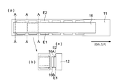
- (A) is a schematic diagram which shows the fundamental structure of the whole organic EL element
- (b) is a schematic diagram which shows the structure of the organic EL structure part of an organic EL element. It is a conceptual diagram of the process which shows the sealing process and cutting position which adhere
- Organic EL elements one of the organic electronics elements, are extremely sensitive to substances such as water and oxygen that interfere with the electrochemical processes leading to light emission by forming excitons in the light-emitting layer. It is. When these substances diffuse from the outside, the light emission efficiency and the driving life are remarkably shortened, and it becomes impossible to obtain practical illumination and display performance. In addition, water, oxygen, and the like may change the electrical and chemical characteristics of the electrode surface and the inside, thereby obstructing the movement of electrons and holes. As a result, the practical characteristics are greatly deteriorated.
- the organic EL element is encapsulated with a desiccant and enclosed in a structure sealed with glass or a metal can, or a sealing substrate having a barrier performance against gas components such as moisture and oxygen is used. Ensuring performance is being studied.
- the present inventors have studied in detail the heat treatment (heating adhesion) when sealing the organic EL element with a thermosetting adhesive using the sealing substrate.
- the element may have a reduced lifetime or reduced luminous efficiency. It has been found that these problems can be solved by heat treatment at a temperature equal to or higher than Tg.
- the sealing substrate is heat-treated at a temperature lower than Tg, the sealing substrate is hard, so that the organic EL structure to be bonded is damaged by the pressure in the bonding step, and the sealing group Since the material does not follow the shape of the organic EL structure, the adhesion is lowered and the gas barrier property is lowered. As a result, it is presumed that the device has deteriorated the lifetime or the light emission efficiency.
- the sealing substrate when the sealing substrate is heat-treated at a temperature equal to or higher than Tg, the sealing substrate softens and follows the shape of the organic EL structure to be bonded thereto, so that the organic EL structure is damaged. It is difficult to solve problems such as deterioration of lifetime and decrease in luminous efficiency.
- the method for producing an organic electronic device of the present invention can be suitably used particularly as a method for producing an organic EL device.
- the organic EL device produced by the method for producing an organic electronic device of the present invention has improved gas barrier properties and is excellent in performance such as half life and luminous efficiency.
- an organic electronics structure having a first electrode, at least one organic layer, and a second electrode is formed on a flexible substrate, and then the organic electronics structure is formed.
- the temperature of the said heat processing is less than Tg (glass transition point) of the said base material, and the said sealing base material It is characterized by a temperature equal to or higher than the Tg (glass transition point).
- ⁇ Washing process> A process of cleaning the substrate by a process that combines wet cleaning, such as rolling out the substrate wound in a roll and immersing it in an ultrasonic cleaning tank, and dry cleaning such as plasma cleaning. It is.
- An organic EL structure composed of electrodes, various organic layers, etc. on a substrate by a well-known technique such as vapor deposition, spin coating, extrusion coating, ink jet, or printing. It is a process of forming.
- an organic EL structure having a first electrode, at least one organic layer, and a second electrode is formed on a flexible substrate.
- FIG. 1 shows a basic configuration of an organic EL element which is one of organic electronic elements.
- the electrode is not shown.
- FIG. 1A is a schematic diagram showing the overall configuration of the organic EL element.
- the organic EL element 1 has a configuration in which the organic EL structure 2 on the substrate 12 is sealed with a sealing substrate layer 16 including an adhesive 16A and a sealing substrate (sealing film) 16B.
- FIG. 1B is a schematic diagram showing the configuration of the organic EL structure 2 portion of the organic EL element.
- ⁇ Substrate supply step> A step of feeding and supplying the roll-shaped substrate 11 provided with the organic EL structure 2.
- ⁇ Sealing step> A long sealing base material 16B is adhered to the base material 11 with a thermosetting adhesive 16A so as to cover the organic EL structure 2, thereby forming the sealing base material layer 16. It is a sealing process. Details of the sealing substrate 16B and the thermosetting adhesive 16A will be described later.
- a flexible sealing base material is bonded only to the center part excluding the electrode lead part of the organic EL structure on the organic EL structure, and less than Tg of the base material. And it heat-processes at the temperature more than Tg of the said sealing base material.
- thermosetting adhesive 16A After bonding the sealing substrate 16B, the thermosetting adhesive 16A is cured, and then the substrate 11 provided with the organic EL structure 2 and the sealing substrate layer 16 is cut. This is a cutting process for forming an organic EL element.
- FIG. 2A shows a sealing process in which a sealing substrate is bonded to a substrate provided with an organic EL structure with a thermosetting adhesive, and cutting after the thermosetting adhesive is cured. It is a conceptual diagram of a process.
- FIG. 2B is a cut one organic EL element
- FIG. 2C is a side view of FIG.
- the above-described means makes the organic EL structure less susceptible to damage, and solves problems such as uneven light emission, deterioration of lifetime, and decrease in light emission efficiency.
- Base material As a base material which concerns on this invention, it is required to use the flexible base material which can give flexibility (flexibility) to an organic EL element, for example, a resin film. However, metal, glass, quartz, or the like can be partially used as the base material depending on the purpose. As the substrate, a long substrate is preferable from the viewpoint of productivity.
- polyesters such as polyethylene terephthalate (PET) and polyethylene naphthalate (PEN), polyethylene, polypropylene, cellophane, cellulose diacetate, cellulose triacetate, cellulose acetate butyrate, cellulose acetate propionate (CAP), Cellulose esters such as cellulose acetate phthalate and cellulose nitrate or their derivatives, polyvinylidene chloride, polyvinyl alcohol, polyethylene vinyl alcohol, syndiotactic polystyrene, polycarbonate, norbornene resin, polymethylpentene, polyether ketone, polyimide, polyether Sulfone (PES), polyphenylene sulfide, polysulfones, polyester Cycloolefin resins such as terimide, polyether ketone imide, polyamide, fluororesin, nylon, polymethyl methacrylate, acrylic or polyarylate, Arton (trade name, manufactured by JSR) or Apel (trade name
- the thickness of the substrate cannot be generally specified, but is preferably 3 to 400 ⁇ m, more preferably 50 to 300 ⁇ m, and still more preferably 100 to 200 ⁇ m.
- the types and Tg of the resin film preferably used as the base material according to the present invention are as follows.
- the resin film includes nylon (Ny), nylon (KNy) coated with vinylidene chloride (PVDC), polypropylene coated with PVDC (KOP), cellophane coated with PVDC (KPT), and polyethylene-vinyl alcohol.
- a polymer (eval) can be used.
- the Tg of the multilayer film is defined as the Tg of the resin having the lowest Tg among the constituent resins.
- a barrier film may be formed on the surface of the resin film, and the gas barrier property of the barrier film has a water vapor permeability (40 ° C., 90% RH) of 0 measured by a method according to JIS K 7129-1992. It is preferable that the film has a barrier property of 0.01 g / (m 2 ⁇ day ⁇ atm) or less, and the oxygen permeability (20 ° C., 100% RH) measured by a method in accordance with JIS K 7126-1992 is 10 ⁇ 3 g / (m 2 ⁇ day) or less and a water vapor transmission rate of 10 ⁇ 3 g / (m 2 ⁇ day) or less is preferable, and the water vapor transmission rate and the oxygen transmission rate are preferably Is more preferably 10 ⁇ 5 g / (m 2 ⁇ day) or less.
- the material for forming the barrier film may be any material that has a function of suppressing the intrusion of elements that cause deterioration of elements such as moisture and oxygen.
- silicon oxide, silicon dioxide, silicon nitride, or the like can be used.
- the method for forming the barrier film is not particularly limited.
- vacuum deposition, sputtering, reactive sputtering, molecular beam epitaxy, cluster ion beam, ion plating, plasma polymerization, atmospheric pressure plasma polymerization A plasma CVD method, a laser CVD method, a thermal CVD method, a coating method, or the like can be used, but an atmospheric pressure plasma polymerization method as described in JP-A-2004-68143 is particularly preferable.
- the organic EL element according to the present invention has at least a first electrode and a second electrode. Usually, one is an anode and the other is a cathode. The preferred anode and cathode configurations are described below.
- an electrode material made of a metal, an alloy, an electrically conductive compound, or a mixture thereof having a high work function (4 eV or more) is preferably used.
- electrode substances include metals such as Au, and conductive light-transmitting materials such as CuI, indium tin oxide (ITO), SnO 2 , and ZnO.
- a material such as IDIXO (In 2 O 3 —ZnO) that can form an amorphous light-transmitting conductive film may be used.
- these electrode materials may be formed into a thin film by a method such as vapor deposition or sputtering, and a pattern having a desired shape may be formed by a photolithography method, or when the pattern accuracy is not required (about 100 ⁇ m or more) ), A pattern may be formed through a mask having a desired shape when the electrode material is deposited or sputtered. Or when using the substance which can be apply
- the sheet resistance as the anode is preferably several hundred ⁇ / ⁇ or less. Further, although the film thickness depends on the material, it is usually selected in the range of 10 to 1000 nm, preferably 10 to 200 nm.
- cathode a material having a low work function (4 eV or less) metal (referred to as an electron injecting metal), an alloy, an electrically conductive compound, and a mixture thereof as an electrode material is used.
- electrode materials include aluminum, sodium, sodium-potassium alloy, magnesium, lithium, magnesium / copper mixture, magnesium / silver mixture, magnesium / aluminum mixture, magnesium / indium mixture, aluminum / aluminum oxide (Al 2 O 3 ) mixtures, indium, lithium / aluminum mixtures, rare earth metals and the like.
- the cathode can be produced by forming a thin film of these electrode materials by a method such as vapor deposition or sputtering.
- the sheet resistance as the cathode is preferably several hundred ⁇ / ⁇ or less, and the film thickness is usually selected in the range of 10 nm to 5 ⁇ m, preferably 50 to 200 nm.
- either the anode or the cathode of the organic EL element is configured to be light transmissive.
- the light emitting layer according to the present invention is a layer that emits light by recombination of electrons and holes injected from the electrode, the electron transport layer, or the hole transport layer, and the light emitting portion is in the layer of the light emitting layer. May be the interface between the light emitting layer and the adjacent layer.
- the structure of the light emitting layer according to the present invention is not particularly limited as long as the light emitting material included satisfies the above requirements.
- the total thickness of the light emitting layers is preferably in the range of 1 to 200 nm, and more preferably 5 to 100 nm because a lower driving voltage can be obtained.
- a light-emitting material or a host compound which will be described later, is formed by forming a film by a known thinning method such as a vacuum deposition method, a spin coating method, an extrusion coating method, an inkjet method, or a printing method. Can do.
- a plurality of light emitting materials may be mixed in each light emitting layer, or a phosphorescent light emitting material and a fluorescent light emitting material may be mixed and used in the same light emitting layer. Further, the light emitting layer may be formed from a plurality of layers.
- the light emitting layer preferably contains a host compound and a light emitting material (also referred to as a light emitting dopant compound) and emits light from the light emitting material.
- a light emitting material also referred to as a light emitting dopant compound
- a compound having a phosphorescence quantum yield of phosphorescence emission at room temperature (25 ° C.) of less than 0.1 is preferable. More preferably, the phosphorescence quantum yield is less than 0.01. Moreover, it is preferable that the volume ratio in the layer is 50% or more among the compounds contained in a light emitting layer.
- known host compounds may be used alone or in combination of two or more.
- the organic EL element can be made highly efficient.
- the host compound used in the present invention may be a conventionally known low molecular compound or a high molecular compound having a repeating unit, and a low molecular compound having a polymerizable group such as a vinyl group or an epoxy group (evaporation polymerizable light emitting host). )But it is good.
- the known host compound a compound that has a hole transport ability and an electron transport ability, prevents the emission of light from being long-wavelength, and has a high Tg (glass transition point) is preferable.
- the glass transition point (Tg) is a value determined by a method based on JIS-K-7121 using DSC (Differential Scanning Colorimetry).
- a fluorescent compound or a phosphorescent material (also referred to as a phosphorescent compound or a phosphorescent compound) is used.
- a phosphorescent material is a compound in which light emission from an excited triplet is observed. Specifically, it is a compound that emits phosphorescence at room temperature (25 ° C.), and the phosphorescence quantum yield is 0 at 25 ° C. A preferred phosphorescence quantum yield is 0.1 or more, although it is defined as 0.01 or more compounds.
- the phosphorescent quantum yield can be measured by the method described in Spectra II, page 398 (1992 version, Maruzen) of Experimental Chemistry Lecture 4 of the 4th edition.
- the phosphorescence quantum yield in a solution can be measured using various solvents.
- the phosphorescence quantum yield (0.01 or more) is achieved in any solvent. Just do it.
- the carrier recombination occurs on the host compound to which the carrier is transported to generate an excited state of the host compound, and this energy is transferred to the phosphorescent material.
- Energy transfer type to obtain light emission from the phosphorescent light emitting material, and another one is that the phosphorescent light emitting material becomes a carrier trap, and recombination of carriers occurs on the phosphorescent light emitting material, and light emission from the phosphorescent light emitting material is obtained.
- the excited state energy of the phosphorescent material is required to be lower than the excited state energy of the host compound.
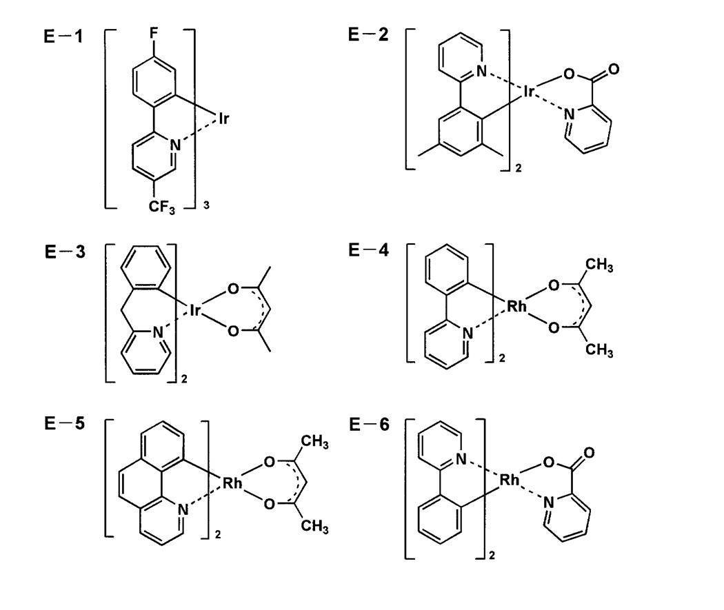
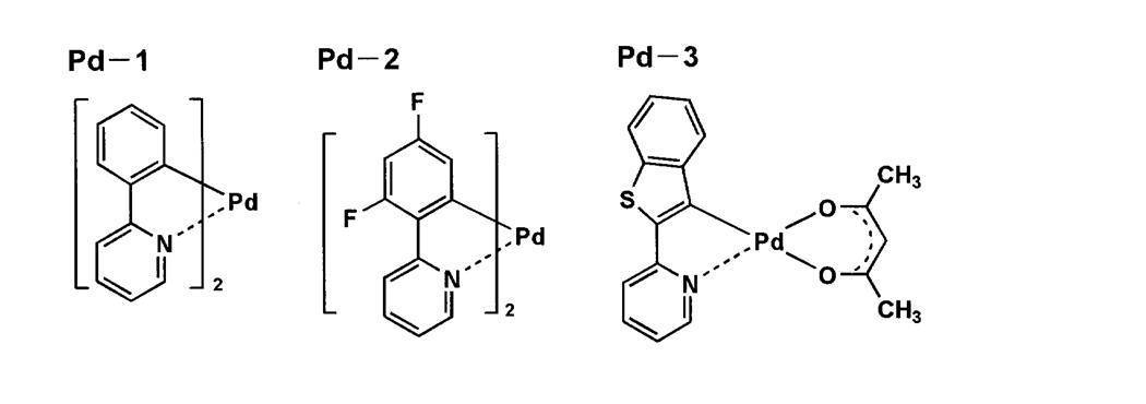
- the phosphorescent light-emitting material can be appropriately selected from known materials used for the light-emitting layer of the organic EL element, and is preferably a complex compound containing a group 8-10 metal in the periodic table of elements. More preferably, an iridium compound, an osmium compound, a platinum compound (platinum complex compound), or a rare earth complex, and most preferably an iridium compound.
- Fluorescent light emitters can also be used in the organic EL device according to the present invention.
- fluorescent emitters include coumarin dyes, pyran dyes, cyanine dyes, croconium dyes, squalium dyes, oxobenzanthracene dyes, fluorescein dyes, rhodamine dyes, pyrylium dyes. Examples thereof include dyes, perylene dyes, stilbene dyes, polythiophene dyes, and rare earth complex phosphors.
- At least one light emitting layer may contain two or more kinds of light emitting materials, and the concentration ratio of the light emitting materials in the light emitting layer may vary in the thickness direction of the light emitting layer.
- injection layer electron injection layer, hole injection layer
- the injection layer is provided as necessary, and there are an electron injection layer and a hole injection layer, and as described above, it exists between the anode and the light emitting layer or the hole transport layer and between the cathode and the light emitting layer or the electron transport layer. May be.
- An injection layer is a layer provided between an electrode and an organic layer in order to reduce drive voltage and improve light emission luminance.
- Organic EL element and its forefront of industrialization (issued by NTT Corporation on November 30, 1998) 2), Chapter 2, “Electrode Materials” (pages 123 to 166) in detail, and includes a hole injection layer (anode buffer layer) and an electron injection layer (cathode buffer layer).
- anode buffer layer hole injection layer
- copper phthalocyanine is used.
- examples thereof include a phthalocyanine buffer layer represented by an oxide, an oxide buffer layer represented by vanadium oxide, an amorphous carbon buffer layer, and a polymer buffer layer using a conductive polymer such as polyaniline (emeraldine) or polythiophene.
- cathode buffer layer (electron injection layer) The details of the cathode buffer layer (electron injection layer) are described in JP-A-6-325871, JP-A-9-17574, JP-A-10-74586, and the like. Specifically, strontium, aluminum, etc.
- Metal buffer layer typified by lithium, alkali metal compound buffer layer typified by lithium fluoride, alkaline earth metal compound buffer layer typified by magnesium fluoride, oxide buffer layer typified by aluminum oxide, etc.
- the buffer layer (injection layer) is preferably an extremely thin film, and the film thickness is preferably in the range of 0.1 nm to 5 ⁇ m although it depends on the material.
- the blocking layer is provided as necessary in addition to the basic constituent layer of the organic compound thin film as described above. For example, it is described in JP-A Nos. 11-204258 and 11-204359, and “Organic EL elements and the forefront of industrialization (published by NTT Corporation on November 30, 1998)” on page 237. There is a hole blocking (hole blocking) layer.
- the hole blocking layer has a function of an electron transport layer and is composed of a hole blocking material having a function of transporting electrons and having a remarkably small ability to transport holes, while transporting electrons. By blocking holes, the recombination probability of electrons and holes can be improved. Moreover, the structure of the electron carrying layer mentioned later can be used as a hole-blocking layer concerning this invention as needed.
- the hole blocking layer is preferably provided adjacent to the light emitting layer.
- the electron blocking layer in a broad sense, has a function of a hole transport layer, and is made of a material having a function of transporting holes while having a remarkably small ability to transport electrons, while transporting holes. By blocking electrons, the probability of recombination of electrons and holes can be improved. Moreover, the structure of the positive hole transport layer mentioned later can be used as an electron blocking layer as needed.
- the film thickness of the hole blocking layer and the electron transport layer according to the present invention is preferably 3 to 100 nm, more preferably 5 to 30 nm.
- the hole transport layer is made of a hole transport material having a function of transporting holes, and in a broad sense, a hole injection layer and an electron blocking layer are also included in the hole transport layer.
- the hole transport layer can be provided as a single layer or a plurality of layers.
- the hole transport material has either hole injection or transport or electron barrier properties, and may be either organic or inorganic.
- triazole derivatives oxadiazole derivatives, imidazole derivatives, polyarylalkane derivatives, pyrazoline derivatives and pyrazolone derivatives, phenylenediamine derivatives, arylamine derivatives, amino-substituted chalcone derivatives, oxazole derivatives, styrylanthracene derivatives, fluorenone derivatives, hydrazone derivatives
- Examples thereof include stilbene derivatives, silazane derivatives, aniline copolymers, and conductive polymer oligomers, particularly thiophene oligomers.
- the above-mentioned materials can be used as the hole transport material, but it is preferable to use a porphyrin compound, an aromatic tertiary amine compound and a styrylamine compound, particularly an aromatic tertiary amine compound.
- aromatic tertiary amine compounds and styrylamine compounds include N, N, N ′, N′-tetraphenyl-4,4′-diaminophenyl; N, N′-diphenyl-N, N′— Bis (3-methylphenyl)-[1,1′-biphenyl] -4,4′-diamine (TPD); 2,2-bis (4-di-p-tolylaminophenyl) propane; 1,1-bis (4-di-p-tolylaminophenyl) cyclohexane; N, N, N ′, N′-tetra-p-tolyl-4,4′-diaminobiphenyl; 1,1-bis (4-di-p-tolyl) Aminophenyl) -4-phenylcyclohexane; bis (4-dimethylamino-2-methylphenyl) phenylmethane; bis (4-di-p-tolylaminoph
- a polymer material in which these materials are introduced into a polymer chain or these materials are used as a polymer main chain can also be used.
- inorganic compounds such as p-type-Si and p-type-SiC can also be used as the hole injection material and the hole transport material.
- JP-A-11-251067, J. Org. Huang et. al. A so-called p-type hole transport material described in a book (Applied Physics Letters 80 (2002), p. 139) can also be used. In the present invention, it is preferable to use these materials because a light-emitting element with higher efficiency can be obtained.
- the hole transport layer can be formed by thinning the hole transport material by a known method such as a vacuum deposition method, a spin coating method, an extrusion coating method, an ink jet method, or a printing method.
- the thickness of the hole transport layer is not particularly limited, but is usually about 5 nm to 5 ⁇ m, preferably 5 to 200 nm.
- the hole transport layer may have a single layer structure composed of one or more of the above materials.
- a hole transport layer having a high p property doped with impurities examples thereof include JP-A-4-297076, JP-A-2000-196140, 2001-102175, J.A. Appl. Phys. 95, 5773 (2004), and the like.
- a hole transport layer having such a high p property because a device with lower power consumption can be produced.
- the electron transport layer is made of a material having a function of transporting electrons, and in a broad sense, an electron injection layer and a hole blocking layer are also included in the electron transport layer.
- the electron transport layer can be provided as a single layer or a plurality of layers.
- an electron transport material also serving as a hole blocking material used for an electron transport layer adjacent to the light emitting layer on the cathode side is injected from the cathode.
- any material can be selected and used from among conventionally known compounds. For example, nitro-substituted fluorene derivatives, diphenylquinone derivatives Thiopyrandioxide derivatives, carbodiimides, fluorenylidenemethane derivatives, anthraquinodimethane and anthrone derivatives, oxadiazole derivatives and the like.
- a thiadiazole derivative in which the oxygen atom of the oxadiazole ring is substituted with a sulfur atom, or a quinoxaline derivative having a quinoxaline ring known as an electron withdrawing group can also be used as an electron transport material.
- a polymer material in which these materials are introduced into a polymer chain or these materials are used as a polymer main chain can also be used.
- metal complexes of 8-quinolinol derivatives such as tris (8-quinolinol) aluminum (Alq 3 ), tris (5,7-dichloro-8-quinolinol) aluminum, tris (5,7-dibromo-8-quinolinol) Aluminum, tris (2-methyl-8-quinolinol) aluminum, tris (5-methyl-8-quinolinol) aluminum, bis (8-quinolinol) zinc (Znq), etc.
- Mg Metal complexes replaced with Cu, Ca, Sn, Ga, or Pb can also be used as electron transport materials.
- metal-free or metal phthalocyanine or those having terminal ends substituted with an alkyl group or a sulfonic acid group can be preferably used as the electron transporting material.
- the distyrylpyrazine derivatives exemplified as the material of the light emitting layer can also be used as the electron transport material, and inorganic semiconductors such as n-type-Si and n-type-SiC can be used as well as the hole injection layer and the hole transport layer. It can be used as an electron transport material.
- the electron transport layer can be formed by thinning the electron transport material by a known method such as a vacuum deposition method, a spin coating method, an extrusion coating method, an ink jet method, or a printing method.
- the thickness of the electron transport layer is not particularly limited, but is usually about 5 nm to 5 ⁇ m, preferably 5 to 200 nm.
- the electron transport layer may have a single layer structure composed of one or more of the above materials.
- an electron transport layer having a high n property doped with impurities examples thereof include JP-A-4-297076, JP-A-10-270172, JP-A-2000-196140, 2001-102175, J.A. Appl. Phys. 95, 5773 (2004), and the like.
- an electron transport layer having such a high n property because an element with lower power consumption can be produced.
- Method for producing organic EL structure As an example of a method for producing an organic EL structure according to the present invention, a method for producing an organic EL structure comprising an anode / hole injection layer / hole transport layer / light emitting layer / hole blocking layer / electron transport layer / cathode. explain.
- a thin film made of a desired electrode material for example, an anode material
- a suitable support substrate by a method such as vapor deposition or sputtering so as to have a film thickness of 1 ⁇ m or less, preferably 10 to 200 nm, thereby producing an anode.
- vacuum deposition method spin coating method, extrusion coating method, ink jet method, printing method, etc. as methods for thinning this organic compound thin film, but it is easy to obtain a uniform film and pinholes are generated.
- the vacuum evaporation method, the extrusion coating method, the ink jet method, and the printing method are particularly preferable. Further, a different film forming method may be applied for each layer.
- a thin film made of a cathode material is formed thereon by a method such as vapor deposition or sputtering so as to have a film thickness of 1 ⁇ m or less, preferably in the range of 50 to 200 nm, and a cathode is provided.
- the organic EL structure is preferably manufactured from the hole injection layer to the cathode consistently by a single evacuation, but may be taken out halfway and subjected to different film forming methods. At that time, it is necessary to consider that the work is performed in a dry inert gas atmosphere.
- the flexible structure is formed on the organic EL structure.
- the sealing base material is bonded and heat-treated at a temperature lower than Tg (glass transition point) of the base material and equal to or higher than Tg (glass transition point) of the sealing base material described below.
- the difference in Tg between the base material and the sealing base material is preferably 30 to 50 ° C.
- the preferred base material-sealing base combinations are stretched PEN-stretched PET, stretched PEN-unstretched PET, unstretched PEN-unstretched PET, stretched PEN-unstretched PET.
- the temperature of the heat treatment is preferably less than Tg of the base material and above Tg of the sealing base material, and the absolute value is preferably 100 to 140 ° C.
- the organic EL element can be sealed by covering the cathode surface with the sealing substrate in an environment purged with an inert gas.
- an inert gas a rare gas such as He or Ar is preferably used in addition to N 2 , and the ratio of the inert gas in the gas is preferably 90 to 99.9% by volume. Preservability is improved by sealing in an environment purged with an inert gas.
- the sealing substrate according to the present invention is for sealing an organic EL element and protecting the element from a severe external environment such as temperature change, humidity, oxygen, and impact.
- the resin film described in the above substrate can be used as the sealing substrate.
- the types and Tg of the resin film preferably used in the present invention are as follows.
- the resin film includes nylon (Ny), nylon (KNy) coated with vinylidene chloride (PVDC), polypropylene coated with PVDC (KOP), cellophane coated with PVDC (KPT), and polyethylene-vinyl alcohol.
- a polymer (eval) can be used.
- Tg of the sealing base material of a multilayer film is defined as Tg of resin with the lowest Tg among the resin to comprise.
- the thickness of the sealing substrate cannot be generally specified, but is preferably 3 to 400 ⁇ m, more preferably 5 to 200 ⁇ m, and even more preferably 10 to 100 ⁇ m.
- a barrier film is formed on the sealing substrate.
- the barrier film include a metal vapor deposition film, a metal foil, and an inorganic vapor deposition film.
- a metal foil in which the barrier film easily follows the shape of the sealing substrate at the time of bonding is preferable.
- the thickness of the barrier film is preferably several ⁇ m to 50 ⁇ m depending on the material.
- metal used for a metal vapor deposition film or a metal foil there is no particular limitation on the type of metal, for example, copper (Cu), aluminum (Al), gold (Au), brass, nickel (Ni), titanium (Ti), Examples include copper alloy, stainless steel, tin (Sn), and high nickel alloy.
- aluminum is particularly preferable from the viewpoint of barrier properties (moisture permeability, oxygen permeability) and cost.
- the inorganic film for example, silicon oxide, silicon dioxide, silicon nitride or the like can be used. Furthermore, in order to improve the brittleness of the film, it is more preferable to have a laminated structure of these inorganic layers and layers made of organic materials. Although there is no restriction
- the gas barrier properties of the sealing substrate are preferably those having an oxygen permeability of 10 ⁇ 3 g / (m 2 ⁇ day) or less and a water vapor permeability of 10 ⁇ 3 g / (m 2 ⁇ day) or less. Further, it is more preferable that both the water vapor permeability and the oxygen permeability are 10 ⁇ 5 g / (m 2 ⁇ day) or less.
- thermosetting adhesive having a reactive vinyl group such as an acrylic acid oligomer or a methacrylic acid oligomer.
- a thermosetting adhesive having a reactive vinyl group such as an acrylic acid oligomer or a methacrylic acid oligomer.
- ThreeBond 1152, 1153 and the like can be used.
- thermosetting adhesive that cures within 1 hour at a temperature equal to or higher than the Tg of the sealing base and lower than the Tg of the base is preferable.
- stretched polyethylene naphthalate Tg, 155 ° C.
- stretched polyethylene terephthalate Tg, 110 ° C.
- An adhesive is mentioned.
- the electrode and the organic layer are covered outside the electrode on the side facing the support substrate with the organic layer interposed therebetween, and inorganic and organic layers are formed in contact with the support substrate.
- a sealing film can also be suitably used.
- the material for forming the film may be any material that has a function of suppressing entry of elements that cause deterioration of elements such as moisture and oxygen.
- silicon oxide, silicon dioxide, silicon nitride, or the like may be used. it can.
- vacuum deposition method sputtering method, reactive sputtering method, molecular beam epitaxy method, cluster ion beam method, ion plating method, plasma polymerization method, atmospheric pressure plasma
- a polymerization method a plasma CVD method, a laser CVD method, a thermal CVD method, a coating method, or the like can be used.
- FIG. 3 is a schematic diagram of a manufacturing apparatus and a manufacturing process for producing an organic EL structure having a multilayer structure using a base material.
- a gas barrier layer As an example of an organic EL element, a gas barrier layer, a first electrode, a hole transport layer, a light emitting layer, an electron injection layer, a second electrode, The case of the organic EL element formed in the order of the sealing layers is performed.
- the first electrode forming step is omitted.
- the manufacturing process includes a substrate supply step 3 ′, a hole transport layer formation step 4 ′ for forming a hole transport layer, a light emitting layer formation step 5 ′ for forming a light emitting layer, and a first recovery step 6 ′.
- the supply step 3 'to the light emitting layer forming step 5' are continuously performed under atmospheric pressure conditions, and after winding up under atmospheric pressure conditions, the electron injection layer forming step 7 '
- the case where the process up to the sealing layer forming step 9 ′ is continuously performed under reduced pressure is shown.
- the second recovery step 10 ' may be arranged under either atmospheric pressure conditions or reduced pressure conditions.
- the supply process 3 ′ includes a feeding process 301 ′ and a surface treatment process 302 ′.
- a base material 301′b base material in which a gas barrier film used to form at least one organic EL element and at least one anode layer including the first electrode are already formed in this order.
- A) is wound around the core and supplied in a roll state.
- 301'a shows the former winding roll of base material 301'b.
- the surface treatment step 302 ' includes a cleaning surface modification apparatus 302'a and first antistatic means 302'b.
- the cleaning surface modification apparatus 302′a cleans and modifies the surface of the first electrode (not shown) of the substrate A sent from the feeding step 301 ′ before applying the hole transport layer forming coating solution. Therefore, for example, it is preferable to use a low-pressure mercury lamp, an excimer lamp, a plasma cleaning apparatus, or the like.
- a cleaning surface modification treatment is performed by irradiating a low-pressure mercury lamp with a wavelength of 184.2 nm at an irradiation intensity of 5 to 20 mW / cm 2 and a distance of 5 to 15 mm. Conditions are mentioned.
- atmospheric pressure plasma is preferably used as the condition for the cleaning surface modification treatment by the plasma cleaning apparatus.
- the cleaning conditions include a condition in which a cleaning surface modification treatment is performed using a gas containing 1 to 5% by volume of oxygen in argon gas, a frequency of 100 kHz to 150 MHz, a voltage of 10 V to 10 kV, and an irradiation distance of 5 to 20 mm.
- the first antistatic means 302'b has a non-contact type static elimination preventing device 302'b1 and a contact type static elimination preventing device 302'b2.
- the non-contact type static elimination preventing device 302′b1 include a non-contact type ionizer, and the type of ionizer is not particularly limited, and the ion generation method may be either an AC method or a DC method.
- An AC type, a double DC type, a pulsed AC type, and a soft X-ray type can be used, but the AC type is particularly preferable from the viewpoint of precise static elimination.
- Air or N 2 is used as the injection gas required when using the AC type, but it is preferable to use N 2 with sufficiently high purity.
- it is selected from a blower type or a gun type.
- a static elimination roll or a conductive brush connected to the ground is used as the contact type static elimination preventing device 302'b2.
- the static elimination roll as the static eliminator is grounded and removes the surface charge by rotatingly contacting the neutralized surface.
- a static elimination roll in addition to rolls made of metal such as aluminum, copper, nickel, and stainless steel, rolls made of elastic plastic or rubber mixed with conductive materials such as carbon black, metal powder, and metal fibers are used. used. In particular, an elastic material is preferable in order to improve contact with the belt-like flexible continuous sheet.
- the conductive brush connected to the earth include a neutralizing bar or a neutralizing yarn structure having a brush member made of conductive fibers arranged linearly or a linear metal brush.
- the neutralization bar is not particularly limited, but a corona discharge type is preferably used.
- SJ-B manufactured by Keyence Corporation is used.
- the static elimination yarn is not particularly limited, but usually a flexible yarn-like yarn can be preferably used.
- the non-contact type antistatic device 302'b1 is used on the first electrode surface side of the flexible base material A, and the contact type antistatic device 302'b2 is used on the back surface side of the flexible base material A.
- the first antistatic means removes the charge of the base material and prevents the adhesion of the dust and the dielectric breakdown, thereby improving the yield of the elements.
- the hole transport layer forming step 4 ′ includes a backup roll 401 ′ that holds the substrate A, and a part of the base A that is held by the backup roll 401 ′ that serves as an external extraction electrode.
- the solvent of the coating film a ′ for forming the hole transport layer formed on the first electrode (not shown) on the substrate A is removed by removing the wet coater 402 ′ to be applied and removing the hole transport layer b ′.
- It has a drying device 403 ′ having a drying air supply port 403′a, an exhaust port 403′b, and a transport roll 403′c. Note that the drying device 403 includes a portion that enables heat treatment.
- the second static elimination processing unit 404 ′ represents a second charge removal processing means for removing charge from the formed hole transport layer b ′.
- the second static elimination processing unit 404 ′ includes the same non-contact type static elimination prevention device 404′a and the contact type static elimination prevention device 404′b2 as the first static elimination processing unit 302′b.
- the light emitting layer forming step 5 ' includes a first coating step 5'a, a first drying step 5'b, a second coating step 5'c, a second drying step 5'd, and a third coating step 5'e. And a third drying step 5'f.
- the first application step 5'a includes an electrostatic nozzle ejection device 5'a1, a holding base 5a2, and a first accumulator portion 5'a3 as first droplet ejection means.
- the application by the electrostatic nozzle discharge device 5'a1 is such that the liquid droplets discharged from the electrostatic nozzle discharge device 5'a1 land on the hole transport layer at regular intervals and emit light discontinuously.
- a layer forming coating film c ′ (discontinuous second organic functional layer forming coating film) is formed.
- the electrostatic nozzle ejection device was used as the coating means, but other existing coating devices (for example, continuous coating with an extrusion coating device and formation of a discontinuous coating film by wiping and removing part of the coating film with a wiping device) ) But that's fine
- the first accumulator unit 5′a3 moves the roll 5′a31 in the vertical direction (in the direction of the arrow in the drawing), so that the transport speed between the hole transport layer forming step 4 ′ and the first coating step 5′a is increased.
- the roll 5'a31 can be added according to the speed difference.
- the first drying step 5'b includes a drying device 5'b1 having a drying air supply port 5'b11, an exhaust port 5'b12, and a transport roll 5'b13, and formation of the formed discontinuous light emitting layer.
- 3rd static elimination process means 5'b2 which neutralizes static electricity coating film c '.
- the third static elimination processing means 5'b2 has the same non-contact type static elimination prevention device 5'b21 and contact type static elimination prevention device 5'b22 as the first static elimination processing means 302'b.
- the drying device 5'b1 has a portion that allows heat treatment inside.
- the discontinuous light emitting layer forming coating c ′ (discontinuous second organic functional layer forming coating) is removed by the drying device 5′b1 and the discontinuous light emitting layer d ′ (discontinuous second organic) is removed. Functional layer).
- the second coating step 5'c has an electrostatic nozzle ejection device 5'c1, a mounting table 5'c2, and a second accumulator portion 5'c3 as second droplet ejection means.
- the liquid droplets discharged from the electrostatic nozzle discharge device 5'c1 are discontinuous formed in the first application step 5'a. Landing on an uncoated portion of the light emitting layer d ′ (discontinuous second organic functional layer) forms a continuous light emitting layer forming coating film e ′ (continuous second organic functional layer forming coating film).
- the electrostatic nozzle ejection device was used as the coating means, but other existing coating devices (for example, continuous coating with an extrusion coating device and formation of a discontinuous coating film by wiping and removing part of the coating film with a wiping device) ) But it doesn't matter.
- the second accumulator unit 5′c3 moves the roll 5′c31 in the vertical direction (in the direction of the arrow in the drawing), so that the conveyance speed of the first application step 5′a and the second application step 5′c is increased.
- the roll 5'c31 can be added according to the speed difference.
- the second drying step 5'd includes a drying device 5'd1 having a drying air supply port 5'd11, an exhaust port 5'd12, and a transporting roll 5'd13, and the formed continuous light emitting layer f '.
- 4th static elimination process means 5'd2 which performs static elimination of this.
- the fourth static elimination processing means 5'd2 has the same non-contact type static elimination prevention device 5'd21 and contact type static elimination prevention device 5'd22 as the first static elimination processing means 302'b.
- the drying device 5'd1 has a portion that enables heat treatment inside.
- the third coating step 5'e includes an electrostatic nozzle discharge device 5'e1, a mounting table 5'e2, and a third accumulator unit 5'e3 as third droplet discharge means.
- the third accumulator unit 5′e3 moves the roll 5′e31 in the vertical direction (in the direction of the arrow in the drawing), so that the conveyance speed between the second application step 5′c and the third application step 5′e is increased.
- the roll 5'e31 can be added according to the speed difference.
- the electrostatic nozzle discharge device 5'e1 is applied to form droplets discharged from the electrostatic nozzle discharge device 5'e1 using the same solvent as the light emitting layer forming coating solution.
- the electrostatic nozzle ejection device 5'a1, the electrostatic nozzle ejection device 5'c1 and the electrostatic nozzle ejection device 5'e1 are arranged in a frame of the device (not shown) so that the substrate can be moved in the width direction. It is preferable to arrange in.
- the electrostatic nozzle ejection device was used as the coating means, but other existing coating devices (for example, continuous coating with an extrusion coating device and formation of a discontinuous coating film by wiping and removing part of the coating film with a wiping device) ) But that's fine
- the third drying step 5'f includes a drying device 5'f1 having a drying air supply port 5'f11, an exhaust port 5'f12, and a conveying roll 5'f13, and a continuous light emitting layer h 'formed.
- 4th static elimination process means 5'f2 which performs static elimination of this.
- the fourth static elimination processing means 5'f2 has the same non-contact type static elimination prevention device 5'f21 and contact type static elimination prevention device 5'f22 as the first static elimination processing means 302'b.
- the drying device 5'f1 has a portion that allows heat treatment inside.
- the continuous light emitting layer f ′ (continuous second organic functional layer) is removed before being removed by the drying device 5′f1. Is dissolved to uniformize the continuous light emitting layer f ′ (continuous second organic functional layer) and level the surface, thereby forming a uniform continuous light emitting layer h ′.
- the first recovery step 6 ' has a fourth accumulator portion 6'a and a winding device (not shown).
- the base material (referred to as base material B) on which the continuous light emitting layer h ′ is formed is wound around a winding core and collected by a roll base material B 601 ′.
- the fourth accumulator section 6'a and the roll 6'a1 move in the vertical direction (in the direction of the arrow in the figure), so that the conveying speed of the third coating step 5'e and the winding speed of the first recovery step 6 'are obtained.
- the roll 6'a1 can be added according to the speed difference.
- the electron injection layer forming step 7 ′ includes a supply unit 701 ′ and an electron injection layer formation unit 702 ′.
- the supply unit 701 ′ the roll-shaped substrate B 601 ′ produced in the previous process is fed out and supplied to the electron injection layer forming unit 702 ′.
- the electron injection layer forming part 702 ′ the electron injection layer i ′ is formed on the continuous light emitting layer h ′.
- 702'a represents a vapor deposition apparatus, and 702'b represents an evaporation source container.
- the flexible base material on which the electron injection layer i ′ is formed is subsequently sent to the second electrode forming step 8 ′.
- the second electrode j ′ is formed on the electron injection layer i ′ formed by the electron injection layer formation unit 702 ′ in the second electrode formation unit 801 ′.
- Reference numeral 801'a denotes a vapor deposition apparatus, and 801'b denotes an evaporation source container.
- the flexible base material on which the second electrode j ′ is formed is subsequently sent to the protective layer forming step 9 ′.
- the protective layer forming step 9 ′ includes a fifth accumulator unit 901 ′, a protective layer forming device 902 ′, and a fifth antistatic means 903 ′.
- the fifth antistatic means 903 ' has the same non-contact type static elimination preventing apparatus 903'a and the contact type static elimination preventing apparatus 903'b as the first static elimination processing means 302'b.
- the protective layer k ′ is formed on the second electrode j ′ by the protective layer forming apparatus 902 ′ except for the end portion of the second electrode j ′ formed in the second electrode forming step 8, so that at least on the substrate.
- One organic EL element is produced.
- the collection step 10 ′ has a winding device (not shown).
- a flexible base material on which at least one organic EL element is formed (referred to as a flexible base material C) is placed on the protective layer k ′ side inside by a winding device (not shown). It is wound up and collected.
- Reference numeral 10'a denotes a roll-like base material in which a flexible base material C is wound around a winding core and collected as a roll shape.
- the oxygen concentration is 1 to 100 ppm and the water concentration is 1 to 100 ppm. It is preferable to store in the environment.
- coating is performed by the electrostatic nozzle ejection device 5'a1, in the second coating process 5'c, coating by the electrostatic nozzle ejection device 5'c1 and third coating process 5'e.
- the application by the electrostatic nozzle ejection device 5'e1 is a method of moving the electrostatic nozzle ejection device 5a1, the electrostatic nozzle ejection device 5c1 and the electrostatic nozzle ejection device 5e1 in the width direction of the base material in accordance with the transport speed of the base material. Is mentioned.
- the electron injection layer forming step 7 'and the second electrode forming step 8' are shown in the case of the vapor deposition apparatus.
- the electron injection layer and the second electrode are formed by electron injection independent of the vapor deposition method.
- a method of forming the layer and the second electrode can also be used.
- the system which sticks a sealing film instead of the sealing layer shown to this figure may be sufficient.
- the hole transport layer forming coating solution and the light emitting layer forming coating solution used in the production process shown in FIG. 5 have at least one organic compound material and at least one solvent.
- the surface tension is preferably 15 ⁇ 10 ⁇ 3 to 55 ⁇ 10 ⁇ 3 N / m.
- FIG. 4 is a schematic diagram illustrating an example of the sealing substrate layer forming process 140 and the cutting process 150.
- the sealing base material layer forming process 140 includes a bonding process 142 and a curing process 143.
- the sealing base material layer 16 made of the sealing member 16B is formed on the organic EL structure by pressure-bonding the sealing base material 16B having the adhesive layer 16A to the base material 11 with a roller.
- thermosetting adhesive that is cured by heating by an epoxy-based, acrylic-based, acrylic urethane-based heating means, or an ultraviolet curable adhesive that is cured by ultraviolet irradiation of an ultraviolet irradiation means.
- a thermosetting adhesive is preferably used.
- the adhesive layer 16A is cured by heating with the heating means 143A, and the sealing layer 16 is fixed to the upper surface of the organic EL structure.
- the adhesive is of a type using ultraviolet curing, it is cured by irradiating with UV light.
- the curing step 143 may be before the cutting step or after the cutting step, but is preferably after the cutting step in terms of manufacturing efficiency.
- the cutting step 150 is a step of obtaining each organic EL element by cutting the base material on which the sealing base material layer 16 is formed at a predetermined position.
- the cutting step 150 includes a cutting unit 151A, and the long substrate 11 on which the organic EL structure and the sealing base material layer are formed is cut by the cutting unit 151A in the cutting step 150 to obtain an organic EL element.
- the obtained organic EL element has the 1st electrode, the positive hole transport layer, the organic light emitting layer, the 2nd electrode layer, the electron injection layer, and the sealing base material layer on the base material.
- the cutting means 151A may be a guillotine cutter that moves up and down, or a circular rotary cutter that suppresses vibration.
- the cutting position is performed along a cutting line A that cuts in the width direction shown in FIG.
- the distance between the cutting line A and the lead portion of the first electrode and the second electrode is preferably 1 mm or more from the viewpoints of gas barrier properties of the adhesive layer and prevention of electrode short-circuiting.
- Each organic EL element is cut along the cutting line.
- a base material (Example 1 of Japanese Patent Application Laid-Open No. 2007-83644) in which a barrier film is formed on a polyethylene naphthalate film (Teijin-DuPont film, hereinafter abbreviated as PEN) having a thickness of 100 ⁇ m, a width of 200 mm, and a length of 500 m Formed by the method described in 1).
- PEN polyethylene naphthalate film
- an alignment mark is provided on the base material in advance to indicate the position where the first electrode is formed, and ITO (indium tin oxide) having a thickness of 120 nm under a vacuum environment condition of 5 ⁇ 10 ⁇ 1 Pa is formed by sputtering.
- Mask pattern film formation was performed, and 12 rows of first electrodes each having a size of 10 mm ⁇ 10 mm having lead portions on both ends in the width direction of the substrate were continuously formed and wound at regular intervals.
- First hole transport layer formation A solution obtained by diluting polyethylene dioxythiophene / polystyrene sulfonate (PEDOT / PSS, Baytron P AI 4083 manufactured by Bayer) with pure water at 65% and methanol at 5% by mass is used as a coating solution for forming the first hole transport layer. It apply
- PEDOT / PSS polystyrene sulfonate
- Coating conditions for the first hole transport layer forming coating solution are as follows: temperature is 25 ° C., dew point temperature is ⁇ 20 ° C. or less in an N 2 gas environment at atmospheric pressure, and cleanliness class 5 or less (JIS B 9920). I went there.
- the substrate on which the first hole transport layer is formed is irradiated with microwaves (2.45 GHz) to detect the position of the first electrode as a thermal pattern, and this is used as a positioning mark.
- Methyl ethyl ketone which is a good solvent that swells the hole transport layer, is supplied to unnecessary portions on the extraction electrode portion and around the first electrode, and the internal temperature of the device is 10 ° C. by the wiping device of FIG. By rubbing with a pressure of about 1.96 ⁇ 10 5 Pa so that the relative speed of the wiping head (pressing roll and tape-like member) with the base material is 5 cm / second, the organic electronics structure is continuously wiped. Removed.
- the temperature is 5 ° C.
- the vapor pressure of methyl ethyl ketone is 4173 Pa at 5 ° C.
- the microwave irradiator was a ⁇ -reactor manufactured by Shikoku Keiki Kogyo Co., Ltd.
- the substrate was dried and wound up.
- the solvent was supplied at a rate of 10 ml / min and a temperature of 10 ° C.
- the second hole transport layer, the organic light emitting layer, and the electron transport layer were sequentially formed by repeating coating, drying, and winding using an extrusion coater.
- the conveyance speed was 3 m / min.
- a toluene solution containing 1% by mass and 0.1% by mass of PVK and dopant 4 was formed on the second hole transport layer by extrusion coating. It dried at 120 degreeC and was set as the light emitting layer with a film thickness of about 50 nm.
- Electrode transport layer A 1-butanol solution containing 0.5% by mass of the electron transport material 1 was similarly formed on the light emitting layer by extrusion coating. It dried at 60 degreeC and was set as the electron carrying layer with a film thickness of about 15 nm.
- the coating conditions were as follows: N 2 gas environment having a temperature of 25 ° C., a dew point temperature of ⁇ 20 ° C. or lower, atmospheric pressure, and a cleanliness class of 5 or lower (JIS B 9920).
- Organic layer patterning removal step 2 Supplying the wound base material on which the first hole transport layer is formed, positioning the first electrode pattern formed on the base material as a positioning mark using a microwave sensor, By using the wiping device shown in FIG. 7, unnecessary portions on the extraction electrode portion of one electrode and around the first electrode are o-xylene, an electron having a high affinity for the second hole transport layer and the light emitting layer.
- a solvent in which 1-butanol, which is a good solvent, is mixed at a mixing ratio of 2: 1 is supplied to the transport layer, the temperature is 15 ° C., and the relative speed of the pressing roll (tape-like member) with the base material is the same as described above.
- the pressing force of the wiping head was 1.96 ⁇ 10 5 Pa.
- the inside of the wiping device was cooled to 15 ° C., and the total supply amount of the solvent was 20 ml / min.
- the vapor pressure of 1-butanol at 15 ° C. is 368 Pa
- the vapor pressure of o-xylene at 15 ° C. is 475 Pa.
- the three organic layers thus swollen or dissolved were rubbed at once to perform removal patterning. After patterning, the film was dried with a drying apparatus and temporarily wound up and stored for 1 hour.
- a cathode buffer layer (electron injection layer), a second electrode, and a sealing layer are sequentially formed on the organic layer under the conditions shown below, and cut and further heat-treated to produce an organic EL panel. It was set to 1.
- cathode buffer layer (electron injection layer)
- a portion of the electron transport layer and the portion excluding the lead-out portion of the first electrode is 5 ⁇ 10 ⁇ 4 Pa by a vapor deposition apparatus.
- a mask pattern deposition film was formed, and a cathode buffer layer (electron injection layer) having a thickness of 0.5 nm was laminated.
- a film obtained by laminating PET 50 ⁇ m as a sealing member and aluminum foil 30 ⁇ m as a barrier film was used using the apparatus shown in FIG.
- thermosetting adhesive with a melting point of 120 ° C. was used as the adhesive for the adhesive layer, and the layer thickness was 30 ⁇ m.
- thermosetting After pasting the sealing substrate, thermosetting was performed at 100 ° C. for 1 hour.
- an organic EL element 1 was obtained by detecting an alignment mark in the size of each organic EL element, and cutting the substrate having a plurality of organic EL structures produced according to the position of the alignment mark.
- Organic EL elements 2 to 15 were prepared in the same manner as in the preparation of the organic EL element 1, except that the base resin, the sealing base resin, and the heat treatment temperature after bonding were changed as shown in Table 1.
- Light emission unevenness Using a source measure unit type 2400 manufactured by KEITHLEY, a direct current voltage was applied to the organic EL element to emit light at 200 cd / cm 2 . Light emission unevenness was observed with a 50 ⁇ microscope and evaluated according to the following criteria.
- A There is no light emission unevenness.
- ⁇ There is a slight light emission unevenness that does not cause a problem in practice.
- X There is a light emission unevenness that causes a problem in practice where the uniform light emission part is less than 70% (light emission area (barrier property)).
- the organic EL device according to the present invention has little emission unevenness and a high emission ratio.
- the organic EL element of the comparative example has a low light emission ratio because the sealing performance is reduced due to the influence of internal stress, light is not emitted from the end, and dark spots (non-light emitting points) are increased or grown. It is thought that it was reduced.
- Example 2 In the production of the organic EL element 2 of Example 1, after forming the hole injection layer, the following power generation layer coating solution was applied, dried at 120 ° C., and a raw web having a dried thickness of 150 nm was produced. Except for the above, an organic photoelectric conversion element having a desiccant in the element was prepared in the same manner as the preparation of the organic EL element 2.
- Power generation layer coating solution 6 ml of chlorobenzene, regioregular P3HT (poly-3-hexylthiophene) having a number average molecular weight of 45000 and fullerene derivative PCBM (6,6-phenyl-C61-butyric acid methyl ester) at a mass ratio of 1: 1 and 3% A solution dissolved so as to be% was used. After film formation, the film was dried under a nitrogen stream while slowly transporting through a 140 ° C. drying zone to form a power generation layer having a dry film thickness of 150 nm.
- the organic photoelectric conversion device having the obtained desiccant in the device was evaluated for short-circuit current density Jsc when the solar simulator (AM1.5G) was continuously irradiated with light of 100 mW / cm 2. It became clear that it showed high stability over time and sufficient light resistance. In addition, as with the organic EL element, it has been clarified that the yield of the product, that is, the manufacturing cost can be reduced in the process of mass production in the organic photoelectric conversion element.
Landscapes
- Chemical & Material Sciences (AREA)
- Inorganic Chemistry (AREA)
- Physics & Mathematics (AREA)
- Optics & Photonics (AREA)
- Electroluminescent Light Sources (AREA)
Abstract
Description
本発明の有機エレクトロニクス素子の製造方法は、可撓性の基材の上に、第1電極、少なくとも1層の有機層及び第2電極を有する有機エレクトロニクス構造体を形成した後、前記有機エレクトロニクス構造体上に可撓性の封止基材を貼合し、熱処理する有機エレクトロニクス素子の製造方法において、前記熱処理の温度を前記基材のTg(ガラス転移点)未満で、かつ前記封止基材のTg(ガラス転移点)以上の温度とすることが特徴である。
有機EL素子の有機EL構造体の基本的層構成の好ましい具体例を以下に示す。
(i)基板/陽極/発光層/電子輸送層/陰極
(ii)基板/陽極/正孔輸送層/発光層/電子輸送層/陰極
(iii)基板/陽極/正孔輸送層/発光層/正孔阻止層/電子輸送層/陰極
(iv)基板/陽極/正孔輸送層/発光層/正孔阻止層/電子輸送層/陰極バッファー層/陰極
(v)基板/陽極/陽極バッファー層/正孔輸送層/発光層/正孔阻止層/電子輸送層/陰極バッファー層/陰極
ここで、発光層は、少なくとも発光色の異なる2種以上の発光材料を含有していることが好ましく、単層でも複数の発光層からなる発光層ユニットを形成していてもよい。また、正孔輸送層には正孔注入層、電子阻止層も含まれる。
本発明に係る基材としては、有機EL素子に可撓性(フレキシブル性)を与えることが可能な可撓性基材、例えば、樹脂フィルムを用いることを要する。ただし、目的に応じて、部分的に、金属、ガラス、石英等を基材として用いることもできる。基材としては、生産性の観点から長尺基材が好ましい。
ポリプロピレン -20℃
ポリ塩化ビニル 80℃
ポリスチレン 100℃
ポリカーボネート 150℃
無延伸PET 80℃
無延伸PEN 120℃
延伸PET 110℃
延伸PEN 155℃
樹脂フィルムとしては上記の他に、ナイロン(Ny)、塩化ビニリデン(PVDC)をコートしたナイロン(KNy)、PVDCをコートしたポリプロピレン(KOP)、PVDCをコートしたセロハン(KPT)、ポリエチレン-ビニルアルコール共重合体(エバール)を用いることが可能である。また、これら樹脂フィルムは、必要に応じて異種フィルムと共押し出しで作った多層フィルム、延伸角度を変えて張り合わせ積層した多層フィルム等も使用できる。さらに必要とする包装材料の物性を得るために使用するフィルムの密度、分子量分布を組み合わせて作ることも可能である。本発明では、多層フィルムのTgは、構成する樹脂の内最もTgが低い樹脂のTgと定義する。
本発明に係る有機EL素子においては、少なくとも第1電極と第2電極とを有する。通常は、一方が陽極、他方が陰極で構成される。以下に好ましい陽極、及び陰極の構成について述べる。
有機EL素子における陽極としては、仕事関数の大きい(4eV以上)金属、合金、電気伝導性化合物及びこれらの混合物を電極物質とするものが好ましく用いられる。このような電極物質の具体例としてはAu等の金属、CuI、インジウムチンオキシド(ITO)、SnO2、ZnO等の導電性光透過性材料が挙げられる。また、IDIXO(In2O3-ZnO)等非晶質で光透過性の導電膜を作製可能な材料を用いてもよい。陽極はこれらの電極物質を蒸着やスパッタリング等の方法により、薄膜を形成させ、フォトリソグラフィー法で所望の形状のパターンを形成してもよく、あるいはパターン精度をあまり必要としない場合は(100μm以上程度)、上記電極物質の蒸着やスパッタリング時に所望の形状のマスクを介してパターンを形成してもよい。あるいは、有機導電性化合物のように塗布可能な物質を用いる場合には、印刷方式、コーティング方式等湿式製膜法を用いることもできる。陽極としてのシート抵抗は数百Ω/□以下が好ましい。さらに膜厚は材料にもよるが、通常10~1000nm、好ましくは10~200nmの範囲で選ばれる。
一方、陰極としては、仕事関数の小さい(4eV以下)金属(電子注入性金属と称する)、合金、電気伝導性化合物及びこれらの混合物を電極物質とするものが用いられる。このような電極物質の具体例としては、アルミニウム、ナトリウム、ナトリウム-カリウム合金、マグネシウム、リチウム、マグネシウム/銅混合物、マグネシウム/銀混合物、マグネシウム/アルミニウム混合物、マグネシウム/インジウム混合物、アルミニウム/酸化アルミニウム(Al2O3)混合物、インジウム、リチウム/アルミニウム混合物、希土類金属等が挙げられる。
本発明に係る発光層は、電極または電子輸送層、正孔輸送層から注入されてくる電子及び正孔が再結合して発光する層であり、発光する部分は発光層の層内であっても発光層と隣接層との界面であってもよい。


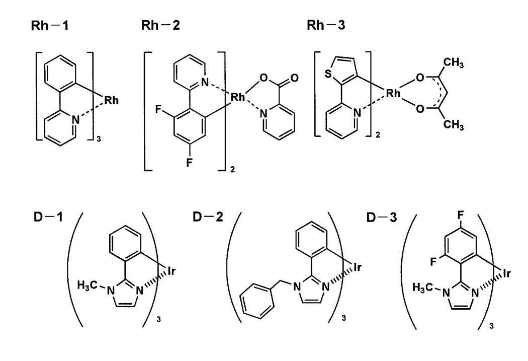
注入層は必要に応じて設け、電子注入層と正孔注入層があり、上記の如く陽極と発光層または正孔輸送層の間、及び陰極と発光層または電子輸送層との間に存在させてもよい。
阻止層は、上記の如く有機化合物薄膜の基本構成層の他に必要に応じて設けられるものである。例えば、特開平11-204258号公報、同11-204359号公報、及び「有機EL素子とその工業化最前線(1998年11月30日エヌ・ティー・エス社発行)」の237頁等に記載されている正孔阻止(ホールブロック)層がある。
正孔輸送層とは、正孔を輸送する機能を有する正孔輸送材料からなり、広い意味で正孔注入層、電子阻止層も正孔輸送層に含まれる。正孔輸送層は単層または複数層設けることができる。
電子輸送層とは、電子を輸送する機能を有する材料からなり、広い意味で電子注入層、正孔阻止層も電子輸送層に含まれる。電子輸送層は単層または複数層設けることができる。
本発明に係る有機EL構造体の作製方法の一例として、陽極/正孔注入層/正孔輸送層/発光層/正孔阻止層/電子輸送層/陰極からなる有機EL構造体の作製法について説明する。
本発明では、可撓性の基材の上に、第1電極、少なくとも1層の有機層及び第2電極を有する有機EL構造体を形成した後、前記有機EL構造体上に可撓性の封止基材を貼合し、前記基材のTg(ガラス転移点)未満で、かつ下記封止基材のTg(ガラス転移点)以上の温度で熱処理することが特徴である。基材と封止基材のTgの差は30~50℃が好ましく、好ましい基材-封止基材の組合せは、延伸PEN-延伸PET、延伸PEN-無延伸PET、無延伸PEN-無延伸PET、延伸PEN-無延伸PETである。熱処理の温度は、基材のTg未満でかつ封止基材のTg以上で、絶対値としては100~140℃が好ましい。
本発明に係る封止基材は、有機EL素子を封止し、当該素子を温度変化、湿度、酸素、衝撃等の過酷な外部環境から守るためのものである。
ポリプロピレン -20℃
ポリ塩化ビニル 80℃
ポリスチレン 100℃
ポリカーボネート 150℃
無延伸PET 80℃
無延伸PEN 120℃
延伸PET 110℃
延伸PEN 155℃
樹脂フィルムとしては上記の他に、ナイロン(Ny)、塩化ビニリデン(PVDC)をコートしたナイロン(KNy)、PVDCをコートしたポリプロピレン(KOP)、PVDCをコートしたセロハン(KPT)、ポリエチレン-ビニルアルコール共重合体(エバール)を用いることが可能である。また、これら樹脂フィルムは、必要に応じて異種フィルムと共押し出しで作った多層フィルム、延伸角度を変えて張り合わせ積層した多層フィルム等も当然使用できる。さらに必要とする包装材料の物性を得るために使用するフィルムの密度、分子量分布を組み合わせて作ることも当然可能である。本発明では、多層フィルムの封止基材のTgは、構成する樹脂の内最もTgが低い樹脂のTgと定義する。
封止基材を接着するための接着剤としては、アクリル酸系オリゴマー、メタクリル酸系オリゴマーの反応性ビニル基を有する熱硬化型接着剤等を挙げることができる。市販品としては、スリーボンド1152、1153等を使用することができる。
本発明に係る有機EL構造体の製造装置及びそれを用いた製造方法(プロセス)の一例について、図3を参照して説明する。
図4は、封止基材層形成工程140及び断裁工程150の1例を示す模式図である。
(第一電極の形成)
厚さ100μm、幅200mm、長さ500mのポリエチレンナフタレートフィルム(帝人・デュポン社製フィルム、以下、PENと略記する)に、バリア膜を形成した基材(特開2007-83644号の実施例1に記載の方法で形成した)を準備した。なお、基材には、予め第一電極を形成する位置を示すためにアライメントマークを設け、5×10⁻¹Paの真空環境条件で厚さ120nmのITO(インジウムチンオキシド)をスパッタリング法により、マスクパターン成膜を行い、引き出し部を基材の巾手方向の両端側に有する10mm×10mmの大きさの第一電極を一定間隔に12列を連続的に形成し巻き取った。
ポリエチレンジオキシチオフェン・ポリスチレンスルホネート(PEDOT/PSS、Bayer社製 Bytron P AI 4083)を純水で65%、メタノール5質量%で希釈した溶液を第一正孔輸送層形成用塗布液として、基材上全面(但し、両端の10mmは除く)に、押し出し塗布機を使用し乾燥後の厚みが30nmになるように塗布した。塗布後、乾燥・加熱処理を行い、第一正孔輸送層を形成した。
第一正孔輸送層形成用塗布液の塗布条件は、温度は25℃、露点温度-20℃以下のN2ガス環境の大気圧下で、且つ清浄度クラス5以下(JIS B 9920)で行った。
第一正孔輸送層が形成された基材に、マイクロ波(2.45GHz)を照射して第一電極を熱パターンとしてその位置を検出して、これを位置決めマークとして用い、第一電極の取り出し電極部分の上及び第一電極の周囲の不要の部分に、正孔輸送層に対してこれを膨潤させる良溶媒であるメチルエチルケトンを供給して、図5の拭き取り装置により、装置内温度10℃で1.96×10⁵Pa程度の押圧でワイピングヘッド(押圧ロール及びテープ状部材)の基材との相対速度が5cm/秒となるよう擦って、有機エレクトロニクス構造体の間を連続的に拭き取り除去した。なお、温度は5℃、メチルエチルケトンの蒸気圧は5℃において4173Paである。また、マイクロ波照射機は四国計測工業(株)製 μ-reactorを用いた。
窒素雰囲気下で、50mgの正孔輸送材料1(下記)を10mlのトルエンに溶解した溶液を押し出し塗布法により製膜した。乾燥後、窒素雰囲気下、180秒間紫外光を照射し、光重合・架橋を行い、膜厚約20nmの第二正孔輸送層を形成した。
第二正孔輸送層上に、PVK、ドーパント4をそれぞれ1質量%、0.1質量%含むトルエン溶液を押し出し塗布法により製膜した。120℃で乾燥し、膜厚約50nmの発光層とした。
発光層上に、0.5質量%の電子輸送材料1を含有する1-ブタノール溶液を同様に押し出し塗布法により製膜した。60℃で乾燥し、膜厚約15nmの電子輸送層とした。
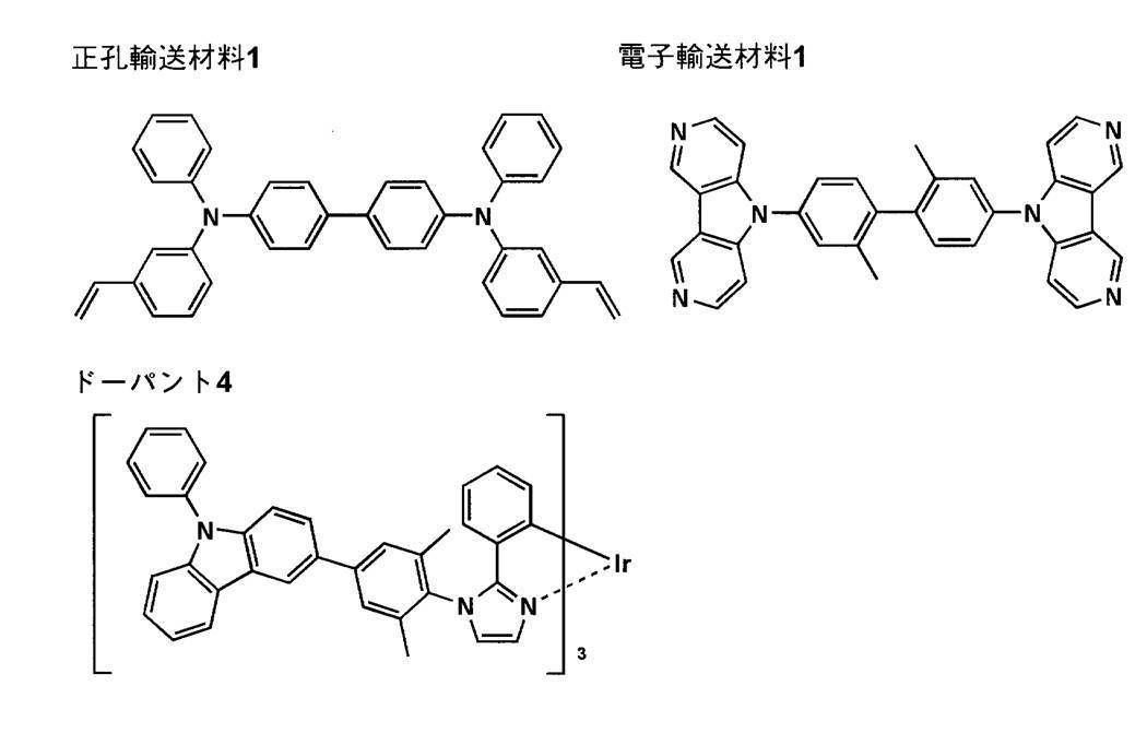
巻き取った前記、第一正孔輸送層が形成された基材を供給して、基材上に形成された第一電極パターンを位置決めマークとして、マイクロ波センサを用いて、位置決めを行い、第一電極の取り出し電極部分の上及び第一電極の周囲の不要の部分を、図7の拭き取り装置により、第二正孔輸送層、発光層に対し親和性が高い溶剤であるo-キシレン、電子輸送層に対して良溶媒である1-ブタノールをそれぞれ2:1の混合比で混合した溶剤を供給して、温度15℃、前記同様、押圧ロール(テープ状部材)の基材との相対速度が5cm/秒となるよう擦って連続的に拭き取り除去した。なお、ワイピングヘッドの押圧は1.96×105Paとした。拭き取り温度は、拭き取り装置内を15℃まで冷却して溶剤のトータルの供給量は20ml/minで行った。
パターン化された有機層が形成されたロール状の基材に付けられた陽極の位置に従って電子輸送層の上及び第一電極の引き出し部を除いた部分に蒸着装置で5×10⁻⁴Paの真空環境条件にてLiFを用い、マスクパターン蒸着成膜して、厚さ0.5nmの陰極バッファー層(電子注入層)を積層した。
引き続き、同様に陰極バッファー層(電子注入層)上に第一電極の大きさに合わせ、第一電極の引き出し部と反対側に第二電極の引き出し部が配置されるように、5×10⁻⁴Paの真空下にてアルミニウムを使用し蒸着法にてマスクパターン成膜し、厚さ100nmのアルミニウム層からなる第二電極を積層し有機EL構造体を形成した。
次いで、有機EL構造体を有する基材に付けられたアライメントマークを検出し、アライメントマークの位置に従って第一電極及び第二電極の引き出し部の一部を除いて、接着剤層を有する長尺の封止基材を貼合した。
封止基材貼合後に、100℃で1時間熱硬化を行った。
次いで、作製した複数の有機EL構造体を有する基材を個別の有機EL素子の大きさに、アライメントマークを検出し、アライメントマークの位置に従って断裁し、有機EL素子1を得た。
有機EL素子1の作製において、基材の樹脂、封止基材の樹脂、及び貼合後の熱処理温度を表1のように変更した以外は同様にして有機EL素子2~15を作製した。
上記の方法により作製した有機EL素子について、発光ムラ及び発光割合を測定し評価した。
KEITHLEY社製ソースメジャーユニット2400型を用いて、直流電圧を有機EL素子に印加し200cd/cm2で発光させた。50倍の顕微鏡で発光ムラを観察し、下記基準で評価した。
○:実技上問題とならない僅かな発光ムラがある
×:均一発光部分が7割未満である実技上問題となる発光ムラがある
(発光面積(バリア性))
温度25℃にて減圧環境33330Paに24時間保存後、加速劣化条件下(60℃90%RH、250時間)で保存後のダークスポット等の未発光部を除く発光部の面積を測定した。初期発光面積との比率を下記基準で評価した。
○:95%未満~90%以上
△:90%未満~85%以上
×:85%未満
評価の結果を表1に示す。
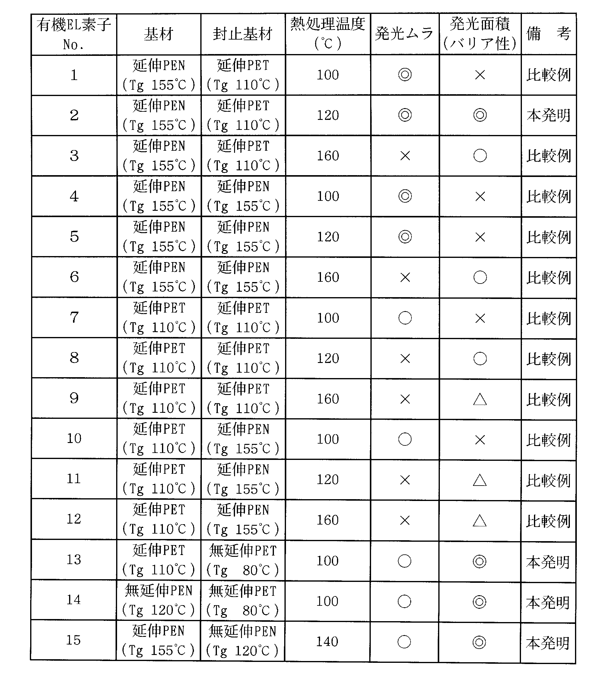
実施例1の有機EL素子2の作製において、正孔注入層を形成した後、下記発電層塗布液を塗布し、120℃で乾燥し、乾燥後の厚さが150nmの原反ウェブを作製した以外は、有機EL素子2の作製と同様にして、乾燥剤を素子内に有する有機光電変換素子を作製した。
クロロベンゼン6mlに、数平均分子量45000のレジオレギュラーP3HT(ポリ-3-ヘキシルチオフェン)と、フラーレン誘導体PCBM(6,6-フェニル-C61-ブチル酸メチルエステル)を質量比が1:1で、3質量%となるように溶解した溶液を用いた。製膜後、140℃の乾燥ゾーンをゆっくり搬送しながら、窒素気流下で乾燥し、乾燥膜厚150nmの発電層を形成した。
2 有機EL構造体
3′ 供給工程
301′ 基材
4′ 正孔輸送層形成工程
5′ 発光層形成工程
5′a 第1塗布工程
5′a1 静電ノズル吐出装置
5′b 第1乾燥工程
5′c 第2塗布工程
5′c1 静電ノズル吐出装置
5′d 第2乾燥工程
5′e 第3塗布工程
5′e1 静電ノズル吐出装置
5′f 第3乾燥工程
7′ 電子注入層形成工程
8′ 第2電極形成工程
9′ 保護層形成工程
10 回収工程
11、12 基材
16 封止基材層
16A 接着剤
16B 封止基材(封止フィルム)
111 拭き取り装置の基台
112 拭き取りユニット
115 テープ状部材
116 送り出しロール
117 巻き取りロール
118 溶剤保持タンク
119 供給パイプ
121 押圧ロール
122 シリンダ
140 封止基材層形成工程
150 断裁工程
151A 断裁刃
Claims (5)
- 可撓性の基材の上に、第1電極、少なくとも1層の有機層及び第2電極を有する有機エレクトロニクス構造体を形成した後、前記有機エレクトロニクス構造体上に可撓性の封止基材を貼合し、熱処理する有機エレクトロニクス素子の製造方法において、前記熱処理の温度が前記基材のTg(ガラス転移点)未満で、かつ前記封止基材のTg(ガラス転移点)以上であることを特徴とする有機エレクトロニクス素子の製造方法。
- 前記封止基材にバリア膜が形成されていることを特徴とする請求項1に記載の有機エレクトロニクス素子の製造方法。
- 前記基材が長尺基材であることを特徴とする請求項1または2に記載の有機エレクトロニクス素子の製造方法。
- 前記有機エレクトロニクス素子が、有機エレクトロルミネッセンス素子であることを特徴とする請求項1~3のいずれか1項に記載の有機エレクトロニクス素子の製造方法。
- 請求項1~4のいずれか1項に記載の有機エレクトロニクス素子の製造方法により製造されたことを特徴とする有機エレクトロニクス素子。
Priority Applications (2)
| Application Number | Priority Date | Filing Date | Title |
|---|---|---|---|
| US13/254,886 US8455283B2 (en) | 2009-03-13 | 2010-03-03 | Organic electronic element and its manufacturing method |
| JP2011503779A JP5494648B2 (ja) | 2009-03-13 | 2010-03-03 | 有機エレクトロニクス素子及びその製造方法 |
Applications Claiming Priority (2)
| Application Number | Priority Date | Filing Date | Title |
|---|---|---|---|
| JP2009-061042 | 2009-03-13 | ||
| JP2009061042 | 2009-03-13 |
Publications (1)
| Publication Number | Publication Date |
|---|---|
| WO2010103967A1 true WO2010103967A1 (ja) | 2010-09-16 |
Family
ID=42728257
Family Applications (1)
| Application Number | Title | Priority Date | Filing Date |
|---|---|---|---|
| PCT/JP2010/053411 Ceased WO2010103967A1 (ja) | 2009-03-13 | 2010-03-03 | 有機エレクトロニクス素子及びその製造方法 |
Country Status (3)
| Country | Link |
|---|---|
| US (1) | US8455283B2 (ja) |
| JP (1) | JP5494648B2 (ja) |
| WO (1) | WO2010103967A1 (ja) |
Cited By (8)
| Publication number | Priority date | Publication date | Assignee | Title |
|---|---|---|---|---|
| WO2011052630A1 (ja) * | 2009-10-28 | 2011-05-05 | コニカミノルタホールディングス株式会社 | 有機エレクトロルミネッセンスパネルの製造方法、有機エレクトロルミネッセンスパネル |
| WO2012046742A1 (ja) * | 2010-10-08 | 2012-04-12 | 住友化学株式会社 | 有機el装置 |
| WO2012046736A1 (ja) * | 2010-10-08 | 2012-04-12 | 住友化学株式会社 | 有機el装置及びその製造方法 |
| WO2012147658A1 (ja) * | 2011-04-25 | 2012-11-01 | 株式会社ニコン | 基板処理装置 |
| JP2014120479A (ja) * | 2012-12-17 | 2014-06-30 | Universal Display Corp | フレキシブル有機電子デバイスの製造 |
| JP2014214366A (ja) * | 2013-04-26 | 2014-11-17 | コニカミノルタ株式会社 | プラズマcvd成膜用マスク、プラズマcvd成膜方法、及び有機エレクトロルミネッセンス素子 |
| JP2014214367A (ja) * | 2013-04-26 | 2014-11-17 | コニカミノルタ株式会社 | プラズマcvd成膜用マスク、プラズマcvd成膜方法、及び有機エレクトロルミネッセンス素子 |
| JP2017162725A (ja) * | 2016-03-10 | 2017-09-14 | 住友化学株式会社 | 有機デバイスの製造方法 |
Families Citing this family (8)
| Publication number | Priority date | Publication date | Assignee | Title |
|---|---|---|---|---|
| JP5478147B2 (ja) * | 2009-08-19 | 2014-04-23 | リンテック株式会社 | 発光シート及びその製造方法 |
| US20130236681A1 (en) * | 2012-03-06 | 2013-09-12 | Chang Min Lee | Photocurable composition, barrier layer including the same, and encapsulated apparatus including the same |
| US20160233425A1 (en) * | 2013-10-01 | 2016-08-11 | Sumitomo Chemical Company, Limited | Light emitting device |
| JP6286024B2 (ja) * | 2014-03-07 | 2018-02-28 | 富士フイルム株式会社 | トランジスタの製造方法 |
| KR101829971B1 (ko) | 2015-02-17 | 2018-02-19 | 주식회사 엘지화학 | 봉지 필름 |
| EP3316351A1 (en) * | 2016-10-27 | 2018-05-02 | Lithium Energy and Power GmbH & Co. KG | A system and a method for testing a battery cell |
| JP6962947B2 (ja) * | 2019-02-22 | 2021-11-05 | 株式会社東芝 | 放射線検出器 |
| KR102752729B1 (ko) * | 2020-10-16 | 2025-01-10 | 주식회사 엘지에너지솔루션 | 전극 정렬부를 포함하는 전극 제조장치 및 이를 포함하는 전극조립체 제조장치 |
Citations (10)
| Publication number | Priority date | Publication date | Assignee | Title |
|---|---|---|---|---|
| JP2001057287A (ja) * | 1999-08-20 | 2001-02-27 | Tdk Corp | 有機el素子 |
| JP2003264073A (ja) * | 2002-03-08 | 2003-09-19 | Fuji Electric Co Ltd | 有機elディスプレイの製造方法 |
| JP2004111380A (ja) * | 2002-08-29 | 2004-04-08 | Toray Ind Inc | 有機電界発光素子封止用樹脂組成物、有機電界発光素子及び有機電界発光素子の封止方法 |
| JP2004134279A (ja) * | 2002-10-11 | 2004-04-30 | Tohoku Pioneer Corp | 有機el表示パネル及びその製造方法 |
| JP2005108653A (ja) * | 2003-09-30 | 2005-04-21 | Sanyo Electric Co Ltd | 有機電界発光装置およびその製造方法 |
| JP2005205683A (ja) * | 2004-01-21 | 2005-08-04 | Hitachi Maxell Ltd | 樹脂基板およびその製造方法 |
| JP2006236791A (ja) * | 2005-02-25 | 2006-09-07 | Tohoku Pioneer Corp | 表示パネルの製造方法 |
| JP2007266161A (ja) * | 2006-03-28 | 2007-10-11 | Canon Inc | 有機発光素子アレイ |
| JP2007284472A (ja) * | 2006-04-12 | 2007-11-01 | Shin Etsu Chem Co Ltd | エンドシール材 |
| JP2007287557A (ja) * | 2006-04-19 | 2007-11-01 | Matsushita Electric Ind Co Ltd | 有機半導体デバイス、これを用いた光ヘッドおよび画像形成装置 |
Family Cites Families (2)
| Publication number | Priority date | Publication date | Assignee | Title |
|---|---|---|---|---|
| JP2003077669A (ja) | 2001-09-03 | 2003-03-14 | Toppan Printing Co Ltd | 高分子エレクトロルミネッセンス素子及びその製造方法 |
| WO2005096675A1 (ja) | 2004-03-31 | 2005-10-13 | Pioneer Corporation | 発光パネルの製造方法 |
-
2010
- 2010-03-03 JP JP2011503779A patent/JP5494648B2/ja not_active Expired - Fee Related
- 2010-03-03 US US13/254,886 patent/US8455283B2/en active Active
- 2010-03-03 WO PCT/JP2010/053411 patent/WO2010103967A1/ja not_active Ceased
Patent Citations (10)
| Publication number | Priority date | Publication date | Assignee | Title |
|---|---|---|---|---|
| JP2001057287A (ja) * | 1999-08-20 | 2001-02-27 | Tdk Corp | 有機el素子 |
| JP2003264073A (ja) * | 2002-03-08 | 2003-09-19 | Fuji Electric Co Ltd | 有機elディスプレイの製造方法 |
| JP2004111380A (ja) * | 2002-08-29 | 2004-04-08 | Toray Ind Inc | 有機電界発光素子封止用樹脂組成物、有機電界発光素子及び有機電界発光素子の封止方法 |
| JP2004134279A (ja) * | 2002-10-11 | 2004-04-30 | Tohoku Pioneer Corp | 有機el表示パネル及びその製造方法 |
| JP2005108653A (ja) * | 2003-09-30 | 2005-04-21 | Sanyo Electric Co Ltd | 有機電界発光装置およびその製造方法 |
| JP2005205683A (ja) * | 2004-01-21 | 2005-08-04 | Hitachi Maxell Ltd | 樹脂基板およびその製造方法 |
| JP2006236791A (ja) * | 2005-02-25 | 2006-09-07 | Tohoku Pioneer Corp | 表示パネルの製造方法 |
| JP2007266161A (ja) * | 2006-03-28 | 2007-10-11 | Canon Inc | 有機発光素子アレイ |
| JP2007284472A (ja) * | 2006-04-12 | 2007-11-01 | Shin Etsu Chem Co Ltd | エンドシール材 |
| JP2007287557A (ja) * | 2006-04-19 | 2007-11-01 | Matsushita Electric Ind Co Ltd | 有機半導体デバイス、これを用いた光ヘッドおよび画像形成装置 |
Cited By (15)
| Publication number | Priority date | Publication date | Assignee | Title |
|---|---|---|---|---|
| WO2011052630A1 (ja) * | 2009-10-28 | 2011-05-05 | コニカミノルタホールディングス株式会社 | 有機エレクトロルミネッセンスパネルの製造方法、有機エレクトロルミネッセンスパネル |
| JPWO2011052630A1 (ja) * | 2009-10-28 | 2013-03-21 | コニカミノルタホールディングス株式会社 | 有機エレクトロルミネッセンスパネルの製造方法、有機エレクトロルミネッセンスパネル |
| JP2012084306A (ja) * | 2010-10-08 | 2012-04-26 | Sumitomo Chemical Co Ltd | 有機el装置 |
| WO2012046736A1 (ja) * | 2010-10-08 | 2012-04-12 | 住友化学株式会社 | 有機el装置及びその製造方法 |
| JP2012084308A (ja) * | 2010-10-08 | 2012-04-26 | Sumitomo Chemical Co Ltd | 有機el装置 |
| WO2012046742A1 (ja) * | 2010-10-08 | 2012-04-12 | 住友化学株式会社 | 有機el装置 |
| WO2012147658A1 (ja) * | 2011-04-25 | 2012-11-01 | 株式会社ニコン | 基板処理装置 |
| JPWO2012147658A1 (ja) * | 2011-04-25 | 2014-07-28 | 株式会社ニコン | 基板処理装置およびデバイス製造方法 |
| TWI595579B (zh) * | 2011-04-25 | 2017-08-11 | 尼康股份有限公司 | 基板處理裝置 |
| JP2014120479A (ja) * | 2012-12-17 | 2014-06-30 | Universal Display Corp | フレキシブル有機電子デバイスの製造 |
| JP2018107134A (ja) * | 2012-12-17 | 2018-07-05 | ユニバーサル ディスプレイ コーポレイション | フレキシブル有機電子デバイスの製造 |
| JP2014214366A (ja) * | 2013-04-26 | 2014-11-17 | コニカミノルタ株式会社 | プラズマcvd成膜用マスク、プラズマcvd成膜方法、及び有機エレクトロルミネッセンス素子 |
| JP2014214367A (ja) * | 2013-04-26 | 2014-11-17 | コニカミノルタ株式会社 | プラズマcvd成膜用マスク、プラズマcvd成膜方法、及び有機エレクトロルミネッセンス素子 |
| JP2017162725A (ja) * | 2016-03-10 | 2017-09-14 | 住友化学株式会社 | 有機デバイスの製造方法 |
| WO2017154575A1 (ja) * | 2016-03-10 | 2017-09-14 | 住友化学株式会社 | 有機デバイスの製造方法 |
Also Published As
| Publication number | Publication date |
|---|---|
| JP5494648B2 (ja) | 2014-05-21 |
| US8455283B2 (en) | 2013-06-04 |
| US20110315972A1 (en) | 2011-12-29 |
| JPWO2010103967A1 (ja) | 2012-09-13 |
Similar Documents
| Publication | Publication Date | Title |
|---|---|---|
| JP5494648B2 (ja) | 有機エレクトロニクス素子及びその製造方法 | |
| JP5157440B2 (ja) | 有機el素子の製造方法 | |
| JP5418505B2 (ja) | 有機エレクトロニクス素子及びその製造方法 | |
| JP5093049B2 (ja) | 有機エレクトロニクス素子、その製造方法、及び製造装置 | |
| JP5055711B2 (ja) | 有機el素子の製造方法、有機el素子 | |
| JP5125503B2 (ja) | 有機el素子の製造方法 | |
| JP6111822B2 (ja) | 有機エレクトロルミネッセンス素子の製造方法及び製造装置 | |
| JPWO2007034647A1 (ja) | 有機エレクトロルミネッセンス素子の製造方法、有機エレクトロルミネッセンス表示装置 | |
| JP5652405B2 (ja) | 有機el素子の製造方法 | |
| JPWO2007004627A1 (ja) | パターニング装置、有機エレクトロルミネッセンス素子とその製造方法及び有機エレクトロルミネッセンス表示装置 | |
| JP5104301B2 (ja) | 有機エレクトロルミネッセンスパネルの製造方法 | |
| JP5018317B2 (ja) | 有機エレクトロルミネッセンス素子の製造方法 | |
| JPWO2008102867A1 (ja) | 有機エレクトロルミネッセンス素子、有機エレクトロルミネッセンス素子の製造方法 | |
| JP2012128954A (ja) | 有機エレクトロルミネッセンス素子の製造方法および有機エレクトロルミネッセンス素子 | |
| JP5575353B2 (ja) | 有機エレクトロルミネッセンス素子の製造方法 | |
| JP5092756B2 (ja) | 有機エレクトロルミネッセンスパネルの製造方法、有機エレクトロルミネッセンス照明装置および有機エレクトロルミネッセンスパネルの製造装置 | |
| JP4957643B2 (ja) | 有機化合物層形成用塗布液の塗布方法 | |
| JP5472107B2 (ja) | 有機エレクトロルミネセンス素子の製造方法 | |
| JP2007207469A (ja) | 積層体の製造方法、積層体、有機エレクトロルミネッセンス素子の製造方法、有機エレクトロルミネッセンス素子、有機エレクトロルミネッセンス表示装置 | |
| JP5862439B2 (ja) | 有機半導体素子及びその製造方法 | |
| JP5170102B2 (ja) | 有機エレクトロニクス素子の製造方法 | |
| JP2011049084A (ja) | 有機エレクトロルミネッセンスパネルの製造方法 | |
| JP2008117689A (ja) | 機能性積層膜の形成方法、積層薄膜デバイス、有機エレクトロルミネッセンス表示装置 | |
| JP2013143346A (ja) | 有機el素子の製造方法 | |
| JP2007115573A (ja) | 有機エレクトロルミネッセンス素子の製造方法、有機エレクトロルミネッセンス表示装置 |
Legal Events
| Date | Code | Title | Description |
|---|---|---|---|
| 121 | Ep: the epo has been informed by wipo that ep was designated in this application |
Ref document number: 10750721 Country of ref document: EP Kind code of ref document: A1 |
|
| WWE | Wipo information: entry into national phase |
Ref document number: 2011503779 Country of ref document: JP |
|
| WWE | Wipo information: entry into national phase |
Ref document number: 13254886 Country of ref document: US |
|
| NENP | Non-entry into the national phase |
Ref country code: DE |
|
| 122 | Ep: pct application non-entry in european phase |
Ref document number: 10750721 Country of ref document: EP Kind code of ref document: A1 |