WO2010101023A1 - 平行移動機構および平行移動機構の製造方法 - Google Patents
平行移動機構および平行移動機構の製造方法 Download PDFInfo
- Publication number
- WO2010101023A1 WO2010101023A1 PCT/JP2010/052423 JP2010052423W WO2010101023A1 WO 2010101023 A1 WO2010101023 A1 WO 2010101023A1 JP 2010052423 W JP2010052423 W JP 2010052423W WO 2010101023 A1 WO2010101023 A1 WO 2010101023A1
- Authority
- WO
- WIPO (PCT)
- Prior art keywords
- layer
- moving
- oxide film
- intermediate layer
- support
- Prior art date
- Legal status (The legal status is an assumption and is not a legal conclusion. Google has not performed a legal analysis and makes no representation as to the accuracy of the status listed.)
- Ceased
Links
Images







Classifications
-
- B—PERFORMING OPERATIONS; TRANSPORTING
- B81—MICROSTRUCTURAL TECHNOLOGY
- B81B—MICROSTRUCTURAL DEVICES OR SYSTEMS, e.g. MICROMECHANICAL DEVICES
- B81B3/00—Devices comprising flexible or deformable elements, e.g. comprising elastic tongues or membranes
- B81B3/0035—Constitution or structural means for controlling the movement of the flexible or deformable elements
- B81B3/0051—For defining the movement, i.e. structures that guide or limit the movement of an element
-
- G—PHYSICS
- G02—OPTICS
- G02B—OPTICAL ELEMENTS, SYSTEMS OR APPARATUS
- G02B7/00—Mountings, adjusting means, or light-tight connections, for optical elements
- G02B7/02—Mountings, adjusting means, or light-tight connections, for optical elements for lenses
- G02B7/04—Mountings, adjusting means, or light-tight connections, for optical elements for lenses with mechanism for focusing or varying magnification
- G02B7/08—Mountings, adjusting means, or light-tight connections, for optical elements for lenses with mechanism for focusing or varying magnification adapted to co-operate with a remote control mechanism
-
- B—PERFORMING OPERATIONS; TRANSPORTING
- B81—MICROSTRUCTURAL TECHNOLOGY
- B81B—MICROSTRUCTURAL DEVICES OR SYSTEMS, e.g. MICROMECHANICAL DEVICES
- B81B2201/00—Specific applications of microelectromechanical systems
- B81B2201/02—Sensors
- B81B2201/0228—Inertial sensors
- B81B2201/0235—Accelerometers
Definitions
- the present invention relates to a translation mechanism and a method for manufacturing the translation mechanism, and more particularly to a translation mechanism formed by MEMS technology and a method for manufacturing the translation mechanism.
- a parallel movement mechanism using a parallel link mechanism has been used as a vehicle suspension or stage movement mechanism.
- two members having rotation fulcrums at both ends are arranged in parallel, so that a member held between the fulcrums can be translated.
- MEMS Micro Electro Mechanical Systems
- the shape can be transferred and etched using a photolithographic technique on a large-area silicon wafer, and fine shapes can be collectively formed with high accuracy, thereby realizing downsizing and cost reduction.
- Patent Document 1 discloses a mechanism in which a two-layer link mechanism extending in the surface direction is provided and moved in the surface direction.
- Patent Document 2 discloses a mechanism that is provided with a two-layer link mechanism extending in the thickness direction and moves in the surface direction.
- Patent Document 3 discloses a mechanism in which a single link mechanism extending in the surface direction is provided and moved in a direction perpendicular to the surface.
- JP 2000-314842 A JP 2005-262357 A JP 2000-339725 A
- the present invention has been made in view of the above circumstances, and is capable of suppressing tilting and positional deviation of optical components, enabling a small amount of highly accurate parallel movement, and obtaining a large displacement with a small driving force. It is an object of the present invention to provide a mechanism and a method for manufacturing a translation mechanism.
- the object of the present invention can be achieved by the following configuration.
- a moving part formed by laminating a first layer on at least part of the upper surface of the intermediate layer and laminating a second layer on at least part of the lower surface of the intermediate layer;
- the first layer is stacked on at least part of the upper surface of the intermediate layer
- the second layer is stacked on at least part of the lower surface of the intermediate layer, facing at least the moving part.
- a support provided at a position; A first beam formed of the first layer connecting the first layer of the moving part and the first layer of the support part facing the first layer of the moving part; , A second beam formed of the second layer connecting the second layer of the moving unit and the second layer of the support unit facing the second layer of the moving unit;
- a translation mechanism characterized in that the translation part is capable of translation in the stacking direction of the first layer, the intermediate layer, and the second layer.
- the support part is provided at a position sandwiching at least the moving part
- the first beam is provided with at least two, and connects the first layer of the moving unit and the first layer of the support unit facing the first layer of the moving unit
- At least two of the second beams are provided, and connect the second layer of the moving unit and the second layer of the support unit facing the second layer of the moving unit.
- the moving part has an opening penetrating in the stacking direction of each layer forming the moving part, 5.
- the parallel movement mechanism according to any one of 1 to 4, wherein a lens is inserted into the opening with an optical axis directed in the stacking direction.
- a driving layer for translating the moving unit in a stacking direction of the first layer, the intermediate layer, and the second layer is provided on one plane of the moving unit. 7.
- the parallel movement mechanism according to any one of 1 to 6.
- a resist agent is applied on the first layer, and is configured by a photolithography method, which includes a portion that becomes a moving portion, a portion that becomes a supporting portion, and the first layer, and the moving portion and the supporting portion, A first photolithography step of forming a mask pattern in a portion to be a first beam connecting the two; A first etching step of removing portions of the first layer, the first oxide film, and the intermediate layer other than the moving portion, the support portion, and the first beam by etching; A first resist agent removing step of removing the resist agent remaining on the first layer;
- the moving portion formed by laminating the first layer on the upper surface of the intermediate layer and the second layer on the lower surface is formed on the supporting portion similarly formed by the first layer. Connected by the formed first beam and the second beam formed by the second layer so that the moving part can move in parallel in the stacking direction of the first layer, the intermediate layer and the second layer.
- FIG. 1 shows a configuration of the first embodiment of the translation mechanism according to the present invention.
- 1A is a plan view
- FIG. 1B is a cross-sectional view along AA ′ in FIG. 1A
- FIG. 1C is a cross-sectional view along BB ′ in FIG. 1A.
- 2A and 2B are schematic views showing the operation of the first embodiment of the translation mechanism according to the present invention.
- FIG. 2A shows a state before the operation
- FIG. 2B shows a state after the operation.
- the parallel movement mechanism 1 includes a moving part 11, a support part 13, two first beams 15 and four second beams 17 and the like.
- the support unit 13 is arranged so as to surround the moving unit 11, and the moving unit 11 and the support unit 13 are provided on each of two opposite sides of the moving unit 11 in the y direction as illustrated. 1B, and as shown in FIG. 1B, four second beams provided on both sides in the x direction of the first beam 15 on the back surface side of the figure. 17 are connected.
- the moving unit 11 and the support unit 13 are configured by laminating three parallel plate-shaped layers of a first layer 101, an intermediate layer 301, and a second layer 201.
- the first layer 101, the intermediate layer 301, and the second layer 201 are, for example, silicon (Si), and the interface of the intermediate layer 301 with the first layer 101 and the second layer 201 is the first oxide film.
- a (SiO 2 ) 303 and a second oxide film (SiO 2 ) 305 are formed.
- the first layer 101 and the second layer 201 are equal in thickness.
- the first beam 15 is composed only of the first layer 101
- the second beam 17 is composed only of the second layer 201. Therefore, the moving unit 11 and the support unit 13 are connected to each other by the first beam 15 configured by the first layer 101 on the upper surface side and the second beam 17 configured by the second layer 201 on the lower surface side. Will be linked.
- the first beam 15 and the second beam 17 are equal in length and thickness, and the width of the first beam 15 is twice that of the second beam 17.
- the two second beams 17 are configured to have the same bending rigidity.
- the first beam 15 and the second beam 17 have an axisymmetric shape in the x direction and the y direction, and the entire parallel movement mechanism 1 has the same rigidity against deformation in the z direction.
- the support portion 13 is arranged so as to surround the moving portion 11, but this is not essential, and at least the moving portion 11 is composed of the first beam 15 and the second beam 17. If there is a part connected with.
- FIG. 2 is a cross-sectional view taken along the line B-B ′ of FIG. 1C, and the first beam 15 is indicated by a broken line for convenience.
- a driving force F in the z direction is applied from the outside to the moving unit 11 in the state of FIG. 2A, the first beam 15 and the second beam 17 are shown in FIG. 2B. Is deformed into an S shape.
- the parallel movement mechanism 1 As described above, since the parallel movement mechanism 1 as a whole has the same rigidity against deformation in the z direction, it is pushed by the driving force F in the z direction, and the moving unit 11 is translated in the z direction. Even if an unintended force such as gravity or inertia force is applied from the outside, the parallelism of the moving unit 11 is maintained.
- the driving force F an electromagnetic force, which will be described later with reference to FIG. 6 or later, a force due to electromechanical conversion by a piezoelectric element, a shape memory alloy, or the like can be used.
- FIG. 3 is a process diagram illustrating the manufacturing method of the first embodiment
- FIGS. 4 and 5 are cross-sectional views taken along the line A-A ′ of FIG.
- FIG. 1 A first figure 3 will be described below with reference to FIGS. 4 and 5.
- FIG. 1 A first figure 3 will be described below with reference to FIGS. 4 and 5.
- Step S01 oxide film forming process
- the first oxide film (SiO 2 ) 303 is formed on one surface of the intermediate layer 301 by high-temperature treatment of the intermediate layer 301 made of parallel flat plates of thick silicon (Si).
- a second oxide film (SiO 2 ) 305 is formed on the other surface.
- the thickness of the intermediate layer 301 is generally about 300 to 500 ⁇ m although it depends on specifications such as flatness and mass required for the translation mechanism 1.
- the thicknesses of the first oxide film 303 and the second oxide film 305 are determined by an etching process described later, but are generally 1 ⁇ m or less.
- Step S03 jointing process
- a silicon (Si) thin plate 101 is bonded onto the first oxide film 303
- a silicon (Si) thin plate 201 is bonded onto the second oxide film 305.
- Bonding can be performed by room-temperature bonding in which the surfaces are cleaned and activated by plasma or the like, and anodic bonding using an electric field.
- Step S05 polishing process
- the thin plate 101 and the thin plate 201 joined in step S03 are polished thinly.
- the thicknesses of the polished thin plate 101 and thin plate 201 are determined by the rigidity required for the first beam 15 and the second beam 17, but are generally about several ⁇ m.
- the first layer 101 and the second layer 201 are formed from the thin plate 101 and the thin plate 201.
- the above method is the same as the process of creating a substrate called an SOI (Silicon On Insulator) substrate, and is generally used. Since a plurality of other processes for creating an SOI substrate have been proposed, they may be used.
- SOI Silicon On Insulator
- Step S11 first photolithography process
- a resist agent is applied on the first layer 101, and a mask pattern is formed on a portion to be left in the next first etching process by performing a photolithography process such as exposure and development. 401 is formed.
- Step S13 first etching process
- the first layer 101, the first oxide film 303, the intermediate layer 301, and the second oxide film 305 other than the portion where the mask pattern 401 is formed are removed by etching. Only the second layer 201 is left. Since the reaction material and the rate of etching differ greatly between silicon and oxide, the etching depth can be controlled by controlling the time. Alternatively, the first layer 101, the first oxide film 303, and the intermediate layer 301 may be removed, and the second oxide film 305 and the second layer 201 may be left.
- Step S15 first resist agent removing step
- the resist agent (mask pattern) 401 remaining on the first layer 101 is removed.
- Step S21 (second photolithography process) As shown in FIG. 5B, a resist agent is applied on the second layer 201 and subjected to a photolithography process such as exposure and development, so that a mask pattern is formed on a portion to be left in the next second etching process. 403 is formed.
- a photolithography process such as exposure and development
- Step S23 second etching process
- the second layer 201, the second oxide film 305, the intermediate layer 301, and the first oxide film 303 other than the portion where the mask pattern 403 is formed are removed by etching. , Leaving only the first layer 101.
- the second layer 201, the second oxide film 305, and the intermediate layer 301 may be removed to leave the first oxide film 303 and the first layer 101.
- the etching depth is controlled by controlling the etching time.
- Step S25 second resist agent removing step
- the resist agent (mask pattern) 403 remaining on the second layer 201 is removed.
- the first beam 15 formed only by the first layer 101 and the second beam 17 formed only by the second layer 201 remain, and are the same parallel as shown in FIG. A moving mechanism 1 is formed.
- the moving portion formed by laminating the first layer on the upper surface of the intermediate layer and laminating the second layer on the lower surface is similarly formed.
- the moving portion is connected to the support portion by the first beam formed by the first layer and the second beam formed by the second layer, and the moving portion has the first layer, the intermediate layer, and the second layer.
- FIG. 6 is a schematic diagram showing a first application example of the first embodiment.
- FIG. 6A is a plan view seen from the back side of FIG. 1A
- FIG. 6B is FIG. It is CC 'sectional drawing of (a).
- a hole penetrating from the first layer 101 to the second layer 201 is provided in the center of the moving unit 11 in FIG. 1 (a).
- the lens 21 is inserted with the optical axis 21a directed in the z direction.
- the loop-shaped wiring 31 is provided on the second layer 201 of the moving unit 11, and the permanent magnet 33 is provided at a position facing the wiring 31.
- the support portion 13 and the permanent magnet 33 are fixed to a fixing portion 35 that is a part of the camera body, for example, by adhesion.
- the driving force F can be generated by the action of the current I flowing through the wiring 31 and the magnetic field generated by the permanent magnet 33.
- the driving force F that moves the lens 21 in the negative z direction can be generated by the current I flowing counterclockwise in FIG. If the direction of the current I is reversed, it is possible to generate a driving force F that moves the lens 21 in the positive z direction. Since the moving unit 11 translates in the z direction by the translation mechanism 1, the lens 21 also translates in the z direction, that is, the optical axis 21a direction.
- the parallel movement mechanism according to the first embodiment can be applied to the focus adjustment and zoom mechanism of the camera lens.
- FIG. 7 is a schematic diagram showing a second application example of the first embodiment.
- FIG. 7A is a plan view seen from the same side as FIG. 1A
- FIG. 7C is a sectional view taken along the line DD ′ of FIG.
- a driving element 51 made of a piezoelectric element 501 such as PZT (lead zirconate titanate) sandwiched between two layers of electrodes 503 is disposed on the first layer 101 of the two first beams 15.
- the film is formed by sputtering. This is a so-called unimorph structure. Details of the manufacturing method will be described later with reference to FIG.
- the piezoelectric element 501 when an electric field is applied between the two layers of electrodes 503 of the drive element 51, as shown in FIG. 7C, the piezoelectric element 501 has, for example, an electric field direction, that is, a diagram. Expands in the z direction and contracts in the y direction in the figure. Since the driving element 51 and the first layer 101 of the first beam 15 are in close contact with each other, the piezoelectric element 501 contracts in the y direction, so that the first beam 15 bends in the z direction as in the case of bimetal. The moving unit 11 translates in the positive direction of the z direction with respect to the support unit 13.
- FIG. 8 is a process diagram showing a manufacturing method of a second application example of the first embodiment
- FIG. 9 is a process diagram showing a subroutine of FIG. 8
- FIG. 10 is a process diagram of FIG. FIG. 8 is a sectional view taken along the line DD ′ of FIG. 7 showing a process.
- step S05 polishing process
- step S11 first photolithography process
- step S07 driving element forming subroutine
- step S09 mirror forming subroutine
- step S31 driving element layer forming step
- an electrode 503, a piezoelectric element 501, and another layer of electrode 503 are formed on the first layer 101.
- the drive element layer 51 is formed by film formation in this order by a method such as sputtering.
- step S33 third photolithography process
- a resist agent is applied on the drive element layer 51, and a photolithography process such as exposure and development is performed.
- a mask pattern 407 is left in a portion where the film is to be formed.
- step S35 third etching step
- the electrode 503, the piezoelectric element 501, and the other layer of the electrode 503 other than the portion where the mask pattern 407 is formed are removed by etching. .
- step S37 third resist agent removing step
- the resist agent (mask pattern) 407 remaining on the drive element 51 is removed.
- step S39 the direction of polarization P of the piezoelectric element 501 of the drive element 51 is aligned as shown in FIG. 10E by applying a high voltage between the two layers of electrodes 503. Apply polarization treatment. As a result, the piezoelectric element 501 functions as a drive element.
- the polarization process may be performed after step S25 (second resist agent removing step) in FIG.
- step S39 polarization step
- step S39 polarization step
- step S09 mirror formation subroutine
- the mirror 23 is formed by a method such as vapor deposition. Details are shown in FIG.
- step S41 (fourth photolithography process) a resist agent is applied on the first layer 101 and the driving element 51, and a photolithography process such as exposure and development is performed, whereby a mirror is obtained.
- a mask pattern having an opening is formed in a portion where the portion 23 is to be formed.
- step S43 mirror vapor deposition step
- silver (Ag) or aluminum (Al) is vapor-deposited on the mask pattern formed in step S41.
- step S45 fourth resist agent removing step
- the remaining resist agent that is, the mask pattern is removed, and the mirror 23 is completed.
- step S11 the mask pattern 401 formed on the portion of the first layer 101 that becomes the moving portion 11 in step S11 (first photolithography process) is formed on the mirror 23 described above.
- step S11 first photolithography process
- the driving element 51 that is a member that generates a driving force and the mirror 23 that is an optical functional member can be formed on the parallel movement mechanism 1.
- FIG. 11A and 11B are schematic views showing a third application example of the first embodiment.
- FIG. 11A is a plan view seen from the same side as FIG. 1A
- FIG. 11A is a cross-sectional view taken along line AA ′
- FIG. 11C is a cross-sectional view taken along line BB ′ of FIG.
- the first beam 15 is also indicated by a broken line for convenience.
- the parallel movement mechanism 1 includes a moving part 11, a support part 13, two first beams 15 and four second beams 17 as in FIG. 1A. Has been.
- the support unit 13 is disposed so as to surround the moving unit 11. Similar to the second application example, a mirror 23 is formed on the moving unit 11 by vapor deposition or the like.
- the two first beams 15 are provided so as to straddle a part of the upper surface of two portions of the moving unit 11 facing each other in the y direction and a part of the upper surface of the supporting unit 13 facing the first beam 15. And the support part 13 are connected.
- the four second beams 17 are also provided on the back surface side of the drawing on both sides in the x direction of the first beam 15 and a part of the upper surface of the moving portion 11 and a support opposite thereto.
- the moving part 11 and the support part 13 are connected to each other so as to straddle a part of the upper surface of the part 13.
- loop-shaped wirings 53 of shape memory alloy are formed by a method such as sputtering.
- the moving part 11 and the support part 13 are formed on a first oxide film (SiO 2 ) 303 and a second oxide film on both surfaces of an intermediate layer 301 made of, for example, silicon (Si). (SiO 2 ) 305 is formed.
- the first beam 15 is composed of only the first layer 101, and is provided so as to straddle a part of the upper surface of the moving part 11 and a part of the upper surface of the support part 13 opposed thereto.
- a loop-shaped wiring 53 of a shape memory alloy is formed on the first beam 15.
- the second beam 17 is composed of only the second layer 201, and is provided so as to straddle a part of the lower surface of the moving part 11 and a part of the lower surface of the support part 13 opposed thereto.
- the first layer 101 connects the moving unit 11 and the supporting unit 13 as the first beam 15, and the second layer 201 serves as the second beam 17 and the moving unit 11 and the supporting unit 13. Are linked.
- a loop-shaped wiring 53 of a shape memory alloy as a driving element is formed on the first beam 15, a loop-shaped wiring 53 of a shape memory alloy as a driving element is formed.
- the first beam 15 and the second beam 17 are equal in length and thickness, and the width of the first beam 15 is twice that of the second beam 17.
- the two second beams 17 are configured to have the same bending rigidity.
- the first beam 15 and the second beam 17 have an axisymmetric shape in the x direction and the y direction, and the entire parallel movement mechanism 1 has the same rigidity against deformation in the z direction.
- the shape memory alloy loop-shaped wiring 53 is preliminarily stored with a characteristic that shrinks in the y direction at a high temperature.
- the shape memory alloy loop-shaped wiring 53 When the shape memory alloy loop-shaped wiring 53 is energized, it generates heat due to Joule heat and the high temperature. And contract in the y direction. Accordingly, as in the second application example, the first beam 15 bends in the z direction, and the moving unit 11 translates in the positive direction in the z direction with respect to the support unit 13.
- the manufacturing method of the third application example is almost the same as the manufacturing method of the second application example shown in FIGS.
- the shape memory process for storing the shape in the loop-shaped wiring 53 of the shape memory alloy is not a process corresponding to step S39 (polarization process) in FIG. 9A, but is a step S25 (second resist agent) in FIG. It is necessary to provide after the removal step).
- the driving element 51 that is a member that generates a driving force and the mirror 23 that is an optical functional member are connected to the parallel movement mechanism 1.
- the parallel movement mechanism 1 can be reduced in size and cost.
- FIG. 12A and 12B are schematic views showing the configuration of the second embodiment, in which FIG. 12A is a plan view, FIG. 12B is a cross-sectional view taken along line AA ′ in FIG. ) Is a cross-sectional view along the line DD ′ in FIG.
- the parallel movement mechanism 1 includes a moving part 11, a supporting part 13, two first beams 15, a second beam 17, and the like.
- the support unit 13 is arranged so as to surround the moving unit 11, and the moving unit 11 and the support unit 13 are provided on each of two opposite sides of the moving unit 11 in the y direction as illustrated.
- the first beams 15 are connected to each other, and as shown in FIG. 12C, they are connected to the second beams 17 provided on the entire rear surface side of the drawing.
- the moving part 11 and the support part 13 are configured by laminating three parallel flat plate layers of a first layer 101, an intermediate layer 301, and a resin film layer 203.
- the first layer 101 and the intermediate layer 301 are, for example, silicon (Si), and the interface between the intermediate layer 301 and the first layer 101 is a first oxide film (SiO 2 ) 303.
- the first beam 15 is composed only of the first layer 101
- the second beam 17 is composed only of the resin film layer 203. Therefore, the moving part 11 and the support part 13 are connected by the first beam 15 constituted by the first layer 101 on the upper surface side and the second beam 17 constituted by the resin film layer 203 on the lower surface side. It will be connected.
- the resin film layer 203 Since the resin film layer 203 has high elasticity, it can function as a beam without being subjected to shape processing. Not only the second beam 17 but also the first beam 15 can be configured as a resin film layer.
- the interface between the intermediate layer 301 and the resin film layer 203 may be the second oxide film (SiO 2 ) 305 as in the first embodiment.
- FIG. 13 is a process diagram showing the manufacturing method of the second embodiment
- FIG. 14 is a sectional view taken along the line D-D ′ of FIG. 12A showing each process of FIG. 13.
- step S01 oxide film forming process
- step S15 first resist agent removing process
- the first oxide film (SiO 2 ) 303 and the second oxide film (SiO 2 ) 305, the first layer 101, and the second layer are formed on both surfaces of the intermediate layer 301.
- 201 was formed, and the parallel movement mechanism 1 was formed by performing etching from the first layer 101 side and the second layer 201 side.
- step S41 resin film layer laminating step in FIG. 13, as shown in FIG. 14 (g), on the surface opposite to the first layer 101 of the intermediate layer 301 by a method such as adhesion, The resin film layer 203 is solidly pasted to form the second beam 17, and the translation mechanism 1 is completed.
- the function as the second beam 17 can be achieved without performing shape processing.
- the process for forming the second beam 17 can be simplified, and the manufacturing cost can be reduced. If the first beam 15 is also made of a resin film, the process can be further simplified and the manufacturing cost can be reduced.
- a pair of moving portions 11 and a support portion 13 are a pair of first beams. 15 and the second beam 17.
- the moving unit 11 and the support unit 13 are configured by laminating three parallel flat plate layers of a first layer 101, an intermediate layer 301, and a second layer 201.
- the first layer 101, the intermediate layer 301, and the second layer 201 are, for example, silicon (Si), and the interface between the intermediate layer 301 and the first layer 101 is the same as that of the first oxide film (SiO 2 ) 303. It has become.
- the first beam 15 is composed only of the first layer 101
- the second beam 17 is composed only of the second layer 201.
- the structure of the mechanism is simple, suitable for downsizing, and can be manufactured at low cost.
- the displacement in the y direction occurs when the moving unit 11 moves in the z direction, for example, the driving of the lens 21 as in the first application example of the first embodiment shown in FIG. It cannot be used for those that do not allow displacement in the direction.
- FIG. 16 is a schematic diagram showing a plan for improving the shape of the beam.
- FIG. 16A shows the shape of the beam shown in each of the above-described embodiments and application examples
- FIG. 16B shows the improved beam. An example of a shape is shown.
- the first beam 15 or the second beam 17 that couples the moving unit 11 and the support unit 13 is not a beam having a uniform width as shown in FIG. As shown in FIG. 4, the cutout portions 19 are provided at both ends of the beam.
- the rigidity at both ends of the beam can be lowered and easily deformed, the both ends can be easily deformed, and the center can be easily deformed.
- a parallel movement mechanism close to a typical link mechanism can be realized.
- the moving portion formed by laminating the first layer on the upper surface of the intermediate layer and laminating the second layer on the lower surface is used as the support portion similarly formed.
- the moving part is connected to the first beam, the intermediate layer, and the second layer by connecting the first beam formed of the first layer and the second beam formed of the second layer.
Landscapes
- Physics & Mathematics (AREA)
- General Physics & Mathematics (AREA)
- Optics & Photonics (AREA)
- Engineering & Computer Science (AREA)
- Computer Hardware Design (AREA)
- Microelectronics & Electronic Packaging (AREA)
- Micromachines (AREA)
- Lens Barrels (AREA)
- Mechanical Light Control Or Optical Switches (AREA)
Abstract
中間層の上面に第1の層が積層され、下面に第2の層が積層されて形成された移動部を、同様に形成された支持部に、第1の層で形成された第1の梁と、第2の層で形成された第2の梁とで連結して、移動部が第1の層、中間層および第2の層の積層方向に平行移動可能に構成することで、光学部品の傾きや位置ズレを抑制でき、微小量の高精度な平行移動が可能で、小さな駆動力で大きな変位を得ることができる平行移動機構および平行移動機構の製造方法を提供することができる。
Description
本発明は、平行移動機構および平行移動機構の製造方法に関し、特にMEMS技術により形成される平行移動機構および平行移動機構の製造方法に関する。
従来から、車両のサスペンションやステージの移動機構等に、平行リンク機構を用いた平行移動機構が用いられている。これは、両端に回転支点を備えた二本の梁を平行に配置することにより、支点間に保持された部材を平行移動可能とするものである。
一方、半導体プロセス技術を用いて微細加工を行い、精密部品を作成するMEMS(Micro Electro Mechanical Systems)技術が広がりつつある。これにより、大面積のシリコンウェハに、フォトリソグラフィ技術を用いて形状を転写、蝕刻し、微細な形状を高精度で一括して形成でき、小型化とコスト低減とを実現できる。
特に、ミラーやレンズ等の光学部品を精密駆動する必要のある光スイッチや光干渉計、あるいはカメラレンズのピント調節やズーム機構等の用途において、MEMS技術と平行移動機構とを組み合わせることで、光学部品の傾きや位置ズレを抑制でき、微小量の高精度な平行移動が可能となる。MEMS技術では梁の幅や厚さを小さくできるため、その剛性を低くすることができ、小さな駆動力で大きな変位を得ることができる。
MEMS技術を用いた平行移動機構の従来例として、以下の様な手法が提案されている。例えば、特許文献1には、面方向に伸びる二層のリンク機構を設け、面方向に移動する機構が開示されている。また、特許文献2には、厚み方向に伸びる二層のリンク機構を設け、面方向に移動する機構が開示されている。さらに、特許文献3には、面方向に伸びる一層のリンク機構を設け、面に垂直な方向に移動する機構が開示されている。
しかしながら、特許文献1および2の方法では、移動方向が基板の面方向であるために、移動体の表面にミラーを構成することができないので、上述した光スイッチや光干渉計への応用が難しい。また、同様に、レンズを基板に対して垂直に保持する必要があり、角度のズレが生じやすく、小型化できないので、上述したカメラレンズのピント調節やズーム機構への応用も難しい。また、特許文献3の方法は、構成上、移動体の傾きや位置ズレを防げないので、上述した用途への応用はできない。
本発明は、上記事情に鑑みてなされたもので、光学部品の傾きや位置ズレを抑制でき、微小量の高精度な平行移動が可能で、小さな駆動力で大きな変位を得ることができる平行移動機構および平行移動機構の製造方法を提供することを目的とする。
本発明の目的は、下記構成により達成することができる。
1.中間層の上面の少なくとも一部に第1の層が積層されるとともに、前記中間層の下面の少なくとも一部に第2の層が積層されて形成された移動部と、
前記中間層の上面の少なくとも一部に前記第1の層が積層されるとともに、前記中間層の下面の少なくとも一部に前記第2の層が積層されて形成され、少なくとも前記移動部に対向する位置に設けられた支持部と、
前記移動部の前記第1の層と、前記移動部の前記第1の層に対向する前記支持部の前記第1の層とを連結する前記第1の層で形成された第1の梁と、
前記移動部の前記第2の層と、前記移動部の前記第2の層に対向する前記支持部の前記第2の層とを連結する前記第2の層で形成された第2の梁とを備え、
前記移動部が前記第1の層、前記中間層および前記第2の層の積層方向に平行移動可能であることを特徴とする平行移動機構。
前記中間層の上面の少なくとも一部に前記第1の層が積層されるとともに、前記中間層の下面の少なくとも一部に前記第2の層が積層されて形成され、少なくとも前記移動部に対向する位置に設けられた支持部と、
前記移動部の前記第1の層と、前記移動部の前記第1の層に対向する前記支持部の前記第1の層とを連結する前記第1の層で形成された第1の梁と、
前記移動部の前記第2の層と、前記移動部の前記第2の層に対向する前記支持部の前記第2の層とを連結する前記第2の層で形成された第2の梁とを備え、
前記移動部が前記第1の層、前記中間層および前記第2の層の積層方向に平行移動可能であることを特徴とする平行移動機構。
2.前記支持部は、少なくとも前記移動部を挟む位置に設けられ、
前記第1の梁は、少なくとも2本設けられ、前記移動部の前記第1の層と、前記移動部の前記第1の層に対向する前記支持部の前記第1の層とを連結し、
前記第2の梁は、少なくとも2本設けられ、前記移動部の前記第2の層と、前記移動部の前記第2の層に対向する前記支持部の前記第2の層とを連結することを特徴とする前記1に記載の平行移動機構。
前記第1の梁は、少なくとも2本設けられ、前記移動部の前記第1の層と、前記移動部の前記第1の層に対向する前記支持部の前記第1の層とを連結し、
前記第2の梁は、少なくとも2本設けられ、前記移動部の前記第2の層と、前記移動部の前記第2の層に対向する前記支持部の前記第2の層とを連結することを特徴とする前記1に記載の平行移動機構。
3.前記第1の層、前記中間層および前記第2の層は、SOI(Silicon On Insulator)基板であることを特徴とする前記1または2に記載の平行移動機構。
4.前記第1の層および前記第2の層の少なくとも一方が、樹脂フィルムであることを特徴とする前記1または2に記載の平行移動機構。
5.前記移動部の一方の平面の上に、光を反射するミラー層を形成したことを特徴とする前記1から4の何れか1項に記載の平行移動機構。
6.前記移動部は、前記移動部を形成する各層の積層方向に貫通する開口部を有し、
前記開口部に、前記積層方向に光軸を向けてレンズを挿入したことを特徴とする前記1から4の何れか1項に記載の平行移動機構。
前記開口部に、前記積層方向に光軸を向けてレンズを挿入したことを特徴とする前記1から4の何れか1項に記載の平行移動機構。
7.前記移動部の一方の平面の上に、前記移動部を前記第1の層、前記中間層および前記第2の層の積層方向に平行移動させるための駆動層を設けたことを特徴とする前記1から6の何れか1項に記載の平行移動機構。
8.シリコンの平行平板からなる中間層の、対向する表面の一方に第1の酸化膜を形成し、他方に第2の酸化膜を形成する酸化膜形成工程と、
前記第1の酸化膜の上に第1のシリコンの平行平板を接合し、前記第2の酸化膜の上に第2のシリコンの平行平板を接合する接合工程と、
接合された前記第1のシリコンの平行平板を研磨して第1の層を形成し、前記第2のシリコンの平行平板を研磨して第2の層を形成する研磨工程と、
前記第1の層の上にレジスト剤を塗布し、フォトリソグラフィ法により、移動部となる部分、支持部となる部分、および、前記第1の層で構成され、前記移動部と前記支持部とを連結する第1の梁となる部分にマスクパターンを形成する第1フォトリソグラフィ工程と、
エッチングにより、前記第1の層、前記第1の酸化膜および前記中間層の、前記移動部、前記支持部および前記第1の梁以外の部分を除去する第1エッチング工程と、
前記第1の層の上に残ったレジスト剤を除去する第1レジスト剤除去工程と、
前記第2の層の上にレジスト剤を塗布し、フォトリソグラフィ法により、移動部となる部分、支持部となる部分、および、前記第2の層で構成され、前記移動部と前記支持部とを連結する第2の梁となる部分にマスクパターンを形成する第2フォトリソグラフィ工程と、
エッチングにより、前記第2の層、前記第2の酸化膜および前記中間層の、前記移動部、前記支持部および前記第2の梁以外の部分を除去する第2エッチング工程と、
前記第2の層の上に残ったレジスト剤を除去する第2レジスト剤除去工程とを、この順に行うことを特徴とする平行移動機構の製造方法。
前記第1の酸化膜の上に第1のシリコンの平行平板を接合し、前記第2の酸化膜の上に第2のシリコンの平行平板を接合する接合工程と、
接合された前記第1のシリコンの平行平板を研磨して第1の層を形成し、前記第2のシリコンの平行平板を研磨して第2の層を形成する研磨工程と、
前記第1の層の上にレジスト剤を塗布し、フォトリソグラフィ法により、移動部となる部分、支持部となる部分、および、前記第1の層で構成され、前記移動部と前記支持部とを連結する第1の梁となる部分にマスクパターンを形成する第1フォトリソグラフィ工程と、
エッチングにより、前記第1の層、前記第1の酸化膜および前記中間層の、前記移動部、前記支持部および前記第1の梁以外の部分を除去する第1エッチング工程と、
前記第1の層の上に残ったレジスト剤を除去する第1レジスト剤除去工程と、
前記第2の層の上にレジスト剤を塗布し、フォトリソグラフィ法により、移動部となる部分、支持部となる部分、および、前記第2の層で構成され、前記移動部と前記支持部とを連結する第2の梁となる部分にマスクパターンを形成する第2フォトリソグラフィ工程と、
エッチングにより、前記第2の層、前記第2の酸化膜および前記中間層の、前記移動部、前記支持部および前記第2の梁以外の部分を除去する第2エッチング工程と、
前記第2の層の上に残ったレジスト剤を除去する第2レジスト剤除去工程とを、この順に行うことを特徴とする平行移動機構の製造方法。
本発明によれば、中間層の上面に第1の層が積層され、下面に第2の層が積層されて形成された移動部を、同様に形成された支持部に、第1の層で形成された第1の梁と、第2の層で形成された第2の梁とで連結して、移動部が第1の層、中間層および第2の層の積層方向に平行移動可能に構成することで、光学部品の傾きや位置ズレを抑制でき、微小量の高精度な平行移動が可能で、小さな駆動力で大きな変位を得ることができる平行移動機構および平行移動機構の製造方法を提供することができる。
以下、本発明を図示の実施の形態に基づいて説明するが、本発明は該実施の形態に限らない。なお、図中、同一あるいは同等の部分には同一の番号を付与し、重複する説明は省略する。
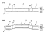
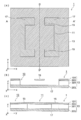
最初に、本発明における平行移動機構の第1の実施の形態について、図1および図2を用いて説明する、図1は、本発明における平行移動機構の第1の実施の形態の構成を示す模式図で、図1(a)は平面図、図1(b)は図1(a)のA-A’断面図、図1(c)は図1(a)のB-B’断面図である。図2は、本発明における平行移動機構の第1の実施の形態の動作を示す模式図で、図2(a)は動作前の状態を、図2(b)は動作後の状態を示す。
図1(a)において、図の左から右をx方向、下から上をy方向、紙面奥から手前をz方向とする。平行移動機構1は、移動部11、支持部13、2本の第1の梁15および4本の第2の梁17等で構成されている。支持部13は移動部11を囲むように配置されており、移動部11と支持部13とは、図示したように、移動部11のy方向の対向する2辺のそれぞれに設けられた2本の第1の梁15で連結されており、また、図1(b)に示すように、図の裏面側で、第1の梁15のx方向両側に設けられた4本の第2の梁17で連結されている。
図1(b)および(c)において、移動部11および支持部13は、第1の層101、中間層301および第2の層201の平行平板状の3層が積層されて構成されている。第1の層101、中間層301および第2の層201は、例えばシリコン(Si)であり、中間層301の第1の層101および第2の層201との界面は、第1の酸化膜(SiO2)303および第2の酸化膜(SiO2)305となっている。第1の層101と第2の層201との厚さは等しい。
一方、第1の梁15は第1の層101のみで構成され、第2の梁17は第2の層201のみで構成されている。従って、移動部11と支持部13とは、上面側を第1の層101で構成される第1の梁15で連結され、下面側を第2の層201で構成される第2の梁17で連結されていることになる。
第1の梁15と第2の梁17とは長さと厚さとが等しく、第1の梁15の幅が第2の梁17の2倍になっており、1本の第1の梁15と2本の第2の梁17とで曲げ剛性が等しくなるように構成されている。また、第1の梁15と第2の梁17とはx方向およびy方向に軸対称な形状となっており、平行移動機構1全体として、z方向の変形に対する剛性が等しく構成されている。
なお、図1の例では、支持部13は移動部11を囲むように配置されているとしたが、これは必須ではなく、少なくとも、第1の梁15および第2の梁17で移動部11と連結される部分があればよい。
図2は、図1(c)と同じB-B’断面図に、便宜上、第1の梁15を破線で示したものである。図2(a)の状態に対して、移動部11に外部からz方向の駆動力Fが印加されると、図2(b)に示すように、第1の梁15および第2の梁17がS字状に変形する。
上述したように、平行移動機構1全体としてz方向の変形に対する剛性が等しく構成されているので、z方向の駆動力Fに押されて、移動部11はz方向に平行移動される。外部から重力や慣性力等意図しない力が加わっても、移動部11の平行は保持される。駆動力Fとしては、図6以降で後述する電磁力や、圧電素子、形状記憶合金等による電気機械変換による力等を用いることができる。
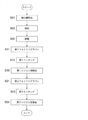
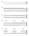
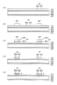
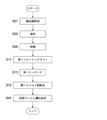
次に、上述した第1の実施の形態の製造方法について、図3、図4および図5を用いて説明する。図3は、第1の実施の形態の製造方法を示す工程図であり、図4および図5は図3の各工程を示す図1(a)のA-A’断面図である。
以下に、図4および図5を参照しながら、図3の各工程について説明する。
ステップS01(酸化膜形成工程)
図4(a)に示すように、肉厚のシリコン(Si)の平行平板からなる中間層301を高温処理することで、中間層301の片面に第1の酸化膜(SiO2)303を、他方の面に第2の酸化膜(SiO2)305を形成する。中間層301の厚さは、平行移動機構1に要求される平面性や質量等の仕様によるが、一般的には300~500μm程度である。また第1の酸化膜303および第2の酸化膜305の厚さは、後述するエッチング工程により決まるが、一般的には1μm以下である。
図4(a)に示すように、肉厚のシリコン(Si)の平行平板からなる中間層301を高温処理することで、中間層301の片面に第1の酸化膜(SiO2)303を、他方の面に第2の酸化膜(SiO2)305を形成する。中間層301の厚さは、平行移動機構1に要求される平面性や質量等の仕様によるが、一般的には300~500μm程度である。また第1の酸化膜303および第2の酸化膜305の厚さは、後述するエッチング工程により決まるが、一般的には1μm以下である。
ステップS03(接合工程)
図4(b)に示すように、第1の酸化膜303の上にシリコン(Si)の薄板101を、第2の酸化膜305の上にシリコン(Si)の薄板201を接合する。接合は、表面をプラズマ等で清浄、活性化して接合する常温接合や、電界を用いる陽極接合等により可能である。
図4(b)に示すように、第1の酸化膜303の上にシリコン(Si)の薄板101を、第2の酸化膜305の上にシリコン(Si)の薄板201を接合する。接合は、表面をプラズマ等で清浄、活性化して接合する常温接合や、電界を用いる陽極接合等により可能である。
ステップS05(研磨工程)
図4(c)に示すように、ステップS03で接合された薄板101および薄板201を薄く研磨する。研磨された薄板101および薄板201の厚みは、第1の梁15および第2の梁17に要求される剛性によって決まるが、一般的には数μm程度である。研磨によって、薄板101および薄板201から、第1の層101および第2の層201が形成される。
図4(c)に示すように、ステップS03で接合された薄板101および薄板201を薄く研磨する。研磨された薄板101および薄板201の厚みは、第1の梁15および第2の梁17に要求される剛性によって決まるが、一般的には数μm程度である。研磨によって、薄板101および薄板201から、第1の層101および第2の層201が形成される。
以上の手法は、SOI(Silicon On Insulator)基板と呼ばれる基板を作成する工程と同じで、一般に用いられるものである。SOI基板を作成する工程は、他にも複数提案されているので、それらを用いてもよい。
ステップS11(第1フォトリソグラフィ工程)
図4(d)に示すように、第1の層101の上にレジスト剤を塗布し、露光、現像等のフォトリソグラフィ工程を経ることで、次の第1エッチング工程で残したい部分にマスクパターン401を形成する。
図4(d)に示すように、第1の層101の上にレジスト剤を塗布し、露光、現像等のフォトリソグラフィ工程を経ることで、次の第1エッチング工程で残したい部分にマスクパターン401を形成する。
ステップS13(第1エッチング工程)
図4(e)に示すように、エッチングにより、マスクパターン401が形成された部分以外の、第1の層101、第1の酸化膜303、中間層301および第2の酸化膜305を除去し、第2の層201だけを残す。シリコンと酸化物とではエッチングする反応材料および速度が大きく異なるため、時間を制御することで、エッチング深さを制御することができる。あるいは、第1の層101、第1の酸化膜303、中間層301を除去し、第2の酸化膜305と第2の層201を残してもよい。
図4(e)に示すように、エッチングにより、マスクパターン401が形成された部分以外の、第1の層101、第1の酸化膜303、中間層301および第2の酸化膜305を除去し、第2の層201だけを残す。シリコンと酸化物とではエッチングする反応材料および速度が大きく異なるため、時間を制御することで、エッチング深さを制御することができる。あるいは、第1の層101、第1の酸化膜303、中間層301を除去し、第2の酸化膜305と第2の層201を残してもよい。
ステップS15(第1レジスト剤除去工程)
図5(a)に示すように、第1の層101の上に残ったレジスト剤(マスクパターン)401を除去する。
図5(a)に示すように、第1の層101の上に残ったレジスト剤(マスクパターン)401を除去する。
ステップS21(第2フォトリソグラフィ工程)
図5(b)に示すように、第2の層201の上にレジスト剤を塗布し、露光、現像等のフォトリソグラフィ工程を経ることで、次の第2エッチング工程で残したい部分にマスクパターン403を形成する。
図5(b)に示すように、第2の層201の上にレジスト剤を塗布し、露光、現像等のフォトリソグラフィ工程を経ることで、次の第2エッチング工程で残したい部分にマスクパターン403を形成する。
ステップS23(第2エッチング工程)
図5(c)に示すように、エッチングにより、マスクパターン403が形成された部分以外の、第2の層201、第2の酸化膜305、中間層301および第1の酸化膜303を除去し、第1の層101だけを残す。あるいは、第2の層201、第2の酸化膜305、中間層301を除去し、第1の酸化膜303と第1の層101を残してもよい。ステップS13と同様に、エッチング時間を制御することで、エッチング深さを制御する。
図5(c)に示すように、エッチングにより、マスクパターン403が形成された部分以外の、第2の層201、第2の酸化膜305、中間層301および第1の酸化膜303を除去し、第1の層101だけを残す。あるいは、第2の層201、第2の酸化膜305、中間層301を除去し、第1の酸化膜303と第1の層101を残してもよい。ステップS13と同様に、エッチング時間を制御することで、エッチング深さを制御する。
ステップS25(第2レジスト剤除去工程)
図5(d)に示すように、第2の層201の上に残ったレジスト剤(マスクパターン)403を除去する。
図5(d)に示すように、第2の層201の上に残ったレジスト剤(マスクパターン)403を除去する。
以上の工程によって、第1の層101のみで形成される第1の梁15と第2の層201のみで形成される第2の梁17とが残り、図1(b)に示したと同じ平行移動機構1が形成される。
上述したように、第1の実施の形態によれば、中間層の上面に第1の層が積層され、下面に第2の層が積層されて形成された移動部を、同様に形成された支持部に、第1の層で形成された第1の梁と、第2の層で形成された第2の梁とで連結して、移動部が第1の層、中間層および第2の層の積層方向に平行移動可能に構成することで、微小量の高精度な平行移動が可能な平行移動機構および平行移動機構の製造方法を提供することができる。
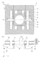
次に、第1の実施の形態の第1の応用例について、図6を用いて説明する。図6は、第1の実施の形態の第1の応用例を示す模式図で、図6(a)は図1(a)の裏面側から見た平面図、図6(b)は図6(a)のC-C’断面図である。
図6(a)および(b)において、第1の応用例では、図1(a)の移動部11の中央に、第1の層101から第2の層201までを貫通する穴が設けられ、その中に、光軸21aをz方向に向けて、レンズ21が挿入されている。
移動部11の第2の層201上には、ループ状の配線31が設けられ、配線31に対向する位置には永久磁石33が設けられている。支持部13および永久磁石33は、例えばカメラ本体の一部である固定部35に、接着等によって固定されている。配線31に通電すると、配線31に流れる電流Iと永久磁石33による磁界との作用により駆動力Fを発生させることができる。
図の例では、図6(a)の反時計回りに電流Iが流れることで、z方向の負の方向にレンズ21を移動させる駆動力Fを発生させることができる。電流Iの向きを反転させれば、z方向の正の方向にレンズ21を移動させる駆動力Fを発生させることができる。移動部11は、平行移動機構1によってz方向に平行移動するので、レンズ21もz方向即ち光軸21a方向に平行移動する。
上述したように、第1の応用例によれば、第1の実施の形態の平行移動機構をカメラレンズのピント調節やズーム機構に応用することが可能となる。
次に、第1の実施の形態の第2の応用例について、図7を用いて説明する。図7は、第1の実施の形態の第2の応用例を示す模式図で、図7(a)は図1(a)と同じ側から見た平面図、図7(b)および図7(c)は図7(a)のD-D’断面図である。
図7(a)および(b)において、第2の応用例では、図1(a)の移動部11の第1の層101の上に、例えば銀(Ag)やアルミ(Al)を蒸着して、ミラー23を形成している。
また、2個の第1の梁15の第1の層101の上に、それぞれ、2層の電極503に挟まれたPZT(チタン酸ジルコン酸鉛)等の圧電素子501からなる駆動素子51が、例えばスパッタ法等で成膜されて形成されている。所謂ユニモルフ構造である。製造方法の詳細は、図8以降で詳述する。
図7(b)の状態に対して、駆動素子51の2層の電極503の間に電界が印加されると、図7(c)に示すように、圧電素子501が、例えば電界方向即ち図のz方向に伸張し、図のy方向に収縮する。駆動素子51と第1の梁15の第1の層101とは密着しているので、圧電素子501がy方向に収縮することで、バイメタルと同様に第1の梁15がz方向に屈曲し、移動部11が支持部13に対してz方向の正方向に平行移動する。
これによって、ミラーを精密駆動する必要のある光スイッチや光干渉計への応用が可能となる。
次に、第1の実施の形態の第2の応用例の製造方法を、図8、図9および図10を用いて説明する。図8は、第1の実施の形態の第2の応用例の製造方法を示す工程図であり、図9は、図8のサブルーチンを示す工程図、図10は、図9(b)の各工程を示す図7のD-D’断面図である。
図8において、第2の応用例の工程図が図3の第1の実施の形態の工程図と異なる点は、ステップS05(研磨工程)とステップS11(第1フォトリソグラフィ工程)との間に、ステップS07(駆動素子形成サブルーチン)とステップS09(ミラー形成サブルーチン)が付加された点である。
ステップS07(駆動素子形成サブルーチン)では、2層の電極503に挟まれた圧電素子501からなる駆動素子51が形成される。詳細は図9(a)および図10に示す。
図9(a)において、ステップS31(駆動素子層形成工程)で、図10(a)に示すように、第1の層101の上に電極503、圧電素子501およびもう1層の電極503を、スパッタ等の方法でこの順に成膜して、駆動素子層51を形成する。
ステップS33(第3フォトリソグラフィ工程)で、図10(b)に示すように、駆動素子層51の上にレジスト剤を塗布し、露光、現像等のフォトリソグラフィ工程を経ることで、駆動素子51を形成したい部分にマスクパターン407を残す。
ステップS35(第3エッチング工程)で、図10(c)に示すように、エッチングにより、マスクパターン407が形成された部分以外の、電極503、圧電素子501およびもう1層の電極503を除去する。
ステップS37(第3レジスト剤除去工程)で、図10(d)に示すように、駆動素子51の上に残ったレジスト剤(マスクパターン)407を除去する。
ステップS39(分極工程)で、2層の電極503の間に高電圧を印加する等の方法により、図10(e)に示すように、駆動素子51の圧電素子501の分極Pの方向を揃える分極処理を施す。これによって、圧電素子501が駆動素子としての機能を果たすようになる。なお、分極処理は、図8のステップS25(第2レジスト剤除去工程)終了後に行ってもよい。また、スパッタ法で圧電素子501を形成する場合には、成膜時に分極が起こる。その場合には、ステップS39(分極工程)は省略できる。
続いて、ステップS09(ミラー形成サブルーチン)では、ミラー23が、例えば蒸着等の方法で形成される。詳細は図9(b)に示す。
図9(b)において、ステップS41(第4フォトリソグラフィ工程)で、第1の層101および駆動素子51の上にレジスト剤を塗布し、露光、現像等のフォトリソグラフィ工程を経ることで、ミラー23を形成したい部分に開口を有するマスクパターンを形成する。ステップS43(ミラー蒸着工程)で、ステップS41で形成されたマスクパターン上に、例えば銀(Ag)やアルミ(Al)を蒸着する。ステップS45(第4レジスト剤除去工程)で、残されたレジスト剤即ちマスクパターンを除去し、ミラー23が完成する。
以降の工程は、図3の第1の実施の形態の工程図に示したステップS11からS25と同じである。ただし、ステップS11(第1フォトリソグラフィ工程)で移動部11となる部分の第1の層101の上に形成されたマスクパターン401は、上述したミラー23の上に形成されることになる。以上の工程を経て、図7(a)および(b)に示した第1の実施の形態の第2の応用例が完成される。
上述したように、第2の応用例によれば、駆動力を発生させる部材である駆動素子51および光学的な機能部材であるミラー23を平行移動機構1の上に作りこむことができ、ミラーを精密駆動する必要のある光スイッチや光干渉計への応用が可能となるとともに、平行移動機構1の小型化、低コスト化が実現できる。
次に、第1の実施の形態の第3の応用例について、図11を用いて説明する。図11は、第1の実施の形態の第3の応用例を示す模式図で、図11(a)は図1(a)と同じ側から見た平面図、図11(b)は図11(a)のA-A’断面図、図11(c)は図11(a)のB-B’断面図である。図11(c)には、便宜上、第1の梁15も破線で記載してある。
図11(a)において、平行移動機構1は、図1(a)と同様に、移動部11、支持部13、2本の第1の梁15および4本の第2の梁17等で構成されている。支持部13は移動部11を囲むように配置されている。移動部11の上には、第2の応用例と同様に、ミラー23が蒸着等により形成されている。
2本の第1の梁15は、移動部11のy方向の対向する2箇所の一部の上面と、それに対向する支持部13の一部の上面とに跨るように設けられ、移動部11と支持部13とを連結している。
また、4本の第2の梁17も、破線で示したように、図の裏面側で、第1の梁15のx方向両側に、移動部11の一部の上面と、それに対向する支持部13の一部の上面とに跨るように設けられ、移動部11と支持部13とを連結している。
2本の第1の梁15の上には、それぞれ、形状記憶合金のループ状の配線53が、例えばスパッタ等の方法で形成されている。
図11(b)および(c)において、移動部11および支持部13は、例えばシリコン(Si)からなる中間層301の両面に、第1の酸化膜(SiO2)303および第2の酸化膜(SiO2)305が形成されて構成されている。
一方、第1の梁15は第1の層101のみで構成され、移動部11の一部の上面と、それに対向する支持部13の一部の上面とに跨るように設けられている。第1の梁15の上には、形状記憶合金のループ状の配線53が形成されている。また、第2の梁17は第2の層201のみで構成され、移動部11の一部の下面と、それに対向する支持部13の一部の下面とに跨るように設けられている。
上述したように、第1の層101は、第1の梁15として移動部11と支持部13とを連結し、第2の層201は、第2の梁17として移動部11と支持部13とを連結している。そして、第1の梁15の上には、駆動素子としての形状記憶合金のループ状の配線53が形成されている。
第1の梁15と第2の梁17とは長さと厚さとが等しく、第1の梁15の幅が第2の梁17の2倍になっており、1本の第1の梁15と2本の第2の梁17とで曲げ剛性が等しくなるように構成されている。また、第1の梁15と第2の梁17とはx方向およびy方向に軸対称な形状となっており、平行移動機構1全体として、z方向の変形に対する剛性が等しく構成されている。
形状記憶合金のループ状の配線53には予め高温でy方向に収縮する特性が記憶させてあり、形状記憶合金のループ状の配線53に通電することで、ジュール熱により自身が発熱して高温となり、y方向に収縮する。従って、第2の応用例と同様に第1の梁15がz方向に屈曲し、移動部11が支持部13に対してz方向の正方向に平行移動する。
第3の応用例の製造方法は、図8および図9に示した第2の応用例の製造方法とほぼ同様であるので、説明は省略する。ただし、形状記憶合金のループ状の配線53に形状を記憶させる形状記憶工程は、図9(a)のステップS39(分極工程)に相当する工程ではなく、図8のステップS25(第2レジスト剤除去工程)の終了後に設ける必要がある。
上述したように、第3の応用例によれば、第2の応用例と同様に、駆動力を発生させる部材である駆動素子51および光学的な機能部材であるミラー23を平行移動機構1の上に作りこむことができ、ミラーを精密駆動する必要のある光スイッチや光干渉計への応用が可能となるとともに、平行移動機構1の小型化、低コスト化が実現できる。
次に、本発明における平行移動機構の第2の実施の形態の形状について、図12を用いて説明する。図12は、第2の実施の形態の構成を示す模式図で、図12(a)は平面図、図12(b)は図12(a)のA-A’断面図、図12(c)は図1(a)のD-D’断面図である。
図12(a)において、図1(a)と同様に、平行移動機構1は、移動部11、支持部13、2本の第1の梁15および第2の梁17等で構成されている。支持部13は移動部11を囲むように配置されており、移動部11と支持部13とは、図示したように、移動部11のy方向の対向する2辺のそれぞれに設けられた2本の第1の梁15で連結されており、また、図12(c)に示すように、図の裏面側の全面に設けられた第2の梁17で連結されている。
図12(b)および(c)において、移動部11および支持部13は、第1の層101、中間層301および樹脂フィルム層203の平行平板状の3層が積層されて構成されている。第1の層101および中間層301は、例えばシリコン(Si)であり、中間層301の第1の層101との界面は、第1の酸化膜(SiO2)303となっている。
一方、第1の梁15は第1の層101のみで構成され、第2の梁17は樹脂フィルム層203のみで構成されている。従って、移動部11と支持部13とは、上面側を第1の層101で構成される第1の梁15で連結され、下面側を樹脂フィルム層203で構成される第2の梁17で連結されていることになる。
樹脂フィルム層203は伸縮性が高いため、形状加工を施さなくても梁の機能を果たすことができる。第2の梁17だけでなく、第1の梁15についても、樹脂フィルム層としても構成が可能である。
また、中間層301の樹脂フィルム層203との界面についても、第1の実施の形態と同様に、第2の酸化膜(SiO2)305としてもよい。
続いて、第2の実施の形態の製造方法について、図13および図14を用いて説明する。図13は、第2の実施の形態の製造方法を示す工程図であり、図14は、図13の各工程を示す図12(a)のD-D’断面図である。
図13において、ステップS01(酸化膜形成工程)からステップS15(第1レジスト剤除去工程)までは、図3の第1の実施の形態の製造方法の工程図とほぼ同様である。
ただし、第1の実施の形態では、中間層301の両面に、第1の酸化膜(SiO2)303および第2の酸化膜(SiO2)305と、第1の層101および第2の層201を形成し、第1の層101の側と第2の層201の側とからエッチングを行うことで、平行移動機構1を形成した。
それに対して、第2の実施の形態では、図14(a)、(b)および(c)に示すように、中間層301の上面に第1の酸化膜(SiO2)303を形成し、その上にシリコン(Si)の薄板101を接合して研磨することで、第1の層101を形成する。そして、図14(d)、(e)および(f)に示すように、中間層301の第1の層101とは反対の側からエッチングを行うことで、移動部11、支持部13および第1の梁15を形成する。
次に、図13のステップS41(樹脂フィルム層貼合せ工程)で、図14(g)に示すように、中間層301の第1の層101とは反対の面に、接着等の方法により、樹脂フィルム層203をベタで貼り付けて第2の梁17とし、平行移動機構1が完成される。
上述したように、第2の実施の形態によれば、伸縮性の高い樹脂フィルム層203を用いることで、形状加工を施さなくても第2の梁17としての機能を果たすことができるので、第2の梁17を形成するための工程を簡略化することができ、製造コストの低減にも寄与できる。第1の梁15も樹脂フィルム化すれば、さらに工程の簡略化と製造コストの低減が行える。
次に、本発明における平行移動機構の第3の実施の形態の形状について、図15を用いて説明する。図15は、第3の実施の形態の構成を示す断面模式図で、図15(a)は動作前の状態を、図15(b)は動作後の状態を示す。
図15(a)において、第3の実施の形態では、上述した第1および第2の実施の形態とは異なり、1対の移動部11と支持部13とが、1対の第1の梁15と第2の梁17とで連結されている。
移動部11および支持部13は、第1の層101、中間層301および第2の層201の平行平板状の3層が積層されて構成されている。第1の層101、中間層301および第2の層201は、例えばシリコン(Si)であり、中間層301の第1の層101との界面は、第1の酸化膜(SiO2)303となっている。
一方、第1の梁15は第1の層101のみで構成され、第2の梁17は第2の層201のみで構成されている。
図15(a)の状態に対して、移動部11に外部からz方向の駆動力Fが印加されると、図15(b)に示すように、第1の梁15および第2の梁17がS字状に変形し、移動
部11がz方向に平行移動される。外部から重力や慣性力等意図しない力が加わっても、移動部11の平行は保持される。駆動力Fとしては、図6以降で述べた電磁力や、圧電素子、形状記憶合金等による電気機械変換による力等を用いることができる。
部11がz方向に平行移動される。外部から重力や慣性力等意図しない力が加わっても、移動部11の平行は保持される。駆動力Fとしては、図6以降で述べた電磁力や、圧電素子、形状記憶合金等による電気機械変換による力等を用いることができる。
上述したように、第3の実施の形態によれば、機構の構成が簡単で、小型化に適しており、コスト的にも安価に製造できる。また、梁のy方向の引っ張り合いがないので、z方向の変位が大きくなるなどのメリットがある。ただし、移動部11のz方向への移動時に、y方向への変位が生じるので、例えば図6に示した第1の実施の形態の第1の応用例のようなレンズ21の駆動等のy方向への変位が許容されないものには使用できない。
次に、上述した各実施の形態および応用例の梁の形状の改良案について、図16を用いて説明する。図16は、梁の形状の改良案を示す模式図で、図16(a)は上述した各実施の形態および応用例に示した梁の形状を、図16(b)は改良された梁の形状の1例を示す。
SOI基板を用いた平行移動機構1における梁は、両端が変形しやすく、中央は変形しにくい性質である方が、通常の機械的なリンク機構に近く、望ましい。そこで、移動部11と支持部13とを連結する第1の梁15あるいは第2の梁17において、図16(a)に示したような均一な幅の梁形状ではなく、図16(b)に示したような梁の両端部分に切り欠き部19を設けた形状とする。
上述したように、梁の形状の改良案によれば、梁の両端の剛性を下げて変形しやすくでき、両端が変形しやすく、中央は変形しにくい性質を持たせることができ、通常の機械的なリンク機構に近い平行移動機構を実現することができる。
以上に述べたように、本発明によれば、中間層の上面に第1の層が積層され、下面に第2の層が積層されて形成された移動部を、同様に形成された支持部に、第1の層で形成された第1の梁と、第2の層で形成された第2の梁とで連結して、移動部が第1の層、中間層および第2の層の積層方向に平行移動可能に構成することで、光学部品の傾きや位置ズレを抑制でき、微小量の高精度な平行移動が可能で、小さな駆動力で大きな変位を得ることができる平行移動機構および平行移動機構の製造方法を提供することができる。
なお、本発明に係る平行移動機構および平行移動機構の製造方法を構成する各構成の細部構成および細部動作に関しては、本発明の趣旨を逸脱することのない範囲で適宜変更可能である。
1 平行移動機構
11 移動部
13 支持部
15 第1の梁
17 第2の梁
19 (梁の)切り欠き部
21 レンズ
21a 光軸
23 ミラー
31 ループ状の配線
33 永久磁石
35 固定部
51 駆動素子
53 形状記憶合金のループ状の配線
101 第1の層
201 第2の層
203 樹脂フィルム層
301 中間層
303 第1の酸化膜
305 第2の酸化膜
401 マスクパターン
403 マスクパターン
407 マスクパターン
501 圧電素子
503 電極
11 移動部
13 支持部
15 第1の梁
17 第2の梁
19 (梁の)切り欠き部
21 レンズ
21a 光軸
23 ミラー
31 ループ状の配線
33 永久磁石
35 固定部
51 駆動素子
53 形状記憶合金のループ状の配線
101 第1の層
201 第2の層
203 樹脂フィルム層
301 中間層
303 第1の酸化膜
305 第2の酸化膜
401 マスクパターン
403 マスクパターン
407 マスクパターン
501 圧電素子
503 電極
Claims (8)
- 中間層の上面の少なくとも一部に第1の層が積層されるとともに、前記中間層の下面の少なくとも一部に第2の層が積層されて形成された移動部と、
前記中間層の上面の少なくとも一部に前記第1の層が積層されるとともに、前記中間層の下面の少なくとも一部に前記第2の層が積層されて形成され、少なくとも前記移動部に対向する位置に設けられた支持部と、
前記移動部の前記第1の層と、前記移動部の前記第1の層に対向する前記支持部の前記第1の層とを連結する前記第1の層で形成された第1の梁と、
前記移動部の前記第2の層と、前記移動部の前記第2の層に対向する前記支持部の前記第2の層とを連結する前記第2の層で形成された第2の梁とを備え、
前記移動部が前記第1の層、前記中間層および前記第2の層の積層方向に平行移動可能であることを特徴とする平行移動機構。 - 前記支持部は、少なくとも前記移動部を挟む位置に設けられ、
前記第1の梁は、少なくとも2本設けられ、前記移動部の前記第1の層と、前記移動部の前記第1の層に対向する前記支持部の前記第1の層とを連結し、
前記第2の梁は、少なくとも2本設けられ、前記移動部の前記第2の層と、前記移動部の前記第2の層に対向する前記支持部の前記第2の層とを連結することを特徴とする請求項1に記載の平行移動機構。 - 前記第1の層、前記中間層および前記第2の層は、SOI(Silicon On Insulator)基板であることを特徴とする請求項1または2に記載の平行移動機構。
- 前記第1の層および前記第2の層の少なくとも一方が、樹脂フィルムであることを特徴とする請求項1または2に記載の平行移動機構。
- 前記移動部の一方の平面の上に、光を反射するミラー層を形成したことを特徴とする請求項1から4の何れか1項に記載の平行移動機構。
- 前記移動部は、前記移動部を形成する各層の積層方向に貫通する開口部を有し、
前記開口部に、前記積層方向に光軸を向けてレンズを挿入したことを特徴とする請求項1から4の何れか1項に記載の平行移動機構。 - 前記移動部の一方の平面の上に、前記移動部を前記第1の層、前記中間層および前記第2の層の積層方向に平行移動させるための駆動層を設けたことを特徴とする請求項1から6の何れか1項に記載の平行移動機構。
- シリコンの平行平板からなる中間層の、対向する表面の一方に第1の酸化膜を形成し、他方に第2の酸化膜を形成する酸化膜形成工程と、
前記第1の酸化膜の上に第1のシリコンの平行平板を接合し、前記第2の酸化膜の上に第2のシリコンの平行平板を接合する接合工程と、
接合された前記第1のシリコンの平行平板を研磨して第1の層を形成し、前記第2のシリコンの平行平板を研磨して第2の層を形成する研磨工程と、
前記第1の層の上にレジスト剤を塗布し、フォトリソグラフィ法により、移動部となる部分、支持部となる部分、および、前記第1の層で構成され、前記移動部と前記支持部とを連結する第1の梁となる部分にマスクパターンを形成する第1フォトリソグラフィ工程と、
エッチングにより、前記第1の層、前記第1の酸化膜および前記中間層の、前記移動部、前記支持部および前記第1の梁以外の部分を除去する第1エッチング工程と、
前記第1の層の上に残ったレジスト剤を除去する第1レジスト剤除去工程と、
前記第2の層の上にレジスト剤を塗布し、フォトリソグラフィ法により、移動部となる部分、支持部となる部分、および、前記第2の層で構成され、前記移動部と前記支持部とを連結する第2の梁となる部分にマスクパターンを形成する第2フォトリソグラフィ工程と、
エッチングにより、前記第2の層、前記第2の酸化膜および前記中間層の、前記移動部、前記支持部および前記第2の梁以外の部分を除去する第2エッチング工程と、
前記第2の層の上に残ったレジスト剤を除去する第2レジスト剤除去工程とを、この順に行うことを特徴とする平行移動機構の製造方法。
Priority Applications (1)
| Application Number | Priority Date | Filing Date | Title |
|---|---|---|---|
| JP2011502707A JP5354006B2 (ja) | 2009-03-04 | 2010-02-18 | 平行移動機構および平行移動機構の製造方法 |
Applications Claiming Priority (2)
| Application Number | Priority Date | Filing Date | Title |
|---|---|---|---|
| JP2009050577 | 2009-03-04 | ||
| JP2009-050577 | 2009-03-04 |
Publications (1)
| Publication Number | Publication Date |
|---|---|
| WO2010101023A1 true WO2010101023A1 (ja) | 2010-09-10 |
Family
ID=42709584
Family Applications (1)
| Application Number | Title | Priority Date | Filing Date |
|---|---|---|---|
| PCT/JP2010/052423 Ceased WO2010101023A1 (ja) | 2009-03-04 | 2010-02-18 | 平行移動機構および平行移動機構の製造方法 |
Country Status (2)
| Country | Link |
|---|---|
| JP (1) | JP5354006B2 (ja) |
| WO (1) | WO2010101023A1 (ja) |
Cited By (1)
| Publication number | Priority date | Publication date | Assignee | Title |
|---|---|---|---|---|
| JP2016521864A (ja) * | 2013-05-27 | 2016-07-25 | フラウンホーファー−ゲゼルシャフト・ツール・フェルデルング・デル・アンゲヴァンテン・フォルシュング・アインゲトラーゲネル・フェライン | 橋渡し部材を備える光学構造およびその製造方法 |
Citations (7)
| Publication number | Priority date | Publication date | Assignee | Title |
|---|---|---|---|---|
| GB2194341A (en) * | 1986-07-26 | 1988-03-02 | Messerschmitt Boelkow Blohm | Capacitive acceleration sensors |
| DE19603829A1 (de) * | 1996-02-02 | 1997-08-07 | Daimler Benz Ag | Verfahren zur Herstellung von mikromechanischen Strukturen aus Silizium |
| JP3037416B2 (ja) * | 1990-07-14 | 2000-04-24 | ローベルト ボツシユ ゲゼルシヤフト ミツト ベシユレンクテル ハフツング | マイクロメカニック式の回転値センサ |
| JP2000330067A (ja) * | 1999-05-20 | 2000-11-30 | Olympus Optical Co Ltd | ねじり揺動体 |
| US20040027225A1 (en) * | 2002-08-09 | 2004-02-12 | Hsiao-Wen Lee | Micro electromechanical differential actuator |
| JP2006072251A (ja) * | 2004-09-06 | 2006-03-16 | Nippon Signal Co Ltd:The | プレーナ型アクチュエータ |
| JP2010046730A (ja) * | 2008-08-20 | 2010-03-04 | Nippon Telegr & Teleph Corp <Ntt> | 微細構造体 |
Family Cites Families (4)
| Publication number | Priority date | Publication date | Assignee | Title |
|---|---|---|---|---|
| JPH0832090A (ja) * | 1994-07-12 | 1996-02-02 | Mitsubishi Electric Corp | 慣性力センサおよびその製造方法 |
| FR2735580B1 (fr) * | 1995-06-14 | 1997-07-18 | Commissariat Energie Atomique | Accelerometre du type a compensation de l'effet de la pesanteur et procede de realisation d'un tel accelerometre |
| JP2924738B2 (ja) * | 1995-09-29 | 1999-07-26 | オムロン株式会社 | 光偏向装置 |
| JP4783558B2 (ja) * | 2003-07-22 | 2011-09-28 | 日本碍子株式会社 | アクチュエータ装置 |
-
2010
- 2010-02-18 JP JP2011502707A patent/JP5354006B2/ja not_active Expired - Fee Related
- 2010-02-18 WO PCT/JP2010/052423 patent/WO2010101023A1/ja not_active Ceased
Patent Citations (7)
| Publication number | Priority date | Publication date | Assignee | Title |
|---|---|---|---|---|
| GB2194341A (en) * | 1986-07-26 | 1988-03-02 | Messerschmitt Boelkow Blohm | Capacitive acceleration sensors |
| JP3037416B2 (ja) * | 1990-07-14 | 2000-04-24 | ローベルト ボツシユ ゲゼルシヤフト ミツト ベシユレンクテル ハフツング | マイクロメカニック式の回転値センサ |
| DE19603829A1 (de) * | 1996-02-02 | 1997-08-07 | Daimler Benz Ag | Verfahren zur Herstellung von mikromechanischen Strukturen aus Silizium |
| JP2000330067A (ja) * | 1999-05-20 | 2000-11-30 | Olympus Optical Co Ltd | ねじり揺動体 |
| US20040027225A1 (en) * | 2002-08-09 | 2004-02-12 | Hsiao-Wen Lee | Micro electromechanical differential actuator |
| JP2006072251A (ja) * | 2004-09-06 | 2006-03-16 | Nippon Signal Co Ltd:The | プレーナ型アクチュエータ |
| JP2010046730A (ja) * | 2008-08-20 | 2010-03-04 | Nippon Telegr & Teleph Corp <Ntt> | 微細構造体 |
Cited By (2)
| Publication number | Priority date | Publication date | Assignee | Title |
|---|---|---|---|---|
| JP2016521864A (ja) * | 2013-05-27 | 2016-07-25 | フラウンホーファー−ゲゼルシャフト・ツール・フェルデルング・デル・アンゲヴァンテン・フォルシュング・アインゲトラーゲネル・フェライン | 橋渡し部材を備える光学構造およびその製造方法 |
| US10571646B2 (en) | 2013-05-27 | 2020-02-25 | Fraunhofer-Gesellschaft Zur Foerderung Der Angewandten Forschung E.V. | Optical structure with ridges arranged at the same and method for producing the same |
Also Published As
| Publication number | Publication date |
|---|---|
| JP5354006B2 (ja) | 2013-11-27 |
| JPWO2010101023A1 (ja) | 2012-09-06 |
Similar Documents
| Publication | Publication Date | Title |
|---|---|---|
| CN212723526U (zh) | Mems致动器 | |
| JP4335114B2 (ja) | マイクロミラーデバイス | |
| US7952778B2 (en) | Biaxial MEMS mirror with hidden hinge | |
| CN101284642A (zh) | 具有倾斜电极的微机械器件 | |
| JP6390508B2 (ja) | 光走査装置 | |
| JP5694007B2 (ja) | Mems揺動装置 | |
| JP4193817B2 (ja) | アクチュエータ | |
| CN101137923A (zh) | 微小机械构造体 | |
| JP5354006B2 (ja) | 平行移動機構および平行移動機構の製造方法 | |
| US7261430B1 (en) | Thermal and intrinsic stress compensated micromirror apparatus and method | |
| JP7105934B2 (ja) | Memsミラー装置及びその製造方法 | |
| US6894819B2 (en) | Micromirror actuator and method of manufacturing the same | |
| US9244269B2 (en) | Micro movable device and optical switching apparatus | |
| JP6216485B1 (ja) | 変位拡大機構及びシャッタ装置 | |
| JP5513184B2 (ja) | マイクロ構造体及びその製造方法 | |
| JP2006187060A (ja) | マイクロアクチュエータ及びその製造方法、並びに、光学装置及び光スイッチ | |
| JPWO2002103432A1 (ja) | 光スイッチ | |
| JP7713656B2 (ja) | 圧電駆動素子 | |
| CN120622403A (zh) | 一种混合驱动的mems器件及其制备方法 | |
| JP4419536B2 (ja) | 薄膜構造体の製造方法及びこれに用いられる試料 | |
| JP2004004547A (ja) | 光学装置 | |
| JP6390522B2 (ja) | 光走査装置 | |
| JP2005153057A (ja) | マイクロアクチュエータ、並びに、これを用いた光学装置及び光スイッチ | |
| JP2004133212A (ja) | 光スイッチ装置 | |
| JP2008040298A (ja) | 形状可変ミラー |
Legal Events
| Date | Code | Title | Description |
|---|---|---|---|
| 121 | Ep: the epo has been informed by wipo that ep was designated in this application |
Ref document number: 10748619 Country of ref document: EP Kind code of ref document: A1 |
|
| WWE | Wipo information: entry into national phase |
Ref document number: 2011502707 Country of ref document: JP |
|
| NENP | Non-entry into the national phase |
Ref country code: DE |
|
| 122 | Ep: pct application non-entry in european phase |
Ref document number: 10748619 Country of ref document: EP Kind code of ref document: A1 |