WO2010100861A1 - 超音波トランスデューサ、その製造方法、および、それを用いた超音波探触子 - Google Patents
超音波トランスデューサ、その製造方法、および、それを用いた超音波探触子 Download PDFInfo
- Publication number
- WO2010100861A1 WO2010100861A1 PCT/JP2010/001200 JP2010001200W WO2010100861A1 WO 2010100861 A1 WO2010100861 A1 WO 2010100861A1 JP 2010001200 W JP2010001200 W JP 2010001200W WO 2010100861 A1 WO2010100861 A1 WO 2010100861A1
- Authority
- WO
- WIPO (PCT)
- Prior art keywords
- insulating film
- ultrasonic transducer
- lower electrode
- cavity
- electrical connection
- Prior art date
- Legal status (The legal status is an assumption and is not a legal conclusion. Google has not performed a legal analysis and makes no representation as to the accuracy of the status listed.)
- Ceased
Links
Images









Classifications
-
- B—PERFORMING OPERATIONS; TRANSPORTING
- B06—GENERATING OR TRANSMITTING MECHANICAL VIBRATIONS IN GENERAL
- B06B—METHODS OR APPARATUS FOR GENERATING OR TRANSMITTING MECHANICAL VIBRATIONS OF INFRASONIC, SONIC, OR ULTRASONIC FREQUENCY, e.g. FOR PERFORMING MECHANICAL WORK IN GENERAL
- B06B1/00—Methods or apparatus for generating mechanical vibrations of infrasonic, sonic, or ultrasonic frequency
- B06B1/02—Methods or apparatus for generating mechanical vibrations of infrasonic, sonic, or ultrasonic frequency making use of electrical energy
- B06B1/0292—Electrostatic transducers, e.g. electret-type
-
- B—PERFORMING OPERATIONS; TRANSPORTING
- B81—MICROSTRUCTURAL TECHNOLOGY
- B81C—PROCESSES OR APPARATUS SPECIALLY ADAPTED FOR THE MANUFACTURE OR TREATMENT OF MICROSTRUCTURAL DEVICES OR SYSTEMS
- B81C1/00—Manufacture or treatment of devices or systems in or on a substrate
- B81C1/00015—Manufacture or treatment of devices or systems in or on a substrate for manufacturing microsystems
- B81C1/00134—Manufacture or treatment of devices or systems in or on a substrate for manufacturing microsystems comprising flexible or deformable structures
- B81C1/00182—Arrangements of deformable or non-deformable structures, e.g. membrane and cavity for use in a transducer
-
- B—PERFORMING OPERATIONS; TRANSPORTING
- B81—MICROSTRUCTURAL TECHNOLOGY
- B81C—PROCESSES OR APPARATUS SPECIALLY ADAPTED FOR THE MANUFACTURE OR TREATMENT OF MICROSTRUCTURAL DEVICES OR SYSTEMS
- B81C1/00—Manufacture or treatment of devices or systems in or on a substrate
- B81C1/00436—Shaping materials, i.e. techniques for structuring the substrate or the layers on the substrate
- B81C1/00444—Surface micromachining, i.e. structuring layers on the substrate
- B81C1/00468—Releasing structures
- B81C1/00476—Releasing structures removing a sacrificial layer
-
- B—PERFORMING OPERATIONS; TRANSPORTING
- B81—MICROSTRUCTURAL TECHNOLOGY
- B81C—PROCESSES OR APPARATUS SPECIALLY ADAPTED FOR THE MANUFACTURE OR TREATMENT OF MICROSTRUCTURAL DEVICES OR SYSTEMS
- B81C1/00—Manufacture or treatment of devices or systems in or on a substrate
- B81C1/00436—Shaping materials, i.e. techniques for structuring the substrate or the layers on the substrate
- B81C1/00555—Achieving a desired geometry, i.e. controlling etch rates, anisotropy or selectivity
- B81C1/00611—Processes for the planarisation of structures
-
- B—PERFORMING OPERATIONS; TRANSPORTING
- B81—MICROSTRUCTURAL TECHNOLOGY
- B81C—PROCESSES OR APPARATUS SPECIALLY ADAPTED FOR THE MANUFACTURE OR TREATMENT OF MICROSTRUCTURAL DEVICES OR SYSTEMS
- B81C1/00—Manufacture or treatment of devices or systems in or on a substrate
- B81C1/00015—Manufacture or treatment of devices or systems in or on a substrate for manufacturing microsystems
- B81C1/00134—Manufacture or treatment of devices or systems in or on a substrate for manufacturing microsystems comprising flexible or deformable structures
- B81C1/00158—Diaphragms, membranes
-
- B—PERFORMING OPERATIONS; TRANSPORTING
- B81—MICROSTRUCTURAL TECHNOLOGY
- B81C—PROCESSES OR APPARATUS SPECIALLY ADAPTED FOR THE MANUFACTURE OR TREATMENT OF MICROSTRUCTURAL DEVICES OR SYSTEMS
- B81C1/00—Manufacture or treatment of devices or systems in or on a substrate
- B81C1/00015—Manufacture or treatment of devices or systems in or on a substrate for manufacturing microsystems
- B81C1/00214—Processes for the simultaneaous manufacturing of a network or an array of similar microstructural devices
-
- B—PERFORMING OPERATIONS; TRANSPORTING
- B81—MICROSTRUCTURAL TECHNOLOGY
- B81C—PROCESSES OR APPARATUS SPECIALLY ADAPTED FOR THE MANUFACTURE OR TREATMENT OF MICROSTRUCTURAL DEVICES OR SYSTEMS
- B81C1/00—Manufacture or treatment of devices or systems in or on a substrate
- B81C1/00436—Shaping materials, i.e. techniques for structuring the substrate or the layers on the substrate
- B81C1/00523—Etching material
- B81C1/00531—Dry etching
-
- B—PERFORMING OPERATIONS; TRANSPORTING
- B81—MICROSTRUCTURAL TECHNOLOGY
- B81C—PROCESSES OR APPARATUS SPECIALLY ADAPTED FOR THE MANUFACTURE OR TREATMENT OF MICROSTRUCTURAL DEVICES OR SYSTEMS
- B81C2201/00—Manufacture or treatment of microstructural devices or systems
- B81C2201/01—Manufacture or treatment of microstructural devices or systems in or on a substrate
- B81C2201/0101—Shaping material; Structuring the bulk substrate or layers on the substrate; Film patterning
- B81C2201/0102—Surface micromachining
- B81C2201/0104—Chemical-mechanical polishing [CMP]
-
- B—PERFORMING OPERATIONS; TRANSPORTING
- B81—MICROSTRUCTURAL TECHNOLOGY
- B81C—PROCESSES OR APPARATUS SPECIALLY ADAPTED FOR THE MANUFACTURE OR TREATMENT OF MICROSTRUCTURAL DEVICES OR SYSTEMS
- B81C2201/00—Manufacture or treatment of microstructural devices or systems
- B81C2201/01—Manufacture or treatment of microstructural devices or systems in or on a substrate
- B81C2201/0101—Shaping material; Structuring the bulk substrate or layers on the substrate; Film patterning
- B81C2201/0102—Surface micromachining
- B81C2201/0105—Sacrificial layer
- B81C2201/0107—Sacrificial metal
-
- B—PERFORMING OPERATIONS; TRANSPORTING
- B81—MICROSTRUCTURAL TECHNOLOGY
- B81C—PROCESSES OR APPARATUS SPECIALLY ADAPTED FOR THE MANUFACTURE OR TREATMENT OF MICROSTRUCTURAL DEVICES OR SYSTEMS
- B81C2201/00—Manufacture or treatment of microstructural devices or systems
- B81C2201/01—Manufacture or treatment of microstructural devices or systems in or on a substrate
- B81C2201/0101—Shaping material; Structuring the bulk substrate or layers on the substrate; Film patterning
- B81C2201/0102—Surface micromachining
- B81C2201/0105—Sacrificial layer
- B81C2201/0109—Sacrificial layers not provided for in B81C2201/0107 - B81C2201/0108
-
- C—CHEMISTRY; METALLURGY
- C09—DYES; PAINTS; POLISHES; NATURAL RESINS; ADHESIVES; COMPOSITIONS NOT OTHERWISE PROVIDED FOR; APPLICATIONS OF MATERIALS NOT OTHERWISE PROVIDED FOR
- C09K—MATERIALS FOR MISCELLANEOUS APPLICATIONS, NOT PROVIDED FOR ELSEWHERE
- C09K13/00—Etching, surface-brightening or pickling compositions
-
- C—CHEMISTRY; METALLURGY
- C23—COATING METALLIC MATERIAL; COATING MATERIAL WITH METALLIC MATERIAL; CHEMICAL SURFACE TREATMENT; DIFFUSION TREATMENT OF METALLIC MATERIAL; COATING BY VACUUM EVAPORATION, BY SPUTTERING, BY ION IMPLANTATION OR BY CHEMICAL VAPOUR DEPOSITION, IN GENERAL; INHIBITING CORROSION OF METALLIC MATERIAL OR INCRUSTATION IN GENERAL
- C23F—NON-MECHANICAL REMOVAL OF METALLIC MATERIAL FROM SURFACE; INHIBITING CORROSION OF METALLIC MATERIAL OR INCRUSTATION IN GENERAL; MULTI-STEP PROCESSES FOR SURFACE TREATMENT OF METALLIC MATERIAL INVOLVING AT LEAST ONE PROCESS PROVIDED FOR IN CLASS C23 AND AT LEAST ONE PROCESS COVERED BY SUBCLASS C21D OR C22F OR CLASS C25
- C23F4/00—Processes for removing metallic material from surfaces, not provided for in group C23F1/00 or C23F3/00
-
- H—ELECTRICITY
- H10—SEMICONDUCTOR DEVICES; ELECTRIC SOLID-STATE DEVICES NOT OTHERWISE PROVIDED FOR
- H10D—INORGANIC ELECTRIC SEMICONDUCTOR DEVICES
- H10D48/00—Individual devices not covered by groups H10D1/00 - H10D44/00
- H10D48/50—Devices controlled by mechanical forces, e.g. pressure
-
- H—ELECTRICITY
- H10—SEMICONDUCTOR DEVICES; ELECTRIC SOLID-STATE DEVICES NOT OTHERWISE PROVIDED FOR
- H10P—GENERIC PROCESSES OR APPARATUS FOR THE MANUFACTURE OR TREATMENT OF DEVICES COVERED BY CLASS H10
- H10P50/00—Etching of wafers, substrates or parts of devices
- H10P50/60—Wet etching
- H10P50/64—Wet etching of semiconductor materials
- H10P50/642—Chemical etching
-
- Y—GENERAL TAGGING OF NEW TECHNOLOGICAL DEVELOPMENTS; GENERAL TAGGING OF CROSS-SECTIONAL TECHNOLOGIES SPANNING OVER SEVERAL SECTIONS OF THE IPC; TECHNICAL SUBJECTS COVERED BY FORMER USPC CROSS-REFERENCE ART COLLECTIONS [XRACs] AND DIGESTS
- Y10—TECHNICAL SUBJECTS COVERED BY FORMER USPC
- Y10T—TECHNICAL SUBJECTS COVERED BY FORMER US CLASSIFICATION
- Y10T29/00—Metal working
- Y10T29/49—Method of mechanical manufacture
- Y10T29/49002—Electrical device making
- Y10T29/49117—Conductor or circuit manufacturing
- Y10T29/49124—On flat or curved insulated base, e.g., printed circuit, etc.
- Y10T29/49155—Manufacturing circuit on or in base
- Y10T29/49156—Manufacturing circuit on or in base with selective destruction of conductive paths
Definitions
- the present invention relates to an ultrasonic transducer, a method for manufacturing the same, and an ultrasonic probe using the same.
- the present invention relates to an ultrasonic transducer manufactured by MEMS (Micro Electro Mechanical System) technology and an optimal manufacturing method thereof.
- MEMS Micro Electro Mechanical System
- Ultrasonic transducers are used for diagnosis of tumors in the human body and non-destructive inspection of structures by transmitting and receiving ultrasonic waves.
- CMUT Capacitive Micromachined Ultrasonic
- Patent Document 1 discloses a single CMUT and a CMUT arranged in an array.
- Patent Document 2 discloses a technique for forming a CMUT on an upper layer of a signal processing circuit formed on a silicon substrate. Yes.
- Patent Document 4 discloses a technique for supplying an electric signal to a lower electrode of a CMUT formed on a silicon substrate by providing a hole penetrating the silicon substrate.
- CMUT Compared with a conventional transducer using a piezoelectric material, CMUT has advantages such as a wide frequency band of ultrasonic waves that can be used or high sensitivity. Further, since it is manufactured using LSI processing technology, fine processing is possible. In particular, when the ultrasonic elements are arranged in an array and each element is controlled independently, CMUT is considered essential. This is because wiring to each element is required, and the number of wirings in the array may be enormous. However, since CMUT is manufactured using LSI processing technology, wiring is easy. Because. Furthermore, the CMUT can also be mounted on a single chip of the signal processing circuit from the ultrasonic transmission / reception unit.
- FIG. 22 shows a cross-sectional structure of one CMUT cell.
- a cavity 102 is formed in the upper layer of the lower electrode 101, and an insulating film 103 surrounds the cavity 102.
- An upper electrode 104 is disposed on the insulating film 103.
- the insulating film 103 and the upper electrode 104 constitute a membrane 105 that vibrates when the CMUT is driven.
- the membrane 105 vibrates due to the pressure of the ultrasonic wave that has reached the surface of the membrane 105. Then, since the distance between the upper electrode 104 and the lower electrode 101 changes, ultrasonic waves can be detected as a change in capacitance.
- the upper electrode 104 including the cavity 102 and the lower electrode 101 greatly affects ultrasonic transmission / reception characteristics. That is, when the CMUT is designed and manufactured to obtain desired transmission sound pressure and reception sensitivity, the thickness of the cavity 102 and the insulating film 103 sandwiched between the upper and lower electrodes, the unevenness of the lower electrode surface, the swelling of the membrane, It is necessary to control the dent. In particular, when a plurality of CMUT cells are arranged in an array, variations in individual cells cause variations in ultrasonic characteristics, and the designed desired transmission sound pressure and reception sensitivity cannot be obtained.
- FIG. 23 is a top view showing the positions of the lower electrode and the upper electrode when CMUTs are arranged in an array.
- FIG. 23A shows an arrangement in which CMUT arrays are arranged in a strip shape. The upper electrode is common to each strip, and the lower electrode is common to all strips, and is called a one-dimensional CMUT.
- the ultrasonic waves can be converged only in the azimuth direction by changing the transmission and reception phases in the direction in which the strips are arranged (referred to as the azimuth direction).
- FIG. 23B also divides the lower electrode of the one-dimensional CMUT of FIG. 23A, and the upper electrode and the lower electrode are arranged orthogonally.
- the ultrasonic waves can be converged not only in the azimuth direction but also in a direction orthogonal to the azimuth direction (referred to as the elevation direction), which is called a 1.5-dimensional CMUT. Since the ultrasonic wave can be converged not only in the azimuth direction but also in the elevation direction, an ultrasonic image with better resolution can be obtained as compared with the one-dimensional CMUT.
- FIG. 23C is an arrangement for independently controlling the intersections of the 1.5-dimensional CMUT in the azimuth direction and the elevation direction, and is called a 2-dimensional CMUT. Since the lower electrode overlaps with the upper electrode, it is not shown. In the two-dimensional CMUT, the ultrasonic wave can be converged in an arbitrary direction, and a three-dimensional image can be acquired at high speed.
- Patent Document 1 discloses a CMUT using a silicon substrate as a lower electrode, which corresponds to the one-dimensional CMUT shown in FIG. Since the lower electrode is common to the entire array, electrical connection to the lower electrode and the upper electrode can be made at the end that does not overlap the array portion.
- the CMUT is formed in the upper layer of the signal processing circuit formed on the silicon substrate, and electrical connection to the lower electrode is performed from the lower surface of the lower electrode. .
- the CMUT disclosed in Patent Document 4 also performs electrical connection from the lower surface of the lower electrode through a hole penetrating the silicon substrate.
- the CMUTs disclosed in Patent Documents 2, 3, and 4 are assumed to be two-dimensional CMUTs, but the electrical connection to the upper electrode is arranged so as not to overlap the cavity when viewed from above.
- the electrical connection to the lower electrode is arranged so as to overlap with the cavity as viewed from the upper surface.
- FIG. 24 is a cross-sectional view of CMUT in the case where the electrical connection to the lower electrode overlaps the cavity as viewed from above.
- 106 is an electrical connection to the lower electrode
- 107 is a wiring arranged in the lower layer of the CMUT cell
- 108 is an insulating film.
- a dent is generated in the electrical connection portion forming process, the deformation of the cavity due to the dent, the insulating film thickness surrounding the cavity becomes non-uniform, and further, the membrane It is considered that the surface shape is not flat.
- these factors cause variations in the ultrasonic transmission and reception characteristics of the individual cells. Therefore, the designed desired transmission sound pressure and reception sensitivity cannot be obtained. .
- An object of the present invention is to provide a structure and a manufacturing method for suppressing variation in individual cell characteristics when performing electrical connection to a lower electrode in a CMUT.
- the ultrasonic transducer includes: (a) a lower electrode; (b) an electrical connection portion connecting the lower surface of the lower electrode to the lower electrode; and (c) a first electrode formed so as to cover the lower electrode.
- An insulating film ; (d) a cavity formed on the first insulating film so as to overlap the lower electrode when viewed from above; and (e) a second insulation formed so as to cover the cavity.
- An ultrasonic transducer comprising a film and (f) an upper electrode formed on the second insulating film so as to overlap the cavity when viewed from above, (g) the electrical connection portion from above As seen, it is arranged at a position that does not overlap the cavity.
- the ultrasonic transducer includes: (a) a plurality of lower electrodes; (b) a plurality of electrical connection portions connected to the plurality of lower electrodes from the lower surfaces of the plurality of lower electrodes; A first insulating film formed so as to cover the plurality of lower electrodes; and (d) a plurality of cavities formed on the first insulating film so as to overlap the plurality of lower electrodes when viewed from above. And (e) a second insulating film formed so as to cover the plurality of cavities, and (f) on the second insulating film so as to overlap the plurality of cavities as viewed from above.
- the plurality of electrical connection portions are arranged at positions that do not overlap with the plurality of hollow portions when viewed from above. It is what.
- the ultrasonic transducer according to the present invention further includes (h) a semiconductor substrate, (i) a wiring formed on the semiconductor substrate, and (j) a third insulating film formed so as to cover the wiring. (K) The other end of the electrical connection portion is connected to the wiring through the opening of the third insulating film.
- the ultrasonic transducer according to the present invention further includes (1) a second electrical connection portion, and one end of the second electrical connection portion is connected to the upper electrode through the opening of the third insulating film, The end is connected to the wiring formed on the semiconductor substrate.
- the ultrasonic probe of the present invention uses these ultrasonic transducers.
- the ultrasonic transducer manufacturing method of the present invention includes (a) a step of forming wiring, (b) a step of forming a first insulating film covering the wiring, and (c) flattening the first insulating film. (D) a step of forming a first opening reaching the wiring in the first insulating film; and (e) a step of embedding a conductive film in the first opening to form an electrical connection portion.
- a step of forming a fifth insulating film so as to cover the opening reaching the sacrificial layer and sealing the cavity.
- the present invention includes not only one CMUT cell in which one cavity overlaps with one lower electrode but also one in which a plurality of cavities overlap with one lower electrode.
- the ultrasonic transducer according to the present invention When the ultrasonic transducer according to the present invention is connected to the lower electrode, even if the connection is made from the lower surface of the lower electrode, the cavity and the connection portion do not overlap with each other when viewed from the upper surface. In addition, nonuniformity of the insulating film thickness surrounding the cavity can be suppressed, and further, deterioration of the flatness of the surface shape of the membrane can be suppressed. Therefore, variation in ultrasonic transmission and reception characteristics of individual cells can be suppressed, and thus designed desired transmission sound pressure and reception sensitivity can be obtained.
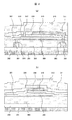
- FIG. 2A is a cross-sectional view taken along the line A-A ′ in FIG. 1
- FIG. 2B is a cross-sectional view taken along the line B-B ′ in FIG. 1.
- A) shows the manufacturing process of the ultrasonic transducer, and is a cross-sectional view cut along the line AA ′ in FIG. 1, and
- FIG. 6 is a cross-sectional view taken along line ⁇ B ′.
- (A) is sectional drawing which showed the manufacturing process of the ultrasonic transducer following FIG.
- FIG. 3 (a), (b) is sectional drawing which showed the manufacturing process of the ultrasonic transducer following FIG.3 (b).
- A) is sectional drawing which showed the manufacturing process of the ultrasonic transducer following FIG. 4 (a)
- (b) is sectional drawing which showed the manufacturing process of the ultrasonic transducer following FIG.4 (b).
- A) is sectional drawing which showed the manufacturing process of the ultrasonic transducer following FIG. 5 (a)
- (b) is sectional drawing which showed the manufacturing process of the ultrasonic transducer following FIG.5 (b).
- A) is sectional drawing which showed the manufacturing process of the ultrasonic transducer following FIG.
- FIG. 6 (a), (b) is sectional drawing which showed the manufacturing process of the ultrasonic transducer following FIG.6 (b).
- A) is sectional drawing which showed the manufacturing process of the ultrasonic transducer following FIG. 7 (a)
- (b) is sectional drawing which showed the manufacturing process of the ultrasonic transducer following FIG.7 (b).
- A) is sectional drawing which showed the manufacturing process of the ultrasonic transducer following FIG. 8 (a)
- FIG.8 (b) is sectional drawing which showed the manufacturing process of the ultrasonic transducer following FIG.8 (b).
- A) is sectional drawing which showed the manufacturing process of the ultrasonic transducer following FIG.
- FIG. 9 (a), (b) is sectional drawing which showed the manufacturing process of the ultrasonic transducer following FIG.9 (b).
- A) is sectional drawing which showed the manufacturing process of the ultrasonic transducer following FIG. 10 (a)
- (b) is sectional drawing which showed the manufacturing process of the ultrasonic transducer following FIG.10 (b).
- A) is sectional drawing which showed the manufacturing process of the ultrasonic transducer following FIG. 11 (a)
- (b) is sectional drawing which showed the manufacturing process of the ultrasonic transducer following FIG.11 (b).
- A) is sectional drawing which showed the manufacturing process of the ultrasonic transducer following FIG.
- Example 1 it is sectional drawing which showed the manufacturing method in the case of forming a lower electrode, after forming the electrical connection part to a lower electrode.
- 2A is a cross-sectional view taken along the line A-A ′ in FIG. 1
- FIG. 2B is a cross-sectional view taken along the line B-B ′ in FIG. 1.
- FIG. 15A is a cross-sectional view showing a manufacturing process of the ultrasonic transducer following FIG. 15A
- FIG. 15B is a cross-sectional view showing a manufacturing process of the ultrasonic transducer following FIG. (A) is sectional drawing which showed the manufacturing process of the ultrasonic transducer following FIG. 16 (a)
- (b) is sectional drawing which showed the manufacturing process of the ultrasonic transducer following FIG.16 (b).
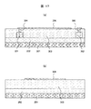
- FIG. 18A is a cross-sectional view of an ultrasonic transducer manufactured by a manufacturing method in the case where a lower electrode is formed after the electrical connection portion to the lower electrode shown in FIGS. 15 to 17 is formed
- FIG. 2 is a cross-sectional view taken along line AA ′ of FIG.
- FIG. 5B is a cross-sectional view taken along line BB ′ of FIG. It is the top view which showed the ultrasonic transducer of the arrangement
- the deformation of the cavity is suppressed, the uniformity of the insulating film, and the deterioration of the flatness of the membrane surface shape are reduced.
- the purpose of suppression is realized by arranging the electrical connection portion to the lower electrode so as not to overlap the cavity portion when viewed from above.
- FIG. 1 is a top view of one CMUT cell.
- 306 is a lower electrode
- 308 is a cavity
- 310 is an upper electrode
- 312 is an etching hole for forming the cavity 308. That is, the etching hole 312 is connected to the cavity 308.
- Reference numeral 304 denotes a connection part that electrically connects to the lower electrode 306 from the lower layer
- reference numeral 305 denotes a connection part that electrically connects to the upper electrode from the lower layer.
- An insulating film is formed between the upper electrode 310 and the lower electrode 306 so as to cover the cavity 308 and the lower electrode 306, but is not shown to show the cavity 308 and the lower electrode 306.
- FIG. 2A shows the A-A ′ cross section of FIG. 1
- FIG. 2B shows the B-B ′ cross section of FIG.
- wirings 301 and 302 are formed on the upper surface of the insulating film 202 on the semiconductor substrate 201, and an insulating film 303 is formed so as to cover the wiring.
- connection portions 304 and 305 electrically connected to the lower electrode and the upper electrode of the CMUT are formed on the wirings 301 and 302.
- the connection portions 304 and 305 are connected to the lower electrode 306 and the upper electrode 310, respectively. .
- a cavity 308 is formed above the lower electrode 306 with an insulating film 307 interposed therebetween.
- An insulating film 309 is formed so as to surround the cavity 308, and an upper electrode 310 is formed on the insulating film 309.
- An insulating film 311 and an insulating film 313 are formed on the upper layer of the upper electrode 310. Further, the insulating film 309 and the insulating film 311 are formed with etching holes 312 penetrating these films.
- the etching hole 312 is formed to form the cavity 308, and is filled with an insulating film 313 after the cavity 308 is formed.
- the membrane that vibrates when the CMUT is driven is composed of insulating films 309, 311, 313 and an upper electrode 310.
- the feature of the first embodiment is that, as shown in FIGS. 1 and 2A and 2B, the electrical connection 304 to the lower electrode 306 is arranged so as not to overlap the cavity 308 when viewed from above. It is in. With this arrangement, even when electrical connection is performed from the lower surface of each electrode, the cavity 308 can be formed without being affected by the shape of the electrical connection portion 304, and similarly, the upper layer membrane Will not be affected. Therefore, deformation of the cavity and non-uniformity of the insulating film thickness surrounding the cavity can be suppressed, and further, deterioration of the flatness of the surface shape of the membrane can be suppressed.
- the electrical connection portion 304 to the lower electrode 306 is arranged so as not to overlap the cavity portion 308 when viewed from the upper surface, even when electrical connection is performed from the lower surface of the lower electrode, the electrical connection is performed.
- the cavity 308 and the membrane can be formed without being affected by the shape of the portion 304, and variations in ultrasonic characteristics of each cell can be suppressed.
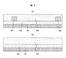
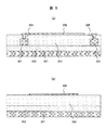
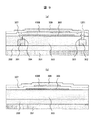
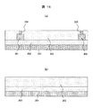
- FIGS. 3 to 14 shows the AA ′ cross-sectional direction in FIG. 1, and (b) in FIGS. 3 to 14 shows the BB ′ cross-sectional direction in FIG. Show.
- an insulating film 202 made of a 400 nm silicon oxide film is formed on a semiconductor substrate 201 by plasma CVD (Chemical Vapor Deposition).
- Wirings 301 and 302 in which titanium nitride 50 nm, aluminum alloy 600 nm and titanium nitride 50 nm are stacked are formed on the insulating film 202, and then an insulating film 303 made of a 500 nm silicon oxide film is formed by plasma CVD, and wirings 301 and 302 are formed. Form to cover.
- the insulating film 303 is planarized by a CMP (Chemical-Mechanical-Polishing) method.
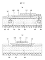
- openings 704 and 705 reaching the wirings 301 and 302 are formed in the insulating film 303 by a lithography technique and a dry etching technique (FIGS. 4A and 4B).
- a conductive film having a thickness of 100 nm to be the lower electrode of the CMUT is formed by a sputtering method.
- the openings 704 and 705 are also embedded.
- the lower electrode 306, the electrical connection portion 304 to the lower electrode, and the electrical connection portion 305 to the upper electrode are formed by lithography technology and dry etching technology (FIGS. 5A and 5B).
- the conductive film to be the lower electrode 306 is conductive such as tungsten (W), titanium (Ti), aluminum (Al), copper (Cu), and their alloys, nitrides, silicon compounds and the like used in normal semiconductor processes. If there is. Since it is connected to the lower electrode by the wiring 301 in the immediate vicinity of the CMUT cell, the decrease in resistance can be suppressed to a small value, and the conductive film may be about 100 nm thick.
- an insulating film 307 made of a silicon oxide film is deposited on the lower electrode 306 by plasma CVD (FIGS. 6A and 6B).
- an amorphous silicon film is deposited to a thickness of 100 nm on the upper surface of the insulating film 307 made of a silicon oxide film by a plasma CVD method, and then the sacrificial layer 1008 is formed by processing the amorphous silicon film by a lithography technique and a dry etching technique. (FIGS. 7A and 7B).
- the sacrificial layer pattern is arranged so as not to overlap with the connection portion 304 with the lower electrode as viewed from above. This sacrificial layer becomes a cavity in a subsequent process.
- an insulating film 309 made of a silicon oxide film is deposited by a plasma CVD method so as to cover the sacrificial layer 1008 and the insulating film 307 made of a silicon oxide film. (FIGS. 8A and 8B).
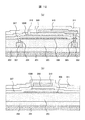
- an opening 1201 reaching the electrical connection portion 305 for the upper electrode is formed in the insulating films 307 and 309 by lithography and dry etching (FIGS. 9A and 9B).
- the upper electrode 310 of the CMUT a laminated film of a titanium nitride film, an aluminum alloy film, and a titanium nitride film is deposited by sputtering to a thickness of 50 nm, 300 nm, and 50 nm, respectively. Then, the upper electrode 310 is formed by a lithography technique and a dry etching technique. At this time, the opening 1201 formed in the insulating films 307 and 309 is also buried at the same time, and the upper electrode 310 and the wiring 302 are connected via the electrical connection portion 305 (FIGS. 10A and 10B).
- an insulating film 311 made of a silicon nitride film is deposited by a plasma CVD method so as to cover the silicon oxide film 309 and the upper electrode 310 (FIGS. 11A and 11B).
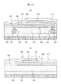
- an etching hole 312 reaching the sacrificial layer 1008 is formed in the insulating film 311 made of a silicon nitride film and the insulating film 309 made of a silicon oxide film using a lithography technique and a dry etching technique (FIGS. 12A and 12B). b)).
- the sacrificial layer 1008 is etched with xenon fluoride gas (XeF 2) through the opening 312 to form the cavity 308 (FIGS. 13A and 13B).
- XeF 2 xenon fluoride gas
- an insulating film 313 made of a silicon nitride film is deposited by a plasma CVD method to a thickness of about 800 nm (FIGS. 14A and 14B).
- the CMUT in the first embodiment can be formed.
- a conductive film as a material for the lower electrode is simultaneously buried in the opening 704 formed on the lower layer wiring to form the electrical connection portion 304 to the lower electrode. It is also possible to form the lower electrode after forming the electrical connection to the electrode.
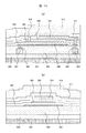
- the manufacturing method in that case is shown in FIGS. After FIGS. 4A and 4B, a conductive film 1801 is deposited by a sputtering method. At this time, the film thickness that can be filled in the openings 704 and 705 shown in FIG. 4A is deposited (FIGS. 15A and 15B).
- the conductive film 1801 deposited on the insulating film 303 is polished by CMP until the upper surface of the insulating film 303 is exposed.
- the upper surfaces of the connection portions 304 and 305 are insulated by the recess in the CMP process.
- the structure is slightly recessed from the upper surface of the film 303 (FIGS. 16A and 16B).
- the conductive film to be the lower electrode is made 100 nm by a sputtering method, and the lower electrode 306 is formed by a lithography technique and a dry etching technique (FIGS. 17A and 17B). The subsequent processes are the same as those in FIG.
- FIG. 18 shows a cross-sectional view of the CMUT manufactured by this method.
- the conductive film 1801 is first embedded in the openings 704 and 705 formed in the insulating film 303 shown in FIG. 4, and then the lower electrode is formed.
- the opening diameters of the openings 704 and 705 are large, there is a possibility that the openings 704 and 705 may not be filled with a 100 nm conductive film serving as a lower electrode in the steps shown in FIGS. In that case, the conductive film deposited in the openings 704 and 705 is disconnected at the bottom surface of the opening, which causes poor electrical connection with the lower electrode and the upper electrode.
- the lower electrode when a conductive film having a film thickness that can fill the openings 704 and 705 is deposited, the lower electrode is also thickened, resulting in a large step due to the lower electrode, and withstand voltage at a position where the upper electrode gets over the step of the lower electrode. Decreases.
- the conductive film in the lower electrode formation step can be as thin as about 100 nm.
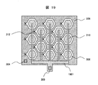
- a CMUT cell in which one cavity is overlapped with one lower electrode as shown in FIG. 1 is the same as in the case where a plurality of cavities are overlapped with one lower electrode as shown in FIG. is there. That is, in FIG. 19, 13 cavities 308 overlap with the lower electrode 306.
- the individual upper electrodes 310 are arranged so as to overlap the 13 cavities 308, and are bundled by wiring 1901 and connected to the electrical connection portion 305. Also in this embodiment, as in FIG.
- the electrical connection 304 to the lower electrode 306 is arranged so as not to overlap the cavity 308 when viewed from the upper surface, and even when the electrical connection is performed from the lower surface of each electrode,
- the cavity portion 308 can be formed without being affected by the shape of the electrical connection portion 304, and similarly, the upper layer membrane is not affected. Therefore, deformation of the cavity and non-uniformity of the insulating film thickness surrounding the cavity can be suppressed, and further, deterioration of the flatness of the surface shape of the membrane can be suppressed.
- the CMUT cavity 308 has a hexagonal shape when viewed from above, but the shape is not limited to this and may be any shape.
- the material constituting the CMUT shown as the first embodiment is one of the combinations, and other conductive materials may be used as the material of the upper electrode and the lower electrode.
- the material of the sacrificial layer may be any material that can ensure etching selectivity with the insulating film surrounding the sacrificial layer. Therefore, in addition to the amorphous silicon film, an SOG film (Spin-on-Glass) or a metal film such as aluminum, tungsten, molybdenum, or chromium may be used. In the case of the SOG film as well, the use of hydrofluoric acid can ensure the etching selectivity with the insulating film surrounding the sacrificial layer.
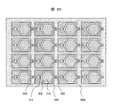
- FIG. 20 is a top view of the ultrasonic transducer in which the CMUT cells shown in FIG. 1 are arranged in an array.
- 306 is a lower electrode
- 308 is a cavity
- 310 is an upper electrode
- 312 is an etching hole for forming the cavity 308. That is, the etching hole 312 is connected to the cavity 308.
- Reference numeral 304 denotes a connection part that electrically connects to the lower electrode 306 from the lower layer
- reference numeral 305 denotes a connection part that electrically connects to the upper electrode from the lower layer.
- Reference numeral 2001 denotes a semiconductor substrate on which an array is arranged. The cross-sectional structure of the individual CMUT cells constituting the array is the same as that shown in FIG.
- FIG. 21 is a top view of the ultrasonic transducer in which the CMUT cells shown in FIG. 19 are arranged in an array.
- 306 is a lower electrode
- 308 is a cavity
- 310 is an upper electrode
- 312 is an etching hole for forming the cavity 308. That is, the etching hole 312 is connected to the cavity 308.
- Reference numeral 304 denotes a connection portion that performs electrical connection from the lower layer to the lower electrode 306.
- Reference numeral 1901 denotes a wiring connecting between the upper electrodes 310 corresponding to the hollow portions constituting one CMUT cell
- reference numeral 305 denotes a connection portion for electrically connecting to the wiring 1901 from the lower layer.
- Reference numeral 2001 denotes a semiconductor substrate arranged in an array. The cross-sectional structure of the individual CMUT cells constituting the array is the same as that shown in FIG.
- the CMUT cells are arranged in an array.
- the feature is that the electrical connection 304 to the lower electrode 306 of each CMUT cell can be seen from the top surface as a cavity.
- the arrangement is that it does not overlap the portion 308.
- the cavity 308 can be formed without being affected by the shape of the electrical connection portion 304, and similarly, the upper layer membrane Will not be affected. Therefore, deformation of the cavity and non-uniformity of the insulating film thickness surrounding the cavity can be suppressed, and further, deterioration of the flatness of the surface shape of the membrane can be suppressed.
- the ultrasonic transducer of the present invention can be widely used as a transducer for an ultrasonic diagnostic apparatus, an ultrasonic flaw detector, and the like.
Landscapes
- Engineering & Computer Science (AREA)
- Manufacturing & Machinery (AREA)
- Microelectronics & Electronic Packaging (AREA)
- Mechanical Engineering (AREA)
- Physics & Mathematics (AREA)
- Geometry (AREA)
- Transducers For Ultrasonic Waves (AREA)
- Ultra Sonic Daignosis Equipment (AREA)
- Pressure Sensors (AREA)
- Micromachines (AREA)
Abstract
Description
102 空洞部
103 絶縁膜
104 上部電極
105 メンブレン
106 下部電極への電気接続部
107 CMUTセルの下層に配置された配線
108 絶縁膜
201 半導体基板
202 絶縁膜
301 CMUTセルの下層に配置された配線
302 CMUTセルの下層に配置された配線
303 絶縁膜
304 下部電極への電気接続部
305 上部電極への電気接続部
306 下部電極
307 絶縁膜
308 空洞部
309 絶縁膜
310 上部電極
311 絶縁膜
312 エッチング孔
313 絶縁膜
704 開口部
705 開口部
1008 犠牲層
1201 開口部
1801 導電膜
1901 配線
2001 半導体基板。
Claims (8)
- (a)下部電極と、
(b)前記下部電極の下面から前記下部電極へ接続する電気接続部と、
(c)前記下部電極を覆うように形成された第1絶縁膜と、
(d)前記第1絶縁膜上に、上面から見て、前記下部電極と重なるように形成された空洞部と、
(e)前記空洞部を覆うように形成された第2絶縁膜と、
(f)前記第2絶縁膜上に、上面から見て、前記空洞部と重なるように形成された上部電極とを備えた超音波トランスデューサにおいて、
(g)前記電気接続部が、上面から見て、前記空洞部と重ならない位置に配置されていることを特徴とする超音波トランスデューサ。 - (a)複数の下部電極と、
(b)前記複数の下部電極のそれぞれの下面から前記複数の下部電極へ接続する複数の電気接続部と、
(c)前記複数の下部電極を覆うように形成された第1絶縁膜と、
(d)前記第1絶縁膜上に、上面から見て、前記複数の下部電極とそれぞれ重なるように形成された複数の空洞部と、
(e)前記複数の空洞部を覆うように形成された第2絶縁膜と、
(f)前記第2絶縁膜上に、上面から見て、前記複数の空洞部とそれぞれ重なるように形成された複数の上部電極とを備えた超音波トランスデューサにおいて、
(g)前記複数の電気接続部が、上面から見て、前記複数の空洞部とそれぞれ重ならない位置に配置されていることを特徴とする超音波トランスデューサ。 - 請求項1または請求項2記載の超音波トランスデューサにおいて、さらに、
(h)半導体基板と、
(i)前記半導体基板上に形成された配線と、
(j)前記配線を覆うように形成された第3絶縁膜とを備え、
(k)前記第3絶縁膜の開口部を通して、前記電気接続部の他端が前記配線と接続されている超音波トランスデューサ。 - 請求項3記載の超音波トランスデューサにおいて、さらに、
(l)第2の電気接続部を備え、
(m)前記第3絶縁膜の開口部を通して、前記第2の電気接続部の一端が前記上部電極と接続され、他端が半導体基板上に形成された前記配線と接続されている超音波トランスデューサ。 - 請求項1乃至請求項4のいずれか一つに記載の超音波トランスデューサを用いた超音波探触子。
- (a)配線を形成する工程と、
(b)前記配線を覆う第1絶縁膜を形成する工程と、
(c)前記第1絶縁膜を平坦化する工程と、
(d)前記第1絶縁膜に前記配線に達する第1開口部を形成する工程と、
(e)前記第1開口部に導電膜を埋め込み、電気接続部を形成する工程と、
(f)前記電気接続部上に下部電極を形成する工程と、
(g)前記下部電極を覆うように第2絶縁膜を形成する工程と、
(h)前記第1絶縁膜上に、上面から見て、前記下部電極と重なるように、かつ、前記電気接続部と重ならない位置に犠牲層を形成する工程と、
(i)前記犠牲層を覆うように第3絶縁膜を形成する工程と、
(j)前記第3絶縁膜上に、上面からみて、前記犠牲層と重なるように上部電極を形成する工程と、
(k)前記上部電極および前記第3絶縁膜を覆う第4絶縁膜を形成する工程と、
(l)前記第3絶縁膜および前記第4絶縁膜を貫通して前記犠牲層に達する第2開口部を形成する工程と、
(m)前記第2開口部を利用して前記犠牲層を除去することにより空洞部を形成する工程と、
(n)前記第2絶縁膜と前記犠牲層に達する開口部を覆うように第5絶縁膜を形成し、前記空洞部を封止する工程とを備える超音波トランスデューサの製造方法。 - 請求項6記載の超音波トランスデューサの製造方法において、
前記第1開口部に導電膜を埋め込み、電気接続部を形成する工程と、前記電気接続部上に下部電極を形成する工程とを、一つの工程で行うことを特徴とする超音波トランスデューサの製造方法。 - 請求項6または請求項7記載の超音波トランスデューサの製造方法において、
前記配線を形成する工程が、半導体基板上に前記配線を形成するものであることを特徴とする超音波トランスデューサの製造方法。
Priority Applications (3)
| Application Number | Priority Date | Filing Date | Title |
|---|---|---|---|
| JP2011502625A JP5851238B6 (ja) | 2009-03-05 | 2010-02-23 | 超音波トランスデューサ、その製造方法、および、それを用いた超音波探触子 |
| US13/201,114 US20110316383A1 (en) | 2009-03-05 | 2010-02-23 | Ultrasonic transducer, method of producing same, and ultrasonic probe using same |
| US14/799,632 US9873137B2 (en) | 2009-03-05 | 2015-07-15 | Ultrasonic transducer, method of producing same, and ultrasonic probe using same |
Applications Claiming Priority (2)
| Application Number | Priority Date | Filing Date | Title |
|---|---|---|---|
| JP2009052125 | 2009-03-05 | ||
| JP2009-052125 | 2009-03-05 |
Related Child Applications (2)
| Application Number | Title | Priority Date | Filing Date |
|---|---|---|---|
| US13/201,114 A-371-Of-International US20110316383A1 (en) | 2009-03-05 | 2010-02-23 | Ultrasonic transducer, method of producing same, and ultrasonic probe using same |
| US14/799,632 Division US9873137B2 (en) | 2009-03-05 | 2015-07-15 | Ultrasonic transducer, method of producing same, and ultrasonic probe using same |
Publications (1)
| Publication Number | Publication Date |
|---|---|
| WO2010100861A1 true WO2010100861A1 (ja) | 2010-09-10 |
Family
ID=42709431
Family Applications (1)
| Application Number | Title | Priority Date | Filing Date |
|---|---|---|---|
| PCT/JP2010/001200 Ceased WO2010100861A1 (ja) | 2009-03-05 | 2010-02-23 | 超音波トランスデューサ、その製造方法、および、それを用いた超音波探触子 |
Country Status (3)
| Country | Link |
|---|---|
| US (2) | US20110316383A1 (ja) |
| JP (1) | JP5851238B6 (ja) |
| WO (1) | WO2010100861A1 (ja) |
Cited By (8)
| Publication number | Priority date | Publication date | Assignee | Title |
|---|---|---|---|---|
| WO2012075106A1 (en) * | 2010-12-03 | 2012-06-07 | Research Triangle Institute | Method for forming an ultrasonic transducer, and associated apparatus |
| JP2012222516A (ja) * | 2011-04-06 | 2012-11-12 | Canon Inc | 電気機械変換装置及びその作製方法 |
| US9510069B2 (en) | 2011-04-06 | 2016-11-29 | Canon Kabushiki Kaisha | Electromechanical transducer and method of producing the same |
| WO2016194591A1 (ja) * | 2015-05-29 | 2016-12-08 | 株式会社日立製作所 | 超音波トランスデューサおよび超音波検査装置 |
| US20200101492A1 (en) * | 2018-09-28 | 2020-04-02 | Canon Kabushiki Kaisha | Capacitive transducer, manufacturing method thereof, and image forming apparatus |
| JP2021185700A (ja) * | 2018-04-11 | 2021-12-09 | エコー イメージング,インク. | 圧電トランシーバーを有する画像処理装置 |
| US11986350B2 (en) | 2016-12-04 | 2024-05-21 | Exo Imaging, Inc. | Imaging devices having piezoelectric transducers |
| US12053323B2 (en) * | 2018-05-03 | 2024-08-06 | Bfly Operations Inc | Pressure port for ultrasonic transducer on CMOS sensor |
Families Citing this family (6)
| Publication number | Priority date | Publication date | Assignee | Title |
|---|---|---|---|---|
| JP5851238B6 (ja) | 2009-03-05 | 2023-12-15 | 株式会社日立メディコ | 超音波トランスデューサ、その製造方法、および、それを用いた超音波探触子 |
| KR101919013B1 (ko) * | 2012-09-13 | 2019-02-08 | 삼성전자주식회사 | 미세가공 초음파 변환기 어레이 |
| JP6416232B2 (ja) * | 2013-09-24 | 2018-10-31 | コーニンクレッカ フィリップス エヌ ヴェKoninklijke Philips N.V. | Cmutデバイス製造方法、cmutデバイス、及び装置 |
| JP6555869B2 (ja) * | 2014-10-17 | 2019-08-07 | キヤノン株式会社 | 静電容量型トランスデューサ |
| WO2017018967A1 (en) * | 2015-07-30 | 2017-02-02 | Intel IP Corporation | Apparatus, system and method of providing wlan measurement information from a cellular node to a location server |
| JP2017112187A (ja) * | 2015-12-15 | 2017-06-22 | キヤノン株式会社 | 貫通配線を有する基板に素子を設けたデバイス及びその製造方法 |
Citations (3)
| Publication number | Priority date | Publication date | Assignee | Title |
|---|---|---|---|---|
| JP2006211185A (ja) * | 2005-01-27 | 2006-08-10 | Hitachi Ltd | 超音波トランスデューサおよびその製造方法 |
| JP2007097760A (ja) * | 2005-10-03 | 2007-04-19 | Olympus Medical Systems Corp | 静電容量型超音波振動子装置 |
| JP2007229327A (ja) * | 2006-03-03 | 2007-09-13 | Olympus Medical Systems Corp | 超音波振動子及びそれを搭載した体腔内超音波診断装置 |
Family Cites Families (14)
| Publication number | Priority date | Publication date | Assignee | Title |
|---|---|---|---|---|
| DE19643893A1 (de) | 1996-10-30 | 1998-05-07 | Siemens Ag | Ultraschallwandler in Oberflächen-Mikromechanik |
| US6271620B1 (en) | 1999-05-20 | 2001-08-07 | Sen Corporation | Acoustic transducer and method of making the same |
| US6246158B1 (en) | 1999-06-24 | 2001-06-12 | Sensant Corporation | Microfabricated transducers formed over other circuit components on an integrated circuit chip and methods for making the same |
| US6430109B1 (en) | 1999-09-30 | 2002-08-06 | The Board Of Trustees Of The Leland Stanford Junior University | Array of capacitive micromachined ultrasonic transducer elements with through wafer via connections |
| JP4790315B2 (ja) * | 2005-05-31 | 2011-10-12 | オリンパスメディカルシステムズ株式会社 | 静電容量型超音波振動子 |
| JP4724501B2 (ja) * | 2005-09-06 | 2011-07-13 | 株式会社日立製作所 | 超音波トランスデューサおよびその製造方法 |
| JP4839099B2 (ja) * | 2006-03-03 | 2011-12-14 | オリンパスメディカルシステムズ株式会社 | マイクロマシンプロセスにより製造された超音波振動子、超音波振動子装置、その体腔内超音波診断装置、及びその制御方法 |
| JP4979283B2 (ja) * | 2006-06-29 | 2012-07-18 | 株式会社日立製作所 | 半導体装置の製造方法および半導体装置 |
| JP5016884B2 (ja) * | 2006-09-29 | 2012-09-05 | 株式会社日立製作所 | 半導体装置およびその製造方法 |
| JP2008099036A (ja) * | 2006-10-12 | 2008-04-24 | Olympus Medical Systems Corp | 超音波トランスデューサ、超音波探触子及び超音波診断装置 |
| CN101636112B (zh) * | 2007-03-20 | 2011-10-26 | 株式会社日立医药 | 超声波探头及其制造方法及超声波诊断装置 |
| JP4961260B2 (ja) | 2007-05-16 | 2012-06-27 | 株式会社日立製作所 | 半導体装置 |
| US8047995B2 (en) * | 2007-08-28 | 2011-11-01 | Olympus Medical Systems Corp. | Ultrasonic transducer, method of manufacturing ultrasonic transducer, ultrasonic diagnostic apparatus, and ultrasonic microscope |
| JP5851238B6 (ja) | 2009-03-05 | 2023-12-15 | 株式会社日立メディコ | 超音波トランスデューサ、その製造方法、および、それを用いた超音波探触子 |
-
2010
- 2010-02-23 JP JP2011502625A patent/JP5851238B6/ja active Active
- 2010-02-23 WO PCT/JP2010/001200 patent/WO2010100861A1/ja not_active Ceased
- 2010-02-23 US US13/201,114 patent/US20110316383A1/en not_active Abandoned
-
2015
- 2015-07-15 US US14/799,632 patent/US9873137B2/en active Active
Patent Citations (3)
| Publication number | Priority date | Publication date | Assignee | Title |
|---|---|---|---|---|
| JP2006211185A (ja) * | 2005-01-27 | 2006-08-10 | Hitachi Ltd | 超音波トランスデューサおよびその製造方法 |
| JP2007097760A (ja) * | 2005-10-03 | 2007-04-19 | Olympus Medical Systems Corp | 静電容量型超音波振動子装置 |
| JP2007229327A (ja) * | 2006-03-03 | 2007-09-13 | Olympus Medical Systems Corp | 超音波振動子及びそれを搭載した体腔内超音波診断装置 |
Cited By (13)
| Publication number | Priority date | Publication date | Assignee | Title |
|---|---|---|---|---|
| WO2012075106A1 (en) * | 2010-12-03 | 2012-06-07 | Research Triangle Institute | Method for forming an ultrasonic transducer, and associated apparatus |
| CN103347620A (zh) * | 2010-12-03 | 2013-10-09 | 三角形研究学会 | 用于形成超声换能器的方法及相关装置 |
| US8692441B2 (en) | 2010-12-03 | 2014-04-08 | Research Triangle Institute | Method for forming an ultrasonic transducer, and associated apparatus |
| JP2012222516A (ja) * | 2011-04-06 | 2012-11-12 | Canon Inc | 電気機械変換装置及びその作製方法 |
| US9510069B2 (en) | 2011-04-06 | 2016-11-29 | Canon Kabushiki Kaisha | Electromechanical transducer and method of producing the same |
| JPWO2016194591A1 (ja) * | 2015-05-29 | 2018-03-15 | 株式会社日立製作所 | 超音波トランスデューサおよび超音波検査装置 |
| WO2016194591A1 (ja) * | 2015-05-29 | 2016-12-08 | 株式会社日立製作所 | 超音波トランスデューサおよび超音波検査装置 |
| US11986350B2 (en) | 2016-12-04 | 2024-05-21 | Exo Imaging, Inc. | Imaging devices having piezoelectric transducers |
| JP2021185700A (ja) * | 2018-04-11 | 2021-12-09 | エコー イメージング,インク. | 圧電トランシーバーを有する画像処理装置 |
| US11774280B2 (en) | 2018-04-11 | 2023-10-03 | Exo Imaging, Inc. | Imaging devices having piezoelectric transceivers |
| JP7417286B2 (ja) | 2018-04-11 | 2024-01-18 | エコー イメージング,インク. | 圧電トランシーバーを有する画像処理装置 |
| US12053323B2 (en) * | 2018-05-03 | 2024-08-06 | Bfly Operations Inc | Pressure port for ultrasonic transducer on CMOS sensor |
| US20200101492A1 (en) * | 2018-09-28 | 2020-04-02 | Canon Kabushiki Kaisha | Capacitive transducer, manufacturing method thereof, and image forming apparatus |
Also Published As
| Publication number | Publication date |
|---|---|
| US9873137B2 (en) | 2018-01-23 |
| JP5851238B6 (ja) | 2023-12-15 |
| US20110316383A1 (en) | 2011-12-29 |
| JPWO2010100861A1 (ja) | 2012-09-06 |
| US20160008849A1 (en) | 2016-01-14 |
| JP5851238B2 (ja) | 2016-02-03 |
Similar Documents
| Publication | Publication Date | Title |
|---|---|---|
| JP5851238B2 (ja) | 超音波トランスデューサ、その製造方法、および、それを用いた超音波探触子 | |
| EP1992421B1 (en) | Semiconductor device | |
| US7512038B2 (en) | Ultrasonic transducer and manufacturing method | |
| EP1908529B1 (en) | Manufacturing method of an ultrasonic transducer | |
| JP2010004199A (ja) | 超音波トランスデューサおよびその製造方法 | |
| JP2007527285A (ja) | 多要素電極cmut素子及び製作方法 | |
| JP4471856B2 (ja) | 超音波トランスデューサおよびその製造方法 | |
| US20130069480A1 (en) | Electromechanical transducer and method of manufacturing the electromechanical transducer | |
| CN105731362A (zh) | 器件的制作方法 | |
| JP6267787B2 (ja) | 超音波トランスデューサ及びその製造方法、並びに超音波検査装置 | |
| JP2015128271A (ja) | 静電容量型トランスデューサ及びその製造方法 | |
| JPWO2016194208A1 (ja) | 超音波トランスデューサ素子、その製造方法及び超音波撮像装置 | |
| JP6306705B2 (ja) | 超音波探触子、その性能評価方法及び超音波診断装置 | |
| JP6470406B2 (ja) | 超音波トランスデューサおよび超音波検査装置 | |
| JP7141934B2 (ja) | 超音波トランスデューサ、その製造方法および超音波撮像装置 | |
| JP6390428B2 (ja) | 超音波振動子セル、超音波プローブ、及び超音波振動子セルの制御方法 | |
| US12486159B2 (en) | Micro-machined ultrasound transducers with insulation layer and methods of manufacture | |
| JP5535277B2 (ja) | 超音波トランスデューサの製造方法 | |
| JP5085717B2 (ja) | 超音波トランスデューサの製造方法 |
Legal Events
| Date | Code | Title | Description |
|---|---|---|---|
| 121 | Ep: the epo has been informed by wipo that ep was designated in this application |
Ref document number: 10748463 Country of ref document: EP Kind code of ref document: A1 |
|
| ENP | Entry into the national phase |
Ref document number: 2011502625 Country of ref document: JP Kind code of ref document: A |
|
| WWE | Wipo information: entry into national phase |
Ref document number: 13201114 Country of ref document: US |
|
| NENP | Non-entry into the national phase |
Ref country code: DE |
|
| 122 | Ep: pct application non-entry in european phase |
Ref document number: 10748463 Country of ref document: EP Kind code of ref document: A1 |