WO2010097861A1 - Dispositif à faisceaux de particules chargées - Google Patents
Dispositif à faisceaux de particules chargées Download PDFInfo
- Publication number
- WO2010097861A1 WO2010097861A1 PCT/JP2009/005581 JP2009005581W WO2010097861A1 WO 2010097861 A1 WO2010097861 A1 WO 2010097861A1 JP 2009005581 W JP2009005581 W JP 2009005581W WO 2010097861 A1 WO2010097861 A1 WO 2010097861A1
- Authority
- WO
- WIPO (PCT)
- Prior art keywords
- sample
- detector
- optical system
- charged particle
- electron beam
- Prior art date
Links
Images


Classifications
-
- H—ELECTRICITY
- H01—ELECTRIC ELEMENTS
- H01J—ELECTRIC DISCHARGE TUBES OR DISCHARGE LAMPS
- H01J37/00—Discharge tubes with provision for introducing objects or material to be exposed to the discharge, e.g. for the purpose of examination or processing thereof
- H01J37/02—Details
- H01J37/244—Detectors; Associated components or circuits therefor
-
- H—ELECTRICITY
- H01—ELECTRIC ELEMENTS
- H01J—ELECTRIC DISCHARGE TUBES OR DISCHARGE LAMPS
- H01J37/00—Discharge tubes with provision for introducing objects or material to be exposed to the discharge, e.g. for the purpose of examination or processing thereof
- H01J37/26—Electron or ion microscopes; Electron or ion diffraction tubes
- H01J37/261—Details
- H01J37/265—Controlling the tube; circuit arrangements adapted to a particular application not otherwise provided, e.g. bright-field-dark-field illumination
-
- H—ELECTRICITY
- H01—ELECTRIC ELEMENTS
- H01J—ELECTRIC DISCHARGE TUBES OR DISCHARGE LAMPS
- H01J37/00—Discharge tubes with provision for introducing objects or material to be exposed to the discharge, e.g. for the purpose of examination or processing thereof
- H01J37/26—Electron or ion microscopes; Electron or ion diffraction tubes
- H01J37/28—Electron or ion microscopes; Electron or ion diffraction tubes with scanning beams
-
- H—ELECTRICITY
- H01—ELECTRIC ELEMENTS
- H01J—ELECTRIC DISCHARGE TUBES OR DISCHARGE LAMPS
- H01J2237/00—Discharge tubes exposing object to beam, e.g. for analysis treatment, etching, imaging
- H01J2237/02—Details
- H01J2237/024—Moving components not otherwise provided for
-
- H—ELECTRICITY
- H01—ELECTRIC ELEMENTS
- H01J—ELECTRIC DISCHARGE TUBES OR DISCHARGE LAMPS
- H01J2237/00—Discharge tubes exposing object to beam, e.g. for analysis treatment, etching, imaging
- H01J2237/244—Detection characterized by the detecting means
- H01J2237/24455—Transmitted particle detectors
-
- H—ELECTRICITY
- H01—ELECTRIC ELEMENTS
- H01J—ELECTRIC DISCHARGE TUBES OR DISCHARGE LAMPS
- H01J2237/00—Discharge tubes exposing object to beam, e.g. for analysis treatment, etching, imaging
- H01J2237/244—Detection characterized by the detecting means
- H01J2237/24475—Scattered electron detectors
Definitions
- the present invention relates to a charged particle beam apparatus that can irradiate an ion beam, an electron beam, or the like.
- a focused ion beam (Focused Ion Beam: hereinafter referred to as FIB) apparatus is used to cut out the predetermined site from the sample, and a thin film sample for STEM or TEM observation is prepared. Observation by TEM is increasing.
- FIB focused ion beam
- FIB-SEM dual beam
- Patent Document 1 discloses a focused ion beam optical system, an electron beam optical system, a sample stage on which a sample is placed, and a micro sample extracted from a sample by focused ion beam processing.
- a micro sample processing and observation apparatus having a second sample stage to be held, it is disclosed that the angle of the second sample stage is adjusted so that the micro sample has an appropriate angle with respect to the electron beam.
- the inventor of the present application has earnestly studied the high-precision sample observation in the FIB-SEM apparatus, particularly the relationship with the incident angle of the charged particle beam to the sample surface, and as a result, the following knowledge has been obtained.
- the optimum position of the detection signal with respect to the beam changes.
- the detector position is fixed, the required signal intensity may not be ensured.
- an FIB-SEM apparatus having a point (cross point) at which both beams of an ion beam electron optical system and an electron beam electron optical system cross each other performs main processing and observation of a sample at the cross point. They are arranged at an angle so as not to physically interfere with each other around the sample position (for example, 60 °). For this reason, the optimum positions of the respective detectors for the ion beam and the electron beam differ with respect to one observation sample surface, and it becomes more difficult to acquire a signal with a high yield.
- An object of the present invention relates to detecting a detection signal at an optimum position when a sample surface is inclined with respect to a charged particle beam.
- the present invention relates to optimizing the detector position by moving the detector to a plurality of desired positions around the sample in a charged particle beam apparatus that irradiates the sample with a charged particle beam.
- an optimal detection signal corresponding to the posture and shape of the sample can be obtained, highly accurate sample observation, for example, SEM observation, STEM observation, and FIB observation can be performed.
- highly accurate sample observation for example, SEM observation, STEM observation, and FIB observation can be performed.
- FIB-SEM apparatus it is possible to detect the end point of FIB processing with high accuracy.
- FIG. 1 is a system configuration diagram of an FIB-SEM apparatus in Embodiment 1.
- FIG. 1 is a system configuration diagram of an FIB-SEM apparatus in Embodiment 1.
- FIG. 1 is a system configuration diagram of an FIB-SEM apparatus in Embodiment 1.
- FIG. 1 is a system configuration diagram of an FIB-SEM apparatus in Embodiment 1.
- FIG. 6 is a system configuration diagram of an FIB-SEM apparatus according to a second embodiment.
- FIG. 6 is a principle diagram of transmission electron detection in the second embodiment.
- FIG. 10 is a system configuration diagram of an FIB-SEM apparatus according to a third embodiment.
- a charged particle beam apparatus including a rotatable sample stage and a detector for detecting a signal from the sample, the detector being rotatable about the sample stage is disclosed.
- the electron beam optical system for irradiating the electron beam and the ion beam optical system for irradiating the ion beam are provided, and the detector rotates around the cross point between the electron beam optical system and the ion beam optical system.
- Disclosed is a charged particle beam device that is possible.
- a charged particle beam apparatus in which the detector can be moved to a position on the optical axis of the electron beam optical system through which the electron beam transmitted through the sample passes.
- the sample stage can be rotated so that the sample surface of the sample held on the sample stage faces the electron beam optical system.
- a charged particle beam device in which the detector can move to a position where the optical axis of the electron beam and the principal axis of the detector are axisymmetric with respect to the optical axis of the ion beam optical system.
- the sample stage can be rotated so that the sample surface of the sample held on the sample stage faces the ion beam optical system.
- a charged particle beam apparatus in which the detector can move to a position where the main axis of the electron beam optical system and the main axis of the detector are symmetrical with respect to the normal of the sample surface.
- the sample stage can be rotated so that the sample surface of the sample held on the sample stage is parallel to the optical axis of the ion optical system.
- a charged particle beam apparatus in which the detector can move to a position where the main axis of the ion beam optical system and the main axis of the detector are symmetrical with respect to the normal line of the sample surface.
- the sample stage can be rotated so that the sample surface of the sample held on the sample stage faces the electron beam optical system.
- a charged particle beam device in which a detector can acquire a transmission electron image and a secondary particle image is disclosed.
- a charged particle beam device in which the detector can expand and contract in the rotational radius direction is disclosed.
- a charged particle beam apparatus in which the detector can be retracted in a direction away from the sample stage.
- the embodiment includes an ion beam optical system, an electron beam optical system, a sample stage that can change the tilt direction of the sample to be held, and a detector that detects a signal from the sample, and includes an electron beam optical system.
- the main axis of the electron beam optical system and the main axis of the detector are symmetrical with respect to the normal of the sample surface, and the main axis of the electron beam optical system and the detector of the detector with respect to the normal of the sample surface Disclosed is a charged particle beam device in which the detector can be moved to a position where the main axis is axisymmetric.
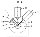
- FIG. 1 is a schematic diagram of a charged particle beam apparatus according to the present embodiment, which is drawn by seeing through a part of the inside of the apparatus.
- the charged particle beam apparatus includes an FIB column 3 that generates an ion beam for observing and processing the sample 1 and the probe 3, an SEM column 4 that generates an electron beam for observing the surface shape of the sample 1 and the probe 4, and a sample chamber 2. , A sample stage 5 on which the sample is placed, a probe driving unit for finely moving the probe in the sample chamber 2, a detector stage 6 for holding the detector 7, a deposition gas source, a display, and a calculation processing unit.
- the FIB column 3 can observe or process the surface of the sample 1 or the probe by irradiating the sample 1 or the probe with a beam of ions generated from the ion source. Further, the SEM column 4 can observe the surface of the sample 1 or the probe by irradiating the sample 1 or the probe with electrons generated from the electron source in the form of a beam. By arranging both columns so that the irradiation position of the electron beam from the SEM column 4 is substantially the same as the irradiation position of the ion beam from the FIB column 3, the processing portion by the ion beam is observed by the electron beam. be able to.
- the sample stage 5 can place the sample 1 and can be moved in a plane or rotationally. In addition, it is possible to move a position necessary for ion beam processing and observation to an ion beam irradiation position or to an electron beam observation position.
- the sample 1 in addition to a semiconductor sample, steel, light metal, polymer polymer, and the like are assumed.
- the probe can be moved in the sample chamber 2 by the probe driving unit, and is used to pick out a minute sample piece formed on the sample or to supply a potential to the sample by contacting the sample surface.
- the deposition gas source can store deposition gas that forms a deposited film by irradiation with a charged particle beam, and can supply it from the nozzle tip as necessary.
- the detector 7 is a detector for secondary electrons, secondary ions, backscattered electrons, X-rays, reflected electrons, transmitted electrons, and the like generated from an irradiation unit such as a sample or a probe by irradiation of an ion beam or an electron beam. These detection signals are processed and imaged by a calculation processing unit, and a secondary electron image, a secondary ion image, an element map by characteristic X-rays, a transmission electron image, and the like are displayed on a display.
- the calculation processing unit can control the FIB column 3, the SEM column 4, the detector 7, the detector stage 6, the sample stage 5, the deposition gas source, and the probe driving unit.
- the detector stage 6 includes a rotation mechanism, and the detector 7 can be disposed at a predetermined position.
- the detector 7 can rotate around the sample 1 with the normal line of the plane formed by the SEM column 4 and the FIB column 3 as a rotation axis.
- the posture of the sample 1 can be controlled by the plane movement or the rotational movement of the sample stage 5, the sample surface of the sample 1 faces the SEM column 4 in this embodiment. Further, the sample 1 is thinned so that transmitted electrons can be detected. Then, the rotation mechanism of the detector stage 6 is controlled by the calculation processing unit, the detector 7 is disposed at a position corresponding to the SEM column 4 with the sample stage 5 interposed therebetween, the optical axis of the SEM column 4, and the detector The main shaft is arranged in a straight line. The detector may be arranged at any location where electrons or the like that have passed through the sample 1 are strongly detected.
- the electron beam 9 generated in the SEM column 4 is incident on and scanned on the sample 1.
- the transmitted electrons of the sample 1 are detected by the detector 7 moving to a position on the electron beam axis, and a transmitted electron image of the sample is obtained by signal processing.
- the detector 7 is arranged on the upper left side of the paper surface by the detector stage 6, and is located where the sample surface of the sample 1 can be seen.
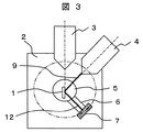
- the sample stage 5 is adjusted so that the sample surface of the sample 1 faces the direction of the FIB column 3. That is, the detector 7, the FIB column 3, and the SEM column 4 are arranged on the same side with respect to the sample surface, and the optical axis of the SEM column 4 and the main axis of the detector are the light of the FIB column 3. It arrange
- the detector may be disposed at any location where secondary electrons emitted from the sample 1 are strongly detected.
- the electron beam 9 generated in the SEM column 4 is incident on and scanned on the sample 1, and a signal 12 that is mainly secondary electrons is detected by the detector 7.
- SEM observation can be performed without directing the sample surface of the sample 1 in the direction of the SEM column 4 during the FIB processing / observation.
- the position of the detector 7 can be finely adjusted by the rotation mechanism of the detector stage 6, it is possible to detect a signal with an optimal arrangement according to the sample surface direction, the sample shape and the like.
- the sample stage 5 is adjusted so that the sample surface of the sample 1 is parallel to the FIB column 3.
- the detector 7 is arranged at the lower right side of the paper surface by the detector stage 6 and is located where the sample surface of the sample 1 can be seen. That is, the detector 7 and the SEM column 4 are arranged on the same side with respect to the sample surface, and the optical axis of the SEM column 4 and the main axis of the detector are in the normal line of the sample surface passing through the sample stage 5. It arrange
- the detector may be disposed at any location where secondary electrons emitted from the sample 1 are strongly detected.
- the electron beam 9 generated in the SEM column 4 is incident on and scanned on the sample 1, and a signal 12 that is mainly secondary electrons is detected by the detector 7.
- the sample surface of the sample 1 can be observed with an SEM while the sample 1 is thinned by focused ion beam irradiation.
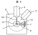
- FIG. 4 shows an example in which a signal generated by irradiation of an ion beam such as secondary ions or secondary electrons is detected.
- a detector 7 is arranged on the right side of the drawing sheet by the detector stage 6.
- the sample stage 5 is adjusted so that the sample surface of the sample 1 faces the direction of the SEM column 4.
- the FIB column 3 and the detector 7 are arranged so that the sample surface of the sample 1 can be seen.
- the optical axis of the FIB column 3 and the main axis of the detector are relative to the normal of the sample surface. Are arranged in line symmetry. It should be noted that the detector may be disposed at any location where secondary ions emitted from the sample 1 are strongly detected.
- the ion beam 10 generated in the FIB column 3 is incident on and scanned on the sample 1, and a signal 12 that is mainly secondary ions is detected by the detector 7.
- the optimum position for signal detection determined by the direction and shape of the sample can be adjusted. Further, only desired detection signals such as reflected electrons and transmitted electrons can be selectively acquired.
- the FIB column 3 is arranged vertically and the SEM column 4 is inclined, but this is not restrictive, and the FIB column 3 is arranged inclined and the SEM column 4 is arranged vertically. May be. Further, both the FIB column 3 and the SEM column 4 may be inclined. Further, a triple column configuration including a Ga focused ion beam column, an Ar focused ion beam column, and an electron beam column may be employed. Further, the rotational movement of the detector 7 is not limited to a system that can make one or more rotations, but may be a system that moves like a pendulum within a predetermined range, for example. Further, the arrangement of the detector 7 may be realized by combining not only rotational movement around the sample stage 5 but also vertical and horizontal movement and inclination angle change.
- a mechanism capable of moving the detector in the direction of the rotation radius in other words, a mechanism capable of changing the rotation radius, is added to the rotation mechanism of the detector stage 6 described in the first embodiment.
- a mechanism capable of changing the rotation radius is added to the rotation mechanism of the detector stage 6 described in the first embodiment.
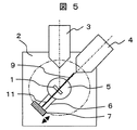
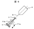
- FIG. 5 shows an outline of the charged particle beam apparatus of this example.
- transmitted electrons are detected by the same method as in the first embodiment, but the relative distance between the sample 1 and the detector 7 can be changed by a moving mechanism in the rotational radius direction added to the detector stage 6. .
- Fig. 6 shows the principle of detection of transmitted electrons.
- the electron beam 9 generated in the SEM column 4 is incident on and scanned on the sample 1, and the transmitted electrons 11 are detected by the detector 7.
- the transmitted electrons are classified into two types: bright-field transmitted electrons 11a that pass through the sample without much scattering, and dark-field transmitted electrons 11b that are scattered and transmitted inside the sample, and are divided by a sensor inside the detector. Detected individually. Among these, the latter dark-field transmitted electrons 11b change the detection angle of scattered electrons when the distance from the sample is changed by the detector stage 6, so that the detection angle is increased by moving the sample stage 7 away from the sample 1. Z contrast observation can be performed.
- the optimum signal intensity is obtained by bringing the detector 7 closer to the sample 1 and adjusting the distance between the detector 7 and the sample 1. be able to.
- a retraction mechanism in the rotation axis direction is added to the rotation mechanism in the rotation and rotation radius direction of the detector stage 6 described in the first and second embodiments.
- the difference from the first and second embodiments will be mainly described.
- FIG. 7 shows an outline of the charged particle beam apparatus of this example.
- This embodiment is a third embodiment.
- the detector of the present embodiment can move between the observation position and the retracted position.
- the detector 7 a exists on a plane including the optical axes of the FIB column 3 and the SEM column and the sample stage 5.
- the detector 7b exists near the wall on the opposite side of the wall of the sample chamber 2 to which the sample stage 5 and the deposition gas gun 8 are attached.
- a deposition gas gun 8 for discharging a deposition gas supplied from a deposition gas source to a predetermined position in a sample chamber is added for the purpose of forming a protective film during FIB processing, connecting a sample piece and a probe, and the like.
- the ambient environment when depositing the deposition gas is in a state where contamination due to gas is likely to occur.
- the performance of the detector 7 can be prevented from being deteriorated due to contamination by temporarily retracting the detector 7 in the direction away from the sample by the retracting mechanism. Further, when the detector stage 6 is moved, the detector 7 is retracted to the sample chamber side by the retracting mechanism, thereby preventing interference with other units such as the sample stage, the SEM lens barrel, and the FIB lens barrel. Can do.
Abstract
Il est possible de détecter un signal de détection à une position optimale lorsque le plan d'un échantillon est incliné par rapport à un faisceau de particules chargées. La présente invention a trait à un dispositif à faisceaux de particules chargées qui applique un faisceau de particules chargées à un échantillon tout en déplaçant un détecteur vers une pluralité de positions souhaitées autour d'un échantillon de manière à optimiser la position du détecteur. De la sorte, il est possible d'obtenir un signal de détection optimal en fonction de la posture et de la forme de l'échantillon, ce qui permet de procéder à une observation très précise d'échantillon telle qu'une observation par MEB, une observation par METB et une observation par FIB. De plus, dans le dispositif FIB/MEB, il est possible de détecter avec une très grande précision le point final du processus FIB.
Priority Applications (1)
| Application Number | Priority Date | Filing Date | Title |
|---|---|---|---|
| US13/202,554 US8610060B2 (en) | 2009-02-27 | 2009-10-23 | Charged particle beam device |
Applications Claiming Priority (2)
| Application Number | Priority Date | Filing Date | Title |
|---|---|---|---|
| JP2009045048A JP5103422B2 (ja) | 2009-02-27 | 2009-02-27 | 荷電粒子ビーム装置 |
| JP2009-045048 | 2009-02-27 |
Publications (1)
| Publication Number | Publication Date |
|---|---|
| WO2010097861A1 true WO2010097861A1 (fr) | 2010-09-02 |
Family
ID=42665088
Family Applications (1)
| Application Number | Title | Priority Date | Filing Date |
|---|---|---|---|
| PCT/JP2009/005581 WO2010097861A1 (fr) | 2009-02-27 | 2009-10-23 | Dispositif à faisceaux de particules chargées |
Country Status (3)
| Country | Link |
|---|---|
| US (1) | US8610060B2 (fr) |
| JP (1) | JP5103422B2 (fr) |
| WO (1) | WO2010097861A1 (fr) |
Families Citing this family (15)
| Publication number | Priority date | Publication date | Assignee | Title |
|---|---|---|---|---|
| JP5612493B2 (ja) * | 2010-03-18 | 2014-10-22 | 株式会社日立ハイテクサイエンス | 複合荷電粒子ビーム装置 |
| DE102010024625A1 (de) * | 2010-06-22 | 2011-12-22 | Carl Zeiss Nts Gmbh | Verfahren zum Bearbeiten eines Objekts |
| JP5690086B2 (ja) * | 2010-07-02 | 2015-03-25 | 株式会社キーエンス | 拡大観察装置 |
| JP5517790B2 (ja) * | 2010-07-02 | 2014-06-11 | 株式会社キーエンス | 拡大観察装置 |
| DE102011006588A1 (de) * | 2011-03-31 | 2012-10-04 | Carl Zeiss Nts Gmbh | Teilchenstrahlgerät mit Detektoranordnung |
| KR101843042B1 (ko) * | 2012-01-11 | 2018-03-28 | 삼성전자주식회사 | 반도체 기판 검사 장비 및 이를 이용한 반도체 기판 검사 방법 |
| JP5852474B2 (ja) * | 2012-03-01 | 2016-02-03 | 株式会社日立ハイテクノロジーズ | 荷電粒子線装置 |
| EP2722866A1 (fr) * | 2012-10-22 | 2014-04-23 | Fei Company | Appareil configurable à fiasceau de particules chargées |
| JP5856574B2 (ja) * | 2013-02-13 | 2016-02-10 | 株式会社東芝 | 試料加工方法 |
| EP2816585A1 (fr) * | 2013-06-17 | 2014-12-24 | ICT Integrated Circuit Testing Gesellschaft für Halbleiterprüftechnik mbH | Système à faisceau de particules chargées et son procédé de fonctionnement |
| WO2015118605A1 (fr) * | 2014-02-04 | 2015-08-13 | 富士通株式会社 | Dispositif et procédé d'évaluation de matériau |
| US10354836B2 (en) * | 2014-03-09 | 2019-07-16 | Ib Labs, Inc. | Methods, apparatuses, systems and software for treatment of a specimen by ion-milling |
| US11024481B2 (en) * | 2016-03-04 | 2021-06-01 | Fei Company | Scanning electron microscope |
| JP2017198588A (ja) * | 2016-04-28 | 2017-11-02 | 株式会社ニューフレアテクノロジー | パターン検査装置 |
| US11094501B2 (en) * | 2019-11-19 | 2021-08-17 | ICT Integrated Circuit Testing Gesellschaft für Halbleiterprüftechnik mbH | Secondary charged particle imaging system |
Citations (3)
| Publication number | Priority date | Publication date | Assignee | Title |
|---|---|---|---|---|
| JPS56132756A (en) * | 1980-03-19 | 1981-10-17 | Hitachi Ltd | Secondary electron detector |
| JPS59201356A (ja) * | 1983-04-30 | 1984-11-14 | Shimadzu Corp | 走査型電子顕微鏡 |
| JP2008210702A (ja) * | 2007-02-27 | 2008-09-11 | Hitachi High-Technologies Corp | 荷電粒子ビーム装置及び印加電圧制御方法 |
Family Cites Families (8)
| Publication number | Priority date | Publication date | Assignee | Title |
|---|---|---|---|---|
| JP4178741B2 (ja) | 2000-11-02 | 2008-11-12 | 株式会社日立製作所 | 荷電粒子線装置および試料作製装置 |
| JP2004039453A (ja) * | 2002-07-03 | 2004-02-05 | Seiko Instruments Inc | 微細ステンシル構造修正装置 |
| US7834315B2 (en) * | 2007-04-23 | 2010-11-16 | Omniprobe, Inc. | Method for STEM sample inspection in a charged particle beam instrument |
| US8835845B2 (en) * | 2007-06-01 | 2014-09-16 | Fei Company | In-situ STEM sample preparation |
| JP5352335B2 (ja) * | 2009-04-28 | 2013-11-27 | 株式会社日立ハイテクノロジーズ | 複合荷電粒子線装置 |
| JP5612493B2 (ja) * | 2010-03-18 | 2014-10-22 | 株式会社日立ハイテクサイエンス | 複合荷電粒子ビーム装置 |
| JP5690086B2 (ja) * | 2010-07-02 | 2015-03-25 | 株式会社キーエンス | 拡大観察装置 |
| JP5517790B2 (ja) * | 2010-07-02 | 2014-06-11 | 株式会社キーエンス | 拡大観察装置 |
-
2009
- 2009-02-27 JP JP2009045048A patent/JP5103422B2/ja active Active
- 2009-10-23 US US13/202,554 patent/US8610060B2/en not_active Expired - Fee Related
- 2009-10-23 WO PCT/JP2009/005581 patent/WO2010097861A1/fr active Application Filing
Patent Citations (3)
| Publication number | Priority date | Publication date | Assignee | Title |
|---|---|---|---|---|
| JPS56132756A (en) * | 1980-03-19 | 1981-10-17 | Hitachi Ltd | Secondary electron detector |
| JPS59201356A (ja) * | 1983-04-30 | 1984-11-14 | Shimadzu Corp | 走査型電子顕微鏡 |
| JP2008210702A (ja) * | 2007-02-27 | 2008-09-11 | Hitachi High-Technologies Corp | 荷電粒子ビーム装置及び印加電圧制御方法 |
Also Published As
| Publication number | Publication date |
|---|---|
| JP2010199002A (ja) | 2010-09-09 |
| US8610060B2 (en) | 2013-12-17 |
| JP5103422B2 (ja) | 2012-12-19 |
| US20110297827A1 (en) | 2011-12-08 |
Similar Documents
| Publication | Publication Date | Title |
|---|---|---|
| JP5103422B2 (ja) | 荷電粒子ビーム装置 | |
| EP3428950B1 (fr) | Procédé d'alignement d'un faisceau lumineux sur un faisceau de particules chargées et système de faisceau de particules chargées | |
| US9733164B2 (en) | Lamella creation method and device using fixed-angle beam and rotating sample stage | |
| JP5142240B2 (ja) | 荷電ビーム装置及び荷電ビーム加工方法 | |
| KR102056507B1 (ko) | 하전 입자 빔 장치 및 시료 관찰 방법 | |
| JP4769828B2 (ja) | 荷電粒子ビーム装置 | |
| EP2610891B1 (fr) | Dispositif de faisceau de particules chargées, et procédé d'observation d'échantillon | |
| US9793122B2 (en) | Combined laser processing system and focused ion beam system | |
| JP5378185B2 (ja) | 集束イオンビーム装置、及び集束イオンビーム加工方法 | |
| JP4654216B2 (ja) | 荷電粒子線装置用試料ホールダ | |
| KR102169574B1 (ko) | 하전 입자 빔 장치 | |
| CN102779713B (zh) | 带检测器装置的粒子束仪 | |
| US8642980B2 (en) | Composite charged particle beam apparatus | |
| US20120006786A1 (en) | Method and system for preparing a sample | |
| US11087953B2 (en) | Moveable detector | |
| JP2018022592A (ja) | 試料台およびそれを備えた電子顕微鏡 | |
| EP3973559B1 (fr) | Diffractomètre pour cristallographie à particules chargées | |
| JP4845452B2 (ja) | 試料観察方法、及び荷電粒子線装置 | |
| JP6316453B2 (ja) | 荷電粒子線装置及び荷電粒子線装置による観察方法 | |
| US11094503B2 (en) | Method of preparing thin film sample piece and charged particle beam apparatus | |
| JP2016051591A (ja) | 荷電粒子ビーム装置 | |
| JP2011233249A (ja) | イオンビーム照射位置決め装置 |
Legal Events
| Date | Code | Title | Description |
|---|---|---|---|
| 121 | Ep: the epo has been informed by wipo that ep was designated in this application |
Ref document number: 09840715 Country of ref document: EP Kind code of ref document: A1 |
|
| WWE | Wipo information: entry into national phase |
Ref document number: 13202554 Country of ref document: US |
|
| NENP | Non-entry into the national phase |
Ref country code: DE |
|
| 122 | Ep: pct application non-entry in european phase |
Ref document number: 09840715 Country of ref document: EP Kind code of ref document: A1 |