WO2010095658A1 - 微細結晶-アモルファス混在金合金およびめっき皮膜、そのためのめっき液およびめっき皮膜形成方法 - Google Patents
微細結晶-アモルファス混在金合金およびめっき皮膜、そのためのめっき液およびめっき皮膜形成方法 Download PDFInfo
- Publication number
- WO2010095658A1 WO2010095658A1 PCT/JP2010/052364 JP2010052364W WO2010095658A1 WO 2010095658 A1 WO2010095658 A1 WO 2010095658A1 JP 2010052364 W JP2010052364 W JP 2010052364W WO 2010095658 A1 WO2010095658 A1 WO 2010095658A1
- Authority
- WO
- WIPO (PCT)
- Prior art keywords
- plating film
- amorphous
- gold alloy
- gold
- film according
- Prior art date
- Legal status (The legal status is an assumption and is not a legal conclusion. Google has not performed a legal analysis and makes no representation as to the accuracy of the status listed.)
- Ceased
Links
Images







Classifications
-
- C—CHEMISTRY; METALLURGY
- C25—ELECTROLYTIC OR ELECTROPHORETIC PROCESSES; APPARATUS THEREFOR
- C25D—PROCESSES FOR THE ELECTROLYTIC OR ELECTROPHORETIC PRODUCTION OF COATINGS; ELECTROFORMING; APPARATUS THEREFOR
- C25D3/00—Electroplating: Baths therefor
- C25D3/02—Electroplating: Baths therefor from solutions
- C25D3/56—Electroplating: Baths therefor from solutions of alloys
- C25D3/62—Electroplating: Baths therefor from solutions of alloys containing more than 50% by weight of gold
-
- C—CHEMISTRY; METALLURGY
- C25—ELECTROLYTIC OR ELECTROPHORETIC PROCESSES; APPARATUS THEREFOR
- C25D—PROCESSES FOR THE ELECTROLYTIC OR ELECTROPHORETIC PRODUCTION OF COATINGS; ELECTROFORMING; APPARATUS THEREFOR
- C25D5/00—Electroplating characterised by the process; Pretreatment or after-treatment of workpieces
- C25D5/60—Electroplating characterised by the structure or texture of the layers
- C25D5/615—Microstructure of the layers, e.g. mixed structure
-
- C—CHEMISTRY; METALLURGY
- C25—ELECTROLYTIC OR ELECTROPHORETIC PROCESSES; APPARATUS THEREFOR
- C25D—PROCESSES FOR THE ELECTROLYTIC OR ELECTROPHORETIC PRODUCTION OF COATINGS; ELECTROFORMING; APPARATUS THEREFOR
- C25D7/00—Electroplating characterised by the article coated
Definitions
- the present invention has been made in view of the above circumstances, and has a fine crystal-amorphous mixed gold alloy plating film excellent in wear resistance and having good conductivity and chemical stability and improved hardness, and this fine crystal-amorphous
- An object is to provide an electroplating solution capable of forming a mixed gold alloy plating film and an electroplating method using the electroplating solution.
- a complex electroplating solution containing a complexing agent such as an organic acid, an inorganic acid or a salt thereof and ammonia or ammonium ions the solution is excellent
- a microcrystalline-amorphous mixed gold alloy plating film formed by mixing a microcrystalline phase and an amorphous phase can be obtained, and this film has a good resistivity value and chemical stability inherent in gold.
- the present inventors have completed the present invention.
- the present invention provides (1) a fine crystal-amorphous mixed gold alloy plating film characterized by being formed by mixing a fine crystal phase and an amorphous phase, and (2) a gold cyanide salt having a gold standard of 0 .0001-0.4 mol / dm 3 concentration, nickel salt concentration of 0.001-0.5 mol / dm 3 on nickel basis, and / or cobalt salt concentration of 0.001-0.5 mol / dm 3 on cobalt basis.
- a complexing agent such as an organic acid, an inorganic acid or a salt thereof is added at a concentration of 0.001 to 2.0 mol / dm 3
- ammonia or ammonium ions are added at a concentration of 0.001 to 5.0 mol / liquid stability good electroplating solution, characterized in that it contains a concentration of dm 3, and (3) the electroplating solution to be plated onto the fine crystals with - amorphous mixed gold alloy Providing an electroplating method and forming the Kki film.
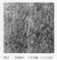
- FIG. 4 is a diagram showing a TEM image (1,000,000 times) of a fine crystal-amorphous mixed gold alloy plating film obtained in Example 2.
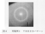
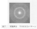
- FIG. 4 is a diagram showing a THEED pattern of a fine crystal-amorphous mixed gold alloy plating film obtained in Example 2.
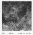
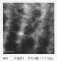
- FIG. 4 is a diagram showing a TEM image (300,000 times) of a fine crystal-amorphous mixed gold alloy plating film obtained in Example 3.
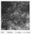
- FIG. 4 is a diagram showing a TEM image (1,000,000 times) of a fine crystal-amorphous mixed gold alloy plating film obtained in Example 3.
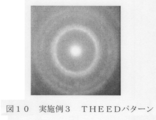
- FIG. 4 is a diagram showing a THEED pattern of a fine crystal-amorphous mixed gold alloy plating film obtained in Example 3.
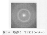
- FIG. 6 is a diagram showing a THEED pattern of a fine crystal-amorphous mixed gold alloy plating film obtained in Example 5.
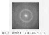
- FIG. It is a figure which shows the TEM image (1,000,000 times) of the amorphous gold alloy plating film obtained by the comparative example 1. It is a figure which shows the THEED pattern of the amorphous gold alloy plating film obtained by the comparative example 1.
- the fine crystal-amorphous mixed gold alloy plating film of the present invention contains nickel and / or cobalt in gold, and the fine structure is a structure in which a fine crystal phase and an amorphous phase are mixed. High hardness is achieved with good specific resistance and chemical stability compared to an amorphous gold alloy plating film with an amorphous structure.
- Such a structure in which a fine crystal phase and an amorphous phase are mixed can be confirmed by an X-ray diffraction (XRD) pattern, a transmission electron microscope (TEM) image, and a transmission high energy electron diffraction (THEED) image.
- the average particle size of the fine crystals is preferably 30 nm or less, particularly 20 nm or less, and more preferably 15 nm or less from the viewpoint of maintaining high hardness.
- the fine crystal-amorphous mixed gold alloy plating film of the present invention has a characteristic of maintaining the original characteristics (good resistivity and chemical stability) of gold or high hardness not found in conventional gold or gold alloy plating films. Therefore, the volume fraction of the fine crystals is preferably 10 to 90%, particularly 15 to 60%.
- the Knoop hardness is Hk 180 or more, particularly Hk 220 or more, further Hk 300 or more, particularly Hk 350 or more, and the specific resistance is 200 ⁇ ⁇ cm or less, particularly 150 ⁇ ⁇ cm or less, particularly 100 ⁇ ⁇ cm or less.
- a fine crystal-amorphous mixed gold alloy plating film having high hardness and specific resistance can be obtained. Further, in the fine crystal-amorphous mixed gold alloy plating film of the present invention, the structure in which the fine crystal phase and the amorphous phase are mixed is changed by annealing at 300 ° C. or lower (held for 1 hour) (that is, crystallization occurs). The average grain size and volume fraction of the fine crystals will not increase).
- the electroplating solution contains a gold cyanide salt, a nickel salt and / or a cobalt salt.
- the gold cyanide salt include nickel gold cyanide, sodium gold cyanide, lithium gold cyanide and the like.
- Specific examples of the salt include nickel sulfate and nickel nitrate, and specific examples of the cobalt salt include cobalt sulfate and cobalt nitrate.
- the gold cyanide salt concentration in the plating solution is 0.0001 to 0.4 mol / dm 3 , preferably 0.001 to 0.2 mol / dm 3 , more preferably 0.01 to 0.1 mol / dm 3 on a gold basis.
- the pH of the electroplating solution is preferably 3 to 11, particularly 5 to 9, and particularly around pH 6.
- a conventionally known pH adjuster such as aqueous ammonia or potassium hydroxide can be used.
- this electroplating solution has no significant influence on the film physical properties (volume fraction and average particle diameter of fine crystals, peak half width of XRD pattern, Knoop hardness, specific resistance) and film composition of the plating film.
- surfactants, solvents, etc. for purposes such as improving glossiness, preventing pits, imparting conductivity, imparting buffering properties, expanding the usable current density range, promoting precipitation rate, improving heat resistance, improving wettability, etc. (See, for example, JP-A-7-11476, JP-A-2004-76026, and JP-A-2006-37164).
- the electroplating conditions are not particularly limited, but the plating temperature is preferably 20 to 95 ° C, particularly 50 to 90 ° C.
- Cathode current density vary with the composition of the plating solution, it is not particularly limited, low current density range (e.g. 1 mA / cm 2 or more 10 mA / cm less than 2) and a high current density range (e.g. 10 mA / cm 2 than
- the fine crystal-amorphous mixed gold alloy plating film can be obtained at both of 200 mA / cm 2 or less.
- an insoluble anode such as platinum can be used for the anode.
- Nickel and / or cobalt may be used as the anode.
- examples of the object to be plated include metal materials such as copper and nickel used for electric wiring and the like. This metal material may be formed as a base layer on a metal substrate or a non-metal substrate.
- this metal material may be formed as a base layer on a metal substrate or a non-metal substrate.
- a fine crystal-amorphous mixed gold alloy plating film (film thickness: 1 ⁇ m) was formed on a copper plate having a temperature of 70 ° C. and a current density of 10 mA / cm 2 and a purity of 99.96%.
- a platinum-coated titanium electrode (network) was used as the anode, and the plating bath during plating was vigorously stirred.
- the obtained fine crystal-amorphous mixed gold alloy plating film was analyzed by XRD, TEM and THEED.
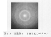
- An XRD pattern is shown in FIG. 1, and a TEM image and a THEED pattern are shown in FIGS.
- the TEM image it is possible to observe a mixture of crystal stripes peculiar to crystals and irregular structures peculiar to amorphous.
- the THEED pattern it can be observed that a diffraction spot peculiar to crystal and a halo ring peculiar to amorphous are mixed.
- the obtained plating film has a fine crystal-amorphous mixed structure.
- the average grain size of the fine crystals was 10 nm, and the volume fraction of the fine crystal phase was 50%.
- composition analysis, Knoop hardness and specific resistance of the obtained fine crystal-amorphous mixed gold alloy plating film were measured. Gold was detected at a content of 41.2 atomic percent as a metallic element, 46.0 atomic percent of nickel, and 12.8 atomic percent of carbon as a nonmetallic element. The Knoop hardness was Hk347, and the specific resistance was 89 ⁇ ⁇ cm.
- Plating was conducted in the same manner as in Example 1 except that 20 vol% of n-propanol was added, and XRD, TEM and THEED analysis was performed on the obtained plating film.
- An XRD pattern is shown in FIG. 1, and a TEM image and a THEED pattern are shown in FIGS.
- the TEM image it is possible to observe a mixture of crystal stripes peculiar to crystals and irregular structures peculiar to amorphous.
- the obtained plating film has a fine crystal-amorphous mixed structure.
- the average grain size of the fine crystals was 10 nm, and the volume fraction of the fine crystal phase was 50%.
- composition analysis, Knoop hardness and specific resistance of the obtained fine crystal-amorphous mixed gold alloy plating film were measured. Gold was detected at a content of 48.1 atomic% as a metallic element, 38.1 atomic% of nickel, and 13.8 atomic% of carbon as a nonmetallic element. The Knoop hardness was Hk348, and the specific resistance was 89 ⁇ ⁇ cm.
- the citric acid concentration was 0.143 mol / dm 3
- the ammonia concentration was 1.2 mol / dm 3
- current density was 1 mA / cm 2 (energization time 50 seconds) and 10 mA / cm 2 (energization time 5 seconds), without intermission.
- Plating was performed in the same manner as in Example 1 except that the electrolytic plating was alternately performed, and XRD, TEM and THEED analysis was performed on the obtained plating film. An XRD pattern is shown in FIG. 1, and a TEM image and a THEED pattern are shown in FIGS.
- the plating film obtained by pulse plating has a fine crystal-amorphous mixed structure. Further, as a result of observing the TEM image, the average particle diameter of the fine crystals was 10 nm, and the volume fraction of the fine crystal phase was 60%. On the other hand, composition analysis, Knoop hardness and specific resistance of the obtained plating film were measured. Gold was detected at a content of 47.4 atomic% as a metallic element, 47.0 atomic% of nickel, and 5.6 atomic% as a nonmetallic element. The Knoop hardness was Hk222, and the specific resistance was 57 ⁇ ⁇ cm.
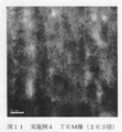
- XRD, TEM, and THEED analyzes were performed on the plating film obtained by annealing the film at an annealing temperature (heat retention temperature) of 400 ° C., a temperature increase rate of 10 ° C./min, and a heat retention of 1 hour in an air atmosphere.
- An XRD pattern is shown in FIG. 1, and a TEM image and a THEED pattern are shown in FIGS.
- KAu (CN) 2 is contained in 0.035 mol / dm 3
- CoSO 4 .7H 2 O is contained in 0.076 mol / dm 3
- citric acid / H 2 O is contained in 0.1 mol / dm 3
- the ammonia concentration is 0.44 mol / dm 3. and dm 3, with KOH and electroplating solution and the pH was adjusted to 6 with sulfuric acid, the temperature 70 ° C., a current density of 10 mA / cm 2 with a purity 99.96% of the copper plate on the microcrystalline - amorphous mixed gold alloy plated film ( A film thickness of 1 ⁇ m) was formed.
- a platinum-coated titanium electrode (network) was used as the anode, and the plating bath during plating was vigorously stirred.
- the obtained fine crystal-amorphous mixed gold alloy plating film was analyzed by XRD, TEM and THEED.
- An XRD pattern is shown in FIG. 1, and a TEM image and a THEED pattern are shown in FIGS.
- the TEM image it is possible to observe a mixture of crystal stripes peculiar to crystals and irregular structures peculiar to amorphous.
- the THEED pattern it can be observed that a diffraction spot peculiar to crystal and a halo ring peculiar to amorphous are mixed.
- the obtained plating film has a fine crystal-amorphous mixed structure.
- the average grain size of the fine crystals was 5 nm, and the volume fraction of the fine crystal phase was 15%.
- composition analysis and Knoop hardness of the obtained fine crystal-amorphous mixed gold alloy plating film were measured. Gold was detected at a content of 36.4 atomic% as a metallic element, 40.6 atomic% of cobalt, and 23.0 atomic% of carbon as a nonmetallic element. Knoop hardness was Hk180.
- the obtained plating film has a homogeneous amorphous structure having no fine crystals.
- composition analysis, Knoop hardness and specific resistance of the obtained plating film were measured. Gold was detected at a content of 15.2 atomic% as a metal element, 67.5 atomic% as a nickel element, and 17.3 atomic% as a nonmetallic element. The Knoop hardness was Hk435, and the specific resistance was 251 ⁇ ⁇ cm.
- KAu (CN) 2 contains 0.04 mol / dm 3
- NiSO 4 .6H 2 O contains 0.0085 mol / dm 3
- citric acid / H 2 O contains 0.5 mol / dm 3
- KOH contains 0.7 mol / dm 3
- the obtained hard gold plating film was analyzed by XRD, TEM and THEED.
- the XRD pattern is shown in FIG.
- the average particle diameter of the crystal was 13 nm.
- composition analysis, Knoop hardness and specific resistance of the obtained plating film were measured.
- Gold was detected as a metal element at a content of 96.5 atomic%, nickel as a 0.77 atomic%, and carbon as a nonmetallic element at a content of 2.7 atomic%.
- the Knoop hardness was Hk160, and the specific resistance was 17 ⁇ ⁇ cm.
- the Knoop hardness of the fine crystal-amorphous mixed gold alloy plating film of Example 1 is that of additive-free hard gold (AFHG), nickel hard gold (NiHG), and CoHG, which are considered to have high hardness in the gold plating film. It can be seen that the Knoop hardness does not reach Hk200, but has a high hardness corresponding to 2 to 3 times.
Landscapes
- Chemical & Material Sciences (AREA)
- Engineering & Computer Science (AREA)
- Chemical Kinetics & Catalysis (AREA)
- Electrochemistry (AREA)
- Materials Engineering (AREA)
- Metallurgy (AREA)
- Organic Chemistry (AREA)
- Crystallography & Structural Chemistry (AREA)
- Electroplating And Plating Baths Therefor (AREA)
- Electroplating Methods And Accessories (AREA)
Abstract
Description
本発明の微細結晶-アモルファス混在金合金めっき皮膜は、微細結晶相とアモルファス相が混在して形成されている。
理学電機社製 RINT2100‐Ultima+による:XRD法 CuKα(40kV/40mA)
または、日立ハイテクノロイジーズ社製 HF-2200による:TEM及びTHEED法 加速電圧200V 明視野像
体積分率
日立ハイテクノロイジーズ社製 HF-2200による:TEM法及びTHEED法 加速電圧200V 明視野像
金属組成
エスアイアイ・ナノテクノロジー社製 SEA5100による:EDXRF法
非金属元素測定
堀場製作所社製 EMIA-920V、米国LECO社製 TC-436による
ヌープ硬さ
JIS Z 2251に準じて測定:荷重5gf 荷重保持時間30秒 銅板上に形成された30μm厚みのめっき皮膜で測定した
比抵抗
共和理研社製 K-705RSによる:JIS K 7194に準じて測定(四探針法)
くえん酸濃度を0.143mol/dm3、アンモニア濃度を0.46mol/dm3とした以外は、実施例1と同様にめっきを行い、得られためっき皮膜についてXRD、TEM及びTHEED分析を行った。XRDパターンを図1に、TEM像及びTHEEDパターンを図17~18に示す。XRDパターンの2θ=40度付近にはアモルファス特有のピーク半値幅1度以上のブロードピークが確認できる。また、TEM像にはアモルファス特有の不規則構造が確認でき、結晶粒界や結晶縞のような規則的構造は確認できなかった。そして、THEEDパターンにはアモルファス特有のハローリングが確認できる。この結果から、得られためっき皮膜は、微細結晶を有さない均質なアモルファス構造をとっていることがわかる。また、得られためっき皮膜の組成分析、ヌープ硬さ及び比抵抗を測定した。金属元素として金が15.2原子%、ニッケルが67.5原子%、非金属元素として炭素が17.3原子%の含有率で検出された。ヌープ硬さはHk435、比抵抗は251μΩ・cmであった。
KAu(CN)2を0.04mol/dm3、NiSO4・6H2Oを0.0085mol/dm3、くえん酸・H2Oを0.5mol/dm3、KOHを0.7mol/dm3含有し、硫酸によりpHを3.5に調整した電気めっき液を用い、温度30℃、電流密度10mA/cm2で純度99.96%の銅板上に硬質金めっき皮膜(膜厚1μm)を形成した。なお、アノードには白金被覆チタン電極(網状)を用い、めっき中のめっき浴は緩やかに撹拌した。
Claims (13)
- 金合金のめっき皮膜であって、結晶相とアモルファス相とが混在して形成されてなる、前記めっき皮膜。
- 結晶相の体積分率が10~90%である、請求項1に記載のめっき皮膜。
- 結晶相の平均粒径が30nm以下である、請求項1に記載のめっき皮膜。
- X線回折パターンにおける2θ=40度付近のピーク半値幅が1度以上である、請求項1記載のめっき皮膜。
- ヌープ硬さがHk180以上である、請求項1~4のいずれかに記載のめっき皮膜。
- 比抵抗が200μΩ・cm以下である、請求項1~5のいずれかに記載のめっき皮膜。
- 組成式:Au100-x-yMx Cy(ここにおいてはAuまたはMが主成分であり、MはNiおよび/またはCoであり、Cは炭素であり、1原子%≦x≦80原子%、1原子%≦y≦30原子%である)で表される、請求項1~6のいずれかに記載のめっき皮膜。
- 電気接点材料として用いる、請求項1~7のいずれかに記載のめっき皮膜。
- 請求項1~8のいずれかに記載のめっき皮膜を形成するための電気めっき液であって、シアン化金塩、ニッケル塩および/またはコバルト塩、錯化剤およびpH調整剤を含む、前記電気めっき液。
- 錯化剤がくえん酸、酒石酸、りんご酸、ピロりん酸、りん酸、スルファミン酸およびそれらのナトリウム塩、カリウム塩、アンモニウム塩からなる群から選択される1または2以上であり、また、pH調整剤がアンモニア水または水酸化カリウムである、請求項9に記載の電気めっき液。
- 錯化剤がくえん酸であり、pH調整剤がアンモニア水である、請求項10に記載の電気めっき液。
- 金合金めっき皮膜の形成方法であって、請求項9~11のいずれかに記載の電気めっき液を用いて被めっき物上に結晶相とアモルファス相とが混在してなる金合金めっき皮膜を形成してなる、前記形成方法。
- 請求項1~8のいずれかに記載のめっき皮膜を用いた、電気・電子部品。
Priority Applications (3)
| Application Number | Priority Date | Filing Date | Title |
|---|---|---|---|
| DE112010000791T DE112010000791T5 (de) | 2009-02-17 | 2010-02-17 | Gemischt-mikrokristallin-amorphe goldlegierung uind elektrochemisch abgeschiedener film sowiebadlösung, und verfahren zur erzeugung eines elektrochemisch abgeschiedenen films für diese |
| US13/202,050 US20120031764A1 (en) | 2009-02-17 | 2010-02-17 | Microcrystalline-to-amorphous gold alloy and plated film, and plating solution for those, and plated film formation method |
| CN2010800080735A CN102317508A (zh) | 2009-02-17 | 2010-02-17 | 微晶-非晶混合金合金及镀膜、镀覆液及镀膜形成方法 |
Applications Claiming Priority (2)
| Application Number | Priority Date | Filing Date | Title |
|---|---|---|---|
| JP2009033632A JP5424666B2 (ja) | 2009-02-17 | 2009-02-17 | 微細結晶−アモルファス混在金合金およびめっき皮膜、そのためのめっき液およびめっき皮膜形成方法 |
| JP2009-033632 | 2009-02-17 |
Publications (1)
| Publication Number | Publication Date |
|---|---|
| WO2010095658A1 true WO2010095658A1 (ja) | 2010-08-26 |
Family
ID=42633938
Family Applications (1)
| Application Number | Title | Priority Date | Filing Date |
|---|---|---|---|
| PCT/JP2010/052364 Ceased WO2010095658A1 (ja) | 2009-02-17 | 2010-02-17 | 微細結晶-アモルファス混在金合金およびめっき皮膜、そのためのめっき液およびめっき皮膜形成方法 |
Country Status (7)
| Country | Link |
|---|---|
| US (1) | US20120031764A1 (ja) |
| JP (1) | JP5424666B2 (ja) |
| KR (1) | KR20110132356A (ja) |
| CN (1) | CN102317508A (ja) |
| DE (1) | DE112010000791T5 (ja) |
| TW (1) | TWI476301B (ja) |
| WO (1) | WO2010095658A1 (ja) |
Families Citing this family (5)
| Publication number | Priority date | Publication date | Assignee | Title |
|---|---|---|---|---|
| JP2012184468A (ja) * | 2011-03-04 | 2012-09-27 | Waseda Univ | めっき膜、電子部品、めっき液、および、めっき膜の製造方法 |
| JP5896508B2 (ja) * | 2011-04-28 | 2016-03-30 | 学校法人早稲田大学 | 組成物およびニッケル炭化物Ni3Cを主相とするめっき膜の製造用電気めっき液 |
| DE102017002472A1 (de) * | 2017-03-14 | 2018-09-20 | Diehl Metal Applications Gmbh | Steckverbinder |
| JP7409998B2 (ja) * | 2020-08-27 | 2024-01-09 | 日立Astemo株式会社 | 緩衝器および緩衝器の製造方法 |
| US20260015222A1 (en) * | 2024-07-12 | 2026-01-15 | Menlo Microsystems, Inc. | Two stage plating for reduced Ni and NiO layer formation |
Citations (2)
| Publication number | Priority date | Publication date | Assignee | Title |
|---|---|---|---|---|
| JP2000026989A (ja) * | 1998-07-10 | 2000-01-25 | Nau Chemical:Kk | Au−Sn箔の製造方法 |
| JP2007169706A (ja) * | 2005-12-21 | 2007-07-05 | Univ Waseda | アモルファス金−ニッケル系合金めっき皮膜形成用電気めっき液及び電気めっき方法 |
Family Cites Families (9)
| Publication number | Priority date | Publication date | Assignee | Title |
|---|---|---|---|---|
| JPS6033382A (ja) | 1983-08-03 | 1985-02-20 | Nippon Pureeteingu Kk | パルス電解による非晶質合金の電着方法 |
| JPS62290893A (ja) | 1986-06-09 | 1987-12-17 | Nippon Mining Co Ltd | 金−ニツケル合金めつき液及びめつき方法 |
| JPH0711476A (ja) | 1993-06-23 | 1995-01-13 | Kojima Kagaku Yakuhin Kk | パラジウムめっき液 |
| JP3989795B2 (ja) | 2002-08-09 | 2007-10-10 | エヌ・イーケムキャット株式会社 | 電解硬質金めっき液及びそれを用いためっき方法 |
| JP2004300483A (ja) | 2003-03-28 | 2004-10-28 | Asahi Kasei Chemicals Corp | 結晶質と非晶質組織から成る材料 |
| JP4614052B2 (ja) | 2004-07-27 | 2011-01-19 | 石原薬品株式会社 | ニッケルのバレルメッキ方法 |
| WO2006052866A1 (en) * | 2004-11-05 | 2006-05-18 | Tufts University | Treatment of ceria-based catalysts with oxygen to improve stability thereof in the water-gas shift and selective co oxidation reactions |
| JP4868123B2 (ja) | 2005-02-04 | 2012-02-01 | 学校法人早稲田大学 | 金−ニッケル系アモルファス合金めっき皮膜、電気めっき液及び電気めっき方法 |
| JP4868116B2 (ja) * | 2005-09-30 | 2012-02-01 | 学校法人早稲田大学 | 金−コバルト系アモルファス合金めっき皮膜、電気めっき液及び電気めっき方法 |
-
2009
- 2009-02-17 JP JP2009033632A patent/JP5424666B2/ja not_active Expired - Fee Related
-
2010
- 2010-02-17 US US13/202,050 patent/US20120031764A1/en not_active Abandoned
- 2010-02-17 DE DE112010000791T patent/DE112010000791T5/de not_active Withdrawn
- 2010-02-17 KR KR1020117020623A patent/KR20110132356A/ko not_active Withdrawn
- 2010-02-17 WO PCT/JP2010/052364 patent/WO2010095658A1/ja not_active Ceased
- 2010-02-17 CN CN2010800080735A patent/CN102317508A/zh active Pending
- 2010-02-22 TW TW099104998A patent/TWI476301B/zh not_active IP Right Cessation
Patent Citations (2)
| Publication number | Priority date | Publication date | Assignee | Title |
|---|---|---|---|---|
| JP2000026989A (ja) * | 1998-07-10 | 2000-01-25 | Nau Chemical:Kk | Au−Sn箔の製造方法 |
| JP2007169706A (ja) * | 2005-12-21 | 2007-07-05 | Univ Waseda | アモルファス金−ニッケル系合金めっき皮膜形成用電気めっき液及び電気めっき方法 |
Also Published As
| Publication number | Publication date |
|---|---|
| JP2010189685A (ja) | 2010-09-02 |
| TWI476301B (zh) | 2015-03-11 |
| TW201111560A (en) | 2011-04-01 |
| US20120031764A1 (en) | 2012-02-09 |
| KR20110132356A (ko) | 2011-12-07 |
| CN102317508A (zh) | 2012-01-11 |
| DE112010000791T5 (de) | 2012-07-26 |
| JP5424666B2 (ja) | 2014-02-26 |
Similar Documents
| Publication | Publication Date | Title |
|---|---|---|
| EP2749673B1 (en) | Silver plating and production method therefor | |
| JP5424666B2 (ja) | 微細結晶−アモルファス混在金合金およびめっき皮膜、そのためのめっき液およびめっき皮膜形成方法 | |
| Chen et al. | The deposition and crystallization behaviors of electroless Ni‐Cu‐P deposits | |
| Ibrahim et al. | New cyanide-free ammonia bath for brass alloy coatings on steel substrate by electrodeposition | |
| CN101405435B (zh) | 表面具有镀铜覆膜的稀土类永久磁铁的制造方法 | |
| CN101815814B (zh) | 不使用有毒金属或类似金属由电铸获得黄色金合金沉积物的方法 | |
| CN112888811B (zh) | 热稳定银合金涂层 | |
| JP4868116B2 (ja) | 金−コバルト系アモルファス合金めっき皮膜、電気めっき液及び電気めっき方法 | |
| Cesiulis et al. | Electrodeposition of CoMo and CoMoP alloys from the weakly acidic solutions | |
| JP4868123B2 (ja) | 金−ニッケル系アモルファス合金めっき皮膜、電気めっき液及び電気めっき方法 | |
| JP2014080672A (ja) | 銀めっき材およびその製造方法 | |
| Duhin et al. | Electroless plating of rhenium–nickel alloys | |
| WO2014050772A1 (ja) | 銀めっき材およびその製造方法 | |
| JP4868121B2 (ja) | アモルファス金−ニッケル系合金めっき皮膜形成用電気めっき液及び電気めっき方法 | |
| JP5896508B2 (ja) | 組成物およびニッケル炭化物Ni3Cを主相とするめっき膜の製造用電気めっき液 | |
| JP2007182623A (ja) | 金属薄体の製造方法 | |
| CN108149158A (zh) | 一种Co-Ni-P非晶粉末制备工艺 | |
| JP6487813B2 (ja) | ニッケルタングステン合金およびコンタクトプローブ | |
| CN105579620A (zh) | 电镀浴 | |
| JP2012184468A (ja) | めっき膜、電子部品、めっき液、および、めっき膜の製造方法 | |
| JP2015071820A (ja) | 金−鉄系アモルファス合金めっき薄膜の成膜方法、電気めっき液、及び金−鉄系アモルファス合金めっき薄膜 | |
| KR20260033561A (ko) | 입자-함유 니켈 및 니켈 합금층을 위한 분산 전해질 및 화학 배스 | |
| CN121464245A (zh) | 用于含颗粒的锡合金层的分散电解液 | |
| KR20220038196A (ko) | Tbab를 포함한, 리튬 이온 전지의 전극 단자 도금용 니켈-보론 무전해 도금액, 이를 이용한 니켈-보론 무전해 도금 방법, 및 이를 이용하여 제조된 니켈-보론 무전해 도금층이 형성된 리튬 이온 전지의 전극 단자 | |
| Jordović et al. | MECHANISM OF ELECTROCHEMICAL FORMATION OF PURE METAL AND ALLOY POWDER |
Legal Events
| Date | Code | Title | Description |
|---|---|---|---|
| WWE | Wipo information: entry into national phase |
Ref document number: 201080008073.5 Country of ref document: CN |
|
| 121 | Ep: the epo has been informed by wipo that ep was designated in this application |
Ref document number: 10743784 Country of ref document: EP Kind code of ref document: A1 |
|
| WWE | Wipo information: entry into national phase |
Ref document number: 1120100007918 Country of ref document: DE Ref document number: 112010000791 Country of ref document: DE |
|
| ENP | Entry into the national phase |
Ref document number: 20117020623 Country of ref document: KR Kind code of ref document: A |
|
| WWE | Wipo information: entry into national phase |
Ref document number: 13202050 Country of ref document: US |
|
| 122 | Ep: pct application non-entry in european phase |
Ref document number: 10743784 Country of ref document: EP Kind code of ref document: A1 |