WO2010090158A1 - 透明導電性膜積層基材及びその製造方法 - Google Patents
透明導電性膜積層基材及びその製造方法 Download PDFInfo
- Publication number
- WO2010090158A1 WO2010090158A1 PCT/JP2010/051361 JP2010051361W WO2010090158A1 WO 2010090158 A1 WO2010090158 A1 WO 2010090158A1 JP 2010051361 W JP2010051361 W JP 2010051361W WO 2010090158 A1 WO2010090158 A1 WO 2010090158A1
- Authority
- WO
- WIPO (PCT)
- Prior art keywords
- transparent conductive
- conductive film
- primer
- laminated substrate
- fine particles
- Prior art date
- Legal status (The legal status is an assumption and is not a legal conclusion. Google has not performed a legal analysis and makes no representation as to the accuracy of the status listed.)
- Ceased
Links
Images


Classifications
-
- C—CHEMISTRY; METALLURGY
- C23—COATING METALLIC MATERIAL; COATING MATERIAL WITH METALLIC MATERIAL; CHEMICAL SURFACE TREATMENT; DIFFUSION TREATMENT OF METALLIC MATERIAL; COATING BY VACUUM EVAPORATION, BY SPUTTERING, BY ION IMPLANTATION OR BY CHEMICAL VAPOUR DEPOSITION, IN GENERAL; INHIBITING CORROSION OF METALLIC MATERIAL OR INCRUSTATION IN GENERAL
- C23C—COATING METALLIC MATERIAL; COATING MATERIAL WITH METALLIC MATERIAL; SURFACE TREATMENT OF METALLIC MATERIAL BY DIFFUSION INTO THE SURFACE, BY CHEMICAL CONVERSION OR SUBSTITUTION; COATING BY VACUUM EVAPORATION, BY SPUTTERING, BY ION IMPLANTATION OR BY CHEMICAL VAPOUR DEPOSITION, IN GENERAL
- C23C28/00—Coating for obtaining at least two superposed coatings either by methods not provided for in a single one of groups C23C2/00 - C23C26/00 or by combinations of methods provided for in subclasses C23C and C25C or C25D
-
- H—ELECTRICITY
- H05—ELECTRIC TECHNIQUES NOT OTHERWISE PROVIDED FOR
- H05K—PRINTED CIRCUITS; CASINGS OR CONSTRUCTIONAL DETAILS OF ELECTRIC APPARATUS; MANUFACTURE OF ASSEMBLAGES OF ELECTRICAL COMPONENTS
- H05K9/00—Screening of apparatus or components against electric or magnetic fields
- H05K9/0073—Shielding materials
- H05K9/0094—Shielding materials being light-transmitting, e.g. transparent, translucent
Definitions
- the present invention relates to a transparent conductive film laminated substrate having good optical transparency and a controlled surface resistance, and a method for producing the same.
- transparent conductive films having transparency and conductivity have been used in various ways as members of image devices.
- a transparent electrode in a flat display such as a plasma display or a liquid crystal display, or an electromagnetic wave shield if it is a low resistance film.
- a transparent conductive film is widely used as an input device such as a touch panel or a transparent electrode of a thin film solar cell.
- These transparent conductive films are broadly classified into metal and oxide types.
- metal systems conductive metal fine particles such as gold, silver, and palladium are formed on a base material by vapor deposition or coating, and oxidized.
- fine oxide particles such as tin oxide, ITO (a composite oxide of tin oxide and indium oxide, hereinafter referred to as ITO), zinc oxide, etc. are applied onto the substrate, It is made by laminating a continuous film on a substrate by a sputtering method.
- the transparent conductive film having good electromagnetic wave shielding characteristics a transparent conductive film laminated base material obtained by a method of forming lattice-shaped copper on the base material is used.
- the representative of transparent conductive films currently widely used for transparent conductive films is an ITO continuous film.
- a sputtering method which is usually a vapor phase method is used.
- the material laminated on the base material is used.
- the ITO film requires a special vacuum apparatus in the manufacturing process, and it is difficult to obtain the resistance value of the metal film level. Therefore, in recent years, a method for obtaining a transparent conductive film laminated base material with improved conductivity and transmittance has been disclosed in a method of applying conductive metal fine particles to a base material.
- Patent Document 1 by applying a W / O type emulsion containing metal fine particles on a substrate and subsequently drying the conductive particles, the metal fine particles have a network structure on the substrate.
- a method for forming a substrate covered with a transparent conductive film having a portion formed thereon is disclosed. Unlike the ITO continuous film described above, the transparent conductive film has a mesh-like conductive portion that is responsible for conductivity, and a void portion of the mesh is responsible for optical transparency.
- patent document 2 it is cheap compared with patent document 1, and the transparent electroconductivity which formed the electroconductive part which has a network structure similarly using the W / O type
- a technique for forming a film on a substrate is disclosed.
- Patent Document 3 a technique for forming an electromagnetic wave shielding film by copper-plating a conductive portion of a transparent conductive film laminated base material having a network structure is disclosed.
- the transparent conductive film and the transparent conductive film laminated substrate has “good optical transmission characteristics” and “conductivity” is well controlled. These characteristics affect the performance when incorporated in a device, and are important characteristics that should be controlled in product quality control.
- the film formation conditions temperature, composition, film thickness, etc. during film formation
- heating conditions after film formation etc.
- the contents disclosed in the method for preparing a transparent conductive film laminated substrate prepared from the above-described W / O emulsion or W / O emulsion of fine metal particles have good optical transmission characteristics. Further, no factor or technique for controlling conductivity is disclosed. For this reason, there arises a problem that it is not possible to sufficiently control the characteristics in the quality control of the product or when it is desired to actually control the characteristics in the device.
- Patent Document 2 discloses a technique for optimizing the wettability of the substrate surface.
- the content described in Patent Document 2 is to obtain a good network structure by optimizing the wettability. It is merely to make it easy to obtain, and it is difficult to say that it has good optical transmission characteristics and can control conductivity.
- a composition of W / O emulsion or W / O emulsion prepared from metal fine particles metal fine particles, surfactant, viscosity modifier, Although it is possible in principle to change the composition of the combination of solvents), the dispersion stability and printability of the W / O type emulsion or W / O type emulsion containing metal fine particles while changing the composition It is not realistic to balance the fine control of the self-organization phenomenon of the metal fine particles due to evaporation of the solvent and to control the characteristics of the transparent conductive film laminated substrate.
- An object of the present invention is to provide a method for easily controlling electrical conductivity and a method for easily controlling electrical conductivity and a transparent conductive film laminated base material having favorable optical transmission properties and further controlled electrical conductivity Is to provide.
- the inventors applied a W / O emulsion or W / O emulsion of metal fine particles, which is a metal fine particle dispersion solution that self-assembles to form a network structure, to a substrate, and then dried to form a transparent conductive film.
- a primer solution containing a predetermined surfactant is applied on a substrate to be laminated in advance by controlling the coating film thickness and dried, and then a W / O type emulsion of metal fine particles or W / O Transparent conductivity with good optical transmission characteristics and controlled conductivity by applying and drying the mold emulsion on the primer layer and then applying chemical treatment and / or heat treatment as necessary.
- the present invention is as follows.
- the present invention provides a transparent conductive film laminate in which a transparent conductive film comprising a primer and a network structure composed mainly of metal fine particles formed on the primer is laminated on a substrate.
- the present invention also provides a transparent conductive film laminate base in which a transparent conductive film comprising a primer and a network structure composed mainly of metal fine particles formed on the primer is laminated on a substrate.
- a transparent conductive film-laminated substrate, wherein the primer is capable of controlling the optical properties and conductivity of a network structure formed mainly of metal fine particles. 2).
- this invention is a transparent conductive film laminated base material of this invention 1 or 2 whose total light transmittance of the said transparent conductive film is 70% or more, and whose surface resistance value is 50 ohms / square or less ( Invention 3).
- the present invention is the transparent conductive film laminated substrate according to any one of the present inventions 1 to 3, wherein the primer contains an ethylene oxide derivative and a polyether-modified polydimethylsiloxane (Invention 4).
- the present invention provides the transparent conductive film laminated substrate according to any one of the first to fourth aspects, wherein the metal fine particles are gold, silver, copper, nickel, platinum, palladium, or an alloy containing two or more of the metals. There is (Invention 5).
- the present invention can form a network structure on the primer formed on the substrate surface after applying and drying a primer solution containing a surfactant on the substrate surface with a film thickness of 1 ⁇ m or more and less than 100 ⁇ m.
- the present invention is the method for producing a transparent conductive film laminated substrate according to the present invention 6 wherein the surfactant comprises an ethylene oxide derivative and a polyether-modified polydimethylsiloxane (the present invention 7).
- this invention is a manufacturing method of the transparent conductive film laminated base material of this invention 6 or 7 whose said metal microparticles are gold, silver, copper, nickel, platinum, palladium, or the alloy containing 2 or more types of the said metal.
- Invention 8 is (Invention 8).
- the present invention is the method for producing a transparent conductive film laminated substrate according to any one of the present inventions 6 to 8, wherein the transparent conductive film is further subjected to a chemical treatment and / or a heat treatment (the present invention). 9).
- the present invention provides the transparent conductive film according to any one of the present inventions 6 to 9, wherein the film thickness of the primer solution applied to the substrate surface is controlled, and the surface resistance value of the transparent conductive film is controlled to a predetermined value. It is a manufacturing method of a property film lamination substrate (this invention 10).
- the present invention provides the transparent conductive film-laminated substrate according to any one of the present inventions 6 to 9, which controls the film thickness of the primer solution applied to the substrate surface and controls the structure of the network structure. This is a manufacturing method (Invention 11).
- the transparent conductive film laminated substrate according to the present invention has good optical transmission characteristics and the conductivity is controlled, it can be suitably used as a transparent conductive film laminated substrate.
- the manufacturing method of the transparent conductive film lamination base material which concerns on this invention is a primer formed in the base-material surface, after apply
- This is a manufacturing method in which a metal fine particle dispersion solution capable of forming a network structure is applied and dried.
- the transparent conductive film laminated substrate according to the present invention has a transparent conductive film comprising a primer capable of controlling surface resistance and a network structure composed mainly of metal fine particles formed on the primer.
- a transparent conductive film laminated substrate laminated on a substrate can be manufactured by the following procedure.
- a primer solution containing a predetermined surfactant (surfactant solution) is applied on a substrate while controlling it to a predetermined coating film thickness.
- the solvent contained in the primer solution applied on the substrate is removed by drying to form a primer layer (surfactant layer) containing a predetermined surfactant on the substrate.
- a metal fine particle dispersion solution that self-assembles to form a network structure is applied onto the primer layer formed on the substrate.
- the coated fine metal particle dispersion is dried to form a transparent conductive film composed of a primer layer and a network structure of fine metal particles on the substrate.
- a transparent conductive film laminated substrate can be obtained.
- the transparent conductive film laminated substrate can be subjected to chemical treatment and / or heat treatment to obtain a transparent conductive film laminated substrate with improved conductivity and low resistance.
- a primer is often used for the purpose of modifying the surface on a base material to improve the coating condition and improving the adhesion between the coating film and the base material when applying ink or ink.
- the primer containing the surfactant of the present invention is greatly different from the conventional purpose. That is, the primer containing the surfactant of the present invention is mainly responsible for controlling the self-organization phenomenon when the metal fine particles form a network structure, and contains a surfactant capable of controlling the self-assembly phenomenon.
- the structure of the network structure can be controlled by controlling the coating thickness of the primer. By controlling the structure of the network structure, while maintaining good optical transmission characteristics, the conductivity is controlled by correlating the coating thickness of the primer containing the surfactant with the surface resistance value.
- a conductive film laminated substrate can be obtained. That is, in the present invention, the meaning that the surface resistance of the transparent conductive film can be controlled means that the surface resistance of the transparent conductive film changes while maintaining good optical transmission characteristics. It means that the control to increase the degree or change from non-conductive to conductive is possible by changing the coating thickness of the primer. Therefore, in order to be able to control the surface resistance of the transparent conductive film, it is necessary that there is a correlation between the surface resistance and, for example, the coating thickness of the primer, and this correlation is preferably positive or negative. Proportional relationship.
- the structure of a network structure means the fine structure, the line width, the film thickness, and the shape and size of the pores of the conductive part of the network structure, and the structure meant in the present invention.
- the control of the structure means the control of the entire structure, and the optical transparency and conductivity are controlled by controlling the entire structure. Can do.
- the substrate used in the present invention is preferably a substrate capable of controlling the coating thickness of the primer solution containing the surfactant when the primer solution containing the surfactant used in the present invention is applied.
- a substrate capable of controlling the coating thickness of the primer solution containing the surfactant when the primer solution containing the surfactant used in the present invention is applied.
- a glass substrate, a resin substrate, or a combination of these substrates may be used.
- resin base materials include polyolefin base materials such as polyester, polypropylene, and polyethylene, acrylic base materials such as polylactic acid, polycarbonate, polymethyl methacrylate, and polystyrene, polyamide base materials such as nylon, polyvinyl chloride base materials, polyurethane base materials, Fluorine base materials, polyphenylene sulfide bases, and the like can be used.
- the substrate surface is chemically cleaned or chemically etched.
- a physical surface treatment such as plasma treatment, corona discharge treatment, ozone treatment, or ultraviolet treatment.
- a general coating method used by those skilled in the art can be employed.
- bar coating, die coating, roll coating, spray coating, spin coating, dip coating, flow coating, and the like can be used.
- the primer containing a surfactant used in the present invention has a structure of a network structure mainly composed of metal fine particles obtained by applying a metal fine particle dispersion solution on a primer containing the surfactant and drying.
- a specific one is not limited as long as it can be easily controlled by the coating film thickness of the primer solution containing the surfactant.
- As a surfactant suitable for such a primer there is a surfactant composed of a combination of an ethylene oxide derivative and a polyether-modified polydimethylsiloxane. Two types of surfactants, an ethylene oxide derivative and a polyether-modified polydimethylsiloxane, are necessary, and a desired effect cannot be obtained with only one of them.
- ethylene oxide derivative examples include polyoxyethylene oleyl ether, polyoxyethylene- ⁇ -naphthyl ether, polyoxyethylene tristyrenated phenyl ether, polyoxyethylene phenyl ether, polyoxyethylene benzyl ether, polyoxyethylene bisphenol F ether, polyoxyethylene Oxyethylene decyl ether, polyoxyethylene lauryl ether, polyoxyethylene cetyl ether, polyoxyethylene stearyl ether, polyoxyethylene coconut alcohol ether, polyoxyethylene refined coconut alcohol ether, polyoxyethylene-2-ethylhexyl ether, polyoxyethylene Isodecyl ether, polyoxyethylene synthetic alcohol ether, polyoxyethylene secondary Coal ether, polyoxyethylene tridecyl ether, polyoxyethylene isostearyl ether, polyoxyethylene long chain alkyl ether, polyoxyethylene laurylamine, polyoxyethylene beef tallow amine, polyoxyethylene oleylamine, polyoxyethylene stearylpropylenedi
- polyether-modified polydimethylsiloxane examples include BYK-300, BYK-301, BYK-302, BYK-306, BYK-307, BYK-310, BYK-315, BYK-320, BYK-325, BYK-330, BYK-331, BYK-333, BYK-337, BYK-341, BYK-344, BYK-345, BYK-346, BYK-347, BYK-348, BYK-349, BYK-378, BYK-UV3510, BYK- DYNWET800, etc. (Bicchemy Japan), TSF4440, TSF4445, TSF4446, etc.
- the mixing ratio of the ethylene oxide derivative and the polyether-modified polydimethylsiloxane is preferably 0.1 to 50 in terms of weight ratio of the polyether-modified polydimethylsiloxane to the ethylene oxide derivative.
- a primer comprising an ethylene oxide derivative and a polyether-modified polydimethylsiloxane is used by dissolving in a solvent such as acetone, methanol, ethanol, ethyl acetate, methyl ethyl ketone. If necessary, other additives such as a rheology control agent may be contained.
- a solvent such as acetone, methanol, ethanol, ethyl acetate, methyl ethyl ketone.
- the concentration of the primer containing the surfactant in the primer solution is 0.01 to 10 wt%. Preferably, it is 0.1 to 5 wt%. If the concentration is less than 0.01 wt% or greater than 10 wt%, it has good optical transmission characteristics and it is difficult to control the conductivity.
- the coating thickness of the primer solution containing the surfactant is adjusted in the range of 1 ⁇ m or more and less than 100 ⁇ m. Preferably, it is adjusted in the range of 5 to 50 ⁇ m. When the coating film thickness is less than 1 ⁇ m or exceeds 100 ⁇ m, it has good optical transmission characteristics even if the film thickness is controlled, and it becomes difficult to control the conductivity.
- both have good optical transmission characteristics of 70% or more, and between the coating film thickness of the primer solution containing the surfactant and the surface resistance value. It can be seen that the conductivity is controlled by the coating film thickness of the primer solution having a correlation and containing a surfactant.
- the solution containing metal fine particles that are coated and dried on the surfactant-containing primer to form a network structure is not particularly limited as long as it forms a network structure by a self-organization phenomenon.
- Such solutions include W / O type emulsions or W / O type emulsions. Since it is necessary to form a network structure by the self-organization phenomenon, for example, it may be a W / O emulsion or W / O emulsion in which dispersion stability is poor and metal fine particles settle in a short time. For example, the self-organization phenomenon does not occur well regardless of the primer containing the applied surfactant, which is not preferable.
- the W / O emulsion or W / O emulsion has the characteristics that the thixotropic property of the W / O emulsion or W / O emulsion is lost immediately after application and the structure is instantly solidified. It is not preferable.
- a W / O type emulsion or W / O type emulsion containing metal fine particles for example, a W / O type emulsion or W / O type emulsion containing metal fine particles described in Patent Document 1 or Patent Document 2 is used. It is preferable to use it.
- metal fine particles it is preferable to use a conductive metal or an alloy of two or more metals. Furthermore, gold, silver, copper, nickel, platinum, palladium, or an alloy thereof is more preferable.
- the average particle size is preferably 5 ⁇ m or less. More preferably, it is 1 micrometer or less, More preferably, it is 0.1 micrometer or less. The lower limit is usually 0.001 ⁇ m.
- each metal fine particle may be coated with an organic substance, an inorganic substance, or both in order to prevent surface oxidation of the metal fine particles or to prevent aggregation or sintering of the metal fine particles.
- a general coating method used by those skilled in the art can be employed. For example, bar coating, die coating, roll coating, spray coating, spin coating, dip coating, flow coating, and the like can be used.
- the chemical treatment there is a method of immersing the transparent conductive film laminated substrate in an organic solvent such as acetone, methanol, ethanol, ethyl acetate, methyl ethyl ketone and / or an inorganic acid or organic acid such as hydrochloric acid, acetic acid, formic acid, and drying. good. It is preferable to immerse in an organic solvent such as acetone or methanol and hydrochloric acid or formic acid for 30 seconds to 10 minutes.
- an organic solvent such as acetone or methanol and hydrochloric acid or formic acid for 30 seconds to 10 minutes.
- the heat treatment is preferably performed at a temperature of 100 to 200 ° C., preferably 100 to 150 ° C., for 30 seconds to 10 minutes.
- the obtained transparent conductive film laminated substrate has a total light transmittance of 70% or more and a surface resistance value of 1 to 50 ⁇ / ⁇ .
- the total light transmittance is preferably 75% or more and the surface resistance value is 10 ⁇ / ⁇ or less, more preferably the total light transmittance is 80% or more and the surface resistance value is 5 ⁇ / ⁇ or less.
- the total light transmittance is less than 70%, it is difficult to say that the transparency is sufficient.
- the surface resistance value is larger than 50 ⁇ / ⁇ , it is difficult to say that the film is a highly conductive film, which is not preferable.
- a W / O type emulsion containing metal fine particles can be prepared by the same operation other than the silver fine particles.
- a W / O emulsion containing silver fine particles was prepared with reference to Patent Document 1.
- 4 g of the silver fine particles (average particle diameter 60 nm) obtained by the above-mentioned method, 30 g of a solvent such as toluene , and 0.2 g of a binder such as BYK-410 (manufactured by Big Chemie Japan) are mixed, and the output exceeds 180 W.
- Dispersion treatment is performed for 1.5 minutes with a sonic disperser, 15 g of pure water is added, and the obtained emulsion is subjected to dispersion treatment for 30 seconds with an ultrasonic disperser with an output of 180 W.
- a mold emulsion was prepared.
- the optical transmittance was evaluated as the total light transmittance.
- the transparent conductive film laminated substrate was measured according to JIS K-7105 using a haze meter (model number: NDH-2000, manufactured by Nippon Denshoku Industries Co., Ltd.).
- acetone solution was prepared by dissolving 0.5% polyoxyethylene- ⁇ -naphthyl ether (manufactured by Aoki Yushi Kogyo Co., Ltd.) and 0.25% BYK-348 (manufactured by Big Chemie Japan Co., Ltd.) as primers.
- an acetone solution (primer solution) containing the primer was applied onto a commercially available PET film using a bar coater while changing the coating thickness (6, 12, 24 ⁇ m), and was naturally dried in the air.
- a W / O type emulsion containing silver fine particles described above is applied to a PET film coated with the primer with a coating film thickness of 30 ⁇ m using a bar coater, and dried to form a network mainly composed of silver fine particles.
- a transparent conductive film laminated substrate having a shape structure was obtained. Subsequently, the transparent conductive film laminated substrate was heated at 150 ° C. for 2 minutes, then immersed in acetone and 1N hydrochloric acid, and further heated and dried at 150 ° C. for 2 minutes to obtain good optical transmission characteristics and conductivity.
- a transparent conductive film laminated base material having the following was obtained.
- Example 2 An acetone solution in which 0.4% polyoxyethylene oleyl ether (manufactured by Aoki Yushi Kogyo Co., Ltd.) and 0.2% BYK-348 (manufactured by Big Chemie Japan) was dissolved as a primer was prepared. Next, an acetone solution containing the primer was applied onto a commercially available PET film using a bar coater while changing the coating film thickness (12, 24, 30 ⁇ m), and was naturally dried in the air. A W / O type emulsion containing silver fine particles described above is applied to a PET film coated with the primer with a coating film thickness of 30 ⁇ m using a bar coater, and dried to form a network mainly composed of silver fine particles.
- 0.4% polyoxyethylene oleyl ether manufactured by Aoki Yushi Kogyo Co., Ltd.
- BYK-348 manufactured by Big Chemie Japan
- a transparent conductive film laminated substrate having a shape structure was obtained. Subsequently, the transparent conductive film laminated substrate was heated at 150 ° C. for 2 minutes, then immersed in acetone and 1N hydrochloric acid, and further heated and dried at 150 ° C. for 2 minutes to obtain good optical transmission characteristics and conductivity.
- a transparent conductive film laminated base material having the following was obtained.
- Example 3 An acetone solution in which 0.3% of polyoxyethylene tristyrenated phenyl ether (manufactured by Aoki Yushi Kogyo Co., Ltd.) and 0.1% of BYK-348 (manufactured by Big Chemie Japan Co., Ltd.) was dissolved as a primer was prepared. Next, an acetone solution containing the primer was applied onto a commercially available PET film using a bar coater while changing the coating film thickness (30, 40, 60 ⁇ m), and was naturally dried in the air.
- polyoxyethylene tristyrenated phenyl ether manufactured by Aoki Yushi Kogyo Co., Ltd.
- BYK-348 manufactured by Big Chemie Japan Co., Ltd.
- a W / O type emulsion containing silver fine particles described above is applied to a PET film coated with the primer with a coating film thickness of 30 ⁇ m using a bar coater, and dried to form a network mainly composed of silver fine particles.
- a transparent conductive film laminated substrate having a shape structure was obtained. Subsequently, the transparent conductive film laminated substrate was heated at 150 ° C. for 2 minutes, then immersed in acetone and 1N hydrochloric acid, and further heated and dried at 150 ° C. for 2 minutes to obtain good optical transmission characteristics and conductivity.
- a transparent conductive film laminated base material having the following was obtained.
- a W / O type emulsion containing silver fine particles described above is applied to a PET film coated with the primer with a coating film thickness of 30 ⁇ m using a bar coater, and dried to form a network mainly composed of silver fine particles.
- a transparent conductive film laminated substrate having a shape structure was obtained. Subsequently, the transparent conductive film laminated substrate was heated at 150 ° C. for 2 minutes, then immersed in acetone and 1N hydrochloric acid, and further heated and dried at 150 ° C. for 2 minutes to obtain a transparent conductive film laminated substrate.
- a W / O type emulsion containing silver fine particles described above is applied to a PET film coated with the primer with a coating film thickness of 30 ⁇ m using a bar coater, and dried to form a network mainly composed of silver fine particles.
- a conductive film laminated substrate having a shape structure was obtained. Subsequently, the conductive film laminated substrate was heated at 150 ° C. for 2 minutes, then immersed in acetone and 1N hydrochloric acid, and further heated and dried at 150 ° C. for 2 minutes to obtain a conductive film laminated substrate.
- the surface resistance value and the total light transmittance of the obtained conductive substrate were measured, the surface resistance value was correlated with the coating thickness of the primer and could be controlled well. Was lower than 70% (FIG. 5).
- ⁇ Comparative example 2> An acetone solution in which polyoxyethylene- ⁇ -naphthyl ether 1.0% (Aoki Yushi Kogyo Co., Ltd.) and BYK-348 (Bic Chemie Japan Co., Ltd.) 0.5% were dissolved as primers was prepared. Next, an acetone solution containing the primer was applied onto a commercially available PET film using a bar coater so as to have a coating thickness of 100 ⁇ m, and was naturally dried in the air. The above-described W / O emulsion containing silver fine particles was applied onto a PET film coated with the primer with a coating thickness of 30 ⁇ m using a bar coater and dried, but a network structure was not obtained. The total light transmittance was 90.05%, but the surface resistance was so high that it could not be measured.
Landscapes
- Chemical & Material Sciences (AREA)
- Engineering & Computer Science (AREA)
- Microelectronics & Electronic Packaging (AREA)
- Chemical Kinetics & Catalysis (AREA)
- Materials Engineering (AREA)
- Mechanical Engineering (AREA)
- Metallurgy (AREA)
- Organic Chemistry (AREA)
- Laminated Bodies (AREA)
- Manufacturing Of Electric Cables (AREA)
- Application Of Or Painting With Fluid Materials (AREA)
- Non-Insulated Conductors (AREA)
Abstract
本発明は、透明導電性膜積層基材およびその製造方法に関し、基材表面に酸化エチレン誘導体及びポリエーテル変性ポリジメチルシロキサンを含有するプライマー溶液を1μm以上100μm未満の膜厚で塗布、乾燥させた後、基材表面に形成されたプライマー上に網目状構造物を形成可能な金属微粒子分散溶液を塗布、乾燥させ、透明導電性膜を形成させる。これにより全光線透過率が70%以上であり、表面抵抗値が50Ω/□以下である透明導電性膜積層基材を得ることができる。本発明の透明導電性膜積層基材は、良好な光学的透過特性を有し、さらに導電性を簡便に制御する方法及び良好な光学的透過特性を有する。
Description
本発明は、良好な光学的透過性を有し、さらに表面抵抗値が制御された透明導電性膜積層基材及びその製造法に関する。
従来より、透明性と導電性とを有する透明導電性膜は、特に画像デバイスの部材として様々に利用されている。例えば、プラズマディスプレイや液晶ディスプレイなどフラットディスプレイ内の透明電極であったり、低抵抗な膜であれば電磁波シールドなどにも用いられている。あるいは、タッチパネルなどの入力デバイスや薄膜型太陽電池の透明電極として透明導電性膜が広く使用されている。
これらの透明導電性膜は金属系と酸化物系に大別され、金属系では金、銀、パラジウムなどの導電性金属微粒子を基材に蒸着法や塗布法により積層させ作成されており、酸化物系では酸化錫、ITO(酸化錫と酸化インジウムの複合酸化物であり、以後ITOと記載する)、酸化亜鉛などの酸化物微粒子を基材上に塗布したり、各酸化物を蒸着法やスパッタリング法により基材に連続膜を積層させて作成されている。
あるいは、電磁波シールド特性の良い透明導電性膜としては、格子状の銅を基材上に作成する方法により得られる透明導電性膜積層基材が用いられている。
透明導電性膜で現在広く使われている透明導電性膜の代表はITO連続膜であり、光学的透過率と表面抵抗値の良好な膜を得るために、通常は気相法であるスパッタリング法により基材に積層されているものが用いられている。
一方、ITO膜では上述したようにその製造過程において特別な真空装置が必要であり、また抵抗値も金属膜レベルの値を得ることは困難である。そこで、近年では、導電性金属微粒子を基材に塗布する方法において、より導電性と透過率を向上させた透明導電性膜積層基材を得る手法が開示されている。
例えば、特許文献1では、金属微粒子を含有するW/O型乳濁液を基材上に塗工し、続いて乾燥させることで、金属微粒子同士が基材上で網目状構造を有する導電性部を形成した透明導電性膜で被覆された基材の形成法が開示されている。当該透明導電性膜は上述したITO連続膜とは異なり、網目状の導電性部が導電性を担い、網の目の空孔部位が光学的透過性を担っている。
あるいは、特許文献2では、特許文献1に比べて安価である、粒子サイズの大きな金属粒子を含むW/O型エマルションを用いて、同様に網目状構造を有する導電性部を形成した透明導電性膜を基材上に形成させる手法が開示されている。
さらには、網目状構造を有する透明導電性膜積層基材の導電部位を銅めっきして電磁波シールド膜を形成する手法が開示されている(特許文献3)。
透明導電性膜及び透明導電性膜積層基材の重要な特性として「良好な光学的透過特性」を有し、「導電性」がよく制御されていることが挙げられる。これらの特性はデバイスに組み込んだ場合の性能を左右し、さらには製品の品質管理においても制御すべき重要な特性である。
従来広く使用されている気相法により基材上に作成されるITO連続膜の場合には、その製膜条件(製膜時の温度、組成、膜厚など)や製膜後の加熱条件などの制御により、良好な光学的透過特性を有し、導電性が制御された透明導電性膜を得ることが可能である。
一方、上述した金属微粒子のW/O型乳濁液又はW/O型エマルションより作成される透明導電性膜積層基材の作成法に開示されている内容には、良好な光学的透過特性を有し、さらに導電性を制御するための因子や手法については一切開示されていない。そのため、実際にデバイスに組み込み所望の特性に制御したい場合や、製品の品質管理において十分に特性管理ができないという問題が生じる。
特許文献2には基材表面の濡れ性を最適化する手法が開示されているが、前記特許文献2で記載されている内容は、濡れ性を最適化することで良好な網目状構造物を得られ易くするというだけであり、良好な光学的透過特性を有し、さらに導電性を制御出来ると言うものとは言い難い。
光学的透過特性及び導電性を単に変化させるだけであれば、金属微粒子より作成されるW/O型乳濁液又はW/O型エマルションの組成物(金属微粒子、界面活性剤、粘度調整剤、溶剤の組み合わせなど)の組成を変えることでも原理的には可能ではあるが、組成を変化させながら、金属微粒子を含むW/O型乳濁液又はW/O型エマルションの分散安定性、印刷性、溶剤の蒸発による金属微粒子の自己組織化現象の精緻な制御などを良好にバランスさせた上で、かつ透明導電性膜積層基材の特性を制御することは現実的ではない。
本発明の目的は、良好な光学的透過特性を有し、さらに導電性を簡便に制御する方法及び良好な光学的透過特性を有し、さらに導電性が制御された透明導電性膜積層基材を提供することである。
発明者らは、自己組織化し網目状構造物を形成する金属微粒子分散溶液である金属微粒子のW/O型乳濁液又はW/O型エマルションを基材に塗布、乾燥させ透明導電性膜を得る方法において、積層させる基材上に予め所定の界面活性剤を含むプライマーの溶液を塗布膜厚を制御して塗布、乾燥させた後、金属微粒子のW/O型乳濁液又はW/O型エマルションをプライマー層上に塗布、乾燥させ、さらに必要に応じて化学的処理及び/又は加熱処理を施すことで、良好な光学的透過特性を有し、さらに導電性が制御された透明導電性膜積層基材を得ることができることを見出し、発明を完成させるに至った。すなわち本発明は次の通りである。
すなわち、本発明は、プライマーと、当該プライマー上に形成された金属微粒子を主成分として構成される網目状構造物とからなる透明導電性膜が基材上に積層されている透明導電性膜積層基材であって、当該プライマーが、透明導電性膜の表面抵抗を制御可能であることを特徴とする透明導電性膜積層基材である(本発明1)。
また本発明は、プライマーと、当該プライマー上に形成された金属微粒子を主成分として構成される網目状構造物とからなる透明導電性膜が基材上に積層されている透明導電性膜積層基材であって、当該プライマーが金属微粒子を主成分として形成される網目状構造物の光学的特性および導電性を制御可能であることを特徴とする透明導電性膜積層基材である(本発明2)。
また本発明は、前記透明導電性膜の全光線透過率が70%以上であり、表面抵抗値が50Ω/□以下である本発明1又は2に記載の透明導電性膜積層基材である(本発明3)。
また本発明は、前記プライマーが酸化エチレン誘導体及びポリエーテル変性ポリジメチルシロキサンを含む本発明1~3の何れかに記載の透明導電性膜積層基材である(本発明4)。
また本発明は、前記金属微粒子が金、銀、銅、ニッケル、白金、パラジウム又は前記金属を2種以上含む合金である本発明1~4の何れかに記載の透明導電性膜積層基材である(本発明5)。
また本発明は、基材表面に界面活性剤を含有するプライマー溶液を1μm以上100μm未満の膜厚で塗布、乾燥させた後、基材表面に形成されたプライマー上に網目状構造物を形成可能な金属微粒子分散溶液を塗布、乾燥させ、透明導電性膜を形成させることを特徴とする本発明1~3の何れかに記載の透明導電性膜積層基材の製造方法である(本発明6)。
また本発明は、界面活性剤が酸化エチレン誘導体及びポリエーテル変性ポリジメチルシロキサンから成る本発明6に記載の透明導電性膜積層基材の製造方法である(本発明7)。
また本発明は、前記金属微粒子が金、銀、銅、ニッケル、白金、パラジウム又は前記金属を2種以上含む合金である本発明6又は7に記載の透明導電性膜積層基材の製造方法である(本発明8)。
また本発明は、さらに前記透明導電性膜に対して化学的処理及び/又は加熱処理を施す本発明6~8の何れかに記載の透明導電性膜積層基材の製造方法である(本発明9)。
また本発明は、前記基材表面に塗布するプライマー溶液の膜厚を制御し、前記透明導電性膜の表面抵抗値を所定の値に制御する本発明6~9の何れかに記載の透明導電性膜積層基材の製造方法である(本発明10)。
また本発明は、前記基材表面に塗布するプライマー溶液の膜厚を制御し、前記網目状構造物の構造を制御する本発明6~9の何れかに記載の透明導電性膜積層基材の製造方法である(本発明11)。
本発明に係る透明導電性膜積層基材は、良好な光学的透過特性を有し、さらに導電性が制御されているので、透明導電性膜積層基材として好適に使用することができる。また本発明に係る透明導電性膜積層基材の製造方法は、基材表面上に所定の成分を含むプライマー溶液を所定の膜厚で塗布、乾燥させた後、基材表面に形成されたプライマー上に網目状構造物を形成可能な金属微粒子分散溶液を塗布、乾燥する製造方法であり、基材表面に塗布するプライマー溶液の塗布膜厚を制御することで、良好な光学的透過特性を維持しつつ透明導電性膜の表面抵抗値を所定の値に制御することができるので、導電性の制御を簡単に行うことができる。
本発明に係る透明導電性膜積層基材は、表面抵抗を制御可能なプライマーと、当該プライマー上に形成された金属微粒子を主成分として構成される網目状構造物とからなる透明導電性膜が基材上に積層された透明導電性膜積層基材である。このような透明導電性膜積層基材は、次の手順で製造することができる。
まず、基材上に所定の界面活性剤を含むプライマー溶液(界面活性剤溶液)を所定の塗布膜厚に制御して塗布する。続いて基材上に塗布したプライマー溶液に含まれる溶剤を乾燥除去し、基材上に所定の界面活性剤を含むプライマー層(界面活性剤層)を形成する。その後、基材上に形成されたプライマー層上に自己組織化し網目状構造物を形成する金属微粒子分散溶液を塗布する。その後、塗布した金属微粒子分散溶液を乾燥させ、基材上にプライマー層と金属微粒子の網目状構造物からなる透明導電性膜を形成させる。これにより透明導電性膜積層基材を得ることができる。さらに必要に応じて、その後、透明導電性膜積層基材に化学的処理及び/又は加熱処理を施すことで、導電性の向上、低抵抗な透明導電性膜積層基材を得ることができる。
従来、プライマーはインクやインキを塗布する場合に、基材上の表面を改質し塗工条件を良好にする目的や、塗膜と基材の密着性を向上させるためにしばしば用いられているが、本発明の界面活性剤を含むプライマーは従来の目的とは大きく異なっている。すなわち、本発明の界面活性剤を含むプライマーは金属微粒子が網目状構造を形成する時の自己組織化現象を制御するのが主たる役割であり、自己組織化現象を制御可能な界面活性剤を含むプライマーの塗布膜厚を制御することで網目状構造物の構造を制御することができる。網目状構造物の構造を制御することで、良好な光学的透過特性を維持しつつ、界面活性剤を含むプライマーの塗布膜厚と表面抵抗値とが相関することで導電性が制御された透明導電性膜積層基材を得ることが出来る。すなわち、本発明において、透明導電性膜の表面抵抗を制御可能という意味は、良好な光学的透過特性を維持しつつ、透明導電性膜の表面抵抗が変化し、例えば、導電性の中でもより導電度が高くなったり、非導電性から導電性に変化するような制御がプライマーの塗布膜厚などを変更することによって可能であることを意味する。それ故、透明導電性膜の表面抵抗を制御可能であるためには、表面抵抗と例えばプライマーの塗布膜厚とに相関関係があることが必要であり、この相関関係は好ましくは正または負の比例関係である。
一般的に網目状構造物の構造とは、網目状構造の導電性部の微細構造、線幅、線膜厚及び空孔部の形状、大きさなどを意味するが、本発明で意味する構造とは、各構造群の足し合わせた結果得られる全体構造であり、構造の制御とは、全体構造の制御を意味し、全体構造の制御することで光学的透過性及び導電性を制御することができる。
本発明に用いられる基材は、本発明において用いる界面活性剤を含むプライマー溶液を塗布する場合に、当該界面活性剤を含むプライマー溶液の塗布膜厚が制御できる基材を用いることが好ましい。例えば、ガラス基材や樹脂基材、あるいはこれらの基材を組み合わせたものでもよい。
樹脂基材としてはポリエステル、ポリプロピレン、ポリエチレンなどのポリオレフィン基材、ポリ乳酸、ポリカーボネート、ポリメチルメタクリレート、ポリスチレンなどのアクリル系基材、ナイロンなどのポリアミド基材、ポリ塩化ビニル基材、ポリウレタン基材、フッ素系基材、ポリフェニレンスルフィド基剤などを用いることが出来る。
本発明の界面活性剤を含むプライマー溶液の塗布条件を良好にする目的あるいは界面活性剤を含むプライマーと基材との密着性を向上させる目的のために、基材表面を化学洗浄あるいは化学エッチングを施したり、プラズマ処理、コロナ放電処理、オゾン処理、紫外線処理などの物理的表面処理を施しても良い。
本発明の界面活性剤を含むプライマー溶液を塗布する方法としては、同業者が用いる一般的なコーティング法を採用することが出来る。例えばバーコート、ダイコート、ロールコート、スプレーコート、スピンコート、ディップコート、フローコートなどを用いることが出来る。塗布膜厚を制御できる手法であれば特に制限されないが、より好ましくはバーコート、ダイコート、ディップコートが簡便で好ましい。
本発明に用いられる界面活性剤を含むプライマーは、当該界面活性剤を含むプライマー上に金属微粒子分散溶液を塗布、乾燥することで得られる金属微粒子を主成分とする網目状構造物の構造が、当該界面活性剤を含むプライマー溶液の塗布膜厚により容易に制御できるものであれば、特定のものに限定されない。このようなプライマーに適合する界面活性剤としては、酸化エチレン誘導体とポリエーテル変性ポリジメチルシロキサンとの組合せからなる界面活性剤がある。酸化エチレン誘導体とポリエーテル変性ポリジメチルシロキサンとの2種類の界面活性剤が必要であり、いずれか1種のみでは、所望の作用効果を得ることはできない。
前記酸化エチレン誘導体としてはポリオキシエチレンオレイルエーテル、ポリオキシエチレン-β-ナフチルエーテル、ポリオキシエチレントリスチレン化フェニルエーテル、ポリオキシエチレンフェニルエーテル、ポリオキシエチレンベンジルエーテル、ポリオキシエチレンビスフェノールFエーテル、ポリオキシエチレンデシルエーテル、ポリオキシエチレンラウリルエーテル、ポリオキシエチレンセチルエーテル、ポリオキシエチレンステアリルエーテル、ポリオキシエチレンヤシアルコールエーテル、ポリオキシエチレン精製ヤシアルコールエーテル、ポリオキシエチレン-2-エチルヘキシルエーテル、ポリオキシエチレンイソデシルエーテル、ポリオキシエチレン合成アルコールエーテル、ポリオキシエチレンセカンダリーアルコールエーテル、ポリオキシエチレントリデシルエーテル、ポリオキシエチレンイソステアリルエーテル、ポリオキシエチレン長鎖アルキルエーテル、ポリオキシエチレンラウリルアミン、ポリオキシエチレン牛脂アミン、ポリオキシエチレンオレイルアミン、ポリオキシエチレンステアリルプロピレンジアミン、ポリオキシエチレンステアリルアミン、ポリオキシエチレン牛脂プロピレンジアミン、ポリオキシエチレンメタキシレンジアミン、ポリオキシエチレンオレイルアミド、ポリオキシエチレンステアリルアミド、ポリオキシエチレンヒマシ油、ポリオキシエチレン硬化ヒマシ油、ポリオキシエチレンモノラウレート、ポリオキシエチレンモノステアレート、ポリオキシエチレンモノ牛脂オレート、ポリオキシエチレンモノオレート、ポリオキシエチレンモノトール油脂肪酸エステル、ポリオキシエチレンウールグリースエーテル、ポリオキシエチレンラノリンエーテル、ポリオキシエチレンラノリンアルコールエーテル、ポリオキシエチレソルビトールエーテル、ポリオキシエチレンペンタエリスリトールジオレート、ポリオキシエチレンソルビタンモノステアレート、ポリオキシエチレンソルビタンモノオレート等を用いることが出来る。
前記ポリエーテル変性ポリジメチルシロキサンとしては、BYK-300、BYK-301、BYK-302、BYK-306、BYK-307、BYK-310、BYK-315、BYK-320、BYK-325、BYK-330、BYK-331、BYK-333、BYK-337、BYK-341、BYK-344、BYK-345、BYK-346、BYK-347、BYK-348、BYK-349、BYK-378、BYK-UV3510、BYK-DYNWET800等(ビックケミージャパン社製)や、TSF4440、TSF4445、TSF4446等(モメンティブ・パフォーマンス・マテリアルズ社製)や、KF-351A、KF-352A、KF-353、KF-354L、KF-355A、KF-615A、KF-945、KF640、KF-642、KF-643、KF-6020、X-22-6191、X-22-4515、KF-6011、KF-6012、KF-6015、KF-6017等(信越シリコーン社製)を用いることが出来る。
上記界面活性剤のうち、ポリオキシエチレン-β-ナフチルエーテルとBYK-348、ポリオキシエチレンオレイルエーテルとBYK-348、ポリオキシエチレントリスチレン化フェニルエーテルとBYK-348との組み合わせがより好ましい。
酸化エチレン誘導体とポリエーテル変性ポリジメチルシロキサンとの混合割合は重量比で酸化エチレン誘導体に対してポリエーテル変性ポリジメチルシロキサンが0.1~50であることが好ましい。
本発明において、酸化エチレン誘導体及びポリエーテル変性ポリジメチルシロキサンからなるプライマーをアセトン、メタノール、エタノール、酢酸エチル、メチルエチルケトンなどの溶媒に溶解して用いる。必要により、レオロジーコントロール剤などの他の添加剤を含有してもよい。
プライマー溶液中の界面活性剤を含むプライマーの濃度は、0.01~10wt%である。好ましくは0.1~5wt%である。0.01wt%より薄いか又は10wt%より濃い濃度では良好な光学的透過特性を有し、かつ導電性を制御することが困難になる。
界面活性剤を含むプライマー溶液の塗布膜厚は、1μm以上100μm未満の範囲で調整する。好ましくは5~50μmの範囲で調整する。塗布膜厚が1μm未満又は100μmを超える場合には膜厚を制御しても良好な光学的透過特性を有し、導電性を制御することが困難になる。
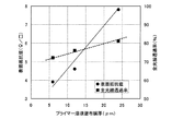
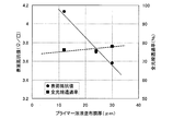
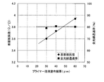
後述の実施例、図1~図3に示すようにいずれも70%以上の良好な光学的透過特性を有し、さらに界面活性剤を含むプライマー溶液の塗布膜厚と表面抵抗値との間に相関性を有し、界面活性剤を含むプライマー溶液の塗布膜厚により導電性が制御されていることが分かる。
前記界面活性剤を含むプライマー上に塗布、乾燥させ、網目状構造物を形成する金属微粒子を含む溶液は、自己組織化現象により網目状構造物を形成するものであれば特に限定されず、このような溶液にはW/O型乳濁液又はW/O型エマルションがある。自己組織化現象により網目状構造物を形成する必要があるため、例えば、分散安定性が悪く、金属微粒子が短時間のうちに沈降するW/O型乳濁液又はW/O型エマルションであれば、塗布される界面活性剤を含むプライマーに関係なく自己組織化現象が良好に生じないため好ましくない。又は、塗布直後にW/O型乳濁液又はW/O型エマルションのチキソトロピー性がなくなり、構造が瞬時に固まってしまうような特性を有するW/O型乳濁液又はW/O型エマルションは好ましくない。金属微粒子を含むW/O型乳濁液又はW/O型エマルションとしては、例えば特許文献1又は特許文献2に記載の金属微粒子を含むW/O型乳濁液又はW/O型のエマルションを用いるのが好ましい。
金属微粒子としては導電性を有する金属又は2種以上の金属の合金を用いることが好ましい。さらには、金、銀、銅、ニッケル、白金、パラジウム又はこれらの合金がより好ましい。
金属微粒子のW/O型乳濁液又はW/O型エマルション中での分散安定性及び塗布、乾燥後の自己組織化現象の促進、さらには低温での焼結性を考慮すると、金属微粒子の平均粒子径は5μm以下が好ましい。より好ましくは1μm以下であり、さらにより好ましくは0.1μm以下である。なお、下限は通常0.001μmである。
各金属微粒子の表面は、金属微粒子の表面酸化の防止又は金属微粒子同士の凝集又は焼結防止のために有機物又は無機物又はその両方が表面に被覆されていても良い。
前記金属微粒子を含むW/O型乳濁液又はW/O型エマルションを前記プライマー上に塗布する場合、同業者が用いる一般的なコーティング法を採用することが出来る。例えばバーコート、ダイコート、ロールコート、スプレーコート、スピンコート、ディップコート、フローコートなどを用いることが出来る。
前記金属微粒子を含むW/O型乳濁液又はW/O型エマルションを塗布、乾燥した後、基材と界面活性剤を含むプライマーの耐薬品性及び耐熱性の許容する程度で化学処理又は加熱処理することで、透明導電性膜積層基材の導電性を向上させることが可能となり、低抵抗な透明導電性膜積層基材を得る場合にはより好ましい。
化学処理としては、アセトン、メタノール、エタノール、酢酸エチル、メチルエチルケトンなどの有機溶剤及び/又は塩酸、酢酸、蟻酸などの無機酸や有機酸に透明導電性膜積層基材を浸漬後、乾燥させる方法が良い。アセトン又はメタノールなどの有機溶剤及び塩酸、蟻酸などに30秒~10分間浸漬するのが好ましい。
加熱処理としては100~200℃、好ましくは100~150℃の温度で30秒~10分間加熱することが好ましい。
上述した基材及び界面活性剤を含むプライマー及び金属微粒子と金属微粒子を含むW/O型乳濁液又はW/O型エマルションを用い、界面活性剤を含むプライマー溶液の塗布膜厚を制御して得られる透明導電性膜積層基材の全光線透過率は70%以上であり、表面抵抗値は1~50Ω/□である。好ましくは全光線透過率は75%以上、表面抵抗値は10Ω/□以下であり、より好ましくは全光線透過率80%以上、表面抵抗値は5Ω/□以下である。全光線透過率が70%未満の場合は、透明性が十分であると言い難く好ましくない。また表面抵抗値が50Ω/□より大きい場合は、高導電性膜とは言い難く好ましくない。
<プライマー層の塗布膜厚の制御>
全自動バーコーター(RKプリントコートインスツルメント社製 K202コーター)を用いて界面活性剤を含むプライマー溶液の塗布厚を制御した。
全自動バーコーター(RKプリントコートインスツルメント社製 K202コーター)を用いて界面活性剤を含むプライマー溶液の塗布厚を制御した。
以下、金属微粒子として銀微粒子を用いた場合について記述するが、銀微粒子以外でも同様の操作により金属微粒子を含むW/O型乳濁液を調製することができる。
<銀微粒子の調製>
硝酸銀40g、ブチルアミン37.9g、メタノール200mLを加え、1時間攪拌しA液を調製した。別にイソアスコルビン酸62.2gを取り、水400mLを加え攪拌して溶解し、続いてメタノール200mLを加えB液を調製した。B液をよく攪拌しA液をB液に1時間20分かけて滴下した。滴下終了後、3時間30分攪拌を継続した。攪拌終了後、30分間静置し固形物を沈降させた。上澄みをデカンテーションにより取り除いた後、新たに水500mLを加え、攪拌、静置、デカンテーションにより上澄み液を取り除いた。この精製操作を3回繰り返した。沈降した固形物を40℃の乾燥機中で乾燥し、水分を除去した。得られた銀微粒子20gと、表面疎水化剤としてDisperbyk-106(ビックケミージャパン社製)等を含む混合物0.2gをメタノール100mLと純水5mLの混合溶液中に混合し、1時間混合した後に、純水100mLを加えて、スラリーをろ過した後、40℃の乾燥機中で乾燥させて、銀微粒子を得た。銀微粒子は電子顕微鏡による観察から一次粒子の平均粒子径が60nmであった。
硝酸銀40g、ブチルアミン37.9g、メタノール200mLを加え、1時間攪拌しA液を調製した。別にイソアスコルビン酸62.2gを取り、水400mLを加え攪拌して溶解し、続いてメタノール200mLを加えB液を調製した。B液をよく攪拌しA液をB液に1時間20分かけて滴下した。滴下終了後、3時間30分攪拌を継続した。攪拌終了後、30分間静置し固形物を沈降させた。上澄みをデカンテーションにより取り除いた後、新たに水500mLを加え、攪拌、静置、デカンテーションにより上澄み液を取り除いた。この精製操作を3回繰り返した。沈降した固形物を40℃の乾燥機中で乾燥し、水分を除去した。得られた銀微粒子20gと、表面疎水化剤としてDisperbyk-106(ビックケミージャパン社製)等を含む混合物0.2gをメタノール100mLと純水5mLの混合溶液中に混合し、1時間混合した後に、純水100mLを加えて、スラリーをろ過した後、40℃の乾燥機中で乾燥させて、銀微粒子を得た。銀微粒子は電子顕微鏡による観察から一次粒子の平均粒子径が60nmであった。
<銀微粒子を含むW/O型乳濁液の調製方法>
特許文献1を参考に銀微粒子を含むW/O型乳濁液の調製を行った。
上述の方法で得られた銀微粒子(平均粒子径60nm)を4g、トルエン等の溶媒を30g、BYK-410(ビックケミージャパン社製)等の結合剤0.2gを混合し、出力180Wの超音波分散機で1.5分間分散化処理を行い、純水15gを添加し、得られた乳濁液を出力180Wの超音波分散機で30秒間分散処理を行い、銀微粒子を含むW/O型乳濁液を調製した。
特許文献1を参考に銀微粒子を含むW/O型乳濁液の調製を行った。
上述の方法で得られた銀微粒子(平均粒子径60nm)を4g、トルエン等の溶媒を30g、BYK-410(ビックケミージャパン社製)等の結合剤0.2gを混合し、出力180Wの超音波分散機で1.5分間分散化処理を行い、純水15gを添加し、得られた乳濁液を出力180Wの超音波分散機で30秒間分散処理を行い、銀微粒子を含むW/O型乳濁液を調製した。
<透明導電性膜の「光学的透過率」、「導電性」の測定方法>
作成した透明導電性膜積層基材の電気抵抗の測定は、JIS-K-7194に準拠した形で、ロレスタ-GP(株式会社ダイアインスツルメンツ製、型番:MCP-T610)において直列4探針プローブ(ASP)を用いて4端子4探針法で実施した。
作成した透明導電性膜積層基材の電気抵抗の測定は、JIS-K-7194に準拠した形で、ロレスタ-GP(株式会社ダイアインスツルメンツ製、型番:MCP-T610)において直列4探針プローブ(ASP)を用いて4端子4探針法で実施した。
光学的透過率は全光線透過率として評価した。前記透明導電性膜積層基材をヘイズメーター(型番:NDH-2000、日本電飾工業株式会社製)を用いてJIS K-7105に準拠して測定した。
<実施例1>
プライマーとしてポリオキシエチレン-β-ナフチルエーテル0.5%(青木油脂工業社製)、BYK-348(ビックケミージャパン社製)0.25%を溶解させたアセトン溶液を調製した。次に市販のPETフィルム上へバーコーターを用いて塗布膜厚(6,12,24μm)を変えながら前記プライマーを含むアセトン溶液(プライマー溶液)を塗布し、大気中で自然乾燥させた。上述した銀微粒子を含むW/O型乳濁液を、バーコーターを用い塗布膜厚30μmで前記プライマーがコーティングされたPETフィルム上に塗布し、乾燥させることで主に銀微粒子で構成される網目状構造を有した透明導電性膜積層基材を得た。続いて、前記透明導電性膜積層基材を150℃で2分間加熱した後、アセトン及び1N塩酸にそれぞれ浸漬し、さらに150℃で2分間加熱乾燥させることで良好な光学的透過特性および導電性を有する透明導電性膜積層基材を得た。
プライマーとしてポリオキシエチレン-β-ナフチルエーテル0.5%(青木油脂工業社製)、BYK-348(ビックケミージャパン社製)0.25%を溶解させたアセトン溶液を調製した。次に市販のPETフィルム上へバーコーターを用いて塗布膜厚(6,12,24μm)を変えながら前記プライマーを含むアセトン溶液(プライマー溶液)を塗布し、大気中で自然乾燥させた。上述した銀微粒子を含むW/O型乳濁液を、バーコーターを用い塗布膜厚30μmで前記プライマーがコーティングされたPETフィルム上に塗布し、乾燥させることで主に銀微粒子で構成される網目状構造を有した透明導電性膜積層基材を得た。続いて、前記透明導電性膜積層基材を150℃で2分間加熱した後、アセトン及び1N塩酸にそれぞれ浸漬し、さらに150℃で2分間加熱乾燥させることで良好な光学的透過特性および導電性を有する透明導電性膜積層基材を得た。
得られた透明導電性膜積層基材の表面抵抗値及び全光線透過率を測定したところ、プライマーの塗布膜厚に対して、いずれも70%以上の良好な光学的透過特性を保持した上に、表面抵抗値をプライマーの塗布膜厚により制御出来ていることが分かった(図1)。
<実施例2>
プライマーとしてポリオキシエチレンオレイルエーテル0.4%(青木油脂工業社製)、BYK-348(ビックケミージャパン社製)0.2%を溶解させたアセトン溶液を調製した。次に市販のPETフィルム上へバーコーターを用いて塗布膜厚(12,24,30μm)を変えながら前記プライマーを含むアセトン溶液を塗布し、大気中で自然乾燥させた。上述した銀微粒子を含むW/O型乳濁液を、バーコーターを用い塗布膜厚30μmで前記プライマーがコーティングされたPETフィルム上に塗布し、乾燥させることで主に銀微粒子で構成される網目状構造を有した透明導電性膜積層基材を得た。続いて、前記透明導電性膜積層基材を150℃で2分間加熱した後、アセトン及び1N塩酸にそれぞれ浸漬し、さらに150℃で2分間加熱乾燥させることで良好な光学的透過特性および導電性を有する透明導電性膜積層基材を得た。
プライマーとしてポリオキシエチレンオレイルエーテル0.4%(青木油脂工業社製)、BYK-348(ビックケミージャパン社製)0.2%を溶解させたアセトン溶液を調製した。次に市販のPETフィルム上へバーコーターを用いて塗布膜厚(12,24,30μm)を変えながら前記プライマーを含むアセトン溶液を塗布し、大気中で自然乾燥させた。上述した銀微粒子を含むW/O型乳濁液を、バーコーターを用い塗布膜厚30μmで前記プライマーがコーティングされたPETフィルム上に塗布し、乾燥させることで主に銀微粒子で構成される網目状構造を有した透明導電性膜積層基材を得た。続いて、前記透明導電性膜積層基材を150℃で2分間加熱した後、アセトン及び1N塩酸にそれぞれ浸漬し、さらに150℃で2分間加熱乾燥させることで良好な光学的透過特性および導電性を有する透明導電性膜積層基材を得た。
得られた透明導電性膜積層基材の表面抵抗値及び全光線透過率を測定したところ、プライマーの塗布膜厚に対して、いずれも70%以上の良好な光学的透過特性を保持した上に、表面抵抗値をプライマーの塗布膜厚により制御出来ていることが分かった(図2)。
<実施例3>
プライマーとしてポリオキシエチレントリスチレン化フェニルエーテル0.3%(青木油脂工業社製)、BYK-348(ビックケミージャパン社製)0.1%を溶解させたアセトン溶液を調製した。次に市販のPETフィルム上へバーコーターを用いて塗布膜厚(30,40,60μm)を変えながら前記プライマーを含むアセトン溶液を塗布し、大気中で自然乾燥させた。上述した銀微粒子を含むW/O型乳濁液を、バーコーターを用い塗布膜厚30μmで前記プライマーがコーティングされたPETフィルム上に塗布し、乾燥させることで主に銀微粒子で構成される網目状構造を有した透明導電性膜積層基材を得た。続いて、前記透明導電性膜積層基材を150℃で2分間加熱した後、アセトン及び1N塩酸にそれぞれ浸漬し、さらに150℃で2分間加熱乾燥させることで良好な光学的透過特性および導電性を有する透明導電性膜積層基材を得た。
プライマーとしてポリオキシエチレントリスチレン化フェニルエーテル0.3%(青木油脂工業社製)、BYK-348(ビックケミージャパン社製)0.1%を溶解させたアセトン溶液を調製した。次に市販のPETフィルム上へバーコーターを用いて塗布膜厚(30,40,60μm)を変えながら前記プライマーを含むアセトン溶液を塗布し、大気中で自然乾燥させた。上述した銀微粒子を含むW/O型乳濁液を、バーコーターを用い塗布膜厚30μmで前記プライマーがコーティングされたPETフィルム上に塗布し、乾燥させることで主に銀微粒子で構成される網目状構造を有した透明導電性膜積層基材を得た。続いて、前記透明導電性膜積層基材を150℃で2分間加熱した後、アセトン及び1N塩酸にそれぞれ浸漬し、さらに150℃で2分間加熱乾燥させることで良好な光学的透過特性および導電性を有する透明導電性膜積層基材を得た。
得られた透明導電性膜積層基材の表面抵抗値及び全光線透過率を測定したところ、プライマーの塗布膜厚に対して、いずれも70%以上の良好な光学的透過特性を保持した上に、表面抵抗値をプライマーの塗布膜厚により制御出来ていることが分かった(図3)。
<比較例1>
プライマーとしてポリオキシエチレン-β-ナフチルエーテル1.2%(青木油脂工業社製)、ポリエーテル変性ポリジメチルシロキサンの代わりにフッ素変性ポリマーであるBYK-340(ビックケミージャパン社製)2.0%を溶解させたアセトン溶液を調製した。次に市販のPETフィルム上へバーコーターを用いて塗布膜厚(6,12,24μm)を変えながら前記プライマーを含むアセトン溶液を塗布し、大気中で自然乾燥させた。上述した銀微粒子を含むW/O型乳濁液を、バーコーターを用い塗布膜厚30μmで前記プライマーがコーティングされたPETフィルム上に塗布し、乾燥させることで主に銀微粒子で構成される網目状構造を有した透明導電性膜積層基材を得た。続いて、前記透明導電性膜積層基材を150℃で2分間加熱した後、アセトン及び1N塩酸にそれぞれ浸漬し、さらに150℃で2分間加熱乾燥させ透明導電性膜積層基材を得た。
プライマーとしてポリオキシエチレン-β-ナフチルエーテル1.2%(青木油脂工業社製)、ポリエーテル変性ポリジメチルシロキサンの代わりにフッ素変性ポリマーであるBYK-340(ビックケミージャパン社製)2.0%を溶解させたアセトン溶液を調製した。次に市販のPETフィルム上へバーコーターを用いて塗布膜厚(6,12,24μm)を変えながら前記プライマーを含むアセトン溶液を塗布し、大気中で自然乾燥させた。上述した銀微粒子を含むW/O型乳濁液を、バーコーターを用い塗布膜厚30μmで前記プライマーがコーティングされたPETフィルム上に塗布し、乾燥させることで主に銀微粒子で構成される網目状構造を有した透明導電性膜積層基材を得た。続いて、前記透明導電性膜積層基材を150℃で2分間加熱した後、アセトン及び1N塩酸にそれぞれ浸漬し、さらに150℃で2分間加熱乾燥させ透明導電性膜積層基材を得た。
得られた透明導電性膜積層基材の表面抵抗値及び全光線透過率を測定したところ、プライマーの塗布膜厚に対して表面抵抗値が制御できておらず、さらに全光線透過率はいずれも70%を下回った低いものであった(図4)。
<参考例1>
プライマーとしてポリオキシエチレン-β-ナフチルエーテル1.2%(青木油脂工業社製)、ポリエーテル変性ポリジメチルシロキサンの代わりにエチレン酢酸ビニル共重合物ワックスディスパージョンであるCERAFAK-106(ビックケミージャパン社製)2.0%を溶解させたアセトン溶液を調製した。次に市販のPETフィルム上へバーコーターを用いて塗布膜厚(12,24,30μm)を変えながら前記プライマーを含むアセトン溶液を塗布し、大気中で自然乾燥させた。上述した銀微粒子を含むW/O型乳濁液を、バーコーターを用い塗布膜厚30μmで前記プライマーがコーティングされたPETフィルム上に塗布し、乾燥させることで主に銀微粒子で構成される網目状構造を有した導電性膜積層基材を得た。続いて、前記導電性膜積層基材を150℃で2分間加熱した後、アセトン及び1N塩酸にそれぞれ浸漬し、さらに150℃で2分間加熱乾燥させ導電性膜積層基材を得た。
プライマーとしてポリオキシエチレン-β-ナフチルエーテル1.2%(青木油脂工業社製)、ポリエーテル変性ポリジメチルシロキサンの代わりにエチレン酢酸ビニル共重合物ワックスディスパージョンであるCERAFAK-106(ビックケミージャパン社製)2.0%を溶解させたアセトン溶液を調製した。次に市販のPETフィルム上へバーコーターを用いて塗布膜厚(12,24,30μm)を変えながら前記プライマーを含むアセトン溶液を塗布し、大気中で自然乾燥させた。上述した銀微粒子を含むW/O型乳濁液を、バーコーターを用い塗布膜厚30μmで前記プライマーがコーティングされたPETフィルム上に塗布し、乾燥させることで主に銀微粒子で構成される網目状構造を有した導電性膜積層基材を得た。続いて、前記導電性膜積層基材を150℃で2分間加熱した後、アセトン及び1N塩酸にそれぞれ浸漬し、さらに150℃で2分間加熱乾燥させ導電性膜積層基材を得た。
得られた導電性基板の表面抵抗値及び全光線透過率を測定したところ、プライマーの塗布膜厚に対して表面抵抗値に相関性が見られ良く制御できているが、全光線透過率はいずれも70%を下回った低いものであった(図5)。
<比較例2>
プライマーとしてポリオキシエチレン-β-ナフチルエーテル1.0%(青木油脂工業社製)、BYK-348(ビックケミージャパン社製)0.5%を溶解させたアセトン溶液を調製した。次に市販のPETフィルム上へバーコーターを用いて塗布膜厚100μmになるように前記プライマーを含むアセトン溶液を塗布し、大気中で自然乾燥させた。上述した銀微粒子を含むW/O型乳濁液を、バーコーターを用い塗布膜厚30μmで前記プライマーがコーティングされたPETフィルム上に塗布し、乾燥させたが、網目状構造物が得られず、全光線透過率は90.05%であったが、表面抵抗値は測定できないほど高抵抗であった。
プライマーとしてポリオキシエチレン-β-ナフチルエーテル1.0%(青木油脂工業社製)、BYK-348(ビックケミージャパン社製)0.5%を溶解させたアセトン溶液を調製した。次に市販のPETフィルム上へバーコーターを用いて塗布膜厚100μmになるように前記プライマーを含むアセトン溶液を塗布し、大気中で自然乾燥させた。上述した銀微粒子を含むW/O型乳濁液を、バーコーターを用い塗布膜厚30μmで前記プライマーがコーティングされたPETフィルム上に塗布し、乾燥させたが、網目状構造物が得られず、全光線透過率は90.05%であったが、表面抵抗値は測定できないほど高抵抗であった。
実施例1~3、参考例1及び比較例1~2の結果を表1に示した。

Claims (11)
- プライマーと、当該プライマー上に形成された金属微粒子を主成分として構成される網目状構造物とからなる透明導電性膜が基材上に積層されている透明導電性膜積層基材であって、当該プライマーが、透明導電性膜の表面抵抗を制御可能であることを特徴とする透明導電性膜積層基材。
- プライマーと、当該プライマー上に形成された金属微粒子を主成分として構成される網目状構造物とからなる透明導電性膜が基材上に積層されている透明導電性膜積層基材であって、当該プライマーが金属微粒子を主成分として形成される網目状構造物の光学的特性および導電性を制御可能であることを特徴とする透明導電性膜積層基材。
- 前記透明導電性膜の全光線透過率が70%以上であり、表面抵抗値が50Ω/□以下である請求項1又は2に記載の透明導電性膜積層基材。
- 前記プライマーが酸化エチレン誘導体及びポリエーテル変性ポリジメチルシロキサンを含む請求項1~3の何れかに記載の透明導電性膜積層基材。
- 前記金属微粒子が金、銀、銅、ニッケル、白金、パラジウム又は前記金属を2種以上含む合金である請求項1~4の何れかに記載の透明導電性膜積層基材。
- 基材表面に界面活性剤を含有するプライマー溶液を1μm以上100μm未満の膜厚で塗布、乾燥させた後、基材表面に形成されたプライマー上に網目状構造物を形成可能な金属微粒子分散溶液を塗布、乾燥させ、透明導電性膜を形成させることを特徴とする請求項1~3の何れかに記載の透明導電性膜積層基材の製造方法。
- 界面活性剤が酸化エチレン誘導体及びポリエーテル変性ポリジメチルシロキサンから成る請求項6に記載の透明導電性膜積層基材の製造方法。
- 前記金属微粒子が金、銀、銅、ニッケル、白金、パラジウム又は前記金属を2種以上含む合金である請求項6又は7に記載の透明導電性膜積層基材の製造方法。
- さらに前記透明導電性膜に対して化学的処理及び/又は加熱処理を施す請求項6~8の何れかに記載の透明導電性膜積層基材の製造方法。
- 前記基材表面に塗布するプライマー溶液の膜厚を制御し、前記透明導電性膜の表面抵抗値を所定の値に制御する請求項6~9の何れかに記載の透明導電性膜積層基材の製造方法。
- 前記基材表面に塗布するプライマー溶液の膜厚を制御し、前記網目状構造物の構造を制御する請求項6~9の何れかに記載の透明導電性膜積層基材の製造方法。
Priority Applications (1)
| Application Number | Priority Date | Filing Date | Title |
|---|---|---|---|
| JP2010549458A JPWO2010090158A1 (ja) | 2009-02-03 | 2010-02-01 | 透明導電性膜積層基材及びその製造方法 |
Applications Claiming Priority (2)
| Application Number | Priority Date | Filing Date | Title |
|---|---|---|---|
| JP2009023144 | 2009-02-03 | ||
| JP2009-023144 | 2009-02-03 |
Publications (1)
| Publication Number | Publication Date |
|---|---|
| WO2010090158A1 true WO2010090158A1 (ja) | 2010-08-12 |
Family
ID=42542052
Family Applications (1)
| Application Number | Title | Priority Date | Filing Date |
|---|---|---|---|
| PCT/JP2010/051361 Ceased WO2010090158A1 (ja) | 2009-02-03 | 2010-02-01 | 透明導電性膜積層基材及びその製造方法 |
Country Status (3)
| Country | Link |
|---|---|
| JP (1) | JPWO2010090158A1 (ja) |
| TW (1) | TW201042668A (ja) |
| WO (1) | WO2010090158A1 (ja) |
Cited By (3)
| Publication number | Priority date | Publication date | Assignee | Title |
|---|---|---|---|---|
| JP2015532669A (ja) * | 2012-08-16 | 2015-11-12 | シーマ ナノテック イスラエル リミテッド | 透明な導電性コーティングを調製するためのエマルション |
| JP2019110264A (ja) * | 2017-12-20 | 2019-07-04 | 日立化成株式会社 | 構造体及びその製造方法 |
| CN112251137A (zh) * | 2020-10-14 | 2021-01-22 | 中国工程物理研究院激光聚变研究中心 | 晶体涂膜元件及其制备方法、晶体膜系 |
Families Citing this family (1)
| Publication number | Priority date | Publication date | Assignee | Title |
|---|---|---|---|---|
| CN112940308B (zh) * | 2021-01-14 | 2023-01-03 | 西安交通大学 | 一种透明/不透明状态可开关的pdms超疏水柔性膜制备方法 |
Citations (3)
| Publication number | Priority date | Publication date | Assignee | Title |
|---|---|---|---|---|
| JP2004228057A (ja) * | 2002-11-25 | 2004-08-12 | Fuji Photo Film Co Ltd | 網目状導電体及びその製造方法並びに用途 |
| JP2008041445A (ja) * | 2006-08-07 | 2008-02-21 | Asahi Glass Co Ltd | 透明導電膜の製造方法および透明導電膜 |
| JP2010093239A (ja) * | 2008-09-09 | 2010-04-22 | Toray Ind Inc | 網目状金属微粒子積層基板及び透明導電性基板の製造方法 |
-
2010
- 2010-02-01 WO PCT/JP2010/051361 patent/WO2010090158A1/ja not_active Ceased
- 2010-02-01 JP JP2010549458A patent/JPWO2010090158A1/ja not_active Withdrawn
- 2010-02-03 TW TW99103178A patent/TW201042668A/zh unknown
Patent Citations (3)
| Publication number | Priority date | Publication date | Assignee | Title |
|---|---|---|---|---|
| JP2004228057A (ja) * | 2002-11-25 | 2004-08-12 | Fuji Photo Film Co Ltd | 網目状導電体及びその製造方法並びに用途 |
| JP2008041445A (ja) * | 2006-08-07 | 2008-02-21 | Asahi Glass Co Ltd | 透明導電膜の製造方法および透明導電膜 |
| JP2010093239A (ja) * | 2008-09-09 | 2010-04-22 | Toray Ind Inc | 網目状金属微粒子積層基板及び透明導電性基板の製造方法 |
Cited By (5)
| Publication number | Priority date | Publication date | Assignee | Title |
|---|---|---|---|---|
| JP2015532669A (ja) * | 2012-08-16 | 2015-11-12 | シーマ ナノテック イスラエル リミテッド | 透明な導電性コーティングを調製するためのエマルション |
| JP2019110264A (ja) * | 2017-12-20 | 2019-07-04 | 日立化成株式会社 | 構造体及びその製造方法 |
| JP7095274B2 (ja) | 2017-12-20 | 2022-07-05 | 昭和電工マテリアルズ株式会社 | 構造体及びその製造方法 |
| CN112251137A (zh) * | 2020-10-14 | 2021-01-22 | 中国工程物理研究院激光聚变研究中心 | 晶体涂膜元件及其制备方法、晶体膜系 |
| CN112251137B (zh) * | 2020-10-14 | 2022-05-10 | 中国工程物理研究院激光聚变研究中心 | 晶体涂膜元件及其制备方法、晶体膜系 |
Also Published As
| Publication number | Publication date |
|---|---|
| TW201042668A (en) | 2010-12-01 |
| JPWO2010090158A1 (ja) | 2012-08-09 |
Similar Documents
| Publication | Publication Date | Title |
|---|---|---|
| KR101570398B1 (ko) | 투명 도전성 잉크 및 투명 도전 패턴형성방법 | |
| JP5632852B2 (ja) | 低温焼結性銀ナノ粒子組成物および該組成物を用いて形成された電子物品 | |
| JP4636496B2 (ja) | 導電性及び透明性を有するナノ被覆物及びナノインクの製造方法、並びにこの製造方法により製造されるナノ粉末被覆物及びインク | |
| KR102032108B1 (ko) | 금속성 나노섬유 잉크, 실질적으로 투명한 전도체, 및 제조 방법 | |
| CA2888035C (en) | Stretchable conductive film based on silver nanoparticles | |
| JP5227570B2 (ja) | 透明導電性部材の製造方法 | |
| CN102575117A (zh) | 用于提高由金属纳米结构制成的透明导体雾度的金属纳米结构的纯化 | |
| KR102169003B1 (ko) | 전도성 잉크 조성물, 이를 포함하는 투명 전도성 필름 및 투명 전도성 필름의 제조방법 | |
| CN1671805A (zh) | 烧结温度低的导电纳米油墨及其制备方法 | |
| WO2015025792A1 (ja) | 透明電極及びその製造方法 | |
| US10362685B2 (en) | Protective coating for printed conductive pattern on patterned nanowire transparent conductors | |
| JP2004196923A (ja) | 金属ナノワイヤー含有組成物および電磁波遮蔽フィルター | |
| WO2010090158A1 (ja) | 透明導電性膜積層基材及びその製造方法 | |
| JP5326647B2 (ja) | 太陽電池の電極形成用組成物の製造方法 | |
| JP5446097B2 (ja) | 導電性基板及びその製造方法 | |
| KR101319259B1 (ko) | 투명 전극 형성용 은 나노와이어 수용성 잉크 조성물 및 이를 이용한 투명 전극 형성방법 | |
| CN109074919A (zh) | 透明导电图案的形成方法 | |
| JP6136622B2 (ja) | 透明導電膜用水系塗工液及びこれを用いた透明導電膜 | |
| JP4635888B2 (ja) | 導電性ペーストおよび導電性回路の製造方法 | |
| TW201044463A (en) | Transparent conductive film encapsulating mesh-like structure formed from metal microparticles, substrate on which transparent conductive film is laminated, and method for producing the same | |
| JP2015514265A (ja) | 導電性パターン形成用基材およびこれを用いて形成された導電性パターン | |
| JP2012031478A (ja) | 銀微粒子とその製造方法、並びに該銀微粒子を含有する導電性ペースト、導電性膜及び電子デバイス | |
| Sakurai et al. | Filtration-induced production of conductive/robust Cu films on cellulose paper by low-temperature sintering in air | |
| JP2015504375A (ja) | 基材上の整合したネットワーク | |
| CN103680758B (zh) | 制造银迷你线薄膜的方法 |
Legal Events
| Date | Code | Title | Description |
|---|---|---|---|
| 121 | Ep: the epo has been informed by wipo that ep was designated in this application |
Ref document number: 10738490 Country of ref document: EP Kind code of ref document: A1 |
|
| ENP | Entry into the national phase |
Ref document number: 2010549458 Country of ref document: JP Kind code of ref document: A |
|
| NENP | Non-entry into the national phase |
Ref country code: DE |
|
| 122 | Ep: pct application non-entry in european phase |
Ref document number: 10738490 Country of ref document: EP Kind code of ref document: A1 |