WO2010073457A1 - 粉末、その製造方法、及びその粉末を含む樹脂組成物 - Google Patents
粉末、その製造方法、及びその粉末を含む樹脂組成物 Download PDFInfo
- Publication number
- WO2010073457A1 WO2010073457A1 PCT/JP2009/005730 JP2009005730W WO2010073457A1 WO 2010073457 A1 WO2010073457 A1 WO 2010073457A1 JP 2009005730 W JP2009005730 W JP 2009005730W WO 2010073457 A1 WO2010073457 A1 WO 2010073457A1
- Authority
- WO
- WIPO (PCT)
- Prior art keywords
- powder
- particles
- magnetized
- particle diameter
- spherical
- Prior art date
- Legal status (The legal status is an assumption and is not a legal conclusion. Google has not performed a legal analysis and makes no representation as to the accuracy of the status listed.)
- Ceased
Links
Classifications
-
- C—CHEMISTRY; METALLURGY
- C01—INORGANIC CHEMISTRY
- C01B—NON-METALLIC ELEMENTS; COMPOUNDS THEREOF; METALLOIDS OR COMPOUNDS THEREOF NOT COVERED BY SUBCLASS C01C
- C01B33/00—Silicon; Compounds thereof
- C01B33/113—Silicon oxides; Hydrates thereof
- C01B33/12—Silica; Hydrates thereof, e.g. lepidoic silicic acid
- C01B33/18—Preparation of finely divided silica neither in sol nor in gel form; After-treatment thereof
-
- H—ELECTRICITY
- H10—SEMICONDUCTOR DEVICES; ELECTRIC SOLID-STATE DEVICES NOT OTHERWISE PROVIDED FOR
- H10W—GENERIC PACKAGES, INTERCONNECTIONS, CONNECTORS OR OTHER CONSTRUCTIONAL DETAILS OF DEVICES COVERED BY CLASS H10
- H10W74/00—Encapsulations, e.g. protective coatings
- H10W74/40—Encapsulations, e.g. protective coatings characterised by their materials
- H10W74/481—Encapsulations, e.g. protective coatings characterised by their materials comprising semiconductor materials
-
- B—PERFORMING OPERATIONS; TRANSPORTING
- B01—PHYSICAL OR CHEMICAL PROCESSES OR APPARATUS IN GENERAL
- B01J—CHEMICAL OR PHYSICAL PROCESSES, e.g. CATALYSIS OR COLLOID CHEMISTRY; THEIR RELEVANT APPARATUS
- B01J2/00—Processes or devices for granulating materials, e.g. fertilisers in general; Rendering particulate materials free flowing in general, e.g. making them hydrophobic
- B01J2/16—Processes or devices for granulating materials, e.g. fertilisers in general; Rendering particulate materials free flowing in general, e.g. making them hydrophobic by suspending the powder material in a gas, e.g. in fluidised beds or as a falling curtain
-
- C—CHEMISTRY; METALLURGY
- C01—INORGANIC CHEMISTRY
- C01F—COMPOUNDS OF THE METALS BERYLLIUM, MAGNESIUM, ALUMINIUM, CALCIUM, STRONTIUM, BARIUM, RADIUM, THORIUM, OR OF THE RARE-EARTH METALS
- C01F7/00—Compounds of aluminium
- C01F7/02—Aluminium oxide; Aluminium hydroxide; Aluminates
-
- C—CHEMISTRY; METALLURGY
- C01—INORGANIC CHEMISTRY
- C01F—COMPOUNDS OF THE METALS BERYLLIUM, MAGNESIUM, ALUMINIUM, CALCIUM, STRONTIUM, BARIUM, RADIUM, THORIUM, OR OF THE RARE-EARTH METALS
- C01F7/00—Compounds of aluminium
- C01F7/02—Aluminium oxide; Aluminium hydroxide; Aluminates
- C01F7/021—After-treatment of oxides or hydroxides
- C01F7/027—Treatment involving fusion or vaporisation
-
- C—CHEMISTRY; METALLURGY
- C08—ORGANIC MACROMOLECULAR COMPOUNDS; THEIR PREPARATION OR CHEMICAL WORKING-UP; COMPOSITIONS BASED THEREON
- C08K—Use of inorganic or non-macromolecular organic substances as compounding ingredients
- C08K3/00—Use of inorganic substances as compounding ingredients
- C08K3/18—Oxygen-containing compounds, e.g. metal carbonyls
- C08K3/20—Oxides; Hydroxides
- C08K3/22—Oxides; Hydroxides of metals
-
- C—CHEMISTRY; METALLURGY
- C08—ORGANIC MACROMOLECULAR COMPOUNDS; THEIR PREPARATION OR CHEMICAL WORKING-UP; COMPOSITIONS BASED THEREON
- C08L—COMPOSITIONS OF MACROMOLECULAR COMPOUNDS
- C08L63/00—Compositions of epoxy resins; Compositions of derivatives of epoxy resins
-
- H—ELECTRICITY
- H10—SEMICONDUCTOR DEVICES; ELECTRIC SOLID-STATE DEVICES NOT OTHERWISE PROVIDED FOR
- H10W—GENERIC PACKAGES, INTERCONNECTIONS, CONNECTORS OR OTHER CONSTRUCTIONAL DETAILS OF DEVICES COVERED BY CLASS H10
- H10W74/00—Encapsulations, e.g. protective coatings
- H10W74/40—Encapsulations, e.g. protective coatings characterised by their materials
- H10W74/47—Encapsulations, e.g. protective coatings characterised by their materials comprising organic materials, e.g. plastics or resins
-
- C—CHEMISTRY; METALLURGY
- C01—INORGANIC CHEMISTRY
- C01P—INDEXING SCHEME RELATING TO STRUCTURAL AND PHYSICAL ASPECTS OF SOLID INORGANIC COMPOUNDS
- C01P2002/00—Crystal-structural characteristics
- C01P2002/80—Crystal-structural characteristics defined by measured data other than those specified in group C01P2002/70
- C01P2002/85—Crystal-structural characteristics defined by measured data other than those specified in group C01P2002/70 by XPS, EDX or EDAX data
-
- C—CHEMISTRY; METALLURGY
- C01—INORGANIC CHEMISTRY
- C01P—INDEXING SCHEME RELATING TO STRUCTURAL AND PHYSICAL ASPECTS OF SOLID INORGANIC COMPOUNDS
- C01P2004/00—Particle morphology
- C01P2004/30—Particle morphology extending in three dimensions
- C01P2004/32—Spheres
-
- C—CHEMISTRY; METALLURGY
- C01—INORGANIC CHEMISTRY
- C01P—INDEXING SCHEME RELATING TO STRUCTURAL AND PHYSICAL ASPECTS OF SOLID INORGANIC COMPOUNDS
- C01P2004/00—Particle morphology
- C01P2004/60—Particles characterised by their size
- C01P2004/61—Micrometer sized, i.e. from 1-100 micrometer
-
- C—CHEMISTRY; METALLURGY
- C01—INORGANIC CHEMISTRY
- C01P—INDEXING SCHEME RELATING TO STRUCTURAL AND PHYSICAL ASPECTS OF SOLID INORGANIC COMPOUNDS
- C01P2006/00—Physical properties of inorganic compounds
- C01P2006/42—Magnetic properties
-
- Y—GENERAL TAGGING OF NEW TECHNOLOGICAL DEVELOPMENTS; GENERAL TAGGING OF CROSS-SECTIONAL TECHNOLOGIES SPANNING OVER SEVERAL SECTIONS OF THE IPC; TECHNICAL SUBJECTS COVERED BY FORMER USPC CROSS-REFERENCE ART COLLECTIONS [XRACs] AND DIGESTS
- Y10—TECHNICAL SUBJECTS COVERED BY FORMER USPC
- Y10T—TECHNICAL SUBJECTS COVERED BY FORMER US CLASSIFICATION
- Y10T428/00—Stock material or miscellaneous articles
- Y10T428/29—Coated or structually defined flake, particle, cell, strand, strand portion, rod, filament, macroscopic fiber or mass thereof
- Y10T428/2982—Particulate matter [e.g., sphere, flake, etc.]
Definitions
- the present invention relates to a powder composed of spherical siliceous powder and / or spherical alumina powder, a production method thereof, and a resin composition containing the powder.
- a semiconductor encapsulant for packaging (sealing) a semiconductor is a siliceous powder for the purpose of lowering the coefficient of thermal expansion, increasing the thermal conductivity, improving flame retardancy, and improving moisture resistance.
- fillers such as alumina powder and the like are filled with fine metal particles as foreign matters in the manufacturing process. This is because part of the manufacturing equipment for fillers such as siliceous powder and alumina powder is generally made of metal such as iron or stainless steel, and the surface is used for pulverizing the powder or air flow. This is because it is scraped by powder when it is transported, classified, sieved, blended, etc.
- Patent Document 1 As a technique for removing or detoxifying (non-conductive) metallic particles in siliceous powder and alumina powder, spherical silica powder containing metallic particles is placed in an aqueous sulfuric acid solution, and the metallic powder is dissolved. A removal method is disclosed (Patent Document 1). However, in this method, it is necessary to wash, heat dry and crush the spherical silica powder after the acid treatment, which is not only costly, but also in the heat drying step and the crushing step for pulverization, There is a problem that there is a large risk that the powdered powder will be mixed again.
- the object of the present invention is to use a spherical siliceous powder and / or alumina that is suitable for preparing a semiconductor encapsulant with a small contamination rate of conductive foreign materials, which is used for encapsulating miniaturized and densified semiconductors. It is providing the powder which consists of powder, its manufacturing method, and a resin composition.
- the number ratio of the magnetized colored particles having a particle diameter of 45 ⁇ m or more is the same as that of the magnetized colored particles having a particle diameter of 45 ⁇ m or more and the particle diameter of 45 ⁇ m.
- a 10,000 gauss bar magnet covered with a rubber cover having a thickness of 20 ⁇ m is immersed in the slurry to capture the magnetized particles, and sieved with a polyester filter having an opening of 45 ⁇ m.
- the number of particles remaining on the filter is regarded as “the total number of magnetized colored particles having a particle size of 45 ⁇ m or more and non-magnetized particles having a particle size of 45 ⁇ m”.
- the colored particles are regarded as “magnetically colored particles having a particle diameter of 45 ⁇ m or more”, and the number thereof is counted. (Number of magnetized colored particles having a particle diameter of 45 ⁇ m or more) ⁇ 100 / (total number of magnetized colored particles having a particle diameter of 45 ⁇ m or more and magnetized non-colored particles having a particle diameter of 45 ⁇ m or more), The number ratio of the magnetized colored particles having a particle diameter of 45 ⁇ m or more present in the magnetized particles having a particle diameter of 45 ⁇ m or more is calculated.
- the analysis conditions for EDS are an acceleration voltage of 15 kV, an irradiation current of 10 nA, a magnification of 2000 times, an integration time of 100 msec per pixel, a pixel size of 0.2 ⁇ m ⁇ , and a pixel count of 256 ⁇ 256 pixels.
- the number of magnetized colored particles having a particle diameter of 45 ⁇ m or more is 5 or less per 50 g of powder, and (ii) the magnetized colored particles having a particle diameter of 45 ⁇ m or more;
- the total number of magnetized non-colored particles having a particle diameter of 45 ⁇ m or more is 50 or less per 50 g of powder, and
- the ratio of the number of particles oxidized to the center is 60% or more, particularly 70% or more.
- the average sphericity of the powder is preferably 0.75 or more and the average particle size is 3 to 50 ⁇ m.
- the present invention includes a step of melting a siliceous powder raw material and / or an alumina powder raw material with a flame formed in a furnace, spheroidizing the material, and then transporting it outside the furnace to collect the spherical powder.
- oxygen gas and / or water vapor of 0.3 to 0.6 m 3 per 1 kg of the raw material powder is added to any at least one portion of the furnace where the ambient temperature is 1600 to 1800 ° C.
- the powder composed of the spherical siliceous powder and / or the spherical alumina powder is preferably any of the powders of the present invention described above.
- the present invention also provides a resin composition containing the powder of the present invention.
- spherical siliceous powder and / or alumina powder suitable for preparing a semiconductor encapsulant with a small contamination rate of conductive foreign substances used for encapsulating miniaturized and densified semiconductors.
- the powder which consists of, the manufacturing method, and the resin composition are provided.
- the powder of the present invention comprises a spherical siliceous powder and / or a spherical alumina powder.
- the semiconductor sealing material using siliceous powder has an advantage that the coefficient of thermal expansion is lower than that using an oxide powder other than siliceous powder.
- the semiconductor sealing material using alumina powder has the advantage that the thermal conductivity is higher than that using oxide powder other than alumina powder.
- the powder composed of siliceous powder and / or alumina powder may be a single powder or a mixed powder of both.
- the average sphericity of the powder of the present invention is preferably 0.75 or more, particularly preferably 0.80 or more, more preferably 0.90 or more. Such average sphericity reduces the viscosity of the semiconductor sealing material, and can easily reduce the occurrence of problems such as wire flow during sealing.
- the average sphericity is measured as follows. That is, a particle image photographed with a stereomicroscope (trade name “Model SMZ-10” manufactured by Nikon Corporation) is taken into an image analysis device (trade name “MacView” manufactured by Mountec Co., Ltd.), and the projected area (A) of the particles from the photograph. And measure the perimeter (PM).
- the sphericity of the particle is A / B.
- B ⁇ ⁇ (PM / 2 ⁇ ) 2
- the sphericity of 200 arbitrary particles is obtained, and the average value is defined as the average sphericity.
- the average particle size of the powder of the present invention is preferably 3 to 50 ⁇ m. If the average particle diameter is less than 3 ⁇ m, the viscosity of the semiconductor encapsulant increases, and there is a possibility that the semiconductor wire is deformed at the time of encapsulation. On the other hand, if the average particle diameter exceeds 50 ⁇ m, the particles may be too coarse to damage the semiconductor chip, or the coarse particles may collide with the semiconductor wire and the wire may be deformed. A particularly preferred average particle size is 5 to 45 ⁇ m.
- the average particle size is a particle size having a cumulative value of 50% by mass in the cumulative particle size distribution of the powder, and can be measured based on particle size measurement by a laser diffraction scattering method.
- water and powder are mixed using a measuring device of trade name “Cirrus Granurometer Model 920” manufactured by Cirrus, and the powder is dispersed with an ultrasonic homogenizer at an output of 200 W for 1 minute. Measure from The particle diameter channels are 1, 1.5, 2, 3, 4, 6, 8, 12, 16, 24, 32, 48, 64, 96, 128, and 196 ⁇ m.
- the siliceous powder of the present invention preferably has an amorphous ratio (melting ratio) of 98% by mass or more.
- the amorphous ratio is determined by X-ray diffraction analysis using a powder X-ray diffractometer (trade name “Model Mini Flex” manufactured by RIGAKU) in the range of 2 ⁇ of CuK ⁇ rays of 26 ° to 27.5 °. Measured from the peak intensity ratio.
- crystalline silica has a main peak at 26.7 °, but amorphous silica has no peak.
- amorphous silica and crystalline silica are mixed, a peak of 26.7 ° having a height corresponding to the ratio of crystalline silica can be obtained.
- the number ratio of the magnetically colored particles having a particle diameter of 45 ⁇ m or more was the same as that of the magnetically colored particles having a particle diameter of 45 ⁇ m or more and the particle diameter of 45 ⁇ m. It is 20% or less, preferably 15% or less, particularly preferably 10% or less, based on the total number of the above magnetized non-coloring particles.
- the fact that particles that are amber colored in magnetized particles of 45 ⁇ m or more (that is, magnetized colored particles having a particle diameter of 45 ⁇ m or more) is included means that part or all of the magnetized particles are dissolved in a 10% by mass hydrochloric acid aqueous solution.
- the magnetized colored particles having a particle size of 45 ⁇ m or more are stainless steel particles, iron particles, and the like, and typical examples of the magnetized non-colored particles having a particle size of 45 ⁇ m or more are iron oxide particles.
- both the magnetized colored particles and the magnetized non-colored particles are captured by a 10,000 G bar magnet.
- magnetized particles having a particle diameter of 45 ⁇ m or more and the conductivity of the magnetized colored particles having a particle diameter of 45 ⁇ m or more are as follows. Almost all of the magnetized particles mixed in the powder are stainless steel (SUS304, SUS316, SUS430, etc.) particles, iron (Fe) particles, and oxides thereof derived from wear, cutting, peeling, etc. of manufacturing equipment. Particles. In the powder manufacturing process, in some heated stainless steel particles and iron particles, oxide films such as hematite (Fe 2 O 3 ) and magnetite (Fe 3 O 4 ) are formed in order from the outside. Are magnetic particles that are captured by a magnet of at least 10,000 Gauss.
- stainless steel particles and iron particles are soluble in hydrochloric acid and have conductivity, but hematite is an insulator having very little hydrochloric acid solubility and almost no conductivity. Therefore, if the solubility of the magnetized particles in the hydrochloric acid aqueous solution can be determined, the magnitude of the conductivity of the magnetized particles can be determined.
- the magnetized colored particles exhibiting an amber color reaction are stainless steel particles, iron particles
- the magnetized non-colored particles that are determined to have conductivity and do not exhibit a color reaction are determined to be those oxide particles having at least a hematite film and not to have conductivity (very small). be able to.
- the powder of the present invention is configured based on such a novel viewpoint.
- the ratio of the number of magnetized colored particles having a particle diameter of 45 ⁇ m or more exceeds 20% with respect to the total number of magnetized colored particles and magnetized non-colored particles having a particle diameter of 45 ⁇ m or more, semiconductor encapsulation
- the number ratio of the magnetized colored particles having a particle diameter of less than 45 ⁇ m is small, but since the distance between the gold wires in the current state-of-the-art semiconductor is about 50 ⁇ m, these particles straddle the gold wires, and the semiconductor This is unlikely to cause a short circuit failure. Therefore, at the present time, it is important to regulate the number ratio of the magnetized colored particles having a particle diameter of 45 ⁇ m or more.
- the number of magnetized colored particles having a particle diameter of 45 ⁇ m or more is preferably 5 or less per 50 g of powder, particularly preferably 3 or less. This promotes the effects of the present invention.
- the ideal number of magnetized colored particles having a particle diameter of 45 ⁇ m or more is 0, but the amount of powder in the semiconductor encapsulant used per semiconductor is about 1 to 3 g. In particular, the short-circuit failure rate of semiconductors due to powder tends to be extremely small. Therefore, if the number of magnetized colored particles having a particle diameter of 45 ⁇ m or more is 5 or less per 50 g of powder, a sufficient effect can be obtained from the viewpoint of reducing short circuit defects in the semiconductor.
- the total number of magnetized colored particles having a particle size of 45 ⁇ m or more and magnetized non-colored particles having a particle size of 45 ⁇ m or more (that is, the number of magnetized particles having a particle size of 45 ⁇ m or more) per 50 g of powder.
- the effect of the present invention can be further enhanced when the number is 50 or less, particularly 40 or less. That is, the non-magnetic colored particles that do not exhibit conductivity may be reduced in advance because the oxide film such as hematite may be destroyed depending on the handling method and may exhibit conductivity again. .
- the number ratio of “particles oxidized to the center” calculated by performing the above (4) is preferably 60% or more, particularly preferably 70% or more.
- the number ratio of the particles oxidized to the center is less than 60%, the effect of the present invention is not drastically impaired.
- osmium was vapor-deposited with the thickness of about 5 nm with the osmium coater, and electroconductivity was provided. Under this condition, 10 cross-sections of arbitrary non-magnetized particles having a diameter of 45 ⁇ m or more were photographed. The number of particles was counted by enlarging with a microscope.
- the number of magnetized colored particles having a particle diameter of 45 ⁇ m or more and the method of increasing / decreasing the number of magnetized non-colored particles having a particle diameter of 45 ⁇ m or more will be described later.
- oxygen gas and What is necessary is just to increase supply_amount
- powder raw material and / or spherical powder and stainless steel and / or iron are used. And the relative speed may be 5 m / s or less.
- the average particle diameter of the powder can be increased or decreased by adjusting the average particle diameter of the powder raw material, and the average sphericity increases as the amount of powder raw material supplied to the flame is reduced.
- a burner that can disperse the powder raw material strongly and inject it into the flame is used in order to increase the average sphericity and prevent the particles from aggregating and melting.
- the strong dispersion of the powder raw material there are particles that go out of the flame without undergoing sufficient heat history in the flame, and there are many magnetized particles that are not oxidized.
- the magnetized particles are once oxidized, they are reduced by the carbon component, hydrogen component, etc. in the combustible gas (for example, propane gas) for forming the flame, and return to the almost unoxidized state. There were also magnetized particles going out. According to the production method of the present invention, such problems can be solved and the powder of the present invention can be produced.
- the siliceous powder raw material and / or the alumina powder raw material is melted by a flame formed in the furnace, spheroidized, and then conveyed outside the furnace to collect the spherical powder.
- a device in which a collection device is connected to a furnace body equipped with a burner is used.
- the furnace body may be either a vertical type or a horizontal type.
- the collection device is provided with one or more of a gravity settling chamber, a cyclone, a bag filter, an electric dust collector, and the like, and spherical powder can be collected by adjusting the collection conditions thereof. Examples are disclosed in Japanese Patent Application Laid-Open Nos. 11-57451 and 2001-233627.
- oxygen gas and / or water vapor of 0.3 to 0.6 m 3 per 1 kg of the raw material powder is added to any at least one portion of the furnace where the ambient temperature is 1600 to 1800 ° C.
- the first requirement is to supply at an angle of 60 ° to 90 ° with respect to the injection direction of the powder raw material.
- the total amount is 0.3 to 0.6 m 3 .
- the part of the furnace body where the ambient temperature is 1600-1800 ° C is specified by measuring with a B-type thermocouple (measurable temperature: 0-1800 ° C), an IrRh thermocouple (measurable temperature: 1100-2000 ° C), etc. it can.
- the part is in the vicinity immediately after the raw material powder is melted and spheroidized at the flame temperature, and the raw material powder / spherical powder is floating.
- Supplying oxygen gas and / or water vapor to such a field not only facilitates the transfer of heat to the stainless steel particles and iron particles, but also allows these particles to make sufficient contact with oxygen gas and / or water vapor.
- the number of magnetized colored particles having a particle diameter of 45 ⁇ m or more can be reliably reduced, and the number of particles oxidized to the center can be increased. That is, if the ambient temperature at the location where the oxygen gas and / or water vapor is supplied is less than 1600 ° C., such an effect is reduced, while if it exceeds 1800 ° C., the oxygen gas is consumed in the combustion reaction and is absorbed. In addition to not contributing to the oxidation of the magnetic particles, the water vapor may lower the temperature of the flame and hinder the melting and spheroidization of the raw material powder. The preferred ambient temperature is 1700-1800 ° C. If the gas to be supplied is air or nitrogen gas, the stainless steel particles and iron particles cannot be sufficiently oxidized.
- Patent Document 2 describes a method of oxidizing metallic particles by producing spherical siliceous powder and then heating it in the atmosphere at a temperature of 700 to 1500 ° C.
- the siliceous powder may be heated at a high temperature, the siliceous powders are fused and aggregated, and the metallic particles buried in the spherical siliceous powder are not oxidized.
- the supply amount of oxygen gas and / or water vapor is less than 0.3 m 3 per 1 kg of the raw material powder, the stainless steel particles and iron particles are not easily in contact with oxygen gas and / or water vapor, so the above-mentioned effects are small. On the other hand, if it exceeds 0.6 m 3 , melting and spheroidization of the raw material powder may be impaired.
- a preferable supply amount of oxygen gas and / or water vapor is 0.4 to 0.5 m 3 per kg of the raw material powder.
- a preferable supply angle is 70 ° to 90 ° with respect to the injection direction of the powder raw material, and particularly preferably 90 ° (right angle).
- the oxygen gas and / or water vapor supply pipes are provided in at least one place of the furnace body, but are preferably installed in a total of four positions, one at each position where the straight lines connecting the installation positions are orthogonal to each other.
- stainless steel particles and iron particles can be sufficiently brought into contact with oxygen gas and / or water vapor, and the number of magnetized colored particles having a particle diameter of 45 ⁇ m or more is surely determined.
- the number of particles oxidized to the center can be increased. More preferably, it is installed at four locations on a plane at a position 50 cm above and below from this installation location, that is, a total of 12 locations.
- the production method of the present invention is the above method wherein the powder raw material and / or the spherical powder and the stainless steel and / or iron are in contact between the melting of the powder raw material and the spheroidizing process to the collection of the spherical powder.
- the second requirement is to set these relative speeds at 5 m / s or less.
- the relative speed here refers to the moving speed of the powder raw material and / or the spherical powder (for example, the air flow conveying speed of the powder, the falling speed, etc.) when the constituent members of the apparatus do not move, such as a fixed pipe. If the powder does not move, such as a spherical powder stored in a collection device, the moving speed of the constituent members of the device (for example, the sliding speed of the slide plate, the peripheral speed of the rotary valve, etc.).
- the relative speed regulated in the present invention is a relative speed between the powder raw material and / or spherical powder and stainless steel and / or iron, and is 5 m / s or less.
- the preferred relative speed in this part is 4 m / s or less, more preferably 3 m / s or less.
- a portion having a relative speed exceeding 5 m / s does not expose stainless steel and / or iron, and is lined with a non-metallic material such as alumina, natural rubber, or urethane.
- the resin composition of the present invention contains a resin and the powder of the present invention.
- the content of the powder in the resin composition is preferably 10 to 95% by mass, more preferably 40 to 93% by mass.
- the resin include epoxy resin, silicone resin, phenol resin, melamine resin, urea resin, unsaturated polyester, fluororesin, polyamide such as polyimide, polyamideimide, and polyetherimide, polyester such as polybutylene terephthalate and polyethylene terephthalate, polyphenylene sulfide , Aromatic polyester, polysulfone, liquid crystal polymer, polyethersulfone, polycarbonate, maleimide modified resin, ABS resin, AAS (acrylonitrile-acrylic rubber / styrene) resin, AES (acrylonitrile / ethylene / propylene / diene rubber / styrene) resin, etc. can do.
- an epoxy resin having two or more epoxy groups in one molecule is preferable.
- orthocresol novolac type epoxy resins from the viewpoint of moisture resistance and solder reflow resistance, orthocresol novolac type epoxy resins, bishydroxybiphenyl type epoxy resins, epoxy resins having a naphthalene skeleton, and the like are preferable.
- the resin composition when the resin composition is an epoxy resin composition, the resin composition includes an epoxy resin curing agent, or an epoxy resin curing agent and an epoxy resin curing accelerator.
- the epoxy resin curing agent include one or a mixture of two or more selected from the group of phenol, cresol, xylenol, resorcinol, chlorophenol, t-butylphenol, nonylphenol, isopropylphenol, octylphenol, and the like.
- novolak-type resin obtained by reacting with para-xylene under an oxidation catalyst polyparahydroxystyrene resin, bisphenol compounds such as bisphenol A and bisphenol S, trifunctional phenols such as pyrogallol and phloroglucinol, maleic anhydride, anhydrous Examples include acid anhydrides such as phthalic acid and pyromellitic anhydride, and aromatic amines such as metaphenylenediamine, diaminodiphenylmethane, and diaminodiphenylsulfone.
- the above-described curing accelerators such as triphenylphosphine, benzyldimethylamine, and 2-methylimidazole are preferable.
- the resin composition of the present invention may further contain the following components as necessary. Silicone rubber, polysulfide rubber, acrylic rubber, butadiene rubber, rubbery materials such as styrene block copolymers and saturated elastomers, various thermoplastic resins, resinous materials such as silicone resins, and epoxy Resin, resin in which part or all of phenol resin is modified with amino silicone, epoxy silicone, alkoxy silicone, etc.
- silane coupling agents epoxy silanes such as ⁇ -glycidoxypropyltrimethoxysilane, ⁇ - (3,4-epoxycyclohexyl) ethyltrimethoxysilane, aminopropyltriethoxysilane, ureidopropyltriethoxysilane, N-phenyl Aminosilanes such as aminopropyltrimethoxysilane, hydrophobic silane compounds such as phenyltrimethoxysilane, methyltrimethoxysilane, octadecyltrimethoxysilane, and mercaptosilane;
- a surface treatment agent Zr chelate, titanate coupling agent, aluminum coupling agent, etc.
- Sb 2 O 3 , Sb 2 O 4 , Sb 2 O 5 etc. as flame retardants, halogenated epoxy resins, phosphorus compounds, etc., As colorants, carbon black, iron oxide, dyes, pigments, etc.
- the mold release agent include natural waxes, synthetic waxes, metal salts of linear fatty acids, acid amides, esters, and paraffin.
- the resin composition of the present invention is produced by blending a predetermined amount of each of the above materials with a blender, a Henschel mixer, etc., then kneading with a heating roll, kneader, uniaxial or biaxial extruder, etc. can do.
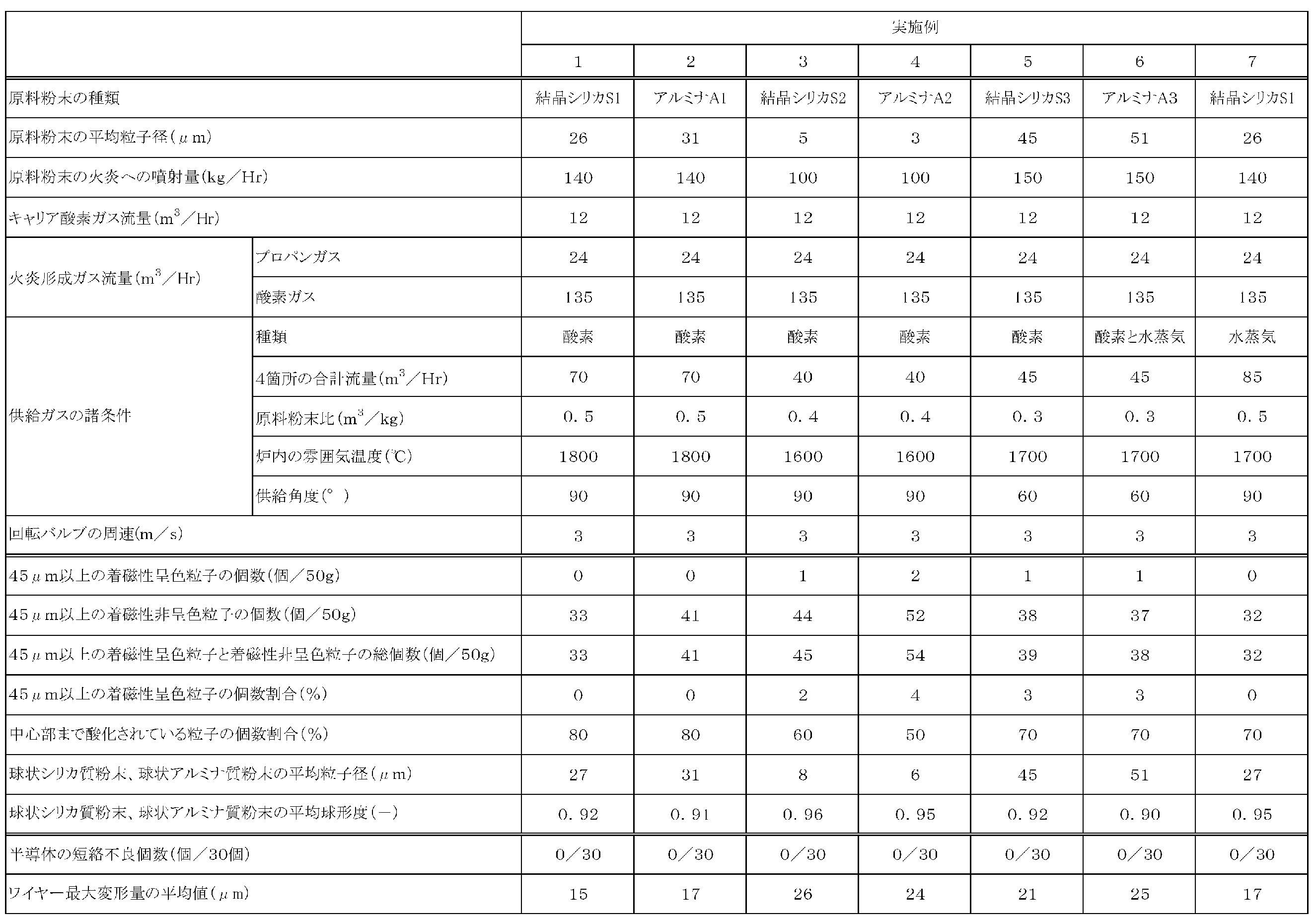
- Examples 1-7, Comparative Examples 1-9 Commercially available crystalline silica powder S1 (average particle diameter 26 ⁇ m), S2 (average particle diameter 5 ⁇ m), S3 (average particle diameter 45 ⁇ m), alumina powder A1 (average particle diameter 31 ⁇ m), A2 (average particle diameter 3 ⁇ m) shown in Table 1 ), A3 (average particle size 51 ⁇ m) was prepared. These raw material powders were melted and spheroidized in a flame under the production conditions described in Tables 2 and 3, and various spherical siliceous powders and spherical alumina powders were produced.
- the apparatus used is obtained by adding the following improvements (a) to (d) to the apparatus described in FIG. 1 of JP-A-11-57451. In Comparative Example 9, an apparatus without these improvements was used.
- (B) The mounting angle is powdered on the same circumference of the furnace body in which the atmospheric temperature in the furnace measured with a B-type thermocouple is either 1500 ° C, 1600 ° C, 1700 ° C, 1800 ° C or 1900 ° C.
- Oxygen gas and / or water vapor supply pipe adjusted by a bearing at 30 °, 60 °, 90 ° or 120 ° with respect to the raw material injection direction (downward direction in FIG. 1 of JP-A-11-57451) Was installed.
- the total number of supply pipes is four, and one supply pipe is installed at each position where the straight lines connecting the installation positions are orthogonal to each other.
- An alumina tube was used for the contact portion of the burner, and alumina brick was attached to the inner wall of the furnace body.
- C A portion where the relative speed between the powder and stainless steel and / or iron is 5 m / s or more, specifically, the exhaust communication port (reference numeral 9) in FIG. 1 of JP-A-11-57451, the primary powder The recovery port (symbol 10) and the secondary powder recovery port (symbol 11) were lined with alumina.
- the powder secondary recovery device bag filter (reference numeral 12) was lined with natural rubber.
- Oxygen gas and / or water vapor were supplied from each of the four supply pipes in an amount of 0 to 1.0 m 3 per 1 kg of the raw material powder in total.
- the temperature of the supplied oxygen gas was 20 ° C.
- the temperature of the water vapor gas was 105 to 110 ° C.
- the supply amount of the raw material powder was 100 to 170 kg / Hr.
- Propane gas and oxygen gas were used to form the flame.
- the maximum flame temperature was about 2000 ° C. to 2100 ° C. above the melting point of alumina.
- the number of magnetized non-colored particles was measured.
- the average sphericity and average particle diameter of the spherical siliceous powder and the spherical alumina powder were measured. The results are shown in Tables 1 and 2.
- the amorphous ratio of the spherical siliceous powder was 99% by mass or more.
- the kneaded product was pressed with a press machine and cooled, and then pulverized and tableted to produce semiconductor encapsulant tablets (17 mm ⁇ , 32 mmH), and the number of semiconductor short-circuit defects was evaluated as follows.
- all the parts in contact with each material were formed of any material of alumina, tungsten carbide, and urethane.
- a semiconductor element of size 8 mm x 8 mm x 0.3 mm is placed on a BGA substrate via a die attach film, connected to the substrate with a gold wire, and then a semiconductor encapsulant tablet is packaged using a transfer molding machine. After forming into 38 mm ⁇ 38 mm ⁇ 1.0 mm, after-curing at 175 ° C. for 8 hours, a BGA type semiconductor was produced. The diameter of the gold wire is ⁇ 20 ⁇ m, the pitch is 80 ⁇ m, and the interval is 60 ⁇ m. Thirty semiconductors were manufactured using the same semiconductor encapsulant tablet, and the number of semiconductors in which a short circuit failure occurred was counted.
- the semiconductor encapsulant containing the spherical siliceous powder and / or the spherical alumina powder of the present invention is the number of semiconductor short-circuit defects when the semiconductor is encapsulated. Can be significantly reduced. According to the powder composed of the spherical siliceous powder and / or the spherical alumina powder of the present invention, it is possible to provide a semiconductor sealing material that is suitably used for a miniaturized and densified semiconductor.
- the powder composed of the spherical siliceous powder and / or the spherical alumina powder of the present invention is filled in a semiconductor encapsulant used for automobiles, portable electronic devices, personal computers, home appliances, laminated boards on which semiconductors are mounted, etc. Used as a material.
- the resin composition of the present invention is used as a prepreg for printed circuit boards, various engineering plastics, and the like obtained by impregnating and curing glass woven fabric, glass nonwoven fabric, and other organic base materials in addition to the semiconductor sealing material. it can.
Landscapes
- Chemical & Material Sciences (AREA)
- Organic Chemistry (AREA)
- Inorganic Chemistry (AREA)
- Life Sciences & Earth Sciences (AREA)
- Geology (AREA)
- Chemical Kinetics & Catalysis (AREA)
- Health & Medical Sciences (AREA)
- Plasma & Fusion (AREA)
- Physics & Mathematics (AREA)
- Engineering & Computer Science (AREA)
- Medicinal Chemistry (AREA)
- Polymers & Plastics (AREA)
- Silicon Compounds (AREA)
- Compositions Of Macromolecular Compounds (AREA)
- Compounds Of Alkaline-Earth Elements, Aluminum Or Rare-Earth Metals (AREA)
- Powder Metallurgy (AREA)
Abstract
Description
(1)50gの粉末試料を精秤し、それをイオン交換水800gに分散させてスラリーを調製する。
(2)厚み20μmのゴム製カバーを被せた10000ガウスの棒磁石を、上記スラリーに浸漬して着磁性粒子を捕獲し、それを目開き45μmのポリエステル製フィルターで篩う。フイルター上に残った粒子を、「粒子径が45μm以上の着磁性呈色粒子と粒子径が45μm以上の着磁性非呈色粒子との総個数」とみなし、その個数を数える。
(3)上記フイルター上の粒子に、20℃の室温下、塩酸10質量%水溶液、プロピレングリコール50質量%水溶液およびフェリシアン化カリウム0.5質量%水溶液の等質量混合溶液を約0.5ml滴下して粒子を湿潤させ、20分間放置する。その結果、呈色した粒子を「粒子径が45μm以上の着磁性呈色粒子」とみなし、その個数を数える。式、(粒子径が45μm以上の着磁性呈色粒子の個数)×100/(粒子径が45μm以上の着磁性呈色粒子と粒子径が45μm以上の着磁性非呈色粒子の総個数)、により、粒子径が45μm以上の着磁性粒子に存在する粒子径が45μm以上の着磁性呈色粒子の個数割合を算出する。
(4)つぎに、呈色反応試験を終えた粒子径が45μm以上の着磁性非呈色粒子を選び、エポキシ樹脂で包埋し硬化させた後、切断・研磨して粒子断面を露出させ、断面の中心に存在する酸素の有無をエネルギー分散型X線分光器(EDS)で分析する。その結果、断面の中心から酸素が検出された粒子を「中心部まで酸化されている粒子」とみなし、その個数を数える。式、(中心部まで酸化されている粒子の個数)×100/(粒子径が45μm以上の着磁性非呈色粒子の個数)、により、粒子径が45μm以上の着磁性非呈色粒子に存在する中心部まで酸化されている粒子の個数割合を算出する。なお、EDSの分析条件は、加速電圧15kV、照射電流10nA、倍率2000倍、画素あたりの積算時間100msec、画素サイズ0.2μm□、画素数256×256pixelsである。
非晶質率(質量%)=(1-結晶質シリカ混在比)×100
から非晶質率を求めることができる。
低応力化剤として、シリコーンゴム、ポリサルファイドゴム、アクリル系ゴム、ブタジエン系ゴム、スチレン系ブロックコポリマーや飽和型エラストマー等のゴム状物質、各種熱可塑性樹脂、シリコーン樹脂等の樹脂状物質、更にはエポキシ樹脂、フェノール樹脂の一部又は全部がアミノシリコーン、エポキシシリコーン、アルコキシシリコーンなどで変性された樹脂など、
シランカップリング剤として、γ-グリシドキシプロピルトリメトキシシラン、β-(3,4-エポキシシクロヘキシル)エチルトリメトキシシラン等のエポキシシラン、アミノプロピルトリエトキシシラン、ウレイドプロピルトリエトキシシラン、N-フェニルアミノプロピルトリメトキシシラン等のアミノシラン、フェニルトリメトキシシラン、メチルトリメトキシシラン、オクタデシルトリメトキシシラン等の疎水性シラン化合物やメルカプトシランなど、
表面処理剤として、Zrキレート、チタネートカップリング剤、アルミニウム系カップリング剤など、
難燃助剤として、Sb2O3、Sb2O4、Sb2O5など、難燃剤として、ハロゲン化エポキシ樹脂やリン化合物など、
着色剤として、カーボンブラック、酸化鉄、染料、顔料など、
離型剤として、天然ワックス類、合成ワックス類、直鎖脂肪酸の金属塩、酸アミド類、エステル類、パラフィンなどが挙げられる。
表1に示される市販の結晶シリカ粉末S1(平均粒子径26μm)、S2(平均粒子径5μm)、S3(平均粒子径45μm)、アルミナ粉末A1(平均粒子径31μm)、A2(平均粒子径3μm)、A3(平均粒子径51μm)を用意した。これらの原料粉末を、表2及び表3に記載された製造条件にて火炎中で溶融、球状化し、種々の球状シリカ質粉末、球状アルミナ質粉末を製造した。
(イ)B型熱電対で測定された炉内の雰囲気温度が1500℃、1600℃、1700℃、1800℃又は1900℃のいずれかとなっている炉体の同一円周上に、取付角度を粉末原料の噴射方向(特開平11-57451号公報の図1における下方向)に対し30°、60°、90°又は120°のいずれかにベアリングで調節して酸素ガス及び/又は水蒸気の供給管を設置した。供給管の設置本数は合計4本であり、設置位置を結ぶ直線が直交するような位置にそれぞれ1本ずつ設置した。
(ロ)バーナーの接粉部には、アルミナ製の管を使用し、炉体の内壁にはアルミナレンガを貼りつけた。
(ハ)粉末とステンレス鋼及び/又は鉄との相対速度が5m/s以上となる部分、具体的には、特開平11-57451号公報の図1の排気連絡口(符合9)、粉末一次回収口(符合10)、粉末二次回収口(符合11)をアルミナでライニングした。また、粉末二次回収装置バッグフィルター(符合12)を天然ゴムでライニングした。
(ニ)粉末二次回収口の出口に設置したステンレスSUS304製の回転バルブの周速を1~18m/sの間に調整した。なお、本試験においては、粉末一次回収口は使用せず閉じたままとし、すべての粉末は粉末二次回収口より回収した。
各粉末87.8部(質量部、以下同じ)に対し、ビフェニル型エポキシ樹脂(ジャパンエポキシレジン社製YX-4000H)5.9部、フェノールアラルキル樹脂(三井化学社製XLC-LL)5.1部、トリフェニルホスフィン0.2部、メルカプトシランカップリング剤0.6部、カーボンブラック0.1部、カルナバワックス0.3部を加え、ヘンシェルミキサーにてドライブレンドした後、同方向噛み合い二軸押出混練機(スクリュー径D=25mm、ニーディングディスク長10Dmm、パドル回転数50~120rpm、吐出量2.5kg/Hr、混練物温度99~100℃)で加熱し混練した。混練物をプレス機にてプレスして冷却した後、粉砕、打錠して半導体封止材のタブレット(17mmφ、32mmH)を作製し、半導体の短絡不良個数を以下に従って評価した。なお、半導体封止材を作製するための設備及び器具からの着磁性粒子の混入を避けるため、各材料が接する部位は、すべてアルミナ、タングステンカーバイド、ウレタンのいずれかの材質で形成した。
BGA用基板に、ダイアタッチフィルムを介して、サイズ8mm×8mm×0.3mmの半導体素子を載せ、金ワイヤーで基板と接続した後、トランスファー成形機を用いて、半導体封止材タブレットをパッケージサイズ38mm×38mm×1.0mmに成形した後、175℃で8時間アフターキュアし、BGA型半導体を作製した。なお、金ワイヤーの径はφ20μm、ピッチは80μm、間隔は60μmである。同じ半導体封止材タブレットを用いて30個の半導体を作製し、短絡不良が起きた半導体の個数をカウントした。
上記で作製したBGA型半導体の金ワイヤーの部分を軟X線透過装置で観察し、パッケージングにより金ワイヤーが流された最大距離を30個の半導体について測定し、30本の金ワイヤーの最大流れ距離の平均値を求め、ワイヤー変形量とした。


Claims (9)
- 以下の(1)~(3)からなる呈色反応試験を行ったときに、粒子径が45μm以上の着磁性呈色粒子の個数割合が、粒子径が45μm以上の着磁性呈色粒子と粒子径が45μm以上の着磁性非呈色粒子との総個数に対して20%以下である、球状シリカ質粉末及び/又は球状アルミナ質粉末からなる粉末。
(1)50gの粉末試料を精秤し、それをイオン交換水800gに分散させてスラリーを調製する。
(2)厚み20μmのゴム製カバーを被せた10000ガウスの棒磁石を、上記スラリーに浸漬して着磁性粒子を捕獲し、それを目開き45μmのポリエステル製フィルターで篩う。フイルター上に残った粒子の個数を数え、その個数を「粒子径が45μm以上の着磁性呈色粒子と粒子径が45μm以上の着磁性非呈色粒子との総個数」とみなす。
(3)上記フイルター上の粒子に、20℃の室温下、塩酸10質量%水溶液、プロピレングリコール50質量%水溶液およびフェリシアン化カリウム0.5質量%水溶液の等質量混合溶液を約0.5ml滴下して粒子を湿潤させ、20分間放置する。その結果、呈色した粒子を「粒子径が45μm以上の着磁性呈色粒子」とみなし、その個数を数える。式、(粒子径が45μm以上の着磁性呈色粒子の個数)×100/(粒子径が45μm以上の着磁性呈色粒子と粒子径が45μm以上の着磁性非呈色粒子との総個数)、により、粒子径が45μm以上の着磁性粒子に存在する粒子径が45μm以上の着磁性呈色粒子の個数割合を算出する。 - 粒子径が45μm以上の着磁性呈色粒子の個数が、粉末50gあたり5個以下である請求項1記載の粉末。
- 粒子径が45μm以上の着磁性呈色粒子と粒子径が45μm以上の着磁性非呈色粒子との総個数が、粉末50gあたり50個以下である請求項1又は2記載の粉末。
- 前記呈色反応試験の後に以下の(4)を行って算出される、中心部まで酸化されている粒子の個数割合が、60%以上である請求項1~3のいずれかに記載の粉末。
(4)呈色反応試験を終えた粒子径が45μm以上の着磁性非呈色粒子を選び、エポキシ樹脂で包埋し硬化させた後、切断・研磨して粒子断面を露出させ、断面の中心に存在する酸素の有無をエネルギー分散型X線分光器(EDS)で分析する。その結果、断面の中心から酸素が検出された粒子を「中心部まで酸化されている粒子」とみなし、その個数を数える。式、(中心部まで酸化されている粒子の個数)×100/(粒子径が45μm以上の着磁性非呈色粒子の個数)、により、粒子径が45μm以上の着磁性非呈色粒子に存在する中心部まで酸化されている粒子の個数割合を算出する。なお、EDSの分析条件は、加速電圧15kV、照射電流10nA、倍率2000倍、画素あたりの積算時間100msec、画素サイズ0.2μm□、画素数256×256pixelsである。 - (4)を行って算出される、中心部まで酸化されている粒子の個数割合が、70%以上である請求項4記載の粉末。
- 粉末の平均球形度が0.75以上で、平均粒子径が3~50μmである請求項1~5のいずれか記載の粉末。
- シリカ質粉末原料及び/又はアルミナ質粉末原料を炉内に形成された火炎で溶融し、球状化処理した後、炉外に搬送して球状粉末を捕集する工程を有し、この工程が、炉内のうち雰囲気温度が1600~1800℃となっている任意の少なくとも1個所に、原料粉末1kgあたり0.3~0.6m3の酸素ガス及び/又は水蒸気を、粉末原料の噴射方向に対し60°~90°の角度にて供給する工程、及び、粉末原料の溶融、球状化処理から球状粉末の捕集までの間において、粉末原料及び/又は球状粉末とステンレス鋼及び/又は鉄とが接触する部分におけるこれらの相対速度を5m/s以下にする工程を有する、球状シリカ質粉末及び/又は球状アルミナ質粉末からなる粉末の製造方法。
- 球状シリカ質粉末及び/又は球状アルミナ質粉末からなる粉末が、請求項1~6のいずれか記載の粉末である請求項7記載の製造方法。
- 請求項1~6のいずれか記載の粉末を含有してなる樹脂組成物。
Priority Applications (4)
| Application Number | Priority Date | Filing Date | Title |
|---|---|---|---|
| CN200980157321.XA CN102325724B (zh) | 2008-12-22 | 2009-10-29 | 粉末、其制造方法及包含该粉末的树脂组合物 |
| JP2010543771A JP5555639B2 (ja) | 2008-12-22 | 2009-10-29 | 粉末、その製造方法、及びその粉末を含む樹脂組成物 |
| SG2011045127A SG172279A1 (en) | 2008-12-22 | 2009-10-29 | Powder, method for producing same, and resin composition containing same |
| US13/141,133 US20110300384A1 (en) | 2008-12-22 | 2009-10-29 | Powder, method for producing same, and resin composition containing same |
Applications Claiming Priority (2)
| Application Number | Priority Date | Filing Date | Title |
|---|---|---|---|
| JP2008324881 | 2008-12-22 | ||
| JP2008-324881 | 2008-12-22 |
Publications (1)
| Publication Number | Publication Date |
|---|---|
| WO2010073457A1 true WO2010073457A1 (ja) | 2010-07-01 |
Family
ID=42287120
Family Applications (1)
| Application Number | Title | Priority Date | Filing Date |
|---|---|---|---|
| PCT/JP2009/005730 Ceased WO2010073457A1 (ja) | 2008-12-22 | 2009-10-29 | 粉末、その製造方法、及びその粉末を含む樹脂組成物 |
Country Status (8)
| Country | Link |
|---|---|
| US (1) | US20110300384A1 (ja) |
| JP (1) | JP5555639B2 (ja) |
| KR (1) | KR101647862B1 (ja) |
| CN (1) | CN102325724B (ja) |
| MY (1) | MY155608A (ja) |
| SG (1) | SG172279A1 (ja) |
| TW (1) | TWI483897B (ja) |
| WO (1) | WO2010073457A1 (ja) |
Cited By (3)
| Publication number | Priority date | Publication date | Assignee | Title |
|---|---|---|---|---|
| JP2012206870A (ja) * | 2011-03-29 | 2012-10-25 | Admatechs Co Ltd | 球状シリカ粉体の製造方法及び半導体封止材の製造方法 |
| JP2015086120A (ja) * | 2013-10-31 | 2015-05-07 | 株式会社トクヤマ | 球状シリカ微粉末とその製造方法 |
| JP2023036470A (ja) * | 2021-09-02 | 2023-03-14 | デンカ株式会社 | 無機酸化物粒子の製造方法 |
Families Citing this family (7)
| Publication number | Priority date | Publication date | Assignee | Title |
|---|---|---|---|---|
| CN104157581B (zh) * | 2014-07-23 | 2017-03-15 | 西安空间无线电技术研究所 | 一种功率二极管二次封装方法 |
| KR101900549B1 (ko) * | 2015-06-30 | 2018-09-19 | 삼성에스디아이 주식회사 | 과립상 반도체 소자 봉지용 에폭시 수지 조성물 및 이를 사용하여 봉지된 반도체 소자 |
| KR102578962B1 (ko) * | 2018-01-26 | 2023-09-14 | 덴카 주식회사 | 비정질 실리카 분말 및 그 제조 방법, 용도 |
| CN111065603B (zh) * | 2018-08-17 | 2021-04-23 | 浙江三时纪新材科技有限公司 | 一种半导体封装材料的制备方法以及由此得到的半导体封装材料 |
| JP7543394B2 (ja) * | 2020-03-31 | 2024-09-02 | デンカ株式会社 | アルミナ粉末、フィラー組成物、樹脂組成物、封止材、及び指紋認証センサー |
| TWI744067B (zh) * | 2020-11-02 | 2021-10-21 | 財團法人工業技術研究院 | 粉體圓球化設備 |
| KR102810250B1 (ko) * | 2024-04-11 | 2025-05-23 | (주)샘씨엔에스 | 구속용 시트, 이의 제조 방법 및 이를 이용한 다층 세라믹 기판 제조 방법 |
Citations (6)
| Publication number | Priority date | Publication date | Assignee | Title |
|---|---|---|---|---|
| JPH1157451A (ja) * | 1997-08-25 | 1999-03-02 | Denki Kagaku Kogyo Kk | 無機質球状粒子の製造方法及び装置 |
| JPH1171107A (ja) * | 1997-08-25 | 1999-03-16 | Denki Kagaku Kogyo Kk | 無機質球状粒子の製造方法及び装置 |
| JP2000178413A (ja) * | 1998-12-16 | 2000-06-27 | Tokuyama Corp | 半導体封止材用球状シリカ |
| JP2005281063A (ja) * | 2004-03-30 | 2005-10-13 | Denki Kagaku Kogyo Kk | 高純度球状アルミナ粉末、その製造方法及び組成物 |
| JP2005306923A (ja) * | 2004-04-19 | 2005-11-04 | Denki Kagaku Kogyo Kk | 無機質粉末及びこれを含有した組成物 |
| JP2008145246A (ja) * | 2006-12-08 | 2008-06-26 | Denki Kagaku Kogyo Kk | 非磁性金属酸化物粉末における着磁性粒子の個数測定方法 |
Family Cites Families (11)
| Publication number | Priority date | Publication date | Assignee | Title |
|---|---|---|---|---|
| JPH06106524A (ja) | 1992-09-24 | 1994-04-19 | Tokyo Seimitsu Co Ltd | 半導体ウエハのスライシング方法 |
| KR100388141B1 (ko) * | 1995-07-10 | 2003-10-17 | 도레이 가부시끼가이샤 | 에폭시수지조성물 |
| JP3446951B2 (ja) * | 1999-11-15 | 2003-09-16 | 電気化学工業株式会社 | 無機質粉末及びそれが充填された樹脂組成物 |
| JP4294191B2 (ja) | 2000-02-22 | 2009-07-08 | 電気化学工業株式会社 | 球状シリカ粉末の製造方法及び製造装置 |
| CN1436819A (zh) * | 2002-02-07 | 2003-08-20 | 户田工业株式会社 | 半导体密封材料用黑色复合颗粒和半导体密封材料 |
| JP2004175825A (ja) | 2002-11-25 | 2004-06-24 | Matsushita Electric Works Ltd | 封止材料の製造方法およびこれにより製造した封止材料 |
| JP4083560B2 (ja) * | 2002-12-13 | 2008-04-30 | 株式会社トクヤマ | 絶縁特性が改善された無機酸化物粒子の製造方法 |
| US7112393B2 (en) * | 2003-07-29 | 2006-09-26 | Canon Kabushiki Kaisha | Non-magnetic toner |
| DE102004051671A1 (de) * | 2004-10-22 | 2006-04-27 | Microdyn-Nadir Gmbh | Vorrichtung zum Filtern von Stoffen aus Flüssigkeiten |
| JP2006124478A (ja) * | 2004-10-27 | 2006-05-18 | Nitto Denko Corp | 半導体封止用エポキシ樹脂組成物およびそれを用いた半導体装置 |
| JP2007005346A (ja) | 2005-06-21 | 2007-01-11 | Sanyu Rec Co Ltd | 金属性異物の除去方法 |
-
2009
- 2009-10-29 MY MYPI2011002903A patent/MY155608A/en unknown
- 2009-10-29 WO PCT/JP2009/005730 patent/WO2010073457A1/ja not_active Ceased
- 2009-10-29 US US13/141,133 patent/US20110300384A1/en not_active Abandoned
- 2009-10-29 KR KR1020117016922A patent/KR101647862B1/ko active Active
- 2009-10-29 SG SG2011045127A patent/SG172279A1/en unknown
- 2009-10-29 CN CN200980157321.XA patent/CN102325724B/zh active Active
- 2009-10-29 JP JP2010543771A patent/JP5555639B2/ja active Active
- 2009-12-17 TW TW098143268A patent/TWI483897B/zh not_active IP Right Cessation
Patent Citations (6)
| Publication number | Priority date | Publication date | Assignee | Title |
|---|---|---|---|---|
| JPH1157451A (ja) * | 1997-08-25 | 1999-03-02 | Denki Kagaku Kogyo Kk | 無機質球状粒子の製造方法及び装置 |
| JPH1171107A (ja) * | 1997-08-25 | 1999-03-16 | Denki Kagaku Kogyo Kk | 無機質球状粒子の製造方法及び装置 |
| JP2000178413A (ja) * | 1998-12-16 | 2000-06-27 | Tokuyama Corp | 半導体封止材用球状シリカ |
| JP2005281063A (ja) * | 2004-03-30 | 2005-10-13 | Denki Kagaku Kogyo Kk | 高純度球状アルミナ粉末、その製造方法及び組成物 |
| JP2005306923A (ja) * | 2004-04-19 | 2005-11-04 | Denki Kagaku Kogyo Kk | 無機質粉末及びこれを含有した組成物 |
| JP2008145246A (ja) * | 2006-12-08 | 2008-06-26 | Denki Kagaku Kogyo Kk | 非磁性金属酸化物粉末における着磁性粒子の個数測定方法 |
Cited By (3)
| Publication number | Priority date | Publication date | Assignee | Title |
|---|---|---|---|---|
| JP2012206870A (ja) * | 2011-03-29 | 2012-10-25 | Admatechs Co Ltd | 球状シリカ粉体の製造方法及び半導体封止材の製造方法 |
| JP2015086120A (ja) * | 2013-10-31 | 2015-05-07 | 株式会社トクヤマ | 球状シリカ微粉末とその製造方法 |
| JP2023036470A (ja) * | 2021-09-02 | 2023-03-14 | デンカ株式会社 | 無機酸化物粒子の製造方法 |
Also Published As
| Publication number | Publication date |
|---|---|
| MY155608A (en) | 2015-11-13 |
| JPWO2010073457A1 (ja) | 2012-05-31 |
| US20110300384A1 (en) | 2011-12-08 |
| CN102325724A (zh) | 2012-01-18 |
| KR101647862B1 (ko) | 2016-08-11 |
| SG172279A1 (en) | 2011-07-28 |
| TW201031593A (en) | 2010-09-01 |
| TWI483897B (zh) | 2015-05-11 |
| JP5555639B2 (ja) | 2014-07-23 |
| KR20110106891A (ko) | 2011-09-29 |
| CN102325724B (zh) | 2014-02-12 |
Similar Documents
| Publication | Publication Date | Title |
|---|---|---|
| JP5555639B2 (ja) | 粉末、その製造方法、及びその粉末を含む樹脂組成物 | |
| CN101472840B (zh) | 陶瓷粉末及其用途 | |
| JP4306951B2 (ja) | 表面処理された微細球状シリカ粉末および樹脂組成物 | |
| JP5354724B2 (ja) | セラミックス粉末及びその用途 | |
| JP2001048521A (ja) | 微細球状シリカ粉末とその製造方法および用途 | |
| JPWO2009017058A1 (ja) | シリカ粉末、その製造方法及びそれを用いた組成物 | |
| CN102066254B (zh) | 无定形二氧化硅粉末、其制造方法、树脂组合物及半导体密封材料 | |
| CN101563291B (zh) | 无定形二氧化硅粉末、其制造方法及半导体密封材料 | |
| JP4192073B2 (ja) | シリカ粉末の製造方法 | |
| JP2001139725A (ja) | 無機質粉末及びそれが充填された樹脂組成物 | |
| EP3744685B1 (en) | Amorphous silica powder, production method therefor, and use thereof | |
| JP5085432B2 (ja) | 着磁性異物を低減した球状金属酸化物粉末、その製造方法及び用途 | |
| JP2001158614A (ja) | 球状無機質粉末及びその用途 | |
| JP2005306923A (ja) | 無機質粉末及びこれを含有した組成物 | |
| TWI457281B (zh) | 氧化矽質粉末、其製造方法及用途 | |
| JP6612919B2 (ja) | 非晶質シリカ粉末、樹脂組成物、及び半導体封止材 | |
| JP2003146648A (ja) | 球状無機質粉末およびこれを充填した樹脂組成物 | |
| JP3571009B2 (ja) | 球状無機質粉末およびこれを充填した樹脂組成物 | |
| JP5345787B2 (ja) | 半導体封止材用シリカ・アルミナ複合酸化物超微粉末の製造方法 | |
| TWI411594B (zh) | 陶瓷粉末及其用途 | |
| JP2001039709A (ja) | シリカ質粉末及び樹脂組成物 |
Legal Events
| Date | Code | Title | Description |
|---|---|---|---|
| WWE | Wipo information: entry into national phase |
Ref document number: 200980157321.X Country of ref document: CN |
|
| 121 | Ep: the epo has been informed by wipo that ep was designated in this application |
Ref document number: 09834274 Country of ref document: EP Kind code of ref document: A1 |
|
| ENP | Entry into the national phase |
Ref document number: 2010543771 Country of ref document: JP Kind code of ref document: A |
|
| NENP | Non-entry into the national phase |
Ref country code: DE |
|
| ENP | Entry into the national phase |
Ref document number: 20117016922 Country of ref document: KR Kind code of ref document: A |
|
| WWE | Wipo information: entry into national phase |
Ref document number: 13141133 Country of ref document: US |
|
| 122 | Ep: pct application non-entry in european phase |
Ref document number: 09834274 Country of ref document: EP Kind code of ref document: A1 |