WO2010067704A1 - 光起電力装置及びその製造方法 - Google Patents
光起電力装置及びその製造方法 Download PDFInfo
- Publication number
- WO2010067704A1 WO2010067704A1 PCT/JP2009/069838 JP2009069838W WO2010067704A1 WO 2010067704 A1 WO2010067704 A1 WO 2010067704A1 JP 2009069838 W JP2009069838 W JP 2009069838W WO 2010067704 A1 WO2010067704 A1 WO 2010067704A1
- Authority
- WO
- WIPO (PCT)
- Prior art keywords
- solar cell
- electrode
- cell unit
- intermediate layer
- photovoltaic device
- Prior art date
- Legal status (The legal status is an assumption and is not a legal conclusion. Google has not performed a legal analysis and makes no representation as to the accuracy of the status listed.)
- Ceased
Links
Images
Classifications
-
- H—ELECTRICITY
- H10—SEMICONDUCTOR DEVICES; ELECTRIC SOLID-STATE DEVICES NOT OTHERWISE PROVIDED FOR
- H10F—INORGANIC SEMICONDUCTOR DEVICES SENSITIVE TO INFRARED RADIATION, LIGHT, ELECTROMAGNETIC RADIATION OF SHORTER WAVELENGTH OR CORPUSCULAR RADIATION
- H10F10/00—Individual photovoltaic cells, e.g. solar cells
- H10F10/10—Individual photovoltaic cells, e.g. solar cells having potential barriers
- H10F10/17—Photovoltaic cells having only PIN junction potential barriers
- H10F10/172—Photovoltaic cells having only PIN junction potential barriers comprising multiple PIN junctions, e.g. tandem cells
-
- H—ELECTRICITY
- H10—SEMICONDUCTOR DEVICES; ELECTRIC SOLID-STATE DEVICES NOT OTHERWISE PROVIDED FOR
- H10F—INORGANIC SEMICONDUCTOR DEVICES SENSITIVE TO INFRARED RADIATION, LIGHT, ELECTROMAGNETIC RADIATION OF SHORTER WAVELENGTH OR CORPUSCULAR RADIATION
- H10F19/00—Integrated devices, or assemblies of multiple devices, comprising at least one photovoltaic cell covered by group H10F10/00, e.g. photovoltaic modules
- H10F19/30—Integrated devices, or assemblies of multiple devices, comprising at least one photovoltaic cell covered by group H10F10/00, e.g. photovoltaic modules comprising thin-film photovoltaic cells
- H10F19/31—Integrated devices, or assemblies of multiple devices, comprising at least one photovoltaic cell covered by group H10F10/00, e.g. photovoltaic modules comprising thin-film photovoltaic cells having multiple laterally adjacent thin-film photovoltaic cells deposited on the same substrate
- H10F19/33—Patterning processes to connect the photovoltaic cells, e.g. laser cutting of conductive or active layers
-
- H—ELECTRICITY
- H10—SEMICONDUCTOR DEVICES; ELECTRIC SOLID-STATE DEVICES NOT OTHERWISE PROVIDED FOR
- H10F—INORGANIC SEMICONDUCTOR DEVICES SENSITIVE TO INFRARED RADIATION, LIGHT, ELECTROMAGNETIC RADIATION OF SHORTER WAVELENGTH OR CORPUSCULAR RADIATION
- H10F19/00—Integrated devices, or assemblies of multiple devices, comprising at least one photovoltaic cell covered by group H10F10/00, e.g. photovoltaic modules
- H10F19/40—Integrated devices, or assemblies of multiple devices, comprising at least one photovoltaic cell covered by group H10F10/00, e.g. photovoltaic modules comprising photovoltaic cells in a mechanically stacked configuration
-
- Y—GENERAL TAGGING OF NEW TECHNOLOGICAL DEVELOPMENTS; GENERAL TAGGING OF CROSS-SECTIONAL TECHNOLOGIES SPANNING OVER SEVERAL SECTIONS OF THE IPC; TECHNICAL SUBJECTS COVERED BY FORMER USPC CROSS-REFERENCE ART COLLECTIONS [XRACs] AND DIGESTS
- Y02—TECHNOLOGIES OR APPLICATIONS FOR MITIGATION OR ADAPTATION AGAINST CLIMATE CHANGE
- Y02E—REDUCTION OF GREENHOUSE GAS [GHG] EMISSIONS, RELATED TO ENERGY GENERATION, TRANSMISSION OR DISTRIBUTION
- Y02E10/00—Energy generation through renewable energy sources
- Y02E10/50—Photovoltaic [PV] energy
- Y02E10/548—Amorphous silicon PV cells
Definitions
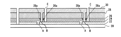
- the solar cell unit as a power generation layer is exposed to oxygen, resulting in a new problem that the characteristics of the solar cell unit itself deteriorate.
- the first separation groove A is formed in the surface electrode 22.
- the separation groove A is formed by laser processing, for example.
- an Nd: YAG laser having a wavelength of about 1064 nm and an energy density of 1 ⁇ 10 5 W / cm 2 is used.
- the line width of the separation groove A is preferably 10 ⁇ m or more and 200 ⁇ m or less.
Landscapes
- Photovoltaic Devices (AREA)
Priority Applications (1)
| Application Number | Priority Date | Filing Date | Title |
|---|---|---|---|
| US13/121,797 US20110197952A1 (en) | 2008-12-09 | 2009-11-25 | Photovoltaic device and manufacturing method for a photovoltaic device |
Applications Claiming Priority (2)
| Application Number | Priority Date | Filing Date | Title |
|---|---|---|---|
| JP2008313001A JP2010140935A (ja) | 2008-12-09 | 2008-12-09 | 光起電力装置及びその製造方法 |
| JP2008-313001 | 2008-12-09 |
Publications (1)
| Publication Number | Publication Date |
|---|---|
| WO2010067704A1 true WO2010067704A1 (ja) | 2010-06-17 |
Family
ID=42242694
Family Applications (1)
| Application Number | Title | Priority Date | Filing Date |
|---|---|---|---|
| PCT/JP2009/069838 Ceased WO2010067704A1 (ja) | 2008-12-09 | 2009-11-25 | 光起電力装置及びその製造方法 |
Country Status (3)
| Country | Link |
|---|---|
| US (1) | US20110197952A1 (https=) |
| JP (1) | JP2010140935A (https=) |
| WO (1) | WO2010067704A1 (https=) |
Families Citing this family (2)
| Publication number | Priority date | Publication date | Assignee | Title |
|---|---|---|---|---|
| CN102456757A (zh) * | 2010-10-26 | 2012-05-16 | 富阳光电股份有限公司 | 多层堆栈结构的半导体元件 |
| WO2013041467A1 (de) * | 2011-09-19 | 2013-03-28 | Saint-Gobain Glass France | Dünnschichtsolarmodul mit serienverschaltung und verfahren zur serienverschaltung von dünnschichtsolarzellen |
Citations (11)
| Publication number | Priority date | Publication date | Assignee | Title |
|---|---|---|---|---|
| JPS6237920U (https=) * | 1985-08-26 | 1987-03-06 | ||
| JPS6384074A (ja) * | 1986-09-26 | 1988-04-14 | Sanyo Electric Co Ltd | 光起電力装置 |
| JPH09162431A (ja) * | 1995-12-13 | 1997-06-20 | Kanegafuchi Chem Ind Co Ltd | 並列型集積化太陽電池 |
| JPH11274527A (ja) * | 1998-03-24 | 1999-10-08 | Sanyo Electric Co Ltd | 光起電力装置 |
| JP2001068707A (ja) * | 1999-08-27 | 2001-03-16 | Univ Osaka | 導電性材料、導電性薄膜、複合膜、及び導電性材料の製造方法 |
| JP2003273383A (ja) * | 2002-03-15 | 2003-09-26 | Sharp Corp | 太陽電池素子およびその製造方法 |
| JP2005038907A (ja) * | 2003-07-15 | 2005-02-10 | Kyocera Corp | 集積型光電変換装置 |
| JP2005093939A (ja) * | 2003-09-19 | 2005-04-07 | Mitsubishi Heavy Ind Ltd | 集積型タンデム接合太陽電池及び集積型タンデム接合太陽電池の製造方法 |
| JP2005217038A (ja) * | 2004-01-28 | 2005-08-11 | Sanyo Electric Co Ltd | p型ZnO半導体膜及びその製造方法 |
| JP2005322707A (ja) * | 2004-05-07 | 2005-11-17 | Mitsubishi Heavy Ind Ltd | 集積型太陽電池 |
| JP2006313872A (ja) * | 2005-04-06 | 2006-11-16 | Mitsubishi Heavy Ind Ltd | 多接合薄膜太陽電池 |
-
2008
- 2008-12-09 JP JP2008313001A patent/JP2010140935A/ja active Pending
-
2009
- 2009-11-25 US US13/121,797 patent/US20110197952A1/en not_active Abandoned
- 2009-11-25 WO PCT/JP2009/069838 patent/WO2010067704A1/ja not_active Ceased
Patent Citations (11)
| Publication number | Priority date | Publication date | Assignee | Title |
|---|---|---|---|---|
| JPS6237920U (https=) * | 1985-08-26 | 1987-03-06 | ||
| JPS6384074A (ja) * | 1986-09-26 | 1988-04-14 | Sanyo Electric Co Ltd | 光起電力装置 |
| JPH09162431A (ja) * | 1995-12-13 | 1997-06-20 | Kanegafuchi Chem Ind Co Ltd | 並列型集積化太陽電池 |
| JPH11274527A (ja) * | 1998-03-24 | 1999-10-08 | Sanyo Electric Co Ltd | 光起電力装置 |
| JP2001068707A (ja) * | 1999-08-27 | 2001-03-16 | Univ Osaka | 導電性材料、導電性薄膜、複合膜、及び導電性材料の製造方法 |
| JP2003273383A (ja) * | 2002-03-15 | 2003-09-26 | Sharp Corp | 太陽電池素子およびその製造方法 |
| JP2005038907A (ja) * | 2003-07-15 | 2005-02-10 | Kyocera Corp | 集積型光電変換装置 |
| JP2005093939A (ja) * | 2003-09-19 | 2005-04-07 | Mitsubishi Heavy Ind Ltd | 集積型タンデム接合太陽電池及び集積型タンデム接合太陽電池の製造方法 |
| JP2005217038A (ja) * | 2004-01-28 | 2005-08-11 | Sanyo Electric Co Ltd | p型ZnO半導体膜及びその製造方法 |
| JP2005322707A (ja) * | 2004-05-07 | 2005-11-17 | Mitsubishi Heavy Ind Ltd | 集積型太陽電池 |
| JP2006313872A (ja) * | 2005-04-06 | 2006-11-16 | Mitsubishi Heavy Ind Ltd | 多接合薄膜太陽電池 |
Also Published As
| Publication number | Publication date |
|---|---|
| US20110197952A1 (en) | 2011-08-18 |
| JP2010140935A (ja) | 2010-06-24 |
Similar Documents
| Publication | Publication Date | Title |
|---|---|---|
| JP5774204B2 (ja) | 光起電力素子およびその製造方法、太陽電池モジュール | |
| CN1826699B (zh) | 硅类薄膜太阳能电池 | |
| EP2846363B1 (en) | Solar cell | |
| JP4928337B2 (ja) | 光電変換装置の製造方法 | |
| JP5602251B2 (ja) | 透明電極基板およびその製造方法、光電変換装置およびその製造方法、光電変換モジュール | |
| JP2005135987A (ja) | 積層型光電変換装置及びその製造方法 | |
| JP4975528B2 (ja) | 集積形太陽電池 | |
| JP4025744B2 (ja) | 積層型光電変換装置の製造方法 | |
| JP5400322B2 (ja) | シリコン系薄膜太陽電池およびその製造方法 | |
| JP2007035695A (ja) | 集積型薄膜太陽電池モジュール | |
| JP5180574B2 (ja) | 多接合型シリコン系薄膜光電変換装置 | |
| JP7344593B2 (ja) | 半導体装置および太陽電池並びに半導体装置の製造方法 | |
| WO2010067704A1 (ja) | 光起電力装置及びその製造方法 | |
| JP2008283075A (ja) | 光電変換装置の製造方法 | |
| JP2012253091A (ja) | 光起電力装置及びその製造方法 | |
| JP2007305826A (ja) | シリコン系薄膜太陽電池 | |
| JP2005135986A (ja) | 積層型光電変換装置 | |
| JP5232362B2 (ja) | 集積化薄膜光電変換装置の製造方法および、その製造方法で得られうる集積化薄膜光電変換装置。 | |
| JP5539081B2 (ja) | 集積型薄膜光電変換装置の製造方法 | |
| JP7699671B2 (ja) | 太陽電池及びその製造方法 | |
| JP2005244071A (ja) | 太陽電池およびその製造方法 | |
| WO2011105166A1 (ja) | 光電変換モジュール及びその製造方法 | |
| JP2010283162A (ja) | 太陽電池及びその製造方法 | |
| TWI647327B (zh) | 矽基疊層的形成方法及矽基異質接面太陽能電池的製造方法 | |
| JP5307280B2 (ja) | 薄膜光電変換素子 |
Legal Events
| Date | Code | Title | Description |
|---|---|---|---|
| 121 | Ep: the epo has been informed by wipo that ep was designated in this application |
Ref document number: 09831809 Country of ref document: EP Kind code of ref document: A1 |
|
| WWE | Wipo information: entry into national phase |
Ref document number: 13121797 Country of ref document: US |
|
| NENP | Non-entry into the national phase |
Ref country code: DE |
|
| 122 | Ep: pct application non-entry in european phase |
Ref document number: 09831809 Country of ref document: EP Kind code of ref document: A1 |