WO2010067517A1 - 半導体装置の製造方法 - Google Patents
半導体装置の製造方法 Download PDFInfo
- Publication number
- WO2010067517A1 WO2010067517A1 PCT/JP2009/006013 JP2009006013W WO2010067517A1 WO 2010067517 A1 WO2010067517 A1 WO 2010067517A1 JP 2009006013 W JP2009006013 W JP 2009006013W WO 2010067517 A1 WO2010067517 A1 WO 2010067517A1
- Authority
- WO
- WIPO (PCT)
- Prior art keywords
- film
- single crystal
- constituent element
- gas
- crystal silicon
- Prior art date
- Legal status (The legal status is an assumption and is not a legal conclusion. Google has not performed a legal analysis and makes no representation as to the accuracy of the status listed.)
- Ceased
Links
Images



Classifications
-
- H—ELECTRICITY
- H10—SEMICONDUCTOR DEVICES; ELECTRIC SOLID-STATE DEVICES NOT OTHERWISE PROVIDED FOR
- H10P—GENERIC PROCESSES OR APPARATUS FOR THE MANUFACTURE OR TREATMENT OF DEVICES COVERED BY CLASS H10
- H10P14/00—Formation of materials, e.g. in the shape of layers or pillars
- H10P14/20—Formation of materials, e.g. in the shape of layers or pillars of semiconductor materials
- H10P14/24—Formation of materials, e.g. in the shape of layers or pillars of semiconductor materials using chemical vapour deposition [CVD]
-
- H—ELECTRICITY
- H10—SEMICONDUCTOR DEVICES; ELECTRIC SOLID-STATE DEVICES NOT OTHERWISE PROVIDED FOR
- H10D—INORGANIC ELECTRIC SEMICONDUCTOR DEVICES
- H10D84/00—Integrated devices formed in or on semiconductor substrates that comprise only semiconducting layers, e.g. on Si wafers or on GaAs-on-Si wafers
- H10D84/01—Manufacture or treatment
- H10D84/02—Manufacture or treatment characterised by using material-based technologies
- H10D84/03—Manufacture or treatment characterised by using material-based technologies using Group IV technology, e.g. silicon technology or silicon-carbide [SiC] technology
- H10D84/038—Manufacture or treatment characterised by using material-based technologies using Group IV technology, e.g. silicon technology or silicon-carbide [SiC] technology using silicon technology, e.g. SiGe
-
- H—ELECTRICITY
- H10—SEMICONDUCTOR DEVICES; ELECTRIC SOLID-STATE DEVICES NOT OTHERWISE PROVIDED FOR
- H10D—INORGANIC ELECTRIC SEMICONDUCTOR DEVICES
- H10D86/00—Integrated devices formed in or on insulating or conducting substrates, e.g. formed in silicon-on-insulator [SOI] substrates or on stainless steel or glass substrates
- H10D86/201—Integrated devices formed in or on insulating or conducting substrates, e.g. formed in silicon-on-insulator [SOI] substrates or on stainless steel or glass substrates the substrates comprising an insulating layer on a semiconductor body, e.g. SOI
-
- H—ELECTRICITY
- H10—SEMICONDUCTOR DEVICES; ELECTRIC SOLID-STATE DEVICES NOT OTHERWISE PROVIDED FOR
- H10D—INORGANIC ELECTRIC SEMICONDUCTOR DEVICES
- H10D88/00—Three-dimensional [3D] integrated devices
-
- H—ELECTRICITY
- H10—SEMICONDUCTOR DEVICES; ELECTRIC SOLID-STATE DEVICES NOT OTHERWISE PROVIDED FOR
- H10D—INORGANIC ELECTRIC SEMICONDUCTOR DEVICES
- H10D88/00—Three-dimensional [3D] integrated devices
- H10D88/01—Manufacture or treatment
-
- H—ELECTRICITY
- H10—SEMICONDUCTOR DEVICES; ELECTRIC SOLID-STATE DEVICES NOT OTHERWISE PROVIDED FOR
- H10P—GENERIC PROCESSES OR APPARATUS FOR THE MANUFACTURE OR TREATMENT OF DEVICES COVERED BY CLASS H10
- H10P14/00—Formation of materials, e.g. in the shape of layers or pillars
- H10P14/20—Formation of materials, e.g. in the shape of layers or pillars of semiconductor materials
- H10P14/27—Formation of materials, e.g. in the shape of layers or pillars of semiconductor materials using selective deposition, e.g. simultaneous growth of monocrystalline and non-monocrystalline semiconductor materials
-
- H—ELECTRICITY
- H10—SEMICONDUCTOR DEVICES; ELECTRIC SOLID-STATE DEVICES NOT OTHERWISE PROVIDED FOR
- H10P—GENERIC PROCESSES OR APPARATUS FOR THE MANUFACTURE OR TREATMENT OF DEVICES COVERED BY CLASS H10
- H10P14/00—Formation of materials, e.g. in the shape of layers or pillars
- H10P14/20—Formation of materials, e.g. in the shape of layers or pillars of semiconductor materials
- H10P14/34—Deposited materials, e.g. layers
- H10P14/3402—Deposited materials, e.g. layers characterised by the chemical composition
- H10P14/3404—Deposited materials, e.g. layers characterised by the chemical composition being Group IVA materials
- H10P14/3411—Silicon, silicon germanium or germanium
-
- H—ELECTRICITY
- H10—SEMICONDUCTOR DEVICES; ELECTRIC SOLID-STATE DEVICES NOT OTHERWISE PROVIDED FOR
- H10P—GENERIC PROCESSES OR APPARATUS FOR THE MANUFACTURE OR TREATMENT OF DEVICES COVERED BY CLASS H10
- H10P72/00—Handling or holding of wafers, substrates or devices during manufacture or treatment thereof
- H10P72/30—Handling or holding of wafers, substrates or devices during manufacture or treatment thereof for conveying, e.g. between different workstations
- H10P72/33—Handling or holding of wafers, substrates or devices during manufacture or treatment thereof for conveying, e.g. between different workstations into and out of processing chamber
- H10P72/3312—Vertical transfer of a batch of workpieces
-
- H—ELECTRICITY
- H10—SEMICONDUCTOR DEVICES; ELECTRIC SOLID-STATE DEVICES NOT OTHERWISE PROVIDED FOR
- H10D—INORGANIC ELECTRIC SEMICONDUCTOR DEVICES
- H10D86/00—Integrated devices formed in or on insulating or conducting substrates, e.g. formed in silicon-on-insulator [SOI] substrates or on stainless steel or glass substrates
- H10D86/01—Manufacture or treatment
-
- H—ELECTRICITY
- H10—SEMICONDUCTOR DEVICES; ELECTRIC SOLID-STATE DEVICES NOT OTHERWISE PROVIDED FOR
- H10P—GENERIC PROCESSES OR APPARATUS FOR THE MANUFACTURE OR TREATMENT OF DEVICES COVERED BY CLASS H10
- H10P14/00—Formation of materials, e.g. in the shape of layers or pillars
- H10P14/20—Formation of materials, e.g. in the shape of layers or pillars of semiconductor materials
- H10P14/38—Formation of materials, e.g. in the shape of layers or pillars of semiconductor materials characterised by treatments done after the formation of the materials
- H10P14/3802—Crystallisation or recrystallisation of non-monocrystalline semiconductor materials, e.g. regrowth
Definitions
- the present invention relates to a method for manufacturing a semiconductor device.
- LSI Large Scale Integration
- SOI Silicon on Insulator
- advantages such as an increase in operation speed due to reduction of parasitic capacitance and easy integration due to simple isolation between elements.
- SIMOX Separation by Implanted Oxygen
- This is a method of forming an insulating film inside while preserving the surface single crystal silicon layer.
- a lateral solid phase epitaxial growth method has begun to attract attention.
- a single crystal silicon film is formed by lateral epitaxial growth on an insulating film using a silicon substrate having an insulating film formed on a part of the surface.
- the method includes (1) depositing amorphous silicon on a silicon substrate partially formed with an insulating film, and (2) heat treatment at about 500 to 700 ° C. to form a silicon opening (an insulating film is formed).
- the amorphous silicon on the insulating film becomes a single crystal by using a silicon portion on a non-substrate as a seed, and (3) all the amorphous silicon on the insulating film becomes a single crystal by heat treatment for a long time.
- the step (2) the fact that the amorphous silicon film deposited in the vertical direction is single-crystallized in the horizontal direction based on the silicon opening of the substrate is called horizontal solid phase epitaxial growth.
- the single crystal silicon film is formed on the entire surface of the insulating film, the circuit can be integrated three-dimensionally on the insulating film by the same repetition, and the degree of freedom in designing the LSI structure is increased. There are advantages.
- step (1) when the step (1) is performed at a high temperature, fine crystal grains are formed at the interface between the amorphous silicon film and the insulating film, and the amorphous silicon is not single-crystallized but polycrystallized. Therefore, in order not to form microcrystal grains, it is necessary to perform the step (1) at a low temperature. However, if the processing is performed at a low temperature, the film formation rate of amorphous silicon is slowed down, and the time required for manufacturing the semiconductor device is increased. There is a problem.
- an object of the present invention is to remove only the portion that has become polycrystalline during the heat treatment for single crystallization by using the lateral selective epitaxial growth method, and perform amorphous silicon film formation and heat treatment again.
- the insulating film formed on the substrate can be covered with the single crystal film in a short time.
- the substrate having the single crystal silicon portion and the insulating portion exposed on the surface is exposed to a gas atmosphere containing Si as a constituent element, and an amorphous silicon film is formed on the single crystal silicon portion and the insulating portion.
- a membrane process After the film forming step, heating the amorphous silicon film, and heating the amorphous silicon film based on the single crystal silicon portion, After the heating step, the substrate is exposed to a mixed atmosphere of a gas containing Si as a constituent element and a gas containing Cl as a constituent element, and the single crystal on the insulating portion is left while the single crystallized portion remains.
- a selective growth step for removing a portion that has not been converted A method for manufacturing a semiconductor device is provided in which the film forming step, the heating step, and the selective growth step are performed once or more on the substrate.
- the present invention even if microcrystalline grains are formed in the film forming process and a polycrystalline film is grown in the heating process, polycrystalline silicon other than the single crystal portion can be removed in the subsequent selective growth process. Accordingly, since the film formation process can be performed at a high temperature, the film formation speed is improved, and the semiconductor device can be manufactured in a short time.
- a processing chamber containing a substrate having a single crystal silicon portion and a polycrystalline silicon portion exposed on the surface is set to a temperature range of 620 to 660 ° C., and a gas containing Si as a constituent element together with a dilution gas is 4% of the total flow rate,
- a gas containing Cl as a constituent element is 4% of the total flow rate,
- the etching amount of the polycrystalline silicon part can be increased as the temperature is increased within the temperature range, and the film grows thicker as the temperature is increased within the temperature range of the single crystal silicon part.
- FIG. 1 is a graph plotting the values of the film growth rate of the single crystal silicon film and the polycrystalline silicon film when the temperature in the processing chamber is 620, 640, and 660 ° C., respectively.
- SiH 4 e.g. 40 sccm
- Cl 2 as the gas containing Cl as a constituent element
- H 2 e.g., 1000 sccm
- the horizontal axis indicates the temperature (° C.) in the processing chamber
- the vertical axis indicates the growth rate (arbitrary unit).
- the black plot indicates the growth rate of the single crystal silicon film
- the white plot indicates the growth rate of the polycrystalline silicon film.
- the processing temperature is 620 ° C.
- the growth rate value of the single crystal film is zero, and the growth rate value of the polycrystalline film is negative.
- the growth rate is zero, it indicates that there is no change in the film thickness, and when the value of the growth rate is negative, it indicates that the film is etched.
- the processing temperature is 640 ° C., the single crystal silicon film on the single crystal silicon portion of the Si substrate grows thicker, and the etching amount of the polycrystalline silicon film other than the single crystal silicon portion is larger.
- the processing temperature is 660 ° C.
- the growth rate of the single crystal silicon film is further improved, and the etching amount of the polycrystalline silicon film is further increased. Therefore, in the temperature range of 620 to 660 ° C., the polycrystalline silicon film is negatively grown.
- the set temperature increases, the growth rate of the single crystal silicon film gradually increases and the thickness of the polycrystalline silicon film gradually decreases. Therefore, a single crystal silicon film can be selectively grown using this characteristic.
- silicon germanium silicon germanium
- the substrate processing apparatus is configured as an example of a semiconductor manufacturing apparatus used for manufacturing a semiconductor device such as a semiconductor device integrated circuit (IC (Integrated Circuit)).
- IC semiconductor device integrated circuit
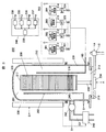
- FIG. 2 is a schematic configuration diagram of the substrate processing apparatus 101 in the embodiment of the present invention.
- the substrate processing apparatus 101 includes a gas supply system 300, a transfer machine 106, a cassette 110, a processing furnace 202, a boat 217, a controller 240, a vacuum exhaust device 246, a load lock chamber 140, and the like.
- a plurality of cassettes 110 are accommodated in the substrate processing apparatus 101, and the cassettes 110 hold the plurality of wafers 200 in a state of being aligned in a horizontal posture.
- the wafer 200 is formed in a disk shape.
- the transfer device 106 is for transferring the wafer 200 from the cassette 110 to the boat 217, or transferring the wafer 200 from the boat 217 to the cassette 110, and is configured so that the wafer 200 can be picked up. Yes. That is, the transfer device 106 can load (wafer charging) and unload (wafer discharging) the wafers 200 on the boat 217.
- the boat 217 is accommodated in the load lock chamber 140 located immediately below the processing furnace 202 before the film forming process is started.
- the side wall of the load lock chamber 140 is provided with an opening 141 and a lid that closes the opening 141, and the transfer device 106 performs wafer charging and wafer discharging through the opening 141.
- the soot treating furnace 202 includes a heater 206, an outer tube 205, and the like.
- a heater 206 is provided around the outer tube 205 so that the outer tube 205 can be heated.
- the processing furnace 202 is connected to a gas supply system 300 that supplies various processing gases and an evacuation device 246 that evacuates the inside. Details of the processing furnace 202 will be described later.
- the cocoon controller 240 controls various operations of the substrate processing apparatus 101.
- FIG. 3 is a schematic configuration diagram of the processing furnace 202 of the substrate processing apparatus 101, which is shown as a longitudinal sectional view.
- FIG. 3 is a view after the wafer 200 and the boat 217 are loaded into the processing chamber 201.
- the processing furnace 202 will be described with reference to FIG.
- the processing furnace 202 has a heater 206 as a heating mechanism.
- the heater 206 has a cylindrical shape, is composed of a heater wire and a heat insulating material provided around the heater wire, and is vertically installed by being supported by a holding body (not shown).
- An outer tube 205 is disposed inside the heater 206 concentrically with the heater 206.
- the outer tube 205 is made of a heat resistant material such as quartz (SiO 2 ) or silicon carbide (SiC).
- the outer tube 205 is formed in a cylindrical shape, and the upper end of the outer tube 205 is closed and the lower end is opened.
- a manifold 209 is provided below the outer tube 205.
- the manifold 209 is made of stainless steel or other metal material.
- the manifold 209 is provided in a cylindrical shape, and the upper end and the lower end of the manifold 209 are open.
- the diameter of the manifold 209 is equal to the diameter of the outer tube 205, the upper end of the manifold 209 is connected to the lower end of the outer tube 205, and the outer tube 205 is supported by the manifold 209.
- An O-ring as a seal member is provided between the manifold 209 and the outer tube 205. Since the manifold 209 is supported by a holding body (not shown), the outer tube 205 is installed vertically.
- a reaction vessel is formed by the outer tube 205 and the manifold 209. Then, the processing chamber 201 in the reaction container is divided into a space 212 in the outer tube 205 and a lower space 213 that is a space in the manifold 209 and below the connection portion of the outer tube 205 and the manifold 209.
- a seal cap 219 is provided as a furnace port lid capable of airtightly closing the lower end opening of the manifold 209.
- the seal cap 219 is made of stainless steel or other metal and has a disk shape.
- an O-ring as a seal member that comes into contact with the lower end of the manifold 209 is provided.
- the seal cap 219 is provided with a rotation mechanism 254.
- a rotation shaft 255 of the rotation mechanism 254 passes through the seal cap 219 and is connected to the boat 217.
- the rotation mechanism 254 is configured to rotate the wafer 200 by rotating the boat 217.
- the seal cap 219 is lifted and lowered in the vertical direction by a boat elevator 115 as a lifting mechanism provided outside the processing furnace 202. Thereby, the boat 217 can be carried into and out of the processing chamber 201.
- a drive control unit 237 is electrically connected to the rotation mechanism 254 and the boat elevator 115, and is configured to control at a desired timing so as to perform a desired operation.
- a boat 217 serving as a substrate holder is made of a heat-resistant material such as quartz or silicon carbide, and a plurality of (for example, about 50 to 150) wafers 200 are aligned in a horizontal posture with their centers aligned. It is configured to be held in multiple stages.
- a plurality of heat insulating plates 216 as disc-shaped heat insulating members made of quartz, silicon carbide or other heat-resistant materials are arranged in a multi-stage in a horizontal posture. It is configured to be difficult to be transmitted to the manifold 209 side.
- a temperature sensor 263 is provided inside the outer tube 205.
- a temperature controller 238 is electrically connected to the heater 206 and the temperature sensor 263, and the temperature in the processing chamber 201 is adjusted by adjusting the amount of current supplied to the heater 206 based on the temperature information detected by the temperature sensor 263. Is controlled at a desired timing so as to have a desired temperature distribution.
- a soot gas supply pipe 165 is provided in the manifold 209.
- the gas supply pipe 165 extends from the outside of the manifold 209 through the manifold 209 to the inside of the processing chamber 201.
- the downstream end of the gas supply pipe 165 is a nozzle.
- the downstream end of the soot gas supply pipe 165 is in the space 212.
- the upstream side of the gas supply pipe 165 is connected to valves 321 to 324.
- the valve 321 is connected to a Si-based source gas supply source 301 via an MFC (mass flow controller) 311.
- the valve 322 is connected to the Ge-based source gas supply source 302 via the MFC 312.
- the valve 323 is connected to the dilution gas supply source 303 via the MFC 313.
- the valve 324 is connected to the etching gas supply source 304 via the MFC 314.
- the Si-based source gas supply source 301 includes a monosilane gas (SiH 4 ) or a gas such as Si 2 H 6 , Si 3 H 8 , SiCl 4 , SiHCl 3 , SiH 2 Cl 2 , and Si as a constituent element. Contains gas.
- the Ge-based source gas supply source 302 is filled with a gas containing Ge as a constituent element such as monogermane gas (GeH 4 ), GeCl 4, or the like. Dilution gas such as hydrogen gas, helium gas or argon gas is sealed in the dilution gas supply source 303.
- the etching gas supply source 304 is filled with a gas such as chlorine gas or hydrogen chloride gas containing Cl as a constituent element.
- the MFCs 311 to 314 are gas flow rate control devices that detect the flow rate of the gas flowing through it and adjust the flow rate.
- a gas flow rate control unit 235 is electrically connected to the MFCs 311 to 314 and the valves 321 to 324, and is configured to control at a desired timing so that the flow rate of the supplied gas becomes a desired flow rate.
- a gas exhaust pipe 231 is provided in the soot manifold 209, and the gas exhaust pipe 231 communicates with the lower space 213.
- a pressure sensor 243 as a pressure detector and an APC valve 242 as a pressure regulator are provided on the downstream side of the gas exhaust pipe 231, and a vacuum exhaust device 246 such as a vacuum pump is connected to the downstream side thereof.
- a pressure control unit 236 is electrically connected to the pressure sensor 243 and the APC valve 242, and the opening of the APC valve 242 is adjusted based on the pressure detected by the pressure sensor 243, so that the inside of the processing chamber 201. The pressure is controlled at a desired timing so that the pressure becomes a desired pressure.
- the gas flow rate control unit 235, the pressure control unit 236, the drive control unit 237, and the temperature control unit 238 are electrically connected to a main control unit 239 that controls the entire substrate processing apparatus 101.
- an operation unit (not shown) and an input / output unit (not shown) are electrically connected to the main control unit 239.
- These gas flow rate control unit 235, pressure control unit 236, drive control unit 237, temperature control unit 238, and main control unit 239 are configured as a controller 240.
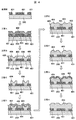
- FIG. 4 is an enlarged partial cross-sectional view of the wafer 200, and is a process diagram until the surface of the wafer 200 and the insulating film 401 are all covered with a single crystal film.
- the transfer machine 106 loads the wafers 200 from the cassettes 110 into the boat 217 (wafer charging).
- the transfer machine 106 that has delivered the wafer 200 to the boat 217 returns to the cassette 110 and loads the subsequent wafer 200 into the boat 217.
- the wafer 200 is made of single crystal silicon, and an insulating film 401 is partially formed on the surface thereof. A part of the surface of the wafer 200 is exposed between the insulating films 401, and the exposed part is a single crystal silicon portion 403.
- the controller 240 causes the drive control unit 237 to raise the boat elevator 115. Then, the boat 217 holding the wafer 200 group is loaded into the processing furnace 202 (boat loading) by the ascending operation of the boat elevator 115, and the lower end opening of the manifold 209 is closed by the seal cap 219. Then, the controller 240 causes the drive control unit 237 to stop the boat elevator 115.
- the controller 240 causes the pressure control unit 236 to operate the vacuum exhaust device 246, the vacuum exhaust device 246 performs vacuum exhaust so that the inside of the processing chamber 201 has a desired pressure (degree of vacuum).
- the pressure in the processing chamber 201 is measured by the pressure sensor 243, and the APC valve 242 is feedback-controlled by the pressure control unit 236 of the controller 240 based on the measured pressure.
- the controller 240 causes the temperature controller 238 to generate heat
- the heater 206 heats the inside of the processing chamber 201 to a desired temperature.
- the amount of current supplied to the heater 206 is feedback-controlled by the temperature control unit 238 of the controller 240 based on the temperature information detected by the temperature sensor 263 so that the inside of the processing chamber 201 becomes 530 to 580 ° C.
- the controller 240 causes the drive control unit 237 to start the rotation of the rotation mechanism 254.
- the wafer 200 is rotated by rotating the boat 217 by the rotation mechanism 254.
- the controller 240 sets the set flow rates of the MFCs 311 and 313 to a predetermined flow rate by the gas flow rate control unit 235, the valves 321 and 323 are opened. Then, the Si-based source gas and the dilution gas are introduced into the processing chamber 201 through the gas supply pipe 165, and the wafer 200 is exposed to the Si-based source gas and the dilution gas. An amorphous silicon film 402 is deposited on the surface of the wafer 200 by contacting the wafer 200 when the Si-based source gas passes through the processing chamber 201. The entire surface of the wafer 200 including the insulating film 401 is covered with an amorphous silicon film 402 (deposition process A). When a preset time has elapsed, the controller 240 closes the valves 321 and 323.
- the controller 240 sets the set temperature of the heater 206 to 500 to 700 ° C. by the temperature control unit 238, and the amount of energization to the heater 206 is feedback controlled by the temperature control unit 238 of the controller 240 based on the temperature information detected by the temperature sensor 263. Is done.
- the heating chamber 206 heats up the processing chamber 201 and heats the wafer 200 and the amorphous silicon film 402. When the amorphous silicon film 402 is heated, the amorphous silicon film 402 on the insulating film 401 is polycrystallized.
- the amorphous silicon film 402 on the single crystal silicon portion 403 is single-crystallized from a portion overlapping the single crystal silicon portion 403 using the single crystal structure (single crystal silicon portion 403) of the wafer 200 as a seed. Therefore, a single crystallized portion (hereinafter referred to as single crystallized portion) 404 extends over the insulating film 401 beyond the edge of the insulating film 401 (lateral epitaxial growth), and a polycrystallized portion (hereinafter referred to as polycrystallized). Part) 405 is formed in the central part of the insulating film 401 (heating step B). Thereby, a part of the edge portion of the insulating film 401 is covered with the single crystallized portion 404.
- single crystallized portion hereinafter referred to as single crystallized portion
- the controller 240 sets the set temperature of the heater 206 to 620 to 660 ° C.
- the controller 240 recognizes that the temperature detected by the temperature sensor 263 has reached 620 to 660 ° C.
- the set flow rate of the MFC 311 is set to 4% of the total flow rate, and the set flow rate of the MFC 314 becomes 1% of the total flow rate.
- the valves 321, 323 and 324 are opened. As a result, the Si-based source gas, the dilution gas, and the etching gas are introduced into the processing chamber 201 through the gas supply pipe 165, and the wafer 200 is exposed thereto.
- the controller 240 closes the valves 321 to 324.
- the Si-based source gas and the dilution gas are again introduced into the processing chamber 201, and the wafer 200 is exposed to the Si-based source gas and the dilution gas, so that the amorphous state is formed on the surface of the wafer 200.
- a silicon film 402 is deposited (step D).
- the second heating step when the temperature of the processing chamber 201 is set to a predetermined temperature and the wafer 200 is heated, a part of the amorphous silicon film 402 (portion on the insulating film 401) is polycrystallized and a polycrystallized portion 405 is obtained. It becomes.
- the portion of the amorphous silicon film 402 that overlaps the single crystallized portion 404 formed in the first film formation step is laterally epitaxially grown by using the single crystallized portion 404 formed in the first time as a seed to be single crystallized.
- the part 404 becomes larger. Therefore, the portion covered with the single crystallized portion 404 on the insulating film 401 is further enlarged, and almost the entire portion except the surface of the insulating film 401 is covered with the single crystallized portion 404 (step E). ).
- the temperature of the processing chamber 201 is set to a predetermined temperature, the Si-based source gas is processed at 4% of the total flow rate, the etching gas is set at 1% of the total flow rate, and the dilution gas is processed at 95% of the total flow rate.
- the wafer 200 is introduced into the chamber 201 and the wafer 200 is exposed thereto. As a result, the polycrystallized portion 405 is etched leaving the single crystallized portion 404 (step F).
- Si-based source gas and dilution gas are introduced into the processing chamber 201, and the amorphous silicon film 402 is deposited by exposing the wafer 200 thereto (Step G).
- the temperature in the processing chamber is set to a predetermined temperature and the wafer 200 is heated, whereby the amorphous silicon film 402 is single-crystallized using the single-crystallized portion 404 as a seed, and the single-crystallized portion 404 is formed. Perform lateral epitaxial growth. As a result, the entire insulating film 401 is covered with the single crystallized portion 404 (step H).
- the controller 240 stops heating by the heater 206.
- the controller 240 stops the evacuation device 246 and introduces an inert gas supplied from an inert gas supply source (not shown) into the processing chamber 201.
- an inert gas supply source not shown
- the controller 240 causes the drive control unit 237 to stop the rotation mechanism 254 and lower the boat elevator 115.
- the seal cap 219 and the boat 217 are lowered by the lowering operation of the boat elevator 115, the lower end of the manifold 209 is opened, and the boat 217 holding the wafer 200 is carried out from the processing chamber 201 to the load lock chamber 140 (boat unloading).
- the processed wafer 200 is transferred from the boat 217 to the cassette 110 through the opening 141 by the transfer device 106.
- the cassette 110 on which the processed wafer 200 is placed is taken out from the substrate processing apparatus 101 by a factory transfer apparatus (not shown).
- single crystal silicon germanium may be grown instead of single crystal silicon.
- single-crystal silicon germanium is grown by supplying a Ge-based source gas at the same time as the Si-based source gas in the film-forming process and the selective growth step, using a wafer in which the single-crystal silicon germanium part and the insulating film are exposed.
- a Ge-based source gas supply source 302 is used as a gas supply source, the supply flow rate is adjusted by the MFC 312, and a Ge-based source gas such as germane gas is introduced into the processing chamber 201 through the valve 322.
- the silicon film formation process is performed three times, the heating process is performed three times, and the selective growth process is performed twice until the insulating film 401 is completely covered with the single crystallized portion 404.
- the number of times may be less or more as long as the entire surface of the insulating film 401 is covered with the single crystallized portion 404.
- the number of times depends on the size of the device, but it is preferable to repeat the entire process about 2 to 3 times with the thickness at which the single crystallized portion 404 is formed about 1.5 ⁇ m / time. Covering the entire surface with a single crystal is a necessary technique for patterning on a further surface.
- the film forming process, the heating process, and the selective growth process may be performed separately in the reaction furnace. Separation of reactors reduces time and increases efficiency.
- the present invention it is possible to perform epitaxial selective growth in which single crystal silicon is grown and polycrystalline silicon is removed.
- the amorphous silicon film forming process can be performed at a high temperature.
- the film formation speed in the film formation process is improved. Therefore, the time required for manufacturing the semiconductor device can be shortened.
- a single crystal film can be formed with a uniform film thickness on the entire surface of the substrate by repeating each step a plurality of times, and a circuit pattern can be formed in a laminated form on the single crystal film.
- FIG. 5 is a process diagram of a three-dimensional LSI manufacturing process in which semiconductor circuit layers are stacked.
- a part of the single crystal silicon portion 423 is doped with a doping material such as a boron compound or a phosphorus compound, and the doped portion becomes a drain or source 422, and the drain 422
- a semiconductor film 425 is formed (patterned) on the portion between the source 422 and the source 422, and a metal 421 is formed (patterned) on the semiconductor film 425, the drain 422, and the source 422.
- the circuit board 420 is accommodated in the processing chamber 201. In the circuit substrate 420 shown in the process I, the metal 421 and a part of the single crystal silicon portion 423 are exposed on the surface.
- an insulating film 426 is formed so as to cover the metal 421 of the circuit board 420 (step J). At this time, part of the single crystal silicon portion 423 remains exposed without being covered with the insulating film 426. Therefore, only part of the insulating film 426 and the single crystal silicon portion 423 is exposed on the surface of the circuit board 420.
- a Si-based source gas and a dilution gas are introduced into the processing chamber 201 to expose the circuit board 420 thereto.
- an amorphous silicon film 427 is formed on the surface of the circuit board 420.
- the insulating film 426 and the single crystal silicon portion 423 are covered with the amorphous silicon film 427 (process K).
- the amorphous silicon film 427 on the insulating film 426 is polycrystallized to be a polycrystallized portion 429.
- the amorphous silicon film 427 on the single crystal silicon portion 423 is epitaxially grown in the lateral direction to become a single crystal portion 428. Therefore, the single crystallization portion 428 covers a part of the insulating film 426 and the other portion is covered by the polycrystallization portion 429 (process M).
- the processing chamber is set to a predetermined temperature, and Si-based source gas, dilution gas, and etching gas are introduced into the processing chamber 201 to expose the circuit board 420 thereto. As a result, only the polycrystallized portion 429 is etched while leaving the single crystallized portion 428 (step N).
- the inside of the processing chamber 201 is set to a predetermined temperature, and then Si-based source gas is introduced into the processing chamber 201 to form an amorphous silicon film 427.
- the amorphous silicon film 427 covers the entire surface of the circuit board 420 (process P).
- a part of the amorphous silicon film 427 is polycrystallized to be a polycrystallized portion 429.
- a part of the amorphous silicon film 427 is epitaxially grown in a lateral direction from a portion overlapping with the single crystallized portion 428 formed in the first film formation process, and becomes a single crystallized portion 428. Therefore, the range in which the single crystallized portion 428 covers the insulating film 426 is enlarged, and the polycrystallized portion 429 covers the other portions.
- the inside of the processing chamber 201 is set to a predetermined temperature, and the Si-based source gas, the dilution gas, and the etching gas are introduced into the processing chamber 201, so that the single crystallization portion 428 of the circuit board 420 remains. Only the polycrystallized portion 429 is etched (process R).
- step S After the inside of the processing chamber 201 is set to a predetermined temperature, an Si-based source gas and a dilution gas are introduced into the processing chamber 201 to form an amorphous silicon film 427 (step S).
- the amorphous silicon film 427 is all laterally epitaxially grown, and the entire insulating film 426 is covered with the single crystallized portion 428 (process T).
- a semiconductor circuit can be further patterned on the circuit substrate 420 in which the insulating film 426 is covered with the single crystal silicon film 428 as described above.
- LSIs can be integrated with higher density.
- the single crystal silicon film is grown to integrate the LSI.
- the Ge-based source gas is introduced simultaneously with the Si-based source gas.
- a germanium film may be grown.
- the film forming process is performed three times, the heating process is performed three times, and the selective growth process is performed twice.
- the number of each process is not limited to this, and the entire surface of the insulating film is formed of a single crystal silicon film. If it can be covered with, it may be less or more than this.
- a plurality of substrates are processed at once using a vertical apparatus, but one or several sheets are processed using a single wafer apparatus. The substrate can also be processed at once.
- a plurality of substrates in which the single crystal silicon part and the insulating part are exposed on the surface are held in a laminated form at a predetermined interval, and are exposed to a gas atmosphere containing Si as a constituent element, and the single crystal silicon part and the insulating part
- a film forming process for forming an amorphous silicon film on the surface After the film forming step, heating the amorphous silicon film, and heating the amorphous silicon film based on the single crystal silicon portion, After the heating step, the substrate is exposed to a mixed atmosphere of a gas containing Si as a constituent element and a gas containing Cl as a constituent element, and the single crystal on the insulating portion is left while the single crystallized portion remains.
- a selective growth step for removing a portion that has not been converted A method of manufacturing a semiconductor device is provided in which the film forming step, the heating step, and the selective growth step are repeated on the
- the film formation step, the heating step, and the selective growth step are repeated for the substrate, if the entire insulating portion is covered with single crystal silicon in the heating step, the repetition is finished.
- the ratio of the gas containing Si as the constituent element to the gas containing Cl as the constituent element is 4: 1 in the mixed atmosphere, and the temperature is 620 ° C. or more.
- the mixed atmosphere has a ratio of 4% of a gas containing Si as the constituent element, 1% of a gas containing Cl as the constituent element, and 95% of a dilution gas, and the temperature is 620 to 660. Within the range of ° C.
- the gas containing Si as the constituent element is SiH 4
- the gas containing Cl as the constituent element is Cl 2 .
- a plurality of substrates in which the single crystal silicon part and the insulating part are exposed on the surface are held in a laminated form at a predetermined interval, and are exposed to a gas atmosphere containing Si as a constituent element, and the single crystal silicon part and the insulating part
- a film forming process for forming an amorphous silicon film on the surface After the film forming step, heating the amorphous silicon film, and heating the amorphous silicon film based on the single crystal silicon portion, After the heating step, the substrate is exposed to a mixed atmosphere of a gas containing Si as a constituent element and a gas containing Cl as a constituent element, and the single crystal on the insulating portion is left while the single crystallized portion remains.
- a selective growth step for removing a portion that has not been converted A method for producing a single crystal silicon film is provided in which the film formation step, the heating step, and the selective growth step are repeated on the substrate.
- the film formation step, the heating step, and the selective growth step are repeated for the substrate, if the entire insulating portion is covered with single crystal silicon in the heating step, the repetition is finished.
- the ratio of the gas containing Si as the constituent element to the gas containing Cl as the constituent element is 4: 1 in the mixed atmosphere, and the temperature is 620 ° C. or more.
- the mixed atmosphere has a ratio of 4% of a gas containing Si as the constituent element, 1% of a gas containing Cl as the constituent element, and 95% of a dilution gas, and the temperature is 620 to 660. Within the range of ° C.
- the gas containing Si as the constituent element is SiH 4
- the gas containing Cl as the constituent element is Cl 2 .
- a plurality of substrates having a single crystal silicon germanium portion and an insulating portion exposed on the surface are held in a laminated form at a predetermined interval, and exposed to a mixed atmosphere of a gas containing Si as a constituent element and a gas containing Ge as a constituent element,
- a film forming step of forming an amorphous silicon germanium film on the single crystal silicon germanium part and the insulating part After the film forming step, heating the amorphous silicon germanium film, and heating the amorphous silicon germanium film to a single crystal based on the single crystal silicon germanium part; After the heating step, the substrate is exposed to a mixed atmosphere of a gas containing Si as a constituent element, a gas containing Ge as a constituent element and a gas containing Cl as a constituent element, and the single crystallized portion remains, And a selective growth step of removing a portion that has not been monocrystallized on the insulating portion, A method of manufacturing a semiconductor
- the film forming step, the heating step, and the selective growth step are repeated for the substrate, if the entire insulating portion is covered with single crystal silicon germanium in the heating step, the repetition is finished.
- the gas containing Si as the constituent element is SiH 4
- the gas containing Ge as the constituent element is GeH 4
- the gas containing Cl as the constituent element is Cl 2 .
- a plurality of substrates having a single crystal silicon germanium portion and an insulating portion exposed on the surface are held in a laminated form at a predetermined interval, and exposed to a mixed atmosphere of a gas containing Si as a constituent element and a gas containing Ge as a constituent element,
- a film forming step of forming an amorphous silicon germanium film on the single crystal silicon germanium part and the insulating part After the film forming step, heating the amorphous silicon germanium film, and heating the amorphous silicon germanium film to a single crystal based on the single crystal silicon germanium part; After the heating step, the substrate is exposed to a mixed atmosphere of a gas containing Si as a constituent element, a gas containing Ge as a constituent element and a gas containing Cl as a constituent element, and the single crystallized portion remains, And a selective growth step of removing a portion that has not been monocrystallized on the insulating portion,
- the film forming step, the heating step, and the selective growth step are repeated for the substrate, if the entire insulating portion is covered with single crystal silicon germanium in the heating step, the repetition is finished.
- the gas containing Si as the constituent element is SiH 4
- the gas containing Ge as the constituent element is GeH 4
- the gas containing Cl as the constituent element is Cl 2 .
- the substrate with the single crystal silicon germanium part and the insulating part exposed on the surface is exposed to a mixed atmosphere of a gas containing Si as a constituent element and a gas containing Ge as a constituent element, and the single crystal silicon germanium part and the insulating part
- a film forming process for forming an amorphous silicon germanium film on the film After the film forming step, heating the amorphous silicon germanium film, and heating the amorphous silicon germanium film to a single crystal based on the single crystal silicon germanium part; After the heating step, the substrate is exposed to a mixed atmosphere of a gas containing Si as a constituent element, a gas containing Ge as a constituent element and a gas containing Cl as a constituent element, and the single crystallized portion remains, And a selective growth step of removing a portion that has not been monocrystallized on the insulating portion,
- a method for producing a single crystal silicon germanium film is provided in which the film forming step, the heating
- the film formation step, the heating step, and the selective growth step are repeated twice or more for the substrate, if the entire insulating portion is covered with single crystal silicon germanium in the heating step, the repetition is repeated. finish.
- the gas containing Si as the constituent element is SiH 4
- the gas containing Ge as the constituent element is GeH 4
- the gas containing Cl as the constituent element is Cl 2 .
Landscapes
- Recrystallisation Techniques (AREA)
- Metal-Oxide And Bipolar Metal-Oxide Semiconductor Integrated Circuits (AREA)
- Thin Film Transistor (AREA)
Abstract
横方向固相エピタキシャル成長法において単結晶膜成膜工程に要する時間を短縮し、半導体装置の製造を短時間で行うという課題を解決するため、以下の半導体装置の製造方法を用いる。 すなわち、単結晶シリコン部403及び絶縁膜401が表面において露出したウエハ200を、構成元素としてSiを含むガスの雰囲気中に曝露し、単結晶シリコン部403及び絶縁膜401の上にアモルファスのシリコン膜402を成膜する成膜工程と、該成膜工程後に、シリコン膜402を加熱して、単結晶シリコン部403を基にしてシリコン膜402を単結晶化させる加熱工程と、該加熱工程後に、ウエハ200を構成元素としてSiを含むガス及び構成元素としてClを含むガスの混合雰囲気中に曝露し、単結晶化した部分を残留させつつ、単結晶化しなかった部分を除去する選択成長工程と、を含む半導体装置の製造方法であって、ウエハ200に対して、成膜工程、加熱工程及び選択成長工程を1回以上実施する。
Description
本発明は、半導体装置の製造方法に関する。
SOI(Silicon on Insulator)構造を用いたLSI(Large Scale Integration)等の半導体装置が盛んに研究されている。これは寄生容量の低減による動作速度の高速化や、素子間分離が簡単なため高集積化しやすい等の利点があるためである。
SOI構造を形成する方法として、SIMOX(Separation by Implanted Oxygen)に代表される表面単結晶分離法が有名である。これは表面単結晶シリコン層を保存しつつ内部に絶縁膜を形成する方法である。
ここで、SOI構造を形成する方法として、横方向固相エピタキシャル成長法が注目され始めている。これは表面の一部に絶縁膜が形成されたシリコン基板を用いて、絶縁膜上の横方向エピタキシャル成長により単結晶シリコン膜を形成する方法である。その方法としては、(1)部分的に絶縁膜を形成したシリコン基板上にアモルファスのシリコンを成膜する、(2)約500~700℃で熱処理すると、シリコン開口部(絶縁膜が形成されていない基板上のシリコン部)を種として絶縁膜上のアモルファスシリコンが単結晶化していく、(3)長時間熱処理することで絶縁膜上のアモルファスシリコンが全て単結晶化する、というものである。上記(2)の工程において、縦方向に堆積されたアモルファスシリコン膜が、基板のシリコン開口部を基に、横方向に単結晶化されていくことを、横方向固相エピタキシャル成長という。
この方法によると絶縁膜の表面全体に単結晶シリコン膜が形成するので、さらにその上にも同様の繰り返しにより3次元的に回路を集積化することが可能となり、LSI構造設計の自由度が増す利点がある。
SOI構造を形成する方法として、SIMOX(Separation by Implanted Oxygen)に代表される表面単結晶分離法が有名である。これは表面単結晶シリコン層を保存しつつ内部に絶縁膜を形成する方法である。
ここで、SOI構造を形成する方法として、横方向固相エピタキシャル成長法が注目され始めている。これは表面の一部に絶縁膜が形成されたシリコン基板を用いて、絶縁膜上の横方向エピタキシャル成長により単結晶シリコン膜を形成する方法である。その方法としては、(1)部分的に絶縁膜を形成したシリコン基板上にアモルファスのシリコンを成膜する、(2)約500~700℃で熱処理すると、シリコン開口部(絶縁膜が形成されていない基板上のシリコン部)を種として絶縁膜上のアモルファスシリコンが単結晶化していく、(3)長時間熱処理することで絶縁膜上のアモルファスシリコンが全て単結晶化する、というものである。上記(2)の工程において、縦方向に堆積されたアモルファスシリコン膜が、基板のシリコン開口部を基に、横方向に単結晶化されていくことを、横方向固相エピタキシャル成長という。
この方法によると絶縁膜の表面全体に単結晶シリコン膜が形成するので、さらにその上にも同様の繰り返しにより3次元的に回路を集積化することが可能となり、LSI構造設計の自由度が増す利点がある。
しかし上記(1)の工程を高温で行うと、アモルファスシリコン膜と絶縁膜との界面に微結晶粒が形成され、これによりアモルファスシリコンが単結晶化せず多結晶化してしまう。そこで、微結晶粒を形成させないためには上記(1)の工程を低温で行う必要があるが、低温で処理するとアモルファスシリコンの成膜速度が遅くなり、半導体装置の製造にかかる時間が長くなるという問題がある。
そこで本発明の課題は、横方向選択エピタキシャル成長法を用いて、単結晶化のための熱処理の際に多結晶となってしまった部分のみを除去し、再度アモルファスシリコン成膜及び熱処理を実施することにより基板上に形成された絶縁膜を単結晶膜により短時間で覆えるようにすることである。
以上の課題を解決するために、本発明によれば、
単結晶シリコン部及び絶縁部が表面において露出した基板を、構成元素としてSiを含むガスの雰囲気中に曝露し、前記単結晶シリコン部及び前記絶縁部の上にアモルファスのシリコン膜を成膜する成膜工程と、
前記成膜工程後に、前記アモルファスのシリコン膜を加熱して、前記単結晶シリコン部を基にして前記アモルファスのシリコン膜を単結晶化させる加熱工程と、
前記加熱工程後に、前記基板を構成元素としてSiを含むガス及び構成元素としてClを含むガスの混合雰囲気中に曝露し、前記単結晶化した部分を残留させつつ、前記絶縁部の上の単結晶化しなかった部分を除去する選択成長工程と、を含み、
前記基板に対して、前記成膜工程、前記加熱工程及び前記選択成長工程を1回以上行うようにする半導体装置の製造方法が提供される。
単結晶シリコン部及び絶縁部が表面において露出した基板を、構成元素としてSiを含むガスの雰囲気中に曝露し、前記単結晶シリコン部及び前記絶縁部の上にアモルファスのシリコン膜を成膜する成膜工程と、
前記成膜工程後に、前記アモルファスのシリコン膜を加熱して、前記単結晶シリコン部を基にして前記アモルファスのシリコン膜を単結晶化させる加熱工程と、
前記加熱工程後に、前記基板を構成元素としてSiを含むガス及び構成元素としてClを含むガスの混合雰囲気中に曝露し、前記単結晶化した部分を残留させつつ、前記絶縁部の上の単結晶化しなかった部分を除去する選択成長工程と、を含み、
前記基板に対して、前記成膜工程、前記加熱工程及び前記選択成長工程を1回以上行うようにする半導体装置の製造方法が提供される。
本発明によれば、成膜工程で微結晶粒が形成され、加熱工程で多結晶膜が成長しても、その後の選択成長工程で単結晶部以外の多結晶シリコン等を除去できる。これにより成膜工程を高温で行うことができるため成膜速度が向上し、半導体装置の製造を短時間で行うことができる。
発明者等は、減圧CVD装置を用い、基板表面に単結晶シリコンを選択成長させる方法について以下に示す特性を発見した。
単結晶シリコン部及び多結晶シリコン部が表面において露出した基板を収容した処理室を620~660℃の温度範囲に設定し、希釈ガスとともに構成元素としてSiを含むガスを全流量に対し4%、構成元素としてClを含むガスを全流量に対し1%導入することで、基板の多結晶シリコン部のみを除去することができる。多結晶シリコン部は当該温度範囲内で高温にする程エッチング量を大きくすることができ、単結晶シリコン部については当該温度範囲内において温度を高くするほど膜が厚く成長する。この性質を示したグラフを図1に示している。図1は、処理室内の温度が620,640,660℃の場合のそれぞれにおける、単結晶シリコン膜及び多結晶シリコン膜の膜厚成長速度の値をプロットした図である。また、図1は構成元素としてSiを含むガスとしてSiH4(例えば40sccm)、構成元素としてClを含むガスとしてCl2(例えば10sccm)、希釈ガスとしてH2(例えば1000sccm)を用いた場合の図である。横軸は処理室内の温度(℃)を示しており、縦軸は成長速度(任意単位)を示している。また、黒のプロットは単結晶シリコン膜の成長速度、白のプロットは多結晶シリコン膜の成長速度を示している。
処理温度が620℃であるとき、単結晶膜の成長速度の値はゼロ、多結晶膜の成長速度の値はマイナスを示している。成長速度がゼロのときは膜厚に変化がないことを示しており、成長速度の値がマイナスのときは膜がエッチングされたことを示している。処理温度が640℃であると、Si基板の単結晶シリコン部上の単結晶シリコン膜は、より厚く成長し、単結晶シリコン部以外の多結晶シリコン膜のエッチング量は、より大きくなっている。処理温度が660℃であると、単結晶シリコン膜の成長速度は更に向上し、多結晶シリコン膜のエッチング量は更に大きくなる。従って、620~660℃の温度範囲内では、多結晶シリコン膜がマイナス成長であり、設定温度が高くなるにつれて単結晶シリコン膜の成長速度が漸増するとともに多結晶シリコン膜の膜厚が漸減する。従って、この特性を利用して単結晶シリコン膜を選択成長させることができる。なお、シリコンゲルマニウムについても同様と推測される。
単結晶シリコン部及び多結晶シリコン部が表面において露出した基板を収容した処理室を620~660℃の温度範囲に設定し、希釈ガスとともに構成元素としてSiを含むガスを全流量に対し4%、構成元素としてClを含むガスを全流量に対し1%導入することで、基板の多結晶シリコン部のみを除去することができる。多結晶シリコン部は当該温度範囲内で高温にする程エッチング量を大きくすることができ、単結晶シリコン部については当該温度範囲内において温度を高くするほど膜が厚く成長する。この性質を示したグラフを図1に示している。図1は、処理室内の温度が620,640,660℃の場合のそれぞれにおける、単結晶シリコン膜及び多結晶シリコン膜の膜厚成長速度の値をプロットした図である。また、図1は構成元素としてSiを含むガスとしてSiH4(例えば40sccm)、構成元素としてClを含むガスとしてCl2(例えば10sccm)、希釈ガスとしてH2(例えば1000sccm)を用いた場合の図である。横軸は処理室内の温度(℃)を示しており、縦軸は成長速度(任意単位)を示している。また、黒のプロットは単結晶シリコン膜の成長速度、白のプロットは多結晶シリコン膜の成長速度を示している。
処理温度が620℃であるとき、単結晶膜の成長速度の値はゼロ、多結晶膜の成長速度の値はマイナスを示している。成長速度がゼロのときは膜厚に変化がないことを示しており、成長速度の値がマイナスのときは膜がエッチングされたことを示している。処理温度が640℃であると、Si基板の単結晶シリコン部上の単結晶シリコン膜は、より厚く成長し、単結晶シリコン部以外の多結晶シリコン膜のエッチング量は、より大きくなっている。処理温度が660℃であると、単結晶シリコン膜の成長速度は更に向上し、多結晶シリコン膜のエッチング量は更に大きくなる。従って、620~660℃の温度範囲内では、多結晶シリコン膜がマイナス成長であり、設定温度が高くなるにつれて単結晶シリコン膜の成長速度が漸増するとともに多結晶シリコン膜の膜厚が漸減する。従って、この特性を利用して単結晶シリコン膜を選択成長させることができる。なお、シリコンゲルマニウムについても同様と推測される。
以下、図面を参照しながら上述の特性を利用した実施形態について詳細に説明する。
<第1の実施の形態>
本発明の第1の実施の形態について説明する。
<第1の実施の形態>
本発明の第1の実施の形態について説明する。
本実施形態に係る基板処理装置は、半導体装置集積回路(IC(Integrated Circuits))等の半導体装置の製造に使用される半導体製造装置の一例として構成されているものである。下記の説明では、基板処理装置の一例として、基板に対し熱処理等を行う縦型の装置を使用した場合について述べる。
図2は、本発明の実施形態における基板処理装置101の概略構成図である。
図2に示す通り基板処理装置101は、ガス供給系300、移載機106、カセット110、処理炉202、ボート217、コントローラ240、真空排気装置246及びロードロック室140等を備える。
基板処理装置101内には複数のカセット110が収容されており、カセット110は、複数のウエハ200を水平姿勢に整列させた状態で保持している。ウエハ200は、円盤状に形成されている。
移載機106は、ウエハ200をカセット110からボート217へ移載したり、ボート217からカセット110へ移載したりするためのものであり、ウエハ200をピックアップすることができるように構成されている。即ち、移載機106はウエハ200をボート217に対し装填(ウエハチャージング)及び脱装(ウエハディスチャージング)が可能となっている。ボート217は、成膜処理開始前は処理炉202の真下に位置するロードロック室140内に収容されている。ロードロック室140の側壁には開口部141と開口部141を塞ぐ蓋が設けられ、移載機106は開口部141を介してウエハチャージング及びウエハディスチャージングを行う。
処理炉202はヒータ206及びアウターチューブ205等を有する。アウターチューブ205の周囲にヒータ206が設けられており、アウターチューブ205を加熱することができるようになっている。更に処理炉202には、各種処理ガスを供給するガス供給系300及び内部を真空排気する真空排気装置246が接続されている。処理炉202の詳細については後述する。
コントローラ240は基板処理装置101の各種動作を制御する。
図3は、基板処理装置101の処理炉202の概略構成図であり、縦断面図として示されている。なお、図3はウエハ200及びボート217が処理室201内に搬入された後の図である。図3を参照して処理炉202について説明する。
図2でも示したように、処理炉202は加熱機構としてのヒータ206を有する。ヒータ206は円筒形状であり、ヒータ素線とその周囲に設けられた断熱材より構成され、図示しない保持体に支持されることにより垂直に据え付けられている。
ヒータ206の内側には、ヒータ206と同心円状にアウターチューブ205が配設されている。アウターチューブ205は、石英(SiO2)、又は炭化シリコン(SiC)等の耐熱性材料からなる。アウターチューブ205は円筒形状に形成されており、アウターチューブ205の上端が閉塞し、下端が開口している。
アウターチューブ205の下方には、マニホールド209が設けられている。マニホールド209はステンレスその他の金属材料からなる。マニホールド209が円筒形状に設けられ、マニホールド209の上端及び下端が開口している。
マニホールド209の径がアウターチューブ205の径に等しく、マニホールド209の上端がアウターチューブ205の下端に連結され、アウターチューブ205がマニホールド209に支持されている。マニホールド209とアウターチューブ205との間にはシール部材としてのOリングが設けられている。マニホールド209が図示しない保持体に支持されることにより、アウターチューブ205は垂直に据え付けられた状態となっている。
マニホールド209の径がアウターチューブ205の径に等しく、マニホールド209の上端がアウターチューブ205の下端に連結され、アウターチューブ205がマニホールド209に支持されている。マニホールド209とアウターチューブ205との間にはシール部材としてのOリングが設けられている。マニホールド209が図示しない保持体に支持されることにより、アウターチューブ205は垂直に据え付けられた状態となっている。
アウターチューブ205とマニホールド209により反応容器が形成されている。そして、反応容器内の処理室201が、アウターチューブ205内の空間212と、マニホールド209内の空間であってアウターチューブ205とマニホールド209の接続部分よりも下側の下部空間213とに分けられる。
マニホールド209の下方には、マニホールド209の下端開口を気密に閉塞可能な炉口蓋体としてのシールキャップ219が設けられている。シールキャップ219はステンレスその他の金属からなり、円盤状に形成されている。シールキャップ219の上面には、マニホールド209の下端と当接するシール部材としてのOリングが設けられている。シールキャップ219には、回転機構254が設けられている。回転機構254の回転軸255はシールキャップ219を貫通してボート217に接続されている。回転機構254は、ボート217を回転させることでウエハ200を回転させるように構成されている。シールキャップ219は、処理炉202の外側に設けられた昇降機構としてのボートエレベータ115によって垂直方向に昇降される。これによりボート217を処理室201に対し搬入搬出することが可能となっている。回転機構254及びボートエレベータ115には、駆動制御部237が電気的に接続されており、所望の動作をするよう所望のタイミングにて制御するように構成されている。
基板保持具としてのボート217は、石英、又は炭化シリコン等の耐熱性材料からなり、複数枚(例えば50~150枚程度)のウエハ200を水平姿勢でかつ互いに中心を揃えた状態で整列させて多段に保持するように構成されている。なおボート217の下部には、石英、炭化シリコンその他の耐熱性材料からなる円板形状をした断熱部材としての断熱板216が水平姿勢で多段に複数枚配置されており、ヒータ206からの熱がマニホールド209側に伝わりにくくなるよう構成されている。
また、アウターチューブ205の内部には温度センサ263が設けられている。
ヒータ206と温度センサ263には、電気的に温度制御部238が接続されており、温度センサ263により検出された温度情報に基づきヒータ206への通電量を調整することにより処理室201内の温度が所望の温度分布となるよう所望のタイミングにて制御するように構成されている。
ヒータ206と温度センサ263には、電気的に温度制御部238が接続されており、温度センサ263により検出された温度情報に基づきヒータ206への通電量を調整することにより処理室201内の温度が所望の温度分布となるよう所望のタイミングにて制御するように構成されている。
ガス供給管165がマニホールド209に設けられている。ガス供給管165はマニホールド209の外からマニホールド209を貫通して、処理室201内まで配管されている。ガス供給管165の下流側端部がノズルになっている。
ガス供給管165の下流側端部が空間212内にある。ガス供給管165の上流側がバルブ321~324に接続されている。バルブ321はMFC(マスフローコントローラ)311を介してSi系原料ガス供給源301に接続されている。同様に、バルブ322はMFC312を介してGe系原料ガス供給源302に接続されている。バルブ323はMFC313を介して希釈ガス供給源303に接続されている。バルブ324はMFC314を介してエッチングガス供給源304に接続されている。
Si系原料ガス供給源301には、モノシランガス(SiH4)、あるいは、Si2H6、Si3H8、SiCl4、SiHCl3、SiH2Cl2等のガスであって、構成元素としてSiを含むガスが封入されている。Ge系原料ガス供給源302には、モノゲルマンガス(GeH4)、GeCl4その他の構成元素としてGeを含むガスが封入されている。希釈ガス供給源303には、水素ガス、あるいは、ヘリウムガス、アルゴンガス等の希釈ガスが封入されている。エッチングガス供給源304には、塩素ガス、あるいは、塩化水素ガス等のガスであって、構成元素としてClを含むガスが封入されている。
MFC311~314は、それに流れるガスの流量を検出するとともに、流量を調節するガス流量制御装置である。
MFC311~314及びバルブ321~324にはガス流量制御部235が電気的に接続されており、供給するガスの流量が所望の流量となるよう所望のタイミングにて制御するように構成されている。
マニホールド209にガス排気管231が設けられ、このガス排気管231が下部空間213に通じている。ガス排気管231の下流側には、圧力検出器としての圧力センサ243及び圧力調整器としてのAPCバルブ242が設けられ、その下流側には、真空ポンプ等の真空排気装置246が接続されている。圧力センサ243及びAPCバルブ242には、圧力制御部236が電気的に接続されており、圧力センサ243により検出された圧力に基づいてAPCバルブ242の開度を調節することにより、処理室201内の圧力が所望の圧力となるように所望のタイミングにて制御するよう構成されている。
ガス流量制御部235、圧力制御部236、駆動制御部237、温度制御部238は、基板処理装置101全体を制御する主制御部239に電気的に接続されている。また、主制御部239には、操作部(図示略)、入出力部(図示略)が、電気的に接続されている。これら、ガス流量制御部235、圧力制御部236、駆動制御部237、温度制御部238、主制御部239は、コントローラ240として構成されている。
次に、上記構成に係る基板処理装置101の主な動作とともに、図2~図4を参照して基板上への単結晶シリコン膜製造方法及び半導体装置の製造方法について説明する。図4はウエハ200の一部断面拡大図であり、ウエハ200の表面及び絶縁膜401が全て単結晶膜で覆われるまでの工程図である。
工場内搬送装置(図示略)によって複数のカセット110が基板処理装置101内に搬入されると、移載機106はウエハ200をカセット110からボート217に装填(ウエハチャージング)する。ボート217にウエハ200を受け渡した移載機106は、カセット110に戻り後続のウエハ200をボート217に装填する。
ウエハ200は単結晶シリコンで構成され、その表面には絶縁膜401が部分的に形成されている。絶縁膜401の間には、ウエハ200の表面の一部が露出し、その露出した部分が単結晶シリコン部403である。
ウエハ200は単結晶シリコンで構成され、その表面には絶縁膜401が部分的に形成されている。絶縁膜401の間には、ウエハ200の表面の一部が露出し、その露出した部分が単結晶シリコン部403である。
予め指定された枚数のウエハ200がボート217に装填(ウエハチャージング)されると、コントローラ240が駆動制御部237によりボートエレベータ115を上昇動作させる。そうすると、ウエハ200群を保持したボート217がボートエレベータ115の上昇動作により処理炉202内に搬入(ボートローディング)され、マニホールド209の下端の開口がシールキャップ219によって閉塞される。そして、コントローラ240が駆動制御部237によりボートエレベータ115を停止させる。
続いて、コントローラ240が圧力制御部236により真空排気装置246を動作させると、処理室201内が所望の圧力(真空度)となるように真空排気装置246によって真空排気される。この際、処理室201内の圧力は圧力センサ243で測定され、この測定された圧力に基づきAPCバルブ242がコントローラ240の圧力制御部236によりフィードバック制御される。
また、コントローラ240が温度制御部238によりヒータ206を発熱させると、処理室201内が所望の温度となるようにヒータ206によって加熱される。この際、処理室201内が530~580℃となるように温度センサ263が検出した温度情報に基づきヒータ206への通電量がコントローラ240の温度制御部238によってフィードバック制御される。
続いて、コントローラ240が駆動制御部237によって回転機構254の回転を開始させる。回転機構254により、ボート217が回転されることでウエハ200が回転される。
また、コントローラ240が温度制御部238によりヒータ206を発熱させると、処理室201内が所望の温度となるようにヒータ206によって加熱される。この際、処理室201内が530~580℃となるように温度センサ263が検出した温度情報に基づきヒータ206への通電量がコントローラ240の温度制御部238によってフィードバック制御される。
続いて、コントローラ240が駆動制御部237によって回転機構254の回転を開始させる。回転機構254により、ボート217が回転されることでウエハ200が回転される。
そして、コントローラ240がガス流量制御部235によってMFC311,313の設定流量を所定の流量に設定した後、バルブ321,323を開く。そうすると、Si系原料ガス及び希釈ガスがガス供給管165を流通して処理室201内に導入され、ウエハ200がSi系原料ガス及び希釈ガスに曝露される。Si系原料ガスが処理室201内を通過する際にウエハ200と接触することによりウエハ200の表面にアモルファスのシリコン膜402が堆積する。絶縁膜401を含むウエハ200の表面全体がアモルファスのシリコン膜402で覆われる(成膜工程A)。
予め設定された時間が経過すると、コントローラ240はバルブ321,323を閉じる。
予め設定された時間が経過すると、コントローラ240はバルブ321,323を閉じる。
コントローラ240は温度制御部238によって、ヒータ206の設定温度を500~700℃に設定し、温度センサ263が検出した温度情報に基づきヒータ206への通電量がコントローラ240の温度制御部238によってフィードバック制御される。このヒータ206の昇温処理により処理室201が加熱されるとともに、ウエハ200及びアモルファスのシリコン膜402が加熱される。アモルファスのシリコン膜402が加熱されると、絶縁膜401上のアモルファスのシリコン膜402が多結晶化する。ところが、単結晶シリコン部403上のアモルファスのシリコン膜402は、ウエハ200の単結晶構造(単結晶シリコン部403)を種として、単結晶シリコン部403に重なった部分から単結晶化していく。そのため、単結晶化した部分(以下、単結晶化部)404は絶縁膜401の縁を越えて絶縁膜401の上にも広がり(横方向エピタキシャル成長)、多結晶化した部分(以下、多結晶化部)405が絶縁膜401の中央部に形成される(加熱工程B)。
これにより、絶縁膜401の縁部分の一部が単結晶化部404で覆われる。
これにより、絶縁膜401の縁部分の一部が単結晶化部404で覆われる。
予め設定された時間が経過すると、コントローラ240はヒータ206の設定温度を620~660℃に設定する。コントローラ240が温度センサ263による検出温度が620~660℃に達したことを認識したら、MFC311の設定流量を全流量の4%となるよう設定し、MFC314の設定流量を全流量の1%となるよう設定し、MFC313の設定流量を全流量の95%となるように設定した後、バルブ321,323,324を開く。これによりSi系原料ガス、希釈ガス及びエッチングガスがガス供給管165を流通して処理室201内に導入され、ウエハ200がこれに曝露される。Si系原料ガス及びエッチングガスが処理室201内を通過する際にウエハ200の表面と接触することにより多結晶化部405がエッチングされ、単結晶化部404は残留したままである(選択成長工程C)。なお、選択成長工程において単結晶化部404が残留していれば、単結晶化部404が成長してもよい。
予め設定された時間が経過すると、コントローラ240はバルブ321~324を閉じる。
予め設定された時間が経過すると、コントローラ240はバルブ321~324を閉じる。
以後、上述の成膜工程、加熱工程、選択成長工程を繰り返し(工程D~H)、その繰り返しを絶縁膜401を含むウエハ200の表面全体が単結晶膜で覆われるまで行う(工程H)。
つまり、2回目の成膜工程において、再度Si系原料ガス及び希釈ガスを処理室201内に導入し、ウエハ200がSi系原料ガス及び希釈ガスに曝露されることでウエハ200の表面上にアモルファスのシリコン膜402が堆積する(工程D)。
2回目の加熱工程において、処理室201の温度を所定温度にし、ウエハ200を加熱すると、アモルファスのシリコン膜402の一部(絶縁膜401の上の部分)が多結晶化して多結晶化部405となる。1回目の成膜工程で形成された単結晶化部404と重なったアモルファスシリコン膜402の部分は、該1回目に成膜された単結晶化部404を種として横方向エピタキシャル成長し、単結晶化部404が大きくなる。そのため、絶縁膜401上の単結晶化部404に覆われた部分がさらに大きくなり、絶縁膜401の表面の一部分を除いてほぼ全体が単結晶化部404に覆われた状態となる(工程E)。
2回目の選択成長工程において、処理室201の温度を所定温度にするとともに、Si系原料ガスを全流量の4%、エッチングガスを全流量の1%、希釈ガスを全流量の95%として処理室201内に導入し、ウエハ200をこれに曝露する。これにより単結晶化部404を残し多結晶化部405がエッチングされる(工程F)。
3回目の成膜工程において、Si系原料ガス及び希釈ガスを処理室201内に導入し、ウエハ200をこれに曝露することでアモルファスのシリコン膜402を堆積させる(工程G)。
3回目の加熱工程において、処理室内の温度を所定の温度にし、ウエハ200を加熱することで、アモルファスのシリコン膜402が単結晶化部404を種として単結晶化され、単結晶化部404が横方向エピタキシャル成長する。これにより絶縁膜401全体が単結晶化部404によって覆われる(工程H)。
絶縁膜401の全体が単結晶化部404によって覆われたら、コントローラ240はヒータ206による加熱を停止する。またコントローラ240は真空排気装置246を停止するとともに、不活性ガス供給源(図示略)から供給される不活性ガスを処理室201内に導入する。これにより、処理室201内が不活性ガスで置換されると共に、処理室201内の圧力が常圧に復帰される。
続いて、コントローラ240が駆動制御部237により回転機構254を停止させるとともにボートエレベータ115を下降動作させる。シールキャップ219及びボート217がボートエレベータ115の下降動作により下降されて、マニホールド209の下端が開口されるとともに、ウエハ200を保持したボート217が処理室201からロードロック室140に搬出(ボートアンローディング)される。続いて移載機106により、開口部141を介して処理済ウエハ200がボート217からカセット110に移載される。処理済ウエハ200が載置されたカセット110は、工場内搬送装置(図示略)によって基板処理装置101から取り出される。
なお、本実施形態は絶縁膜401上に単結晶シリコンを成長させる方法について示しているが、単結晶シリコンでなく単結晶シリコンゲルマニウムを成長させるものとしてもよい。その場合には、単結晶シリコンゲルマニウム部及び絶縁膜が露出したウエハを用い、成膜工程及び選択成長工程において、Si系原料ガスと同時にGe系原料ガスを供給することにより単結晶シリコンゲルマニウムを成長させる。その場合には、ガス供給源としてGe系原料ガス供給源302を用い、供給流量をMFC312により調節し、バルブ322を介して処理室201内にゲルマンガス等のGe系原料ガスを導入する。
また、本実施形態では絶縁膜401を完全に単結晶化部404で覆うまでに、シリコン成膜工程を3回、加熱工程を3回、選択成長工程を2回行っているが、この回数に限らず、絶縁膜401の表面全体が単結晶化部404で覆われればこの回数より少なくてもよいし多くてもよい。この回数はデバイスのサイズにもよるが、単結晶化部404が形成される厚さが1.5μm程度/回として、全工程を2~3回程度繰り返すことが好ましい。表面全体が単結晶で覆われることはさらなる表面へのパターン形成を行うために必要な技術である。
また、本実施形態のように全ての処理を同一の処理炉で行ってもよいが、成膜工程と、加熱工程及び選択成長処理は、反応炉を分けて実施してもよい。反応炉を分けると時間短縮になり、効率が良い。
また、本実施形態では絶縁膜401を完全に単結晶化部404で覆うまでに、シリコン成膜工程を3回、加熱工程を3回、選択成長工程を2回行っているが、この回数に限らず、絶縁膜401の表面全体が単結晶化部404で覆われればこの回数より少なくてもよいし多くてもよい。この回数はデバイスのサイズにもよるが、単結晶化部404が形成される厚さが1.5μm程度/回として、全工程を2~3回程度繰り返すことが好ましい。表面全体が単結晶で覆われることはさらなる表面へのパターン形成を行うために必要な技術である。
また、本実施形態のように全ての処理を同一の処理炉で行ってもよいが、成膜工程と、加熱工程及び選択成長処理は、反応炉を分けて実施してもよい。反応炉を分けると時間短縮になり、効率が良い。
以上に示された本発明の実施形態によれば、単結晶シリコンを成長させるとともに多結晶シリコンを除去するエピタキシャル選択成長を行うことができる。これにより、成膜工程及び加熱工程において生じた多結晶シリコン部を選択成長工程により除去できるので、高温でアモルファスシリコンの成膜処理を行うことができる。成膜処理を高温で行うことで、成膜処理における成膜速度が向上する。従って、半導体装置の製造にかかる時間を短縮化することができる。
また、各工程を複数回繰り返すことで基板表面全体に均一な膜厚で単結晶膜を形成することができると考えられ、単結晶膜上に積層状に回路パターンを形成することができる。
また、各工程を複数回繰り返すことで基板表面全体に均一な膜厚で単結晶膜を形成することができると考えられ、単結晶膜上に積層状に回路パターンを形成することができる。
<第2の実施の形態>
次に、本発明の第2の実施の形態について説明する。
第2の実施形態においても第1の実施形態と同様の基板処理装置を使用する。
次に、本発明の第2の実施の形態について説明する。
第2の実施形態においても第1の実施形態と同様の基板処理装置を使用する。
図5は半導体回路層を積層していく3次元LSI製造プロセスの工程図である。
回路基板420の最上層の半導体回路層430においては、単結晶のシリコン部423の一部にホウ素化合物、又はリン化合物等のドープ材がドープされ、そのドープ部分がドレイン又はソース422となり、ドレイン422とソース422の間の部分の上に絶縁膜を介して半導体膜425が形成(パターニング)され、更に、半導体膜425及びドレイン422とソース422の上にメタル421が形成(パターニング)されている。回路基板420は処理室201内に収容される。
工程Iに示す回路基板420はメタル421及び単結晶シリコン部423の一部が表面に露出している。まず、この回路基板420のメタル421を覆うようにして絶縁膜426が形成される(工程J)。このとき単結晶シリコン部423の一部は絶縁膜426に覆われずに露出した状態のままである。従って回路基板420の表面には、絶縁膜426及び単結晶シリコン部423の一部のみが露出していることとなる。
工程Iに示す回路基板420はメタル421及び単結晶シリコン部423の一部が表面に露出している。まず、この回路基板420のメタル421を覆うようにして絶縁膜426が形成される(工程J)。このとき単結晶シリコン部423の一部は絶縁膜426に覆われずに露出した状態のままである。従って回路基板420の表面には、絶縁膜426及び単結晶シリコン部423の一部のみが露出していることとなる。
処理室201を所定温度に設定するとともに、処理室201内にSi系原料ガス及び希釈ガスを導入し、回路基板420をこれに曝露する。そうすると、回路基板420の表面にアモルファスのシリコン膜427が形成する。アモルファスのシリコン膜427によって絶縁膜426及び単結晶シリコン部423が覆われる(工程K)。
処理室201を所定温度に設定し、回路基板420を加熱処理すると、絶縁膜426上のアモルファスのシリコン膜427が多結晶化し、多結晶化部429となる。一方、単結晶シリコン部423上のアモルファスシリコン膜427は横方向エピタキシャル成長し、単結晶化部428となる。そのため、単結晶化部428は絶縁膜426の一部を覆い、それ以外の部分を多結晶化部429が覆う(工程M)。
処理室を所定の温度に設定するとともに、処理室201内にSi系原料ガス、希釈ガス及びエッチングガスを導入し、回路基板420をこれに曝露する。これにより単結晶化部428を残しつつ、多結晶化部429のみがエッチングされる(工程N)。
2回目の成膜工程において、処理室201内を所定温度に設定した上で、処理室201内にSi系原料ガスを導入し、アモルファスのシリコン膜427を形成する。アモルファスのシリコン膜427は回路基板420の表面全体を覆う(工程P)。
2回目の加熱工程において、処理室201内を所定温度に設定し、回路基板420を加熱すると、アモルファスのシリコン膜427の一部が多結晶化し多結晶化部429となる。アモルファスのシリコン膜427の一部は1回目の成膜工程で形成された単結晶化部428と重なった部分から横方向エピタキシャル成長し、単結晶化部428となる。よって単結晶化部428が絶縁膜426を覆う範囲が拡大し、それ以外の部分を多結晶化部429が覆う。(工程Q)
2回目の選択成長工程において、処理室201内を所定温度にし、処理室201内にSi系原料ガス、希釈ガス及びエッチングガスを導入することで、回路基板420の単結晶化部428を残しつつ多結晶化部429のみがエッチングされる(工程R)。
3回目の成膜工程において、処理室201内を所定温度にした上で、処理室201内にSi系原料ガス及び希釈ガスを導入し、アモルファスのシリコン膜427を形成する(工程S)。
3回目の加熱工程において、回路基板420を加熱処理するとアモルファスのシリコン膜427が全て横方向エピタキシャル成長し、絶縁膜426全体が単結晶化部428で覆われる(工程T)。
以上のようにして絶縁膜426を単結晶シリコン膜428で覆った回路基板420には、更に半導体回路をパターニングすることができる。この方法によりLSIをより高密度に集積化することが可能である。
なお、本実施形態は単結晶シリコン膜を成長させてLSIを集積化するものであったが、成膜工程及び選択成長工程において、Si系原料ガスと同時にGe系原料ガスを導入し単結晶シリコンゲルマニウム膜を成長させてもよい。
また、本実施形態では成膜工程を3回、加熱工程を3回、選択成長工程を2回行っているが、各工程の回数はこれに限られず、絶縁膜の表面全体を単結晶シリコン膜で覆うことができればこれより少なくてもよいし多くてもよい。
また、上述した第1の実施形態、第2の実施形態においては、縦型装置を用いて、複数の基板を一度に処理しているが、枚葉装置を用いて、1数ないし数枚の基板を一度に処理することもできる。
なお、本実施形態は単結晶シリコン膜を成長させてLSIを集積化するものであったが、成膜工程及び選択成長工程において、Si系原料ガスと同時にGe系原料ガスを導入し単結晶シリコンゲルマニウム膜を成長させてもよい。
また、本実施形態では成膜工程を3回、加熱工程を3回、選択成長工程を2回行っているが、各工程の回数はこれに限られず、絶縁膜の表面全体を単結晶シリコン膜で覆うことができればこれより少なくてもよいし多くてもよい。
また、上述した第1の実施形態、第2の実施形態においては、縦型装置を用いて、複数の基板を一度に処理しているが、枚葉装置を用いて、1数ないし数枚の基板を一度に処理することもできる。
以上、本発明の好ましい実施形態を説明したが、本発明の好ましい第1の態様によれば、
単結晶シリコン部及び絶縁部が表面において露出した複数の基板を所定の間隔で積層状に保持し、構成元素としてSiを含むガスの雰囲気中に曝露し、前記単結晶シリコン部及び前記絶縁部の上にアモルファスのシリコン膜を成膜する成膜工程と、
前記成膜工程後に、前記アモルファスのシリコン膜を加熱して、前記単結晶シリコン部を基にして前記アモルファスのシリコン膜を単結晶化させる加熱工程と、
前記加熱工程後に、前記基板を構成元素としてSiを含むガス及び構成元素としてClを含むガスの混合雰囲気中に曝露し、前記単結晶化した部分を残留させつつ、前記絶縁部の上の単結晶化しなかった部分を除去する選択成長工程と、を含み、
前記基板に対して、前記成膜工程、前記加熱工程及び前記選択成長工程を繰り返すようにする半導体装置の製造方法が提供される。
単結晶シリコン部及び絶縁部が表面において露出した複数の基板を所定の間隔で積層状に保持し、構成元素としてSiを含むガスの雰囲気中に曝露し、前記単結晶シリコン部及び前記絶縁部の上にアモルファスのシリコン膜を成膜する成膜工程と、
前記成膜工程後に、前記アモルファスのシリコン膜を加熱して、前記単結晶シリコン部を基にして前記アモルファスのシリコン膜を単結晶化させる加熱工程と、
前記加熱工程後に、前記基板を構成元素としてSiを含むガス及び構成元素としてClを含むガスの混合雰囲気中に曝露し、前記単結晶化した部分を残留させつつ、前記絶縁部の上の単結晶化しなかった部分を除去する選択成長工程と、を含み、
前記基板に対して、前記成膜工程、前記加熱工程及び前記選択成長工程を繰り返すようにする半導体装置の製造方法が提供される。
好ましくは、前記第1の態様において、
前記基板に対して、前記成膜工程、前記加熱工程及び前記選択成長工程を繰り返している際に、前記加熱工程において前記絶縁部全体が単結晶シリコンによって覆われたら、その繰り返しを終了する。
前記基板に対して、前記成膜工程、前記加熱工程及び前記選択成長工程を繰り返している際に、前記加熱工程において前記絶縁部全体が単結晶シリコンによって覆われたら、その繰り返しを終了する。
好ましくは、前記第1の態様において、
前記選択成長工程において、前記混合雰囲気は前記構成元素としてSiを含むガスと前記構成元素としてClを含むガスの割合が4:1であり、その温度は620℃以上である。
前記選択成長工程において、前記混合雰囲気は前記構成元素としてSiを含むガスと前記構成元素としてClを含むガスの割合が4:1であり、その温度は620℃以上である。
好ましくは、前記第1の態様において、
前記選択成長工程において、前記混合雰囲気は前記構成元素としてSiを含むガスが4%、前記構成元素としてClを含むガスが1%、希釈ガスが95%の割合であり、その温度は620~660℃の範囲内である。
前記選択成長工程において、前記混合雰囲気は前記構成元素としてSiを含むガスが4%、前記構成元素としてClを含むガスが1%、希釈ガスが95%の割合であり、その温度は620~660℃の範囲内である。
好ましくは、前記第1の態様において、
前記構成元素としてSiを含むガスはSiH4であり、前記構成元素としてClを含むガスはCl2である。
前記構成元素としてSiを含むガスはSiH4であり、前記構成元素としてClを含むガスはCl2である。
本発明の好ましい第2の態様によれば、
単結晶シリコン部及び絶縁部が表面において露出した複数の基板を所定の間隔で積層状に保持し、構成元素としてSiを含むガスの雰囲気中に曝露し、前記単結晶シリコン部及び前記絶縁部の上にアモルファスのシリコン膜を成膜する成膜工程と、
前記成膜工程後に、前記アモルファスのシリコン膜を加熱して、前記単結晶シリコン部を基にして前記アモルファスのシリコン膜を単結晶化させる加熱工程と、
前記加熱工程後に、前記基板を構成元素としてSiを含むガス及び構成元素としてClを含むガスの混合雰囲気中に曝露し、前記単結晶化した部分を残留させつつ、前記絶縁部の上の単結晶化しなかった部分を除去する選択成長工程と、を含み、
前記基板に対して、前記成膜工程、前記加熱工程及び前記選択成長工程を繰り返すようにする単結晶シリコン膜の製造方法が提供される。
単結晶シリコン部及び絶縁部が表面において露出した複数の基板を所定の間隔で積層状に保持し、構成元素としてSiを含むガスの雰囲気中に曝露し、前記単結晶シリコン部及び前記絶縁部の上にアモルファスのシリコン膜を成膜する成膜工程と、
前記成膜工程後に、前記アモルファスのシリコン膜を加熱して、前記単結晶シリコン部を基にして前記アモルファスのシリコン膜を単結晶化させる加熱工程と、
前記加熱工程後に、前記基板を構成元素としてSiを含むガス及び構成元素としてClを含むガスの混合雰囲気中に曝露し、前記単結晶化した部分を残留させつつ、前記絶縁部の上の単結晶化しなかった部分を除去する選択成長工程と、を含み、
前記基板に対して、前記成膜工程、前記加熱工程及び前記選択成長工程を繰り返すようにする単結晶シリコン膜の製造方法が提供される。
好ましくは、前記第2の態様において、
前記基板に対して、前記成膜工程、前記加熱工程及び前記選択成長工程を繰り返している際に、前記加熱工程において前記絶縁部全体が単結晶シリコンによって覆われたら、その繰り返しを終了する。
前記基板に対して、前記成膜工程、前記加熱工程及び前記選択成長工程を繰り返している際に、前記加熱工程において前記絶縁部全体が単結晶シリコンによって覆われたら、その繰り返しを終了する。
好ましくは、前記第2の態様において、
前記選択成長工程において、前記混合雰囲気は前記構成元素としてSiを含むガスと前記構成元素としてClを含むガスの割合が4:1であり、その温度は620℃以上である。
前記選択成長工程において、前記混合雰囲気は前記構成元素としてSiを含むガスと前記構成元素としてClを含むガスの割合が4:1であり、その温度は620℃以上である。
好ましくは、前記第2の態様において、
前記選択成長工程において、前記混合雰囲気は前記構成元素としてSiを含むガスが4%、前記構成元素としてClを含むガスが1%、希釈ガスが95%の割合であり、その温度は620~660℃の範囲内である。
前記選択成長工程において、前記混合雰囲気は前記構成元素としてSiを含むガスが4%、前記構成元素としてClを含むガスが1%、希釈ガスが95%の割合であり、その温度は620~660℃の範囲内である。
好ましくは、前記第2の態様において、
前記構成元素としてSiを含むガスはSiH4であり、前記構成元素としてClを含むガスはCl2である。
前記構成元素としてSiを含むガスはSiH4であり、前記構成元素としてClを含むガスはCl2である。
本発明の好ましい第3の態様によれば、
単結晶シリコンゲルマニウム部及び絶縁部が表面において露出した複数の基板を所定の間隔で積層状に保持し、構成元素としてSiを含むガス及び構成元素としてGeを含むガスの混合雰囲気中に曝露し、前記単結晶シリコンゲルマニウム部及び前記絶縁部の上にアモルファスのシリコンゲルマニウム膜を成膜する成膜工程と、
前記成膜工程後に、前記アモルファスのシリコンゲルマニウム膜を加熱して、前記単結晶シリコンゲルマニウム部を基にして前記アモルファスのシリコンゲルマニウム膜を単結晶化させる加熱工程と、
前記加熱工程後に、前記基板を構成元素としてSiを含むガス、構成元素としてGeを含むガス及び構成元素としてClを含むガスの混合雰囲気中に曝露し、前記単結晶化した部分を残留させつつ、前記絶縁部の上の単結晶化しなかった部分を除去する選択成長工程と、を含み、
前記基板に対して、前記成膜工程、前記加熱工程及び前記選択成長工程を繰り返すようにする半導体装置の製造方法が提供される。
単結晶シリコンゲルマニウム部及び絶縁部が表面において露出した複数の基板を所定の間隔で積層状に保持し、構成元素としてSiを含むガス及び構成元素としてGeを含むガスの混合雰囲気中に曝露し、前記単結晶シリコンゲルマニウム部及び前記絶縁部の上にアモルファスのシリコンゲルマニウム膜を成膜する成膜工程と、
前記成膜工程後に、前記アモルファスのシリコンゲルマニウム膜を加熱して、前記単結晶シリコンゲルマニウム部を基にして前記アモルファスのシリコンゲルマニウム膜を単結晶化させる加熱工程と、
前記加熱工程後に、前記基板を構成元素としてSiを含むガス、構成元素としてGeを含むガス及び構成元素としてClを含むガスの混合雰囲気中に曝露し、前記単結晶化した部分を残留させつつ、前記絶縁部の上の単結晶化しなかった部分を除去する選択成長工程と、を含み、
前記基板に対して、前記成膜工程、前記加熱工程及び前記選択成長工程を繰り返すようにする半導体装置の製造方法が提供される。
好ましくは、前記第3の態様において、
前記基板に対して、前記成膜工程、前記加熱工程及び前記選択成長工程を繰り返している際に、前記加熱工程において前記絶縁部全体が単結晶シリコンゲルマニウムによって覆われたら、その繰り返しを終了する。
前記基板に対して、前記成膜工程、前記加熱工程及び前記選択成長工程を繰り返している際に、前記加熱工程において前記絶縁部全体が単結晶シリコンゲルマニウムによって覆われたら、その繰り返しを終了する。
好ましくは、前記第3の態様において、
前記構成元素としてSiを含むガスはSiH4であり、前記構成元素としてGeを含むガスはGeH4であり、前記構成元素としてClを含むガスはCl2である。
前記構成元素としてSiを含むガスはSiH4であり、前記構成元素としてGeを含むガスはGeH4であり、前記構成元素としてClを含むガスはCl2である。
本発明の好ましい第4の態様によれば、
単結晶シリコンゲルマニウム部及び絶縁部が表面において露出した複数の基板を所定の間隔で積層状に保持し、構成元素としてSiを含むガス及び構成元素としてGeを含むガスの混合雰囲気中に曝露し、前記単結晶シリコンゲルマニウム部及び前記絶縁部の上にアモルファスのシリコンゲルマニウム膜を成膜する成膜工程と、
前記成膜工程後に、前記アモルファスのシリコンゲルマニウム膜を加熱して、前記単結晶シリコンゲルマニウム部を基にして前記アモルファスのシリコンゲルマニウム膜を単結晶化させる加熱工程と、
前記加熱工程後に、前記基板を構成元素としてSiを含むガス、構成元素としてGeを含むガス及び構成元素としてClを含むガスの混合雰囲気中に曝露し、前記単結晶化した部分を残留させつつ、前記絶縁部の上の単結晶化しなかった部分を除去する選択成長工程と、を含み、
前記基板に対して、前記成膜工程、前記加熱工程及び前記選択成長工程を繰り返すようにする単結晶シリコンゲルマニウム膜の製造方法が提供される。
単結晶シリコンゲルマニウム部及び絶縁部が表面において露出した複数の基板を所定の間隔で積層状に保持し、構成元素としてSiを含むガス及び構成元素としてGeを含むガスの混合雰囲気中に曝露し、前記単結晶シリコンゲルマニウム部及び前記絶縁部の上にアモルファスのシリコンゲルマニウム膜を成膜する成膜工程と、
前記成膜工程後に、前記アモルファスのシリコンゲルマニウム膜を加熱して、前記単結晶シリコンゲルマニウム部を基にして前記アモルファスのシリコンゲルマニウム膜を単結晶化させる加熱工程と、
前記加熱工程後に、前記基板を構成元素としてSiを含むガス、構成元素としてGeを含むガス及び構成元素としてClを含むガスの混合雰囲気中に曝露し、前記単結晶化した部分を残留させつつ、前記絶縁部の上の単結晶化しなかった部分を除去する選択成長工程と、を含み、
前記基板に対して、前記成膜工程、前記加熱工程及び前記選択成長工程を繰り返すようにする単結晶シリコンゲルマニウム膜の製造方法が提供される。
好ましくは、前記第4の態様において、
前記基板に対して、前記成膜工程、前記加熱工程及び前記選択成長工程を繰り返している際に、前記加熱工程において前記絶縁部全体が単結晶シリコンゲルマニウムによって覆われたら、その繰り返しを終了する。
前記基板に対して、前記成膜工程、前記加熱工程及び前記選択成長工程を繰り返している際に、前記加熱工程において前記絶縁部全体が単結晶シリコンゲルマニウムによって覆われたら、その繰り返しを終了する。
好ましくは、前記第4の態様において、
前記構成元素としてSiを含むガスはSiH4であり、前記構成元素としてGeを含むガスはGeH4であり、前記構成元素としてClを含むガスはCl2である。
前記構成元素としてSiを含むガスはSiH4であり、前記構成元素としてGeを含むガスはGeH4であり、前記構成元素としてClを含むガスはCl2である。
本発明の好ましい第5の態様によれば、
単結晶シリコンゲルマニウム部及び絶縁部が表面において露出した基板を、構成元素としてSiを含むガス及び構成元素としてGeを含むガスの混合雰囲気中に曝露し、前記単結晶シリコンゲルマニウム部及び前記絶縁部の上にアモルファスのシリコンゲルマニウム膜を成膜する成膜工程と、
前記成膜工程後に、前記アモルファスのシリコンゲルマニウム膜を加熱して、前記単結晶シリコンゲルマニウム部を基にして前記アモルファスのシリコンゲルマニウム膜を単結晶化させる加熱工程と、
前記加熱工程後に、前記基板を構成元素としてSiを含むガス、構成元素としてGeを含むガス及び構成元素としてClを含むガスの混合雰囲気中に曝露し、前記単結晶化した部分を残留させつつ、前記絶縁部の上の単結晶化しなかった部分を除去する選択成長工程と、を含み、
前記基板に対して、前記成膜工程、前記加熱工程及び前記選択成長工程を1回以上行うようにする単結晶シリコンゲルマニウム膜の製造方法が提供される。
単結晶シリコンゲルマニウム部及び絶縁部が表面において露出した基板を、構成元素としてSiを含むガス及び構成元素としてGeを含むガスの混合雰囲気中に曝露し、前記単結晶シリコンゲルマニウム部及び前記絶縁部の上にアモルファスのシリコンゲルマニウム膜を成膜する成膜工程と、
前記成膜工程後に、前記アモルファスのシリコンゲルマニウム膜を加熱して、前記単結晶シリコンゲルマニウム部を基にして前記アモルファスのシリコンゲルマニウム膜を単結晶化させる加熱工程と、
前記加熱工程後に、前記基板を構成元素としてSiを含むガス、構成元素としてGeを含むガス及び構成元素としてClを含むガスの混合雰囲気中に曝露し、前記単結晶化した部分を残留させつつ、前記絶縁部の上の単結晶化しなかった部分を除去する選択成長工程と、を含み、
前記基板に対して、前記成膜工程、前記加熱工程及び前記選択成長工程を1回以上行うようにする単結晶シリコンゲルマニウム膜の製造方法が提供される。
好ましくは、前記第5の態様において、
前記基板に対して、前記成膜工程、前記加熱工程及び前記選択成長工程を2回以上繰り返している際に、前記加熱工程において前記絶縁部全体が単結晶シリコンゲルマニウムによって覆われたら、その繰り返しを終了する。
前記基板に対して、前記成膜工程、前記加熱工程及び前記選択成長工程を2回以上繰り返している際に、前記加熱工程において前記絶縁部全体が単結晶シリコンゲルマニウムによって覆われたら、その繰り返しを終了する。
好ましくは、前記第5の態様において、
前記構成元素としてSiを含むガスはSiH4であり、前記構成元素としてGeを含むガスはGeH4であり、前記構成元素としてClを含むガスはCl2である。
前記構成元素としてSiを含むガスはSiH4であり、前記構成元素としてGeを含むガスはGeH4であり、前記構成元素としてClを含むガスはCl2である。
101・・基板処理装置、165・・ガス供給管、200・・基板、201・・処理室、205・・アウターチューブ、206・・ヒータ、240・・コントローラ、263・・温度センサ、300・・ガス供給系、301・・Si系原料ガス供給源、302・・Ge系原料ガス供給源、303・・希釈ガス供給源、304・・エッチングガス供給源、311~314・・MFC、321~324・・バルブ、401・・絶縁部、402・・シリコン膜、403・・単結晶シリコン部、404・・単結晶化部、405・・多結晶化部。
Claims (2)
- 単結晶シリコン部及び絶縁部が表面において露出した複数の基板を所定の間隔で積層状に保持し、構成元素としてSiを含むガスの雰囲気中に曝露し、前記単結晶シリコン部及び前記絶縁部の上にアモルファスのシリコン膜を成膜する成膜工程と、
前記成膜工程後に、前記シリコン膜を加熱して、前記単結晶シリコン部を基にして前記アモルファスのシリコン膜を単結晶化させる加熱工程と、
前記加熱工程後に、前記基板を構成元素としてSiを含むガス及び構成元素としてClを含むガスの混合雰囲気中に曝露し、前記単結晶化した部分を残留させつつ、前記絶縁部の上の単結晶化しなかった部分を除去する選択成長工程と、を含み、
前記基板に対して、前記成膜工程、前記加熱工程及び前記選択成長工程を繰り返すようにする半導体装置の製造方法。 - 前記選択成長工程において、前記混合雰囲気は前記構成元素としてSiを含むガスと前記構成元素としてClを含むガスの割合が4:1であり、その温度は620℃以上である請求項1に記載の半導体装置の製造方法。
Applications Claiming Priority (2)
| Application Number | Priority Date | Filing Date | Title |
|---|---|---|---|
| JP2008-315297 | 2008-12-11 | ||
| JP2008315297A JP2010141079A (ja) | 2008-12-11 | 2008-12-11 | 半導体装置の製造方法 |
Publications (1)
| Publication Number | Publication Date |
|---|---|
| WO2010067517A1 true WO2010067517A1 (ja) | 2010-06-17 |
Family
ID=42242515
Family Applications (1)
| Application Number | Title | Priority Date | Filing Date |
|---|---|---|---|
| PCT/JP2009/006013 Ceased WO2010067517A1 (ja) | 2008-12-11 | 2009-11-11 | 半導体装置の製造方法 |
Country Status (2)
| Country | Link |
|---|---|
| JP (1) | JP2010141079A (ja) |
| WO (1) | WO2010067517A1 (ja) |
Cited By (1)
| Publication number | Priority date | Publication date | Assignee | Title |
|---|---|---|---|---|
| JP2013197171A (ja) * | 2012-03-16 | 2013-09-30 | Takehide Shirato | 半導体装置及びその製造方法 |
Families Citing this family (2)
| Publication number | Priority date | Publication date | Assignee | Title |
|---|---|---|---|---|
| JP5774439B2 (ja) * | 2011-10-14 | 2015-09-09 | 株式会社日本製鋼所 | レーザ処理装置 |
| JP2013258188A (ja) * | 2012-06-11 | 2013-12-26 | Hitachi Kokusai Electric Inc | 基板処理方法と半導体装置の製造方法、および基板処理装置 |
Citations (9)
| Publication number | Priority date | Publication date | Assignee | Title |
|---|---|---|---|---|
| JPS58120595A (ja) * | 1982-01-12 | 1983-07-18 | ゼネラル・エレクトリック・カンパニイ | マスク層上に単結晶シリコン層を形成する方法 |
| JPS60152018A (ja) * | 1984-01-20 | 1985-08-10 | Agency Of Ind Science & Technol | 半導体薄膜結晶層の製造方法 |
| JPS6476718A (en) * | 1987-09-17 | 1989-03-22 | Nec Corp | Formation of thin film |
| JPH0277113A (ja) * | 1988-06-15 | 1990-03-16 | Sanyo Electric Co Ltd | Soi構造の形成方法 |
| JPH02153523A (ja) * | 1988-12-05 | 1990-06-13 | Sharp Corp | 半導体基板の形成方法 |
| JPH0582448A (ja) * | 1991-09-20 | 1993-04-02 | Nec Corp | Soiの形成方法 |
| JPH05251407A (ja) * | 1992-03-09 | 1993-09-28 | Nec Corp | 半導体装置の製造方法 |
| JPH0992621A (ja) * | 1995-09-28 | 1997-04-04 | Oki Electric Ind Co Ltd | 半導体薄膜の選択成長方法 |
| JP2008522442A (ja) * | 2004-12-01 | 2008-06-26 | アプライド マテリアルズ インコーポレイテッド | シリコンエピタキシャル膜形成時のCl2および/またはHClの使用 |
-
2008
- 2008-12-11 JP JP2008315297A patent/JP2010141079A/ja active Pending
-
2009
- 2009-11-11 WO PCT/JP2009/006013 patent/WO2010067517A1/ja not_active Ceased
Patent Citations (9)
| Publication number | Priority date | Publication date | Assignee | Title |
|---|---|---|---|---|
| JPS58120595A (ja) * | 1982-01-12 | 1983-07-18 | ゼネラル・エレクトリック・カンパニイ | マスク層上に単結晶シリコン層を形成する方法 |
| JPS60152018A (ja) * | 1984-01-20 | 1985-08-10 | Agency Of Ind Science & Technol | 半導体薄膜結晶層の製造方法 |
| JPS6476718A (en) * | 1987-09-17 | 1989-03-22 | Nec Corp | Formation of thin film |
| JPH0277113A (ja) * | 1988-06-15 | 1990-03-16 | Sanyo Electric Co Ltd | Soi構造の形成方法 |
| JPH02153523A (ja) * | 1988-12-05 | 1990-06-13 | Sharp Corp | 半導体基板の形成方法 |
| JPH0582448A (ja) * | 1991-09-20 | 1993-04-02 | Nec Corp | Soiの形成方法 |
| JPH05251407A (ja) * | 1992-03-09 | 1993-09-28 | Nec Corp | 半導体装置の製造方法 |
| JPH0992621A (ja) * | 1995-09-28 | 1997-04-04 | Oki Electric Ind Co Ltd | 半導体薄膜の選択成長方法 |
| JP2008522442A (ja) * | 2004-12-01 | 2008-06-26 | アプライド マテリアルズ インコーポレイテッド | シリコンエピタキシャル膜形成時のCl2および/またはHClの使用 |
Cited By (1)
| Publication number | Priority date | Publication date | Assignee | Title |
|---|---|---|---|---|
| JP2013197171A (ja) * | 2012-03-16 | 2013-09-30 | Takehide Shirato | 半導体装置及びその製造方法 |
Also Published As
| Publication number | Publication date |
|---|---|
| JP2010141079A (ja) | 2010-06-24 |
Similar Documents
| Publication | Publication Date | Title |
|---|---|---|
| US7851379B2 (en) | Substrate processing method and substrate processing apparatus | |
| KR102072270B1 (ko) | 오목부 내의 결정 성장 방법 및 처리 장치 | |
| US10840094B2 (en) | Method of manufacturing semiconductor device, substrate processing apparatus, and recording medium | |
| US9997354B2 (en) | Method of manufacturing semiconductor device, substrate processing apparatus, and recording medium | |
| JP5393895B2 (ja) | 半導体装置の製造方法及び基板処理装置 | |
| KR102401389B1 (ko) | 반도체 장치의 제조 방법, 기판 처리 장치 및 프로그램 | |
| CN107680898B (zh) | 半导体装置的制造方法、基板处理装置和存储介质 | |
| US10090152B2 (en) | Method of manufacturing semiconductor device, substrate processing apparatus, and recording medium | |
| US20100151682A1 (en) | Method of manufacturing semiconductor device and substrate processing apparatus | |
| US11164744B2 (en) | Method of manufacturing semiconductor device, substrate processing apparatus, and recording medium | |
| TWI839562B (zh) | 基板處理方法、基板處理裝置及電腦程式 | |
| JP2017216335A (ja) | 半導体装置の製造方法、基板処理装置、およびプログラム | |
| US10529560B2 (en) | Method of manufacturing semiconductor device, substrate processing apparatus and recording medium | |
| WO2010067517A1 (ja) | 半導体装置の製造方法 | |
| US20240222117A1 (en) | Method of processing substrate, method of manufacturing semiconductor device, substrate processing apparatus, and recording medium | |
| US20230098703A1 (en) | Method of processing substrate, method of manufacturing semiconductor device, substrate processing apparatus, and recording medium | |
| TW202347500A (zh) | 基板處理方法,半導體裝置的製造方法,程式及基板處理裝置 | |
| KR20220138808A (ko) | 실리콘막의 성막 방법 및 성막 장치 | |
| KR20220138805A (ko) | 아몰퍼스 실리콘막의 결정화 방법 및 성막 장치 |
Legal Events
| Date | Code | Title | Description |
|---|---|---|---|
| 121 | Ep: the epo has been informed by wipo that ep was designated in this application |
Ref document number: 09831625 Country of ref document: EP Kind code of ref document: A1 |
|
| NENP | Non-entry into the national phase |
Ref country code: DE |
|
| 122 | Ep: pct application non-entry in european phase |
Ref document number: 09831625 Country of ref document: EP Kind code of ref document: A1 |