WO2010062015A1 - 벤조티아다이아졸 발색부-함유 신규 유기염료 및 이의 제조방법 - Google Patents
벤조티아다이아졸 발색부-함유 신규 유기염료 및 이의 제조방법 Download PDFInfo
- Publication number
- WO2010062015A1 WO2010062015A1 PCT/KR2009/001475 KR2009001475W WO2010062015A1 WO 2010062015 A1 WO2010062015 A1 WO 2010062015A1 KR 2009001475 W KR2009001475 W KR 2009001475W WO 2010062015 A1 WO2010062015 A1 WO 2010062015A1
- Authority
- WO
- WIPO (PCT)
- Prior art keywords
- formula
- dye
- compound
- photoelectric conversion
- titanium oxide
- Prior art date
- Legal status (The legal status is an assumption and is not a legal conclusion. Google has not performed a legal analysis and makes no representation as to the accuracy of the status listed.)
- Ceased
Links
- 0 *c1c(-c(c2n[s]nc22)ccc2-c2c(*)cc[s]2)[s]cc1 Chemical compound *c1c(-c(c2n[s]nc22)ccc2-c2c(*)cc[s]2)[s]cc1 0.000 description 7
Images
Classifications
-
- C—CHEMISTRY; METALLURGY
- C09—DYES; PAINTS; POLISHES; NATURAL RESINS; ADHESIVES; COMPOSITIONS NOT OTHERWISE PROVIDED FOR; APPLICATIONS OF MATERIALS NOT OTHERWISE PROVIDED FOR
- C09B—ORGANIC DYES OR CLOSELY-RELATED COMPOUNDS FOR PRODUCING DYES, e.g. PIGMENTS; MORDANTS; LAKES
- C09B57/00—Other synthetic dyes of known constitution
- C09B57/008—Triarylamine dyes containing no other chromophores
-
- C—CHEMISTRY; METALLURGY
- C09—DYES; PAINTS; POLISHES; NATURAL RESINS; ADHESIVES; COMPOSITIONS NOT OTHERWISE PROVIDED FOR; APPLICATIONS OF MATERIALS NOT OTHERWISE PROVIDED FOR
- C09B—ORGANIC DYES OR CLOSELY-RELATED COMPOUNDS FOR PRODUCING DYES, e.g. PIGMENTS; MORDANTS; LAKES
- C09B21/00—Thiazine dyes
-
- C—CHEMISTRY; METALLURGY
- C09—DYES; PAINTS; POLISHES; NATURAL RESINS; ADHESIVES; COMPOSITIONS NOT OTHERWISE PROVIDED FOR; APPLICATIONS OF MATERIALS NOT OTHERWISE PROVIDED FOR
- C09B—ORGANIC DYES OR CLOSELY-RELATED COMPOUNDS FOR PRODUCING DYES, e.g. PIGMENTS; MORDANTS; LAKES
- C09B29/00—Monoazo dyes prepared by diazotising and coupling
- C09B29/0025—Monoazo dyes prepared by diazotising and coupling from diazotized amino heterocyclic compounds
-
- H—ELECTRICITY
- H01—ELECTRIC ELEMENTS
- H01G—CAPACITORS; CAPACITORS, RECTIFIERS, DETECTORS, SWITCHING DEVICES, LIGHT-SENSITIVE OR TEMPERATURE-SENSITIVE DEVICES OF THE ELECTROLYTIC TYPE
- H01G9/00—Electrolytic capacitors, rectifiers, detectors, switching devices, light-sensitive or temperature-sensitive devices; Processes of their manufacture
- H01G9/20—Light-sensitive devices
- H01G9/2059—Light-sensitive devices comprising an organic dye as the active light absorbing material, e.g. adsorbed on an electrode or dissolved in solution
-
- H—ELECTRICITY
- H10—SEMICONDUCTOR DEVICES; ELECTRIC SOLID-STATE DEVICES NOT OTHERWISE PROVIDED FOR
- H10K—ORGANIC ELECTRIC SOLID-STATE DEVICES
- H10K85/00—Organic materials used in the body or electrodes of devices covered by this subclass
- H10K85/60—Organic compounds having low molecular weight
- H10K85/631—Amine compounds having at least two aryl rest on at least one amine-nitrogen atom, e.g. triphenylamine
- H10K85/633—Amine compounds having at least two aryl rest on at least one amine-nitrogen atom, e.g. triphenylamine comprising polycyclic condensed aromatic hydrocarbons as substituents on the nitrogen atom
-
- H—ELECTRICITY
- H10—SEMICONDUCTOR DEVICES; ELECTRIC SOLID-STATE DEVICES NOT OTHERWISE PROVIDED FOR
- H10K—ORGANIC ELECTRIC SOLID-STATE DEVICES
- H10K85/00—Organic materials used in the body or electrodes of devices covered by this subclass
- H10K85/60—Organic compounds having low molecular weight
- H10K85/631—Amine compounds having at least two aryl rest on at least one amine-nitrogen atom, e.g. triphenylamine
- H10K85/636—Amine compounds having at least two aryl rest on at least one amine-nitrogen atom, e.g. triphenylamine comprising heteroaromatic hydrocarbons as substituents on the nitrogen atom
-
- H—ELECTRICITY
- H01—ELECTRIC ELEMENTS
- H01G—CAPACITORS; CAPACITORS, RECTIFIERS, DETECTORS, SWITCHING DEVICES, LIGHT-SENSITIVE OR TEMPERATURE-SENSITIVE DEVICES OF THE ELECTROLYTIC TYPE
- H01G9/00—Electrolytic capacitors, rectifiers, detectors, switching devices, light-sensitive or temperature-sensitive devices; Processes of their manufacture
- H01G9/20—Light-sensitive devices
- H01G9/2027—Light-sensitive devices comprising an oxide semiconductor electrode
- H01G9/2031—Light-sensitive devices comprising an oxide semiconductor electrode comprising titanium oxide, e.g. TiO2
-
- H—ELECTRICITY
- H10—SEMICONDUCTOR DEVICES; ELECTRIC SOLID-STATE DEVICES NOT OTHERWISE PROVIDED FOR
- H10K—ORGANIC ELECTRIC SOLID-STATE DEVICES
- H10K85/00—Organic materials used in the body or electrodes of devices covered by this subclass
- H10K85/60—Organic compounds having low molecular weight
- H10K85/649—Aromatic compounds comprising a hetero atom
- H10K85/655—Aromatic compounds comprising a hetero atom comprising only sulfur as heteroatom
-
- H—ELECTRICITY
- H10—SEMICONDUCTOR DEVICES; ELECTRIC SOLID-STATE DEVICES NOT OTHERWISE PROVIDED FOR
- H10K—ORGANIC ELECTRIC SOLID-STATE DEVICES
- H10K85/00—Organic materials used in the body or electrodes of devices covered by this subclass
- H10K85/60—Organic compounds having low molecular weight
- H10K85/649—Aromatic compounds comprising a hetero atom
- H10K85/657—Polycyclic condensed heteroaromatic hydrocarbons
-
- Y—GENERAL TAGGING OF NEW TECHNOLOGICAL DEVELOPMENTS; GENERAL TAGGING OF CROSS-SECTIONAL TECHNOLOGIES SPANNING OVER SEVERAL SECTIONS OF THE IPC; TECHNICAL SUBJECTS COVERED BY FORMER USPC CROSS-REFERENCE ART COLLECTIONS [XRACs] AND DIGESTS
- Y02—TECHNOLOGIES OR APPLICATIONS FOR MITIGATION OR ADAPTATION AGAINST CLIMATE CHANGE
- Y02E—REDUCTION OF GREENHOUSE GAS [GHG] EMISSIONS, RELATED TO ENERGY GENERATION, TRANSMISSION OR DISTRIBUTION
- Y02E10/00—Energy generation through renewable energy sources
- Y02E10/50—Photovoltaic [PV] energy
- Y02E10/542—Dye sensitized solar cells
-
- Y—GENERAL TAGGING OF NEW TECHNOLOGICAL DEVELOPMENTS; GENERAL TAGGING OF CROSS-SECTIONAL TECHNOLOGIES SPANNING OVER SEVERAL SECTIONS OF THE IPC; TECHNICAL SUBJECTS COVERED BY FORMER USPC CROSS-REFERENCE ART COLLECTIONS [XRACs] AND DIGESTS
- Y02—TECHNOLOGIES OR APPLICATIONS FOR MITIGATION OR ADAPTATION AGAINST CLIMATE CHANGE
- Y02E—REDUCTION OF GREENHOUSE GAS [GHG] EMISSIONS, RELATED TO ENERGY GENERATION, TRANSMISSION OR DISTRIBUTION
- Y02E10/00—Energy generation through renewable energy sources
- Y02E10/50—Photovoltaic [PV] energy
- Y02E10/549—Organic PV cells
-
- Y—GENERAL TAGGING OF NEW TECHNOLOGICAL DEVELOPMENTS; GENERAL TAGGING OF CROSS-SECTIONAL TECHNOLOGIES SPANNING OVER SEVERAL SECTIONS OF THE IPC; TECHNICAL SUBJECTS COVERED BY FORMER USPC CROSS-REFERENCE ART COLLECTIONS [XRACs] AND DIGESTS
- Y02—TECHNOLOGIES OR APPLICATIONS FOR MITIGATION OR ADAPTATION AGAINST CLIMATE CHANGE
- Y02P—CLIMATE CHANGE MITIGATION TECHNOLOGIES IN THE PRODUCTION OR PROCESSING OF GOODS
- Y02P70/00—Climate change mitigation technologies in the production process for final industrial or consumer products
- Y02P70/50—Manufacturing or production processes characterised by the final manufactured product
Definitions
- the present invention relates to a novel organic dye containing a benzothiadiazole coloring part used in a dye-sensitized solar cell (DSSC) having high photovoltaic performance and excellent stability, and a method for producing the same.
- DSSC dye-sensitized solar cell
- Dye-sensitized solar cells have the potential to replace conventional amorphous silicon solar cells because of their higher efficiency and lower manufacturing costs than conventional silicon-based solar cells. It is a photoelectrochemical solar cell whose main constituent material is a dye molecule capable of absorbing and generating electron-hole pairs, and a transition metal oxide for transferring generated electrons.
- ruthenium metal complexes As a dye used in dye-sensitized solar cells, ruthenium metal complexes having high photovoltaic conversion efficiency of 10% or more have been widely used. This ruthenium metal complex has a disadvantage of being too expensive and difficult to purify.
- metal-free organic dyes which exhibit excellent physical properties in terms of light absorption efficiency, redox reaction stability, and intramolecular charge-transfer (CT) absorption, can replace expensive ruthenium metal complexes. It has been found that it can be used as a dye for solar cells, and research on organic dyes lacking metals has been focused on.
- Organic dyes generally have a structure of electron donor-electron acceptor residues linked by ⁇ -binding units.
- amine derivatives act as electron donors
- 2-cyanoacrylic acid or rhodanine residues act as electron acceptors
- these two sites are ⁇ -binding systems such as metaine units or thiophene chains. Is connected by.
- the structural change of the amine unit which is an electron donor, results in a change in the electronic properties, for example, an absorption spectrum shifted toward blue, and by changing the ⁇ -bond length, the absorption spectrum and redox potential. Can be adjusted.
- organic dyes having high photovoltaic performance and improved stability.
- organic dyes containing a non-planar bis-dimethylfluorenylamino residue and a bithiophene or terthiophene unit in an organic skeleton have been proposed.
- the dyes have been reported to exhibit a significantly higher photovoltaic conversion efficiency of 7% when using solvent-free ionic liquid electrolytes.
- a low bandgap chromophore such as benzothiadiazole
- an object of the present invention is to provide an organic dye, which has a higher photovoltaic performance and excellent stability than a conventional metal complex dye and an organic dye, and which can greatly improve the efficiency of a solar cell, and a method of manufacturing the same.
- the present invention exhibits a significantly improved photovoltaic conversion efficiency including the dye, J sc (short circuit photocurrent density) and a dye-sensitized photoelectric conversion device excellent in the molar absorption coefficient, and a solar cell significantly improved efficiency It aims to provide.
- the present invention provides a thiophene dye represented by the structure of any one of the following formulas (1) to (3):
- R 1 is or X, Y and Z are each independently hydrogen or C 1-30 alkyl, alkoxy or heteroalkoxy;
- R 2 , R 3 , R 4 And R 5 are each independently hydrogen, halogen, amide, cyano, hydroxyl, nitro, acyl, C 1-30 Alkyl, C 1-30 Alkoxy, C 1-30 Alkylcarbonyl or C 6-20 Aryl, C 1-30 R for alkoxy 2 And R 3 , Or R 4 And R 5 Is May combine with each other to form an oxygen-containing heterocycle;
- Ar is a C 1-50 alkyl, alkoxy, halogen, amide, cyano, hydroxyl, nitro, acyl, aryl, or a C 1-50 alkyl which is unsubstituted or substituted with a heteroaryl, aryl, alkoxy, or heteroaryl;
- n is an integer from 1 to 10.
- a compound of the following formula (8) is used as stanilthiophene or 2- (3-hexylthiophen-2-yl) -4,4,5,5-tetramethyl [1,3,2] dioxaborolane and steel ( Stille) or Suzuki coupling reaction to prepare a compound of formula 9a or 9b,
- the present invention provides a dye-sensitized photoelectric conversion device comprising an oxide semiconductor fine particles carrying a compound represented by the structure of any one of formulas (1) to (3).
- the present invention provides a dye-sensitized solar cell comprising the dye-sensitized photoelectric conversion device.
- novel thiophene-based dyes of the present invention exhibit improved photovoltaic performance, namely higher molar absorption coefficient, J sc (short circuit photocurrent density), and photoelectric conversion efficiency than conventional metal complex dyes and organic dyes, and have excellent stability. The efficiency can be greatly improved.
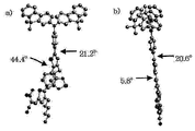
- FIG. 2 is a schematic diagram of an optimal structure calculated by TD-DFT for B3LYP / 3-21G for dyes JK-68 and JK-69 prepared in Examples 1 and 2, respectively.
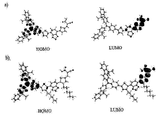
- FIG. 3 shows the geometric shapes calculated using B3LYP / 3-21G for dyes JK-68 and JK-69 prepared in Examples 1 and 2 as isodensity surface plots of HOMO and LUMO,
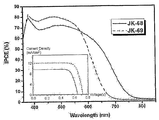
- Example 4 is a photovoltaic performance (spectrum of monochromatic incident photon-to-current conversion efficiencies (IPCEs)) and photocurrent density-voltage (J-V) curves of the DSSC prepared in Example 3;
- IPCEs monochromatic incident photon-to-current conversion efficiencies
- J-V photocurrent density-voltage
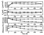
- FIG. 5 shows a short circuit photocurrent density (J SC ), an open circuit voltage (V OC ), and a fill factor measured over time while maintaining the DSSC prepared in Example 3 for 1000 hours under accelerated aging conditions. factor) and photoelectric conversion efficiency graph,
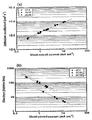
- Example 6 is a result of measuring the electron emission coefficient (a) and lifetime (b) of the DSSC prepared in Example 3 (for comparison, a dye-sensitized solar cell including a conventional dye JK-2 was prepared and compared),
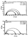
- FIG. 7 shows electrochemical impedance spectra of the DSSC prepared in Example 3 (for comparison, a dye-sensitized solar cell including the conventional dye JK-2 was prepared and compared). It is the result measured under condition (b).
- the inventors of the present invention have described the photovoltaic conversion efficiency, Jsc ( The short-circuit photocurrent density) and the molar extinction coefficient were high and the stability was confirmed to show the superior efficiency than the conventional dye-sensitized solar cell and completed the present invention.
- the organic dye of the present invention is characterized in that represented by the structure of any one of formulas (1) to (3).
- R 1 , R 2 , R 3 , R 4 , R 5 , Ar and n are as defined above, preferably R 1 is R 2 , R 3 , R 4 and R 5 are each independently hydrogen or C 4-10 alkyl, and Ar is (*: Coupling
- the compound of formula 7a or 7b is prepared by reacting with cyanoacetic acid in the presence of piperidine in chloroform.
- the present invention provides a dye-sensitized photoelectric conversion device, the dye-sensitized photoelectric conversion device is characterized in that the dye represented by the formula (1), (2) or (3) on the oxide semiconductor fine particles.
- the present invention is a dye-sensitized photoelectric conversion device in addition to using the dye represented by the formula (1), (2) or (3) method of manufacturing a dye-sensitized photoelectric conversion device for a solar cell using a conventional dye, of course,
- a thin film of an oxide semiconductor is produced on a substrate using oxide semiconductor fine particles, and then the dye of the present invention is supported on the thin film.
- the surface is electroconductive as a board
- conductive metal oxides such as tin oxide coated with indium, fluorine, and antimony on a surface of glass or a transparent polymer material such as polyethylene terephthalate or polyethersulfone, or a metal thin film such as steel, silver, or gold may be used.
- the formed thing can be used.
- the conductivity is preferably 1000 ⁇ or less, particularly preferably 100 ⁇ or less.
- a metal oxide is preferable.
- oxides such as titanium, tin, zinc, tungsten, zirconium, gallium, indium, yttrium, niobium, tantalum and vanadium can be used. Of these, oxides such as titanium, tin, zinc, niobium and indium are preferable, among these, titanium oxide, zinc oxide and tin oxide are more preferable, and titanium oxide is most preferred.
- the oxide semiconductor may be used alone, or may be mixed or coated on the surface of the semiconductor.
- the particle size of the fine particles of the oxide semiconductor is preferably 1-500 nm, more preferably 1-100 nm as the average particle diameter.
- the fine particles of the oxide semiconductor may be mixed with a large particle size and a small particle size, or may be used as a multilayer.
- the oxide semiconductor thin film is a method of forming oxide semiconductor fine particles into a thin film directly on a substrate by spray spraying, a method of electrically depositing a semiconductor fine particle thin film using a substrate as an electrode, a slurry of semiconductor fine particles or semiconductor fine particles such as a semiconductor alkoxide.
- substrate it can manufacture by the method of drying, hardening, or baking, etc.
- substrate is preferable.
- the slurry can be obtained by dispersing secondary agglomerated oxide semiconductor fine particles in a dispersion medium so as to have an average primary particle size of 1 to 200 nm.
- the dispersion medium for dispersing the slurry can be used without particular limitation so long as it can disperse the semiconductor fine particles, and alcohols such as water and ethanol, ketones such as acetone and acetylacetone, or hydrocarbons such as hexane can be used, and these can be mixed and used. Among them, it is preferable to use water among them in order to reduce the viscosity change of the slurry.
- a dispersion stabilizer can be used for the purpose of stabilizing the dispersion state of oxide semiconductor microparticles
- the substrate coated with the slurry can be fired, and its firing temperature is at least 100 ° C, preferably at least 200 ° C, and the upper limit is generally below the melting point (softening point) of the substrate, and usually the upper limit is 900 ° C, preferably 600. It is below °C.
- the firing time is not particularly limited, but is generally within 4 hours.
- substrate in this invention is 1-200 micrometers, Preferably it is 1-50 micrometers. Although some thin layers of oxide semiconductor fine particles are welded when firing, such welding is not particularly troubled for the present invention.
- the oxide semiconductor thin film may be subjected to secondary treatment.
- the performance of a semiconductor thin film may be improved by directly depositing a thin film for each substrate and drying or refiring it in a solution such as an alkoxide, chloride, nitride or sulfide of the same metal as the semiconductor.
- the metal alkoxide include titanium ethoxide, titanium isopropoxide, titanium t-butoxide, n-dibutyl-diacetyl tin and the like, and an alcohol solution thereof can be used.
- a chloride titanium tetrachloride, tin tetrachloride, zinc chloride, etc. are mentioned, for example, The aqueous solution can be used.
- the oxide semiconductor thin film thus obtained is composed of fine particles of an oxide semiconductor.
- the method of supporting the dye on the oxide semiconductor fine particles formed in the thin film phase in the present invention is not particularly limited, and as a specific example, a solution obtained by dissolving the dye represented by the formula (1), (2) or (3) as a solvent capable of dissolving the dye Or the method of immersing the board
- the concentration in the solution or dispersion can be appropriately determined by the dye.
- the deposition time is usually from room temperature to the boiling point of the solvent, and the deposition time is about 1 minute to 48 hours.
- the solvent that can be used to dissolve the dye include methanol, ethanol, acetonitrile, dimethyl sulfoxide, dimethylformamide, acetone, t-butanol and the like.
- the dye concentration of the solution is usually preferably 1 ⁇ 10 -6 M to 1 M, preferably 1 ⁇ 10 -5 M to 1 ⁇ 10 -1 M. In this way, the photoelectric conversion element of the present invention having the oxide semiconductor fine particles on the thin film sensitized with a dye can be obtained.
- the dye represented by the formula (1), (2) or (3) supported by the present invention may be one kind or may be mixed in several kinds.
- another dye or a metal complex dye can be mixed with the dye of this invention.
- metal complex dyes that can be mixed are not particularly limited, but ruthenium complexes, quaternary salts thereof, phthalocyanine, porphyrin, and the like are preferable, and organic dyes used for mixing include metal-free phthalocyanine, porphyrin, cyanine, merocyanine, Methine dyes such as oxonol, triphenylmethane, and acrylic acid dyes as shown in WO2002 / 011213, and dyes such as xanthene, azo, anthraquinone and perylene-based dyes (MK Nazeeruddin, A).
- the dyes may be adsorbed onto the semiconductor thin film in order, or may be mixed and dissolved and adsorbed.
- the dye when the dye is supported on the thin film of the oxide semiconductor fine particles, it is preferable to support the dye in the presence of the inclusion compound in order to prevent the dyes from bonding.
- the inclusion compound include deoxycholic acid, dehydrodeoxycholic acid, kenodeoxycholic acid, cholic acid methyl ester, and cholic acid such as sodium cholate, steroid-based compounds such as polyethylene oxide and cholic acid, crown ether, cyclodextrin, and calix arene, Polyethylene oxide and the like can be used.
- the semiconductor electrode surface can be treated with an amine compound such as 4-t-butyl pyridine or a compound having an acidic group such as acetic acid or propionic acid.
- an amine compound such as 4-t-butyl pyridine
- a compound having an acidic group such as acetic acid or propionic acid.
- a treatment method for example, a method of dipping a substrate provided with a thin film of semiconductor fine particles in which a dye is supported in an amine ethanol solution may be used.
- the present invention provides a dye-sensitized solar cell comprising the dye-sensitized photoelectric conversion element, the dye-sensitized photoelectric using the oxide semiconductor fine particles carrying the dye represented by the formula (1), (2) or (3)
- a conversion device conventional methods for manufacturing a solar cell using a conventional photoelectric conversion device may be applied, and, for example, the dye represented by Chemical Formula 1, Chemical Formula 2 or Chemical Formula 3 may be applied to the oxide semiconductor fine particles. It may be composed of a supported photoelectric conversion element electrode (cathode), counter electrode (anode), redox electrolyte, hole transport material or p-type semiconductor, or the like.
- one example of a specific method for manufacturing a dye-sensitized solar cell of the present invention is the step of coating a titanium oxide paste on a conductive transparent substrate, baking the substrate coated with a paste to form a titanium oxide thin film, titanium oxide thin film Impregnating the formed substrate into a mixed solution in which the dye represented by Chemical Formula 1, Chemical Formula 2 or Chemical Formula 3 is dissolved to form a titanium oxide film electrode on which the dye is adsorbed, and a second glass substrate having a counter electrode formed thereon. And forming a hole through the second glass substrate and the counter electrode, placing a thermoplastic polymer film between the counter electrode and the titanium oxide film electrode on which the dye is adsorbed, and performing a heat compression process. Bonding the counter electrode and the titanium oxide film electrode to the counter electrode and the titanium oxide film electrode through the hole. It can be prepared through the step of injecting an electrolyte into the thermoplastic polymer film and sealing the thermoplastic polymer.
- Redox electrolytes, hole transport materials, p-type semiconductors, and the like may be in the form of liquids, coagulants (gels and gels), solids, and the like.
- liquids redox electrolytes, dissolved salts, hole transport materials, p-type semiconductors, and the like are dissolved in a solvent, and at room temperature, dissolved salts, etc., in the case of coagulation bodies (gels and gels), these are polymer matrices or low molecular gelling agents. What was contained in etc. can be mentioned, respectively.
- a redox electrolyte, a dissolved salt, a hole transport material, a p-type semiconductor, or the like can be used as the solid.
- the hole transport material examples include an amine derivative, a conductive polymer such as polyacetylene, polyaniline, and polythiophene, and an object using a discotech liquid crystal phase such as triphenylene-based compound.
- a conductive polymer such as polyacetylene, polyaniline, and polythiophene
- an object using a discotech liquid crystal phase such as triphenylene-based compound.
- CuI, CuSCN, etc. can be used as a p-type semiconductor.
- the counter electrode has conductivity and catalyzes the reduction reaction of the redox electrolyte.
- platinum, carbon, rhodium, ruthenium, or the like deposited on glass or a polymer film, or coated with conductive fine particles can be used.
- a halogen redox electrolyte composed of a halogen compound having a halogen ion as a large ion and a halogen molecule, a ferrocyanate-ferrocyanate, a ferrocene-ferricinium ion, a cobalt complex and the like
- Metal redox-based electrolytes such as metal complexes, organic redox-based electrolytes such as alkylthiol-alkyldisulfides, viologen dyes, and hydroquinone-quinones, and the like, and halogen redox-based electrolytes are preferable.
- halogen molecule in the halogen redox electrolyte composed of halogen compound-halogen molecules an iodine molecule is preferable.
- a halogen compound having a halogen ion as a large ion halogenated metal salts such as LiI, NaI, KI, CaI 2 , MgI 2 and CuI, or organic ammonium salts of halogens such as tetraalkylammonium iodine, imidazolium iodine and pyridium iodine, Or I 2 can be used.
- an electrochemically inert one may be used as the solvent.
- an electrochemically inert one may be used as the solvent.
- Specific examples include acetonitrile, propylene carbonate, ethylene carbonate, 3-methoxy propionitrile, methoxy acetonitrile, ethylene glycol, propylene glycol, diethylene glycol, triethylene glycol, butyrolactone, dimethoxyethane, dimethyl carbonate, 1,3-dioxolane, methylformate, 2-methyltetrahydrofuran, 3-methoxy-oxazolidin-2-one, sulfolane, tetrahydrofuran, water, and the like, in particular acetonitrile, Propylene carbonate, ethylene carbonate, 3-methoxy propionitrile, ethylene glycol, 3-methoxy-oxazolidin-2-one, butyrolactone and the like are preferable.
- the solvents may be used alone or in combination.
- a gel positive electrolyte one containing an electrolyte or an electrolyte solution in a matrix such as an oligomer and a polymer, or one containing an electrolyte or an electrolyte solution in the same manner as a starch gelling agent can be used.
- the concentration of the redox electrolyte is preferably 0.01 to 99% by weight, more preferably 0.1 to 30% by weight.
- a counter electrode anode
- a photoelectric conversion element cathode
- a solution containing a redox electrolyte is filled therebetween.
- a solar cell was manufactured using a 10 + 4 ⁇ m TiO 2 bilayer.
- TiO 2 paste (Solaronix, Ti-Nanoxide T / SP) was screen printed on a fluorine-doped tin oxide (FTO) glass substrate to prepare a 10 ⁇ m thick first TiO 2 transparent layer, and another paste (CCIC, PST-400C) to prepare a second TiO 2 scattering layer having a thickness of 4 ⁇ m.
- FTO fluorine-doped tin oxide
- CCIC, PST-400C another paste
- This TiO 2 electrode was treated with 40 mM TiCl 4 solution at 70 ° C. for 30 minutes and sintered at 500 ° C. for 30 minutes.
- This TiO 2 electrode was then prepared using the dye compound JK-68 solution (0.3 mM dye in 10 mM kenodioxycholic acid containing tetrahydrofuran) and JK-69 solution (tetrahydro) prepared in Examples 1 and 2 above. Impregnated with 0.3 mM dye in furan) and then left at room temperature for 24 hours. A sealed sandwich cell was combined by placing a hot melt film (Surlyn) as a spacer between the dye-adsorbed TiO 2 electrode and the platinum-electrode and heating to 80 ° C.
- a hot melt film Surlyn
- DMPImI 1,2-dimethyl- n -propylimidazolium iodide
- I 2 0.1M
- NMBI 0.5M
- MPN 3-methoxypropionitrile
- PVDF-HFP poly (vinylidene fluoride- co -hexafluoro) propylene
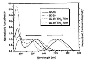
- FIG. 1 Absorption and emission spectra measured in tetrahydrofuran (THF) of the dyes JK-68 and JK-69 prepared in Examples 1 and 2 are shown in FIG. 1.
- Absorption spectra of JK-68 show two maximum absorption peaks at 534 nm and 374 nm due to the ⁇ - ⁇ transition of the conjugated system, and maximum absorption at 468 nm and 370 nm for JK-69 with hexyl groups on thiophene Show peaks.
- JK-68 shows a significant red shift, and similar red shifts are seen even when dyes JK-68 and JK-69 are adsorbed onto TiO 2 electrodes, respectively.
- FIG. 2 The optimal structures calculated by TD-DFT for B3LYP / 3-21G for dyes JK-68 and JK-69 prepared in Examples 1 and 2, respectively, are shown in FIG. 2 (a) JK-69 and b) JK -68).
- the ground state structure of JK-68 has a 20.6 degree twist between N, N -bis (9,9-dimethylfluoren-2-yl) aniline and thienyl units, thienyl and benzothiadiazole There is a backside angle of 5.8 degrees between the units.
- JK-69 has a twist angle of 21.2 degrees and 44.4 degrees, respectively.
- DMPImI 1,2-dimethyl- n -propylimidazolium iodide
- MPN 3-methoxypropionitrile
- PVDF-HFP poly (vinylidenefluoride- co -hexafluoro) propylene
- the 6.61% photoelectric conversion efficiency of JK-69 is much higher than the 6.1% reported so far.
- the high photoelectric conversion efficiency and high open circuit voltage of JK-69 are due to the introduction of substituted hexyl groups in thiophene units. will be.
- the electron emission coefficient (a) and the lifetime (b) of the DSSC prepared in Example 3 were measured and shown in FIG. 6. It was.
- Example 3 the electrochemical impedance spectrum of the DSSC prepared in Example 3 (for comparison, a dye-sensitized solar cell including the conventional dye JK-2 was prepared and compared) was also subjected to bright conditions (lighting 100 mWcm -2). It is shown in Figure 7 measured under (a) and dark conditions (b).
- the novel dye of the present invention containing a low bandgap coloring part shows excellent molar absorption coefficient, J sc (short circuit photocurrent density), photoelectric conversion efficiency and stability, thereby greatly improving the efficiency of the solar cell.
- J sc short circuit photocurrent density
- photoelectric conversion efficiency and stability thereby greatly improving the efficiency of the solar cell.
- solar cells based on JK-69 exhibit remarkably good photoelectric conversion efficiency and stability.
- novel thiophene-based dyes of the present invention exhibit improved photovoltaic performance, namely higher molar absorption coefficient, J sc (short circuit photocurrent density), and photoelectric conversion efficiency than conventional metal complex dyes and organic dyes, and have excellent stability. The efficiency can be greatly improved.
Landscapes
- Chemical & Material Sciences (AREA)
- Engineering & Computer Science (AREA)
- Organic Chemistry (AREA)
- Materials Engineering (AREA)
- Power Engineering (AREA)
- Physics & Mathematics (AREA)
- Spectroscopy & Molecular Physics (AREA)
- Microelectronics & Electronic Packaging (AREA)
- Hybrid Cells (AREA)
- Photovoltaic Devices (AREA)
- Plural Heterocyclic Compounds (AREA)
Abstract
Description


| 염료 | λabs a/nm(ε/M-1cm-1) | EOX b/V | E0-0 c/V | ELUMO d/V | JSC/mAcm-2 | VOC/V | FF | ηe(%) |
| JK-68 | 534(19 740);374(36 690) | 0.98 | 1.93 | -0.95 | 9.58 | 0.643 | 75.54 | 4.66 |
| JK-69 | 468(19 290);370(72 000) | 1.08 | 2.07 | -0.99 | 12.03 | 0.720 | 76.19 | 6.61 |
| a: 에탄올 용액 중에서 측정한 흡광 스펙트럼b: 0.1M (n-C4H9)4NPF6과 함께 CH3CN 중에서 측정한 (50 mVs-1의 스캔 속도) TiO2 상에 담지된 염료의 NHE(일반 수소 전극) 대비 산화 포텐셜c: 에탄올 중에서의 흡광 스펙트럼과 발광 스펙트럼의 교차점d: E OX - E 0-0 으로부터 산출된 값e: 0.18 cm2 작업면적 에 대해서 측정된 DSSC의 성능 | ||||||||
Claims (11)
- 하기 화학식 1 내지 3 중 어느 하나의 구조로 표시되는 티오펜계 염료:[화학식 1]
 [화학식 2]
 [화학식 3]
 상기 식에서,R1은또는
 이고, 상기 X, Y 및 Z는 각각 독립적으로 수소 또는 C1-30의 알킬, 알콕시 또는 헤테로알콕시이고;
 R2, R3, R4 및 R5는 각각 독립적으로 수소, 할로겐, 아미드, 시아노, 하이드록실, 니트로, 아실, C1-30 알킬, C1-30 알콕시, C1-30 알킬카보닐 또는 C6-20 아릴이며, C1-30 알콕시인 경우 R2와 R3, 또는 R4와 R5는 서로 결합하여 산소-함유 헤테로환을 형성할 수 있고;Ar은 C1-50의 알킬, 알콕시, 할로겐, 아미드, 시아노, 하이드록실, 니트로, 아실, 아릴 또는 헤테로아릴기로 치환되거나 치환되지 않은 C1-50의 알킬, 아릴, 알콕시 또는 헤테로아릴이며;n은 1 내지 10의 정수이다.
 - 제1항에 있어서,상기 R1이이고, R2, R3, R4 및 R5가 각각 독립적으로 수소 또는 C4-10 알킬이고, Ar이
 이고, n이 1인 것을 특징으로 하는 티오펜계 염료.
- 제1항에 있어서,상기 염료가 하기 화학식 1a 또는 1b의 화합물인 것을 특징으로 하는, 티오펜계 염료:[화학식 1a]
 [화학식 1b]
- (1) 하기 화학식 8의 화합물을 스타닐티오펜 또는 2-(3-헥실티오펜-2-일)-4,4,5,5-테트라메틸[1,3,2]다이옥사보롤란과 스틸(Stille) 또는 스즈끼(Suzuki) 커플링 반응시켜 하기 화학식 9a 또는 9b의 화합물을 제조하고,(2) 화학식 9a 또는 9b의 화합물을 유기용매 중에서 N-브로모숙신이미드와 반응시켜 브롬화하여 하기 화학식 4a 또는 4b의 화합물을 제조하고,(3) 화학식 4a 또는 4b의 화합물을 하기 화학식 5의 화합물과 스즈끼 커플링 반응시켜 하기 화학식 6a 또는 6b의 화합물을 제조하고,(4) 화학식 6a 또는 6b의 화합물을 빌스마이어-헤크(Vilsmeier-Haack) 반응에 의해 알데하이드화하여 하기 화학식 7a 또는 7b의 화합물을 제조하고,(5) 화학식 7a 또는 7b의 화합물을 클로로포름 중에서 피페리딘 존재 하에서 시아노아세트산과 반응시키는 것을 포함하는화학식 1a 또는 1b로 표시되는 염료의 제조방법:[화학식 8]
 [화학식 9a](R = H)
 [화학식 9b](R = 헥실)
 [화학식 4a](R = H)
 [화학식 4b](R = 헥실)
 [화학식 5]
 [화학식 6a](R = H)
 [화학식 6b](R = 헥실)
 [화학식 7a](R = H)
 [화학식 7b](R = 헥실)
 [화학식 1a](R = H)
 [화학식 1b](R = 헥실)
- 제4항에 있어서,상기 단계 (2)에 사용되는 유기용매가 아세트산과 다이클로로메틸의 혼합물인 것을 특징으로 하는 염료의 제조방법.
- 제1항의 티오펜계 염료를 담지시킨 산화물 반도체 미립자를 포함하는 것을 특징으로 하는 염료증감 광전변환소자.
- 제6항에 있어서,포섭화합물의 존재 하에서, 상기 산화물 반도체 미립자에 티오펜계 염료를 담지시킨 것을 특징으로 하는 염료증감 광전변환소자.
- 제7항에 있어서,상기 산화물 반도체 미립자가 이산화티탄을 필수성분으로 포함하는 것을 특징으로 하는 염료증감 광전변환소자.
- 제7항에 있어서,상기 산화물 반도체 미립자가 평균 입경이 1 - 500 nm인 것을 특징으로 하는 염료증감 광전변환소자.
- 제6항의 염료증감 광전변환소자를 전극으로서 포함하는 것을 특징으로 하는 염료감응태양전지.
- 제10항에 있어서,상기 염료감응태양전지가, 전도성 투명 기판 위에 산화티타늄 페이스트를 코팅하는 단계, 페이스트가 코팅된 기판을 소성하여 산화티타늄 박막을 형성하는 단계, 산화티타늄 박막이 형성된 기판을 화학식 1, 화학식 2 또는 화학식 3으로 표시되는 염료가 용해된 혼합용액에 함침시켜 염료가 흡착된 산화티타늄 필름 전극을 형성하는 단계, 그 상부에 대전극이 형성된 제2의 유리기판을 구비하는 단계, 제2 유리기판 및 대전극을 관통하는 홀(hole)을 형성하는 단계, 상기 대전극 및 상기 염료가 흡착된 산화티타늄 필름 전극 사이에 열가소성 고분자 필름을 두고, 가열 압착 공정을 실시하여 상기 대전극 및 산화티타늄 필름 전극을 접합시키는 단계, 상기 홀을 통하여 대전극과 산화티타늄 필름 전극 사이의 열가소성 고분자 필름에 전해질을 주입하는 단계, 및 상기 열가소성 고분자를 실링하는 단계를 통하여 제조되는 것을 특징으로 하는 염료감응태양전지.
Priority Applications (2)
| Application Number | Priority Date | Filing Date | Title |
|---|---|---|---|
| JP2011538539A JP2012509978A (ja) | 2008-11-25 | 2009-03-23 | 新規なベンゾチアジアゾール発色団含有有機染料及びその製造方法 |
| CN2009801473160A CN102245710B (zh) | 2008-11-25 | 2009-03-23 | 含有苯并噻二唑发色团的新型有机染料及其制造方法 |
Applications Claiming Priority (2)
| Application Number | Priority Date | Filing Date | Title |
|---|---|---|---|
| KR1020080117485A KR101250403B1 (ko) | 2008-11-25 | 2008-11-25 | 벤조티아다이아졸 발색부-함유 신규 유기염료 및 이의 제조방법 |
| KR10-2008-0117485 | 2008-11-25 |
Publications (1)
| Publication Number | Publication Date |
|---|---|
| WO2010062015A1 true WO2010062015A1 (ko) | 2010-06-03 |
Family
ID=42225866
Family Applications (1)
| Application Number | Title | Priority Date | Filing Date |
|---|---|---|---|
| PCT/KR2009/001475 Ceased WO2010062015A1 (ko) | 2008-11-25 | 2009-03-23 | 벤조티아다이아졸 발색부-함유 신규 유기염료 및 이의 제조방법 |
Country Status (5)
| Country | Link |
|---|---|
| JP (1) | JP2012509978A (ko) |
| KR (1) | KR101250403B1 (ko) |
| CN (1) | CN102245710B (ko) |
| TW (1) | TWI483998B (ko) |
| WO (1) | WO2010062015A1 (ko) |
Cited By (4)
| Publication number | Priority date | Publication date | Assignee | Title |
|---|---|---|---|---|
| CN101864187A (zh) * | 2010-06-11 | 2010-10-20 | 北京大学 | 一种低能级差染料、中间体及其制备方法和应用 |
| WO2013008889A1 (ja) * | 2011-07-14 | 2013-01-17 | 積水化学工業株式会社 | 光電変換素子用材料、光電変換素子の製造方法及び光電変換素子 |
| CN103880834A (zh) * | 2014-03-05 | 2014-06-25 | 南京邮电大学 | 一种有机太阳能电池材料及其制备方法 |
| ITMI20131324A1 (it) * | 2013-08-02 | 2015-02-03 | Eni Spa | Cella solare sensibilizzata da "quantum dot" e colorante |
Families Citing this family (6)
| Publication number | Priority date | Publication date | Assignee | Title |
|---|---|---|---|---|
| WO2013085285A1 (ko) * | 2011-12-05 | 2013-06-13 | 고려대학교 산학협력단 | 정공전도특성을 갖는 염료감응 태양전지용 공흡착체 및 그를 포함하는 염료감응 태양전지 |
| CN103408963B (zh) * | 2013-08-08 | 2014-08-27 | 陕西师范大学 | 脲供体双桥链有机染料及其应用 |
| CN103834190B (zh) * | 2013-12-09 | 2015-07-22 | 中国科学院长春应用化学研究所 | 含苯并噻二唑-氰基苯丙烯酸受体的有机染料及在染料敏化太阳电池中的应用 |
| CN106459608A (zh) | 2014-08-02 | 2017-02-22 | 株式会社Lg化学 | 染料复合物、光转换膜和包括其的电子装置 |
| JP2019087662A (ja) * | 2017-11-08 | 2019-06-06 | 国立大学法人山口大学 | 交互累積型オリゴマー及びその製造方法 |
| CN111704628B (zh) * | 2020-07-29 | 2022-07-29 | 湘潭大学 | 四种D-(A’-π-A)2型亚胺衍生物合金属配合物染料敏化剂及其制备方法与用途 |
Citations (4)
| Publication number | Priority date | Publication date | Assignee | Title |
|---|---|---|---|---|
| US4017313A (en) * | 1974-09-30 | 1977-04-12 | E. I. Du Pont De Nemours And Company | Photosensitive composition containing a leuco dye, a photosensitizer, an aromatic aldehyde and a secondary or tertiary amine and the use thereof in a direct-print process |
| US6353083B1 (en) * | 1999-02-04 | 2002-03-05 | The Dow Chemical Company | Fluorene copolymers and devices made therefrom |
| US20040229925A1 (en) * | 2003-05-16 | 2004-11-18 | Chunming Zhang | Process for preparing a 4,7-bis(5-halothien-2-yl)-2,1,3-benzothiadiazole and a precursor therefor |
| KR20080018238A (ko) * | 2008-02-05 | 2008-02-27 | 계광열 | 쿠마린 함유 염료 감응 태양전지용 염료 |
Family Cites Families (6)
| Publication number | Priority date | Publication date | Assignee | Title |
|---|---|---|---|---|
| DE10229370A1 (de) * | 2002-06-29 | 2004-01-15 | Covion Organic Semiconductors Gmbh | 2,1,3-Benzothiadiazole |
| US7446207B2 (en) * | 2005-09-27 | 2008-11-04 | Ctci Foundation | Organic dye used in dye-sensitized solar cell |
| KR101317533B1 (ko) * | 2006-03-02 | 2013-10-15 | 니폰 가야꾸 가부시끼가이샤 | 색소 증감 광전변환소자 |
| KR101472308B1 (ko) * | 2007-02-21 | 2014-12-15 | 주식회사 동진쎄미켐 | 신규한 루테늄계 염료 및 이의 제조방법 |
| CN101240117B (zh) * | 2008-02-04 | 2010-11-10 | 中国科学院长春应用化学研究所 | 纯有机染料和由其制备的染料敏化太阳能电池 |
| CN101265365B (zh) * | 2008-04-30 | 2010-06-09 | 天津理工大学 | 米氏酮-氰基类有机染料及其合成方法 |
-
2008
- 2008-11-25 KR KR1020080117485A patent/KR101250403B1/ko not_active Expired - Fee Related
-
2009
- 2009-03-23 CN CN2009801473160A patent/CN102245710B/zh not_active Expired - Fee Related
- 2009-03-23 WO PCT/KR2009/001475 patent/WO2010062015A1/ko not_active Ceased
- 2009-03-23 JP JP2011538539A patent/JP2012509978A/ja active Pending
- 2009-03-25 TW TW098109723A patent/TWI483998B/zh not_active IP Right Cessation
Patent Citations (4)
| Publication number | Priority date | Publication date | Assignee | Title |
|---|---|---|---|---|
| US4017313A (en) * | 1974-09-30 | 1977-04-12 | E. I. Du Pont De Nemours And Company | Photosensitive composition containing a leuco dye, a photosensitizer, an aromatic aldehyde and a secondary or tertiary amine and the use thereof in a direct-print process |
| US6353083B1 (en) * | 1999-02-04 | 2002-03-05 | The Dow Chemical Company | Fluorene copolymers and devices made therefrom |
| US20040229925A1 (en) * | 2003-05-16 | 2004-11-18 | Chunming Zhang | Process for preparing a 4,7-bis(5-halothien-2-yl)-2,1,3-benzothiadiazole and a precursor therefor |
| KR20080018238A (ko) * | 2008-02-05 | 2008-02-27 | 계광열 | 쿠마린 함유 염료 감응 태양전지용 염료 |
Cited By (7)
| Publication number | Priority date | Publication date | Assignee | Title |
|---|---|---|---|---|
| CN101864187A (zh) * | 2010-06-11 | 2010-10-20 | 北京大学 | 一种低能级差染料、中间体及其制备方法和应用 |
| CN101864187B (zh) * | 2010-06-11 | 2013-04-10 | 北京大学 | 一种低能级差染料、中间体及其制备方法和应用 |
| WO2013008889A1 (ja) * | 2011-07-14 | 2013-01-17 | 積水化学工業株式会社 | 光電変換素子用材料、光電変換素子の製造方法及び光電変換素子 |
| JP5369238B2 (ja) * | 2011-07-14 | 2013-12-18 | 積水化学工業株式会社 | 光電変換素子用材料、光電変換素子の製造方法及び光電変換素子 |
| ITMI20131324A1 (it) * | 2013-08-02 | 2015-02-03 | Eni Spa | Cella solare sensibilizzata da "quantum dot" e colorante |
| WO2015015377A1 (en) * | 2013-08-02 | 2015-02-05 | Eni S.P.A. | Quantum dot dye-sensitized solar cell |
| CN103880834A (zh) * | 2014-03-05 | 2014-06-25 | 南京邮电大学 | 一种有机太阳能电池材料及其制备方法 |
Also Published As
| Publication number | Publication date |
|---|---|
| KR20100058902A (ko) | 2010-06-04 |
| TWI483998B (zh) | 2015-05-11 |
| CN102245710A (zh) | 2011-11-16 |
| CN102245710B (zh) | 2013-11-27 |
| KR101250403B1 (ko) | 2013-04-05 |
| JP2012509978A (ja) | 2012-04-26 |
| TW201020294A (en) | 2010-06-01 |
Similar Documents
| Publication | Publication Date | Title |
|---|---|---|
| KR101330601B1 (ko) | 신규한 티오펜계 염료 및 이의 제조방법 | |
| Kim et al. | A polymer gel electrolyte to achieve≥ 6% power conversion efficiency with a novel organic dye incorporating a low-band-gap chromophore | |
| KR101250403B1 (ko) | 벤조티아다이아졸 발색부-함유 신규 유기염료 및 이의 제조방법 | |
| KR100969675B1 (ko) | 신규한 엔-아릴카바졸 잔기-함유 유기염료 및 이의제조방법 | |
| KR101008226B1 (ko) | 신규한 유기염료 및 이의 제조방법 | |
| KR101320999B1 (ko) | 신규한 유기염료 및 이의 제조방법 | |
| KR20100136929A (ko) | 신규한 유기염료 및 이의 제조방법 | |
| KR20070061810A (ko) | 색소증감 광전 변환 소자 | |
| WO2013085285A1 (ko) | 정공전도특성을 갖는 염료감응 태양전지용 공흡착체 및 그를 포함하는 염료감응 태양전지 | |
| KR20080104136A (ko) | 색소 증감 광전변환소자 | |
| Knyazeva et al. | Dye-sensitized solar cells: Investigation of DA-π-A organic sensitizers based on [1, 2, 5] selenadiazolo [3, 4-c] pyridine | |
| KR20090071426A (ko) | 신규한 루테늄계 염료 및 이의 제조방법 | |
| KR20100136931A (ko) | 신규한 유기염료 및 이의 제조방법 | |
| WO2010067996A2 (ko) | 트리알콕시실릴기 함유 신규 유기염료 및 이의 제조방법 | |
| WO2010147427A2 (ko) | 신규한 유기염료 및 이의 제조방법 | |
| WO2009096702A9 (ko) | 신규한 유기 염료 및 이의 제조방법 | |
| KR20100128094A (ko) | 신규한 줄로리딘계 염료 및 이의 제조방법 | |
| KR20100128258A (ko) | 신규한 루테늄계 염료 및 이의 제조방법 | |
| WO2009099302A2 (ko) | 염료 감응 태양전지용 염료 및 이를 함유하는 태양전지 | |
| KR20100128255A (ko) | 신규한 스파이로바이플루오렌계 염료 및 이의 제조방법 | |
| KR101173658B1 (ko) | 염료감응 태양전지용 스쿠아레인계 염료 | |
| KR101940491B1 (ko) | 신규한 루테늄계 염료 및 이의 제조방법 | |
| WO2012060587A2 (ko) | 신규한 루테늄계 염료 및 이의 제조방법 | |
| KR101633150B1 (ko) | 플루오렌 유도체 및 그의 염 | |
| WO2012057472A2 (ko) | 광전극의 제조방법 및 이에 의하여 제조한 광전극을 포함하는 태양전지 |
Legal Events
| Date | Code | Title | Description |
|---|---|---|---|
| WWE | Wipo information: entry into national phase |
Ref document number: 200980147316.0 Country of ref document: CN |
|
| 121 | Ep: the epo has been informed by wipo that ep was designated in this application |
Ref document number: 09829222 Country of ref document: EP Kind code of ref document: A1 |
|
| NENP | Non-entry into the national phase |
Ref country code: DE |
|
| WWE | Wipo information: entry into national phase |
Ref document number: 2011538539 Country of ref document: JP |
|
| 122 | Ep: pct application non-entry in european phase |
Ref document number: 09829222 Country of ref document: EP Kind code of ref document: A1 |