WO2010061752A1 - 配線板及びその製造方法 - Google Patents
配線板及びその製造方法 Download PDFInfo
- Publication number
- WO2010061752A1 WO2010061752A1 PCT/JP2009/069480 JP2009069480W WO2010061752A1 WO 2010061752 A1 WO2010061752 A1 WO 2010061752A1 JP 2009069480 W JP2009069480 W JP 2009069480W WO 2010061752 A1 WO2010061752 A1 WO 2010061752A1
- Authority
- WO
- WIPO (PCT)
- Prior art keywords
- wiring
- insulating
- wiring board
- substrate
- insulating layer
- Prior art date
- Legal status (The legal status is an assumption and is not a legal conclusion. Google has not performed a legal analysis and makes no representation as to the accuracy of the status listed.)
- Ceased
Links
Images













Classifications
-
- H—ELECTRICITY
- H05—ELECTRIC TECHNIQUES NOT OTHERWISE PROVIDED FOR
- H05K—PRINTED CIRCUITS; CASINGS OR CONSTRUCTIONAL DETAILS OF ELECTRIC APPARATUS; MANUFACTURE OF ASSEMBLAGES OF ELECTRICAL COMPONENTS
- H05K3/00—Apparatus or processes for manufacturing printed circuits
- H05K3/46—Manufacturing multilayer circuits
-
- H—ELECTRICITY
- H05—ELECTRIC TECHNIQUES NOT OTHERWISE PROVIDED FOR
- H05K—PRINTED CIRCUITS; CASINGS OR CONSTRUCTIONAL DETAILS OF ELECTRIC APPARATUS; MANUFACTURE OF ASSEMBLAGES OF ELECTRICAL COMPONENTS
- H05K1/00—Printed circuits
- H05K1/02—Details
- H05K1/14—Structural association of two or more printed circuits
- H05K1/142—Arrangements of planar printed circuit boards in the same plane, e.g. auxiliary printed circuit insert mounted in a main printed circuit
-
- H—ELECTRICITY
- H05—ELECTRIC TECHNIQUES NOT OTHERWISE PROVIDED FOR
- H05K—PRINTED CIRCUITS; CASINGS OR CONSTRUCTIONAL DETAILS OF ELECTRIC APPARATUS; MANUFACTURE OF ASSEMBLAGES OF ELECTRICAL COMPONENTS
- H05K1/00—Printed circuits
- H05K1/02—Details
- H05K1/11—Printed elements for providing electric connections to or between printed circuits
- H05K1/115—Via connections; Lands around holes or via connections
-
- H—ELECTRICITY
- H05—ELECTRIC TECHNIQUES NOT OTHERWISE PROVIDED FOR
- H05K—PRINTED CIRCUITS; CASINGS OR CONSTRUCTIONAL DETAILS OF ELECTRIC APPARATUS; MANUFACTURE OF ASSEMBLAGES OF ELECTRICAL COMPONENTS
- H05K1/00—Printed circuits
- H05K1/02—Details
- H05K1/14—Structural association of two or more printed circuits
-
- H—ELECTRICITY
- H05—ELECTRIC TECHNIQUES NOT OTHERWISE PROVIDED FOR
- H05K—PRINTED CIRCUITS; CASINGS OR CONSTRUCTIONAL DETAILS OF ELECTRIC APPARATUS; MANUFACTURE OF ASSEMBLAGES OF ELECTRICAL COMPONENTS
- H05K3/00—Apparatus or processes for manufacturing printed circuits
- H05K3/10—Apparatus or processes for manufacturing printed circuits in which conductive material is applied to the insulating support in such a manner as to form the desired conductive pattern
-
- H—ELECTRICITY
- H05—ELECTRIC TECHNIQUES NOT OTHERWISE PROVIDED FOR
- H05K—PRINTED CIRCUITS; CASINGS OR CONSTRUCTIONAL DETAILS OF ELECTRIC APPARATUS; MANUFACTURE OF ASSEMBLAGES OF ELECTRICAL COMPONENTS
- H05K3/00—Apparatus or processes for manufacturing printed circuits
- H05K3/46—Manufacturing multilayer circuits
- H05K3/4688—Composite multilayer circuits, i.e. comprising insulating layers having different properties
- H05K3/4694—Partitioned multilayer circuits having adjacent regions with different properties, e.g. by adding or inserting locally circuit layers having a higher circuit density
-
- H—ELECTRICITY
- H05—ELECTRIC TECHNIQUES NOT OTHERWISE PROVIDED FOR
- H05K—PRINTED CIRCUITS; CASINGS OR CONSTRUCTIONAL DETAILS OF ELECTRIC APPARATUS; MANUFACTURE OF ASSEMBLAGES OF ELECTRICAL COMPONENTS
- H05K2201/00—Indexing scheme relating to printed circuits covered by H05K1/00
- H05K2201/01—Dielectrics
- H05K2201/0183—Dielectric layers
- H05K2201/0187—Dielectric layers with regions of different dielectrics in the same layer, e.g. in a printed capacitor for locally changing the dielectric properties
-
- H—ELECTRICITY
- H05—ELECTRIC TECHNIQUES NOT OTHERWISE PROVIDED FOR
- H05K—PRINTED CIRCUITS; CASINGS OR CONSTRUCTIONAL DETAILS OF ELECTRIC APPARATUS; MANUFACTURE OF ASSEMBLAGES OF ELECTRICAL COMPONENTS
- H05K2201/00—Indexing scheme relating to printed circuits covered by H05K1/00
- H05K2201/20—Details of printed circuits not provided for in H05K2201/01 - H05K2201/10
- H05K2201/2018—Presence of a frame in a printed circuit or printed circuit assembly
-
- H—ELECTRICITY
- H05—ELECTRIC TECHNIQUES NOT OTHERWISE PROVIDED FOR
- H05K—PRINTED CIRCUITS; CASINGS OR CONSTRUCTIONAL DETAILS OF ELECTRIC APPARATUS; MANUFACTURE OF ASSEMBLAGES OF ELECTRICAL COMPONENTS
- H05K3/00—Apparatus or processes for manufacturing printed circuits
- H05K3/46—Manufacturing multilayer circuits
- H05K3/4602—Manufacturing multilayer circuits characterized by a special circuit board as base or central core whereon additional circuit layers are built or additional circuit boards are laminated
-
- Y—GENERAL TAGGING OF NEW TECHNOLOGICAL DEVELOPMENTS; GENERAL TAGGING OF CROSS-SECTIONAL TECHNOLOGIES SPANNING OVER SEVERAL SECTIONS OF THE IPC; TECHNICAL SUBJECTS COVERED BY FORMER USPC CROSS-REFERENCE ART COLLECTIONS [XRACs] AND DIGESTS
- Y10—TECHNICAL SUBJECTS COVERED BY FORMER USPC
- Y10T—TECHNICAL SUBJECTS COVERED BY FORMER US CLASSIFICATION
- Y10T29/00—Metal working
- Y10T29/49—Method of mechanical manufacture
- Y10T29/49002—Electrical device making
- Y10T29/49117—Conductor or circuit manufacturing
- Y10T29/49124—On flat or curved insulated base, e.g., printed circuit, etc.
-
- Y—GENERAL TAGGING OF NEW TECHNOLOGICAL DEVELOPMENTS; GENERAL TAGGING OF CROSS-SECTIONAL TECHNOLOGIES SPANNING OVER SEVERAL SECTIONS OF THE IPC; TECHNICAL SUBJECTS COVERED BY FORMER USPC CROSS-REFERENCE ART COLLECTIONS [XRACs] AND DIGESTS
- Y10—TECHNICAL SUBJECTS COVERED BY FORMER USPC
- Y10T—TECHNICAL SUBJECTS COVERED BY FORMER US CLASSIFICATION
- Y10T29/00—Metal working
- Y10T29/49—Method of mechanical manufacture
- Y10T29/49002—Electrical device making
- Y10T29/49117—Conductor or circuit manufacturing
- Y10T29/49124—On flat or curved insulated base, e.g., printed circuit, etc.
- Y10T29/49155—Manufacturing circuit on or in base
Definitions
- the present invention relates to a wiring board having an insulating substrate and a plurality of wiring substrates, and a manufacturing method thereof.
- Patent Documents 1 to 4 disclose a wiring board and a manufacturing method thereof. These wiring boards include an insulating substrate and a plurality of wiring substrates connected to the insulating substrate.
- the present invention has been made in view of such circumstances, and an object of the present invention is to provide a wiring board and a manufacturing method thereof that can reduce manufacturing costs. Another object of the present invention is to reduce the consumption of materials. Another object of the present invention is to improve the yield of wiring boards or the number of products obtained.
- a wiring board includes a wiring board having a conductor pattern, an insulating board arranged side by side with the wiring board, and a conductor by plating electrically connected to the conductor pattern.
- a wiring board having a via hole and an insulating layer continuously extending from the insulating substrate to the wiring substrate so as to cover a boundary portion between the insulating substrate and the wiring substrate.
- An insulating material constituting the insulating layer is filled in a boundary portion between the substrate and the wiring substrate.
- a method of manufacturing a wiring board comprising: horizontally disposing an insulating substrate made of an insulating material and a wiring substrate having a wiring layer; and a boundary portion between the insulating substrate and the wiring substrate. Disposing an insulating layer so as to cover, filling the insulating material constituting the insulating layer at a boundary portion between the insulating substrate and the wiring substrate, and forming a via hole in the insulating layer, Furthermore, forming a conductor in the via hole by plating, and electrically connecting the conductor formed in the via hole and the wiring layer.
- the consumption of material can be reduced by removing the defective substrate before forming the outermost layer.
- the yield of the wiring board or the number of products can be improved.
- the manufacturing cost can be reduced by reducing the consumption of the material or improving the yield of the wiring board or the number of products.
- FIG. 1A It is a figure for demonstrating the process of manufacturing a wiring board in a manufacture panel. It is a figure for demonstrating the process of forming the 1st layer of a wiring board. It is a figure for demonstrating the process of forming the 1st layer of a wiring board. It is a figure for demonstrating the process of forming the 1st layer of a wiring board. It is a figure for demonstrating the process of forming the 1st layer of a wiring board.
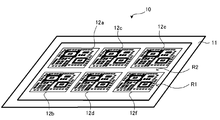
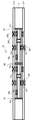
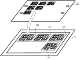
- the wiring board 10 has an insulating substrate 11 as a frame and wiring substrates 12a, 12b, 12c, 12d, and 12e as shown in FIG. 1A and the internal structure in FIG. 1B, for example. , 12f.
- the insulating substrate 11 and the wiring boards 12a to 12f, and the wiring boards 12a to 12f are horizontally arranged via the boundary portions R1 and R2, respectively.
- sixth and fifth insulating layers 313 and 311 are formed on the front and back surfaces of the insulating substrate 11 and the wiring substrates 12a to 12f, respectively.
- FIG. 1B is a diagram illustrating the internal structure of the wiring board 10 with the fifth and sixth insulating layers 311 and 313 omitted.
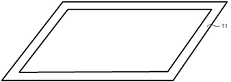
- the insulating substrate 11 is an insulating substrate made of, for example, glass epoxy resin. Specifically, as shown in FIGS. 1A and 1B, the insulating substrate 11 is a rectangular frame surrounding the wiring substrates 12a to 12f. The wiring boards 12a to 12f are disposed inside the insulating board 11.
- the shape of the insulating substrate 11 is arbitrary. For example, it may be a circular shape, an elliptical shape, or two elongated rods that sandwich a wiring board arranged in a row.
- the wiring boards 12a to 12f are rectangular rigid boards. However, the shape of the wiring boards 12a to 12f is arbitrary, and may be, for example, a parallelogram, a circle, or an ellipse. Note that the wiring boards 12a to 12f are not electrically connected to each other.
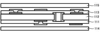
- the wiring boards 12a to 12f are so-called build-up multilayer printed wiring boards as shown in the sectional structure in FIG. That is, the wiring boards 12a to 12f are configured by laminating the rigid base 112, the first and second insulating layers 111 and 113, and the third and fourth insulating layers 114 and 115.
- the rigid base 112 is made of, for example, a rigid insulating material. Specifically, the rigid base 112 is made of, for example, a glass epoxy resin having a thickness of about “50 to 150 ⁇ m”, preferably about “100 ⁇ m”.
- first to fourth insulating layers 111, 113 to 115 made of cured prepreg for example, wiring layers 122a, 122b, 121, 123 to 125 made of copper, and via holes (interlayers) Connection portions) 131, 133 to 135 are formed.
- the via holes 131 and 133 to 135 are filled with conductors 141 and 143 to 145 made of, for example, copper, and electrically connect the wiring layers.
- a through hole 132 is formed in the rigid base material 112. In the through hole 132, a conductor 142 such as copper is plated with a through hole, and the wiring layers 122a and 122b on the front and back of the rigid base 112 are electrically connected.
- wiring layers 122b and 122a are respectively formed on the front and back surfaces of the rigid base 112, and these wiring layers 122a and 122b are respectively connected to the upper layers through the via holes 131 and 133 and the conductors 141 and 143, respectively.
- the wiring layers 121 and 123 are electrically connected.
- the wiring layers 121 and 123 are electrically connected to the upper wiring layers 124 and 125 via the via holes 134 and 135 and the conductors 144 and 145, respectively.
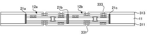
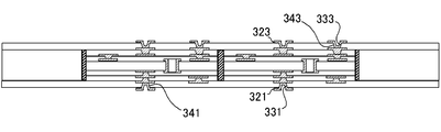
- sixth and fifth insulating layers 313 and 311 are formed, respectively, as shown in FIG. 3 (AA sectional view of FIG. 1A), for example.
- the fifth and sixth insulating layers 311 and 313 cover the boundary portion R1 between the insulating substrate 11 and the wiring substrates 12a to 12f and the boundary portion R2 between the wiring substrates 12a to 12f (see FIGS. 1A and 1B). Be placed. Further, the fifth and sixth insulating layers 311 and 313 are continuously extended from the insulating substrate 11 to the wiring substrates 12a to 12f.
- Via holes 331 and 333 are formed in the fifth and sixth insulating layers 311 and 313, respectively.
- conductors 341 and 343 made of, for example, copper are formed.
- the conductors 341 and 343 are electrically connected to the wiring layers 124 and 125 of the wiring boards 12a to 12f, respectively. Note that the wiring boards 12a to 12f are not electrically connected to each other.
- the fifth and sixth insulating layers 311 and 313 are made of, for example, a rigid insulating material such as a cured prepreg.
- the prepregs of the first to sixth insulating layers 111, 113 to 115, 311, and 313 preferably include a resin having low flow characteristics.
- Such a prepreg can be produced by advancement of the degree of curing in advance by impregnating an epoxy resin into a glass cloth and then thermally curing the resin. Further, the glass cloth may be impregnated with a resin having a high viscosity, the glass cloth may be impregnated with a resin containing an inorganic filler (for example, silica filler), or the resin impregnation amount of the glass cloth may be reduced. Further, RCF (Resin Coated cupper Foil) or the like may be used instead of the prepreg.
- the manufacturing panel 100 is a dedicated manufacturing panel for manufacturing only wiring boards having the same structure (structure shown in FIG. 2), including the wiring boards 12a to 12f.
- the manufacturing method of the present embodiment manufactures the wiring boards 12a to 12f separately from the insulating board 11. Therefore, more wiring boards 12a to 12f can be manufactured on the manufacturing panel 100, and the yield and the number of products can be improved.
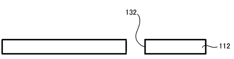
- an operator first cuts a material common to a plurality of products with, for example, a laser or the like to obtain a rigid base 112 having a predetermined shape and size. Prepare.
- a through hole 132 is formed as shown in FIG. 5B by irradiating a CO 2 laser, for example, from a CO 2 laser processing apparatus.
- PN plating for example, chemical copper plating and electrolytic copper plating
- a conductor film is formed on the entire surface of the rigid base 112 including the inside of the through hole 132.
- the conductor film is thinned to a predetermined thickness by, for example, half-etching, and then subjected to, for example, a predetermined lithography process (pretreatment, lamination, exposure, development, etching, stripping, inner layer inspection, etc.)
- the conductor film is patterned as shown in FIG. 5C. Thereby, the wiring layers 122a and 122b and the conductor 142 are formed.
- second and first insulating layers 113 and 111 are arranged on the front and back of the wiring board, respectively. And they are pressure-pressed (for example, hot press). Thereafter, the resin is cured by, for example, heat treatment, and the first and second insulating layers 111 and 113 are solidified. Subsequently, after a predetermined pretreatment, as shown in FIG. 6B, via holes 131 are formed in the first insulating layer 111 and via holes 133 are formed in the second insulating layer 113 by, for example, a laser.
- PN plating for example, chemical copper plating and electrolytic copper plating
- a conductor film is formed on the entire surface of the wiring board including the via holes 131 and 133.
- the conductor film on the surface of the wiring board is thinned to a predetermined thickness by, for example, half-etching, and then subjected to, for example, a predetermined lithography process (pretreatment, lamination, exposure, development, etching, peeling film, inner layer inspection, etc.)
- a predetermined lithography process pretreatment, lamination, exposure, development, etching, peeling film, inner layer inspection, etc.
- the wiring layers 121 and 123 can also be formed by printing a conductive paste (for example, a thermosetting resin containing conductive particles) by, for example, a screen printing method.
- a conductive paste for example, a thermosetting resin containing conductive particles
- fourth and third insulating layers 115 and 114 are arranged on the front and back of the wiring board, respectively. And they are pressure-pressed (for example, hot press). Thereafter, the resin is cured by, for example, heat treatment, and the third and fourth insulating layers 114 and 115 are solidified. Subsequently, after a predetermined pretreatment, as shown in FIG. 7B, via holes 134 are formed in the third insulating layer 114 and via holes 135 are formed in the fourth insulating layer 115 by, for example, a laser. Further, the conductors 144 and 145 and the wiring layers 124 and 125 as shown in FIG. 2 are formed through the same process as the process of FIG. 6C. Thus, as shown in FIG. 4, the wiring boards 12a to 12f are manufactured on the manufacturing panel 100.
- the worker manufactures the insulating board 11. Specifically, as shown in FIG. 8, a material (manufacturing panel 200) common to a plurality of products is cut by, for example, a laser to manufacture an insulating substrate 11 having a predetermined shape and size. As a result, a rectangular frame as shown in FIG. 9 is obtained as the insulating substrate 11. As described above, by manufacturing the insulating substrate 11 separately from the wiring substrates 12a to 12f, an unnecessary stacked body is not formed on the insulating substrate 11. Therefore, consumption of a conductor material, an insulating material, etc. can be reduced. As a result, the manufacturing cost can be reduced.
- the wiring boards 12a to 12f are cut out from the manufacturing panel 100 and placed inside the insulating board 11 as shown in FIG.
- an energization inspection or the like is performed on the wiring boards 12a to 12f.
- the defective substrate is removed and only the good substrate is used. That is, only the good substrate is disposed inside the insulating substrate 11.
- the manufacturing method of this embodiment can find a defective substrate and remove the defective substrate before forming the outermost layer, that is, earlier. Therefore, the consumption of material when a defective substrate occurs can be reduced. As a result, the manufacturing cost can be reduced.
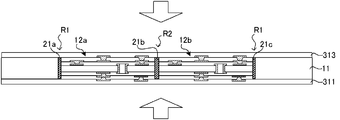
- sixth and fifth insulating layers 313 and 311 are formed on the front and back of the wiring boards 12a to 12f (only 12a and 12b are shown in FIGS. 11A to 11D) and the insulating board 11, respectively. Place. And as shown to FIG. 11B, they are press-pressed (for example, hot press). Thus, the resins 21a to 21c are extruded from the fifth and sixth insulating layers 311 and 313, respectively.
- the resins 21a to 21c (insulating material) ooze out (flow out) from the prepregs constituting the fifth and sixth insulating layers 311 and 313, and the insulating substrate 11 and the wiring substrate 12a to Resins 21a to 21c are filled in the boundary R1 with 12f and the boundary R2 between the wiring boards 12a to 12f, respectively.
- the resins 21a to 21c are filled from both surfaces. Thereafter, the resin is cured, for example, by heat treatment, and the fifth and sixth insulating layers 311 and 313 are solidified.
- via holes 331 are formed in the fifth insulating layer 311 and via holes 333 are formed in the sixth insulating layer 313, for example, by a laser.
- PN plating for example, chemical copper plating and electrolytic copper plating
- a conductor film is formed on the entire surface of the wiring board including the via holes 331 and 333.
- the conductor film on the surface of the wiring board is thinned to a predetermined thickness by, for example, half-etching, and then subjected to, for example, a predetermined lithography process (pretreatment, lamination, exposure, development, etching, peeling film, inner layer inspection, etc.)
- a predetermined lithography process pretreatment, lamination, exposure, development, etching, peeling film, inner layer inspection, etc.
- the outer shape of the wiring board is processed by a router, for example.
- the wiring board is processed into a predetermined shape (for example, a square shape) within the range of the width of the frame of the insulating substrate 11 as indicated by a cut line L1 in the drawing.
- the wiring board 10 as shown in FIG. 3 is manufactured. That is, in the wiring board 10, the fifth and sixth insulating layers 311 and 313 and the wiring layers 321 and 323 are the outermost layers.
- the wiring boards 12a to 12f are not electrically connected to each other, but the present invention is not limited to this.
- the wiring boards 12a to 12f may be electrically connected depending on the application.
- the wiring boards 12a to 12f are not limited to those shown in FIG.
- a flexible wiring board may be used.
- a flex-rigid wiring board 101 having a flexible portion 101a and rigid portions 101b and 101c as shown in FIG. 13A may be used.
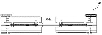
- a wiring board 102 incorporating an electronic component 102a as shown in FIG. 13B may be used.
- a wiring board 103 having a cavity 103a formed on the surface thereof may be used.
- FIG. 14 cross-sectional view corresponding to FIG. 3
- single-sided wiring boards 104a and 104b in which a wiring layer or an insulating layer is laminated only on one side of the core may be used.
- the material, size, number of layers, etc. of each layer can be arbitrarily changed.
- the single insulating layers that is, the sixth and fifth insulating layers 313 and 311 are formed on the front and back surfaces of the insulating substrate 11 and the wiring substrates 12a to 12f, respectively, but the present invention is not limited to this.
- a plurality of insulating layers made of different materials that is, sixth and eighth insulating layers 313 and 315, fifth and seventh, respectively.
- the insulating layers 311 and 314 may be formed.
- the wiring board 10 including the six wiring boards 12a to 12f is illustrated, but the number of wiring boards is arbitrary. That is, for example, it may be one, two to five, or seven or more.
- the wiring board of the present invention is suitable for forming an electric circuit. Moreover, the manufacturing method of the wiring board of this invention is suitable for manufacture of a wiring board.
- Wiring board 11 Insulating substrate 12a to 12f Wiring substrate 21a to 21c Resin (insulating material) 100, 200 Manufacturing panel 111 First insulating layer 112 Rigid base material 113 Second insulating layer 114 Third insulating layer 115 Fourth insulating layer 121, 123, 124, 125 Wiring layer (conductor pattern) 122a, 122b Wiring layer (conductor pattern) 131, 133, 134, 135 Via hole (interlayer connection) 132 through-hole 141-145 conductor 311 5th insulating layer (insulating layer) 313 Sixth insulating layer (insulating layer) 314 Seventh insulating layer (insulating layer) 315 Eighth insulating layer (insulating layer) 321, 323 Wiring layer (conductor pattern) 331, 333 Via hole 341, 343 Conductor R1, R2 boundary
Landscapes
- Engineering & Computer Science (AREA)
- Microelectronics & Electronic Packaging (AREA)
- Manufacturing & Machinery (AREA)
- Production Of Multi-Layered Print Wiring Board (AREA)
- Structure Of Printed Boards (AREA)
Abstract
Description
11 絶縁基板
12a~12f 配線基板
21a~21c 樹脂(絶縁材料)
100、200 製造パネル
111 第1の絶縁層
112 リジッド基材
113 第2の絶縁層
114 第3の絶縁層
115 第4の絶縁層
121、123、124、125 配線層(導体パターン)
122a、122b 配線層(導体パターン)
131、133、134、135 バイアホール(層間接続部)
132 スルーホール
141~145 導体
311 第5の絶縁層(絶縁層)
313 第6の絶縁層(絶縁層)
314 第7の絶縁層(絶縁層)
315 第8の絶縁層(絶縁層)
321、323 配線層(導体パターン)
331、333 バイアホール
341、343 導体
R1、R2 境界部
Claims (12)
- 導体パターンを有する配線基板と、
前記配線基板と並んで配置された絶縁基板と、
前記導体パターンに電気的に接続されためっきによる導体が形成されたバイアホールを有し、前記絶縁基板と前記配線基板の境界部を被覆するように、前記絶縁基板から前記配線基板に連続して延設された絶縁層と、
からなる配線板において、
前記絶縁基板と前記配線基板との境界部には、前記絶縁層を構成する絶縁材料が充填されている、
ことを特徴とする配線板。 - 前記絶縁層は、樹脂を含み、
前記絶縁材料は、前記絶縁層から流出した前記樹脂である、
ことを特徴とする請求項1に記載の配線板。 - 前記絶縁層は、前記絶縁基板及び前記配線基板の両面に形成される、
ことを特徴とする請求項1に記載の配線板。 - 前記配線基板を、複数備える、
ことを特徴とする請求項1に記載の配線板。 - 前記配線基板同士は、互いに電気的に接続されない、
ことを特徴とする請求項4に記載の配線板。 - 前記絶縁層は、複数の絶縁材料からなる、
ことを特徴とする請求項1に記載の配線板。 - 前記絶縁層は、前記配線板の絶縁層の一部を構成する、
ことを特徴とする請求項1に記載の配線板。 - 絶縁材料からなる絶縁基板と、配線層を有する配線基板とを、水平に配置することと、
前記絶縁基板及び前記配線基板の境界部を被覆して絶縁層を配置することと、
前記絶縁基板と前記配線基板との境界部に、前記絶縁層を構成する前記絶縁材料を充填することと、
前記絶縁層にバイアホールを形成し、さらに該バイアホールにめっきにより導体を形成することと、
前記バイアホールに形成された前記導体と前記配線層とを、電気的に接続することと、
を含む、
ことを特徴とする配線板の製造方法。 - 外形加工を行うことをさらに含む、
ことを特徴とする請求項8に記載の配線板の製造方法。 - 前記絶縁層は、前記絶縁材料としての樹脂を含み、
前記絶縁層をプレスすることにより、前記絶縁層から前記樹脂を押し出して、前記絶縁基板と前記配線基板との間に充填する、
ことを特徴とする請求項8に記載の配線板の製造方法。 - 前記絶縁基板及び前記配線基板を、それぞれ異なる製造パネルを用いて製造することをさらに含む、
ことを特徴とする請求項8に記載の配線板の製造方法。 - 前記外形加工はルーター加工である、
ことを特徴とする請求項9に記載の配線板の製造方法。
Priority Applications (2)
| Application Number | Priority Date | Filing Date | Title |
|---|---|---|---|
| CN2009801476864A CN102227959B (zh) | 2008-11-28 | 2009-11-17 | 配线板及其制造方法 |
| JP2010540452A JPWO2010061752A1 (ja) | 2008-11-28 | 2009-11-17 | 配線板及びその製造方法 |
Applications Claiming Priority (2)
| Application Number | Priority Date | Filing Date | Title |
|---|---|---|---|
| JP2008-304665 | 2008-11-28 | ||
| JP2008304665 | 2008-11-28 |
Publications (1)
| Publication Number | Publication Date |
|---|---|
| WO2010061752A1 true WO2010061752A1 (ja) | 2010-06-03 |
Family
ID=42221760
Family Applications (1)
| Application Number | Title | Priority Date | Filing Date |
|---|---|---|---|
| PCT/JP2009/069480 Ceased WO2010061752A1 (ja) | 2008-11-28 | 2009-11-17 | 配線板及びその製造方法 |
Country Status (6)
| Country | Link |
|---|---|
| US (2) | US8921705B2 (ja) |
| JP (1) | JPWO2010061752A1 (ja) |
| KR (1) | KR20110081856A (ja) |
| CN (1) | CN102227959B (ja) |
| TW (1) | TW201038153A (ja) |
| WO (1) | WO2010061752A1 (ja) |
Families Citing this family (6)
| Publication number | Priority date | Publication date | Assignee | Title |
|---|---|---|---|---|
| KR101051491B1 (ko) | 2009-10-28 | 2011-07-22 | 삼성전기주식회사 | 다층 경연성 인쇄회로기판 및 다층 경연성 인쇄회로기판의 제조방법 |
| US20130025914A1 (en) * | 2011-07-25 | 2013-01-31 | Ibiden Co., Ltd. | Wiring board and method for manufacturing the same |
| TWI461127B (zh) * | 2012-12-25 | 2014-11-11 | Univ Nat Taipei Technology | 電子裝置及其製法 |
| EP3282467B1 (en) * | 2015-04-07 | 2019-10-23 | SOC Corporation | Fuse production method, fuse, circuit board production method and circuit board |
| JP6815880B2 (ja) * | 2017-01-25 | 2021-01-20 | 株式会社ディスコ | 半導体パッケージの製造方法 |
| CN112449484B (zh) * | 2019-08-30 | 2022-05-27 | 庆鼎精密电子(淮安)有限公司 | 电路板及其制造方法 |
Citations (4)
| Publication number | Priority date | Publication date | Assignee | Title |
|---|---|---|---|---|
| JPH0897564A (ja) * | 1994-09-27 | 1996-04-12 | Matsushita Electric Works Ltd | 多層配線板及びその製造方法 |
| JP2003069190A (ja) * | 2001-08-30 | 2003-03-07 | Ibiden Co Ltd | 多ピース基板 |
| JP2004087786A (ja) * | 2002-08-27 | 2004-03-18 | Dt Circuit Technology Co Ltd | プリント配線板の製造方法、プリント配線板の製造装置、プリント配線板 |
| JP2007067369A (ja) * | 2005-08-05 | 2007-03-15 | Ngk Spark Plug Co Ltd | 配線基板及びその製造方法、埋め込み用セラミックチップ |
Family Cites Families (15)
| Publication number | Priority date | Publication date | Assignee | Title |
|---|---|---|---|---|
| US6835895B1 (en) * | 1996-12-19 | 2004-12-28 | Ibiden Co., Ltd. | Printed wiring board and method for manufacturing the same |
| JP4945842B2 (ja) | 2000-04-05 | 2012-06-06 | イビデン株式会社 | プリント配線板及びプリント配線板の製造方法 |
| JP2002232089A (ja) | 2001-01-30 | 2002-08-16 | Ibiden Denshi Kogyo Kk | 多ピース基板およびその製造方法 |
| JP4249910B2 (ja) | 2001-03-26 | 2009-04-08 | イビデン株式会社 | 多ピース基板およびその製造方法 |
| JP2002344146A (ja) | 2001-05-15 | 2002-11-29 | Tdk Corp | 高周波モジュールとその製造方法 |
| US20040231885A1 (en) * | 2003-03-07 | 2004-11-25 | Borland William J. | Printed wiring boards having capacitors and methods of making thereof |
| JP2005322878A (ja) | 2004-04-09 | 2005-11-17 | Dainippon Printing Co Ltd | 印刷配線基板の組付パネル、印刷配線基板の実装用単位シート、リジッド−フレキシブル基板及びこれらの製造方法 |
| CN100367491C (zh) * | 2004-05-28 | 2008-02-06 | 日本特殊陶业株式会社 | 中间基板 |
| US7919844B2 (en) * | 2005-05-26 | 2011-04-05 | Aprolase Development Co., Llc | Tier structure with tier frame having a feedthrough structure |
| US7932471B2 (en) * | 2005-08-05 | 2011-04-26 | Ngk Spark Plug Co., Ltd. | Capacitor for incorporation in wiring board, wiring board, method of manufacturing wiring board, and ceramic chip for embedment |
| JP4923510B2 (ja) | 2005-10-19 | 2012-04-25 | 大日本印刷株式会社 | リジッド−フレキシブル基板及びその製造方法 |
| JP4648230B2 (ja) | 2006-03-24 | 2011-03-09 | 日本特殊陶業株式会社 | 配線基板の製造方法 |
| JP4518114B2 (ja) * | 2007-07-25 | 2010-08-04 | Tdk株式会社 | 電子部品内蔵基板及びその製造方法 |
| JP4518113B2 (ja) * | 2007-07-25 | 2010-08-04 | Tdk株式会社 | 電子部品内蔵基板及びその製造方法 |
| JP2009147263A (ja) * | 2007-12-18 | 2009-07-02 | Shinko Electric Ind Co Ltd | 配線基板およびその製造方法 |
-
2009
- 2009-08-07 US US12/537,607 patent/US8921705B2/en active Active
- 2009-11-17 KR KR1020117011338A patent/KR20110081856A/ko not_active Ceased
- 2009-11-17 CN CN2009801476864A patent/CN102227959B/zh not_active Expired - Fee Related
- 2009-11-17 WO PCT/JP2009/069480 patent/WO2010061752A1/ja not_active Ceased
- 2009-11-17 JP JP2010540452A patent/JPWO2010061752A1/ja active Pending
- 2009-11-27 TW TW098140694A patent/TW201038153A/zh unknown
-
2014
- 2014-07-10 US US14/327,836 patent/US20140318848A1/en not_active Abandoned
Patent Citations (4)
| Publication number | Priority date | Publication date | Assignee | Title |
|---|---|---|---|---|
| JPH0897564A (ja) * | 1994-09-27 | 1996-04-12 | Matsushita Electric Works Ltd | 多層配線板及びその製造方法 |
| JP2003069190A (ja) * | 2001-08-30 | 2003-03-07 | Ibiden Co Ltd | 多ピース基板 |
| JP2004087786A (ja) * | 2002-08-27 | 2004-03-18 | Dt Circuit Technology Co Ltd | プリント配線板の製造方法、プリント配線板の製造装置、プリント配線板 |
| JP2007067369A (ja) * | 2005-08-05 | 2007-03-15 | Ngk Spark Plug Co Ltd | 配線基板及びその製造方法、埋め込み用セラミックチップ |
Also Published As
| Publication number | Publication date |
|---|---|
| JPWO2010061752A1 (ja) | 2012-04-26 |
| CN102227959A (zh) | 2011-10-26 |
| US8921705B2 (en) | 2014-12-30 |
| TW201038153A (en) | 2010-10-16 |
| KR20110081856A (ko) | 2011-07-14 |
| US20100132980A1 (en) | 2010-06-03 |
| CN102227959B (zh) | 2013-07-31 |
| US20140318848A1 (en) | 2014-10-30 |
Similar Documents
| Publication | Publication Date | Title |
|---|---|---|
| TWI507099B (zh) | 剛撓結合板及其製作方法、電路板模組 | |
| JP5059950B2 (ja) | 配線板及びその製造方法 | |
| US8863379B2 (en) | Methods of manufacturing printed circuit boards using parallel processes to interconnect with subassemblies | |
| TWI466610B (zh) | 封裝結構及其製作方法 | |
| CN103379750B (zh) | 多层电路板及其制作方法 | |
| CN101472404A (zh) | 多层电路板及其制作方法 | |
| TW201406224A (zh) | 多層線路板及其製作方法 | |
| JPWO2010061752A1 (ja) | 配線板及びその製造方法 | |
| US20140182899A1 (en) | Rigid-flexible printed circuit board and method for manufacturing same | |
| KR20130098921A (ko) | 다층 배선기판 및 그 제조방법 | |
| TW201406222A (zh) | 多層線路板及其製作方法 | |
| JP2014068047A (ja) | 多層プリント配線板の製造方法 | |
| KR101097504B1 (ko) | 다층 인쇄 회로 기판의 제조방법 | |
| JP5057653B2 (ja) | フレックスリジッド配線基板及びその製造方法 | |
| JP2010205809A (ja) | 多層プリント配線板およびその製造方法 | |
| TWI461135B (zh) | 製作電路板之方法 | |
| KR100651422B1 (ko) | 일괄 적층 방식을 이용한 다층 인쇄회로기판의 제조 방법 | |
| JP2000216544A (ja) | メタルコアbvh用多層シ―ルド板の製造方法 | |
| CN112261792B (zh) | 一种改善钻孔毛刺的pcb制作方法及pcb | |
| TW201125455A (en) | Method for manufacturing printed circuit board | |
| US20150366081A1 (en) | Manufacturing method for circuit structure embedded with electronic device | |
| JP2019067821A (ja) | プリント配線板の製造方法 | |
| JP2012248782A (ja) | 多層フレキシブルプリント配線板の製造方法 | |
| JP2005026548A (ja) | マルチワイヤ配線板の製造方法 | |
| KR20130008290A (ko) | 기판 제조용 캐리어 및 이를 이용한 인쇄회로기판의 제조방법 |
Legal Events
| Date | Code | Title | Description |
|---|---|---|---|
| WWE | Wipo information: entry into national phase |
Ref document number: 200980147686.4 Country of ref document: CN |
|
| 121 | Ep: the epo has been informed by wipo that ep was designated in this application |
Ref document number: 09829000 Country of ref document: EP Kind code of ref document: A1 |
|
| ENP | Entry into the national phase |
Ref document number: 2010540452 Country of ref document: JP Kind code of ref document: A |
|
| ENP | Entry into the national phase |
Ref document number: 20117011338 Country of ref document: KR Kind code of ref document: A |
|
| NENP | Non-entry into the national phase |
Ref country code: DE |
|
| 122 | Ep: pct application non-entry in european phase |
Ref document number: 09829000 Country of ref document: EP Kind code of ref document: A1 |