WO2010055841A1 - サーミスタ及びその製造方法 - Google Patents
サーミスタ及びその製造方法 Download PDFInfo
- Publication number
- WO2010055841A1 WO2010055841A1 PCT/JP2009/069167 JP2009069167W WO2010055841A1 WO 2010055841 A1 WO2010055841 A1 WO 2010055841A1 JP 2009069167 W JP2009069167 W JP 2009069167W WO 2010055841 A1 WO2010055841 A1 WO 2010055841A1
- Authority
- WO
- WIPO (PCT)
- Prior art keywords
- thermistor
- comb
- resistance value
- thin film
- additional electrode
- Prior art date
- Legal status (The legal status is an assumption and is not a legal conclusion. Google has not performed a legal analysis and makes no representation as to the accuracy of the status listed.)
- Ceased
Links
Images


Classifications
-
- H—ELECTRICITY
- H01—ELECTRIC ELEMENTS
- H01C—RESISTORS
- H01C7/00—Non-adjustable resistors formed as one or more layers or coatings; Non-adjustable resistors made from powdered conducting material or powdered semi-conducting material with or without insulating material
- H01C7/008—Thermistors
-
- G—PHYSICS
- G01—MEASURING; TESTING
- G01K—MEASURING TEMPERATURE; MEASURING QUANTITY OF HEAT; THERMALLY-SENSITIVE ELEMENTS NOT OTHERWISE PROVIDED FOR
- G01K7/00—Measuring temperature based on the use of electric or magnetic elements directly sensitive to heat ; Power supply therefor, e.g. using thermoelectric elements
- G01K7/16—Measuring temperature based on the use of electric or magnetic elements directly sensitive to heat ; Power supply therefor, e.g. using thermoelectric elements using resistive elements
- G01K7/22—Measuring temperature based on the use of electric or magnetic elements directly sensitive to heat ; Power supply therefor, e.g. using thermoelectric elements using resistive elements the element being a non-linear resistance, e.g. thermistor
- G01K7/226—Measuring temperature based on the use of electric or magnetic elements directly sensitive to heat ; Power supply therefor, e.g. using thermoelectric elements using resistive elements the element being a non-linear resistance, e.g. thermistor using microstructures, e.g. silicon spreading resistance
-
- H—ELECTRICITY
- H01—ELECTRIC ELEMENTS
- H01C—RESISTORS
- H01C1/00—Details
- H01C1/14—Terminals or tapping points specially adapted for resistors; Arrangements of terminals or tapping points on resistors
-
- H—ELECTRICITY
- H01—ELECTRIC ELEMENTS
- H01C—RESISTORS
- H01C1/00—Details
- H01C1/14—Terminals or tapping points specially adapted for resistors; Arrangements of terminals or tapping points on resistors
- H01C1/142—Terminals or tapping points specially adapted for resistors; Arrangements of terminals or tapping points on resistors the terminals or tapping points being coated on the resistive element
Definitions
- the present invention relates to a thermistor used for temperature detection sensors of various electronic devices and a method of manufacturing the same.
- Thermisters are temperature sensors composed of oxide semiconductors whose resistance value changes with temperature, and are widely used in temperature compensation circuits and the like.
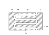
- This thermistor has, for example, a structure in which a pair of comb-like electrodes are formed to be opposed to each other on an oxide semiconductor. Specifically, as shown in FIG. 4, the comb portions 12 a and 13 a are opposed to each other at a predetermined distance on the oxide semiconductor base material 11 (the other comb portion between the comb portions 12 a of one comb electrode 12 is Is disposed so as to be inserted) (Patent Document 1: FIG. 2).
- the resistance value of the thermistor is determined by the specific resistance of the oxide semiconductor and the contact area between the comb electrodes 12 and 13 and the oxide semiconductor substrate 11.
- the thermistor Since the thermistor is usually used in a temperature compensation circuit or the like, it is required that its resistance value be more accurate. For this reason, after forming the comb-tooth electrode on the oxide semiconductor base material, in order to obtain a desired resistance value, resistance value adjustment is performed as necessary. For example, as described in Patent Document 1, as the resistance value adjustment, the comb portion 12a of the comb electrode 12 is partially removed (removed portion 14) to increase the resistance value.
- the present invention has been made in view of the foregoing, and it is an object of the present invention to provide a thermistor precisely adjusted to a desired resistance value without damaging the thermistor substrate, and a method of manufacturing the same.
- the thermistor according to the present invention comprises a substrate, a thermistor thin film formed on the substrate, and a pair of comb-like electrodes formed on the thermistor thin film and provided to face each other,
- the comb-tooth electrode is characterized by having an additional electrode portion added to have a desired resistance value.
- the additional electrode portion is provided to extend along the longitudinal direction of the comb portion of the comb electrode.
- the method for manufacturing a thermistor according to the present invention comprises the steps of: forming a thermistor thin film on a substrate; and forming a pair of comb-like electrodes on the thermistor thin film having a pattern such that the thermistor has a resistance value higher than a target resistance value. And forming an additional electrode portion on the comb-tooth electrode so that the thermistor has the target resistance value.
- the resistance value of the thermistor is lowered and adjusted by providing the additional electrode portion to the comb electrode, so that the thermistor thin film is damaged as in the case of removing the comb electrode by laser trimming or sandblasting. There is no. Therefore, it is possible to realize a thermistor adjusted to a desired resistance value with high accuracy without damaging the thermistor thin film.
- the additional electrode portion is formed in a size determined from the relationship between the dimension of the additional electrode portion and the resistance value.
- a thermistor thin film is formed on a substrate, and a pair of comb-like electrodes having a pattern such that the thermistor has a resistance value higher than a target resistance value are opposed to each other on the thermistor thin film. Since it is obtained by forming an additional electrode portion on the comb electrode so that the thermistor has the target resistance value, it can be adjusted to a desired resistance value with high accuracy without damaging the thermistor substrate. Can be realized.
- FIG. 1 It is a figure which shows the thermistor concerning embodiment of this invention, (a) is a top view, (b) is an enlarged view of the additional electrode part in (a). It is a figure which shows the relationship between length L of an additional electrode part and resistance value in the thermistor which concerns on embodiment of this invention.
- (A) to (f) are diagrams for explaining a method of manufacturing a thermistor according to an embodiment of the present invention. It is a figure for demonstrating the conventional thermistor.
- FIG. 1 is a view showing a thermistor according to an embodiment of the present invention, where (a) is a plan view and (b) is an enlarged view of an additional electrode portion in (a).
- the thermistor shown in FIG. 1 mainly includes an insulating substrate 1, a thermistor thin film 2 formed on the insulating substrate 1, and a pair of comb electrodes 3 and 4 formed on the thermistor thin film 2.
- As the substrate instead of the insulating substrate 1, a substrate formed by forming an insulating film on a conductive substrate may be used.
- the pair of comb electrodes 3 and 4 are arranged to face each other.
- the pair of comb electrodes 3 and 4 are arranged such that the comb 4 a of the other comb electrode 4 is inserted between the combs 3 a of the one comb electrode 3. Therefore, the comb portion 3a of one of the comb electrodes 3 and the comb portion 4a of the other comb electrode 4 are formed to be substantially the same in the longitudinal direction and to be spaced apart from each other by a predetermined distance. Further, the contact area (overlap area) between the comb-tooth electrodes 3 and 4 and the thermistor thin film 2 is appropriately determined in order to achieve a desired resistance value (target resistance value) in consideration of the specific resistance of the thermistor thin film 2. It can be changed.
- the contact area (overlap area) between the comb-tooth electrodes 3 and 4 and the thermistor thin film 2 and the pattern of the comb-tooth electrodes 3 and 4 have a desired resistance value (target resistance value). And can be changed as appropriate.
- the comb-tooth electrodes 3 and 4 (here, the comb-tooth electrode 4) have additional electrode portions 5 so as to have a desired resistance value.
- the additional electrode portion 5 By providing the additional electrode portion 5, the contact area between the thermistor thin film 2 and the comb electrode 4 becomes large, and as a result, the resistance value can be lowered.
- the present inventors examined the resistance value of the thermistor when the length L of the additional electrode portion 5 was changed using a thermistor as shown in FIG.
- the width D1 of the thermistor thin film 2 is 140 ⁇ m
- the length W1 of the thermistor thin film 2 is 240 ⁇ m
- the width W2 of the contact area between the thermistor thin film 2 and the comb electrode is 130 ⁇ m
- the length D2 of the contact area between the electrodes is 10 ⁇ m
- the pad width W4 of the comb electrodes is 70 ⁇ m
- the inter-pad distance W3 of the comb electrodes is 220 ⁇ m
- the distance between the comb electrodes (comb 3a and comb 4a The distance between them is 10.9 ⁇ m
- the width of the comb-tooth electrode (the width of the comb portions 3a and 4a) is 10 ⁇ m.
- the specific resistance of the thermistor thin film 2 was 0.25 k ⁇ ⁇ cm, and the thickness of the thermistor thin film 2 was 0.75 ⁇ m. The results are shown in FIG. As can be seen from FIG. 2, the resistance value decreases as the length L of the additional electrode portion 5 is increased.
- the present inventors previously formed a pair of comb-like electrodes having a pattern having a resistance value higher than the target resistance value on the thermistor thin film, and thereafter providing an additional electrode portion, By lowering the resistance value and adjusting to the target resistance value, it has been found that the thermistor whose resistance value is accurately adjusted can be obtained without damaging the thermistor thin film.
- a thermistor thin film is formed on a substrate, and a pair of comb-like electrodes having patterns such that the thermistor has a resistance value higher than a target resistance value are opposed to each other on the thermistor thin film.
- the comb-tooth electrode is provided to have a resistance value higher than the target resistance value, and the desired resistance value is obtained using the relationship shown in FIG. 2 (the relationship between the dimension of the additional electrode portion and the resistance value).
- the size of the additional electrode portion (in this case, the length L of the additional electrode portion) is determined, and the additional electrode portion of that length is provided on the comb electrode.
- the additional electrode portion is provided to adjust the resistance value, the thermistor thin film itself is not damaged. This makes it possible to obtain a thermistor precisely adjusted to a desired resistance value without damaging the thermistor substrate.
- the additional electrode portion 5 is preferably formed to have a width wider than the width of the comb portion 4 a of the comb electrode 4 as shown in FIG. 1 (b). Thereby, the alignment shift at the time of formation of the additional electrode part 5 can be accept
- the additional electrode portion 5 has a width which is about several microns wider than the width of the comb portion 4 a of the comb electrode 4.
- the additional electrode portion 5 is wider by 2 ⁇ m to 3 ⁇ m on both sides than the comb portion 4a.
- a material constituting the thermistor thin film 2 in the case of an NTC (Negative Temperature Coefficient) thermistor, a ceramic semiconductor containing an oxide of a metal such as manganese, nickel or cobalt can be used, and a PTC (Positive Temperature Coefficient) thermistor
- a ceramic semiconductor or the like containing barium titanate can be used
- a CTR (Critical Temperature Resistor) thermistor a ceramic semiconductor or the like containing vanadium oxide can be used.
- electrode materials such as Cu, Al, Au, Pt, Pd, can be used.
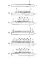
- 3 (a) to 3 (f) are diagrams for explaining the method of manufacturing the thermistor according to the embodiment of the present invention.
- 3 (a) to 3 (f) are cross-sectional views taken along the line III-III in FIG. 1 (a).
- the thermistor thin film 2 is formed on the insulating substrate 1.
- the thermistor thin film 2 is formed on the insulating substrate 1, a resist layer is formed thereon, and exposure is performed using a mask having a pattern of the thermistor thin film to develop the resist layer. Thereafter, milling is performed to form the shape shown in FIG.
- a resist layer 6 is formed on the thermistor thin film 2, and the resist layer 6 is exposed using a mask having a pattern of comb-like electrodes, and the resist layer 6 is developed, as shown in FIG.
- the resist layer 6 is left in the region where the comb electrode is not provided.
- a material for a comb electrode is deposited thereon, and then the resist layer 6 is removed and lifted off.
- the comb-tooth electrodes 3 and 4 having the comb parts 3a and 4a are formed on the thermistor thin film 2.
- the patterns of the comb-tooth electrodes 3 and 4 are designed in advance so that the thermistor has a resistance value higher than the target resistance value.
- a resist layer 6 is formed on the comb-tooth electrodes 3 and 4, and the resist layer 6 is exposed using a mask having a pattern of an additional electrode portion, and the resist layer 6 is developed, as shown in FIG. Thus, the resist layer 6 is left in the region where the additional electrode portion 5 is not provided.
- a material for an additional electrode portion is deposited thereon, and then the resist layer 6 is removed and lifted off. Thereby, as shown in FIG. 3F, the additional electrode portion 5 is formed on the comb portion 4a of the comb electrode 4.
- the length of the additional electrode portion 5 is appropriately set so that the thermistor has a desired resistance value (target resistance value) based on the relationship shown in FIG.
- the formation of the additional electrode portion for adjusting the resistance value is performed by lift-off, so that the thermal damage to the thermistor thin film 2 can be minimized. For this reason, it is possible to obtain a thermistor adjusted to a desired resistance value with high accuracy without damaging the thermistor thin film 2.
- the present invention is not limited to the above embodiment, and can be implemented with various modifications.
- the dimensions, the material, the shape, and the layer forming process in the above embodiment can be appropriately changed without departing from the effects of the present invention.
Landscapes
- Engineering & Computer Science (AREA)
- Microelectronics & Electronic Packaging (AREA)
- Physics & Mathematics (AREA)
- Chemical & Material Sciences (AREA)
- Crystallography & Structural Chemistry (AREA)
- Nonlinear Science (AREA)
- General Physics & Mathematics (AREA)
- Electromagnetism (AREA)
- Thermistors And Varistors (AREA)
Abstract
サーミスタ基材を損傷することなく、所望の抵抗値に高精度に調整されたサーミスタ及びその製造方法を提供すること。本発明のサーミスタの製造方法は、絶縁基板(1)上にサーミスタ薄膜(2)を形成する工程と、サーミスタが目標抵抗値よりも高い抵抗値を有するようなパターンを持つ一対の櫛歯電極(3)、(4)を、前記サーミスタ薄膜(2)上に、互いに対向するように形成する工程と、前記サーミスタが前記目標抵抗値を有するように、前記櫛歯電極(3)、(4)に付加電極部(5)を形成する工程と、を具備することを特徴とする。
Description
本発明は、各種電子機器の温度検知センサに用いられるサーミスタ及びその製造方法に関する。
サーミスタは、温度によって抵抗値が変わる酸化物半導体で構成された温度センサであり、温度補償回路などに広く用いられている。このサーミスタは、例えば、酸化物半導体上に、一対の櫛歯電極を互いに対向するように形成してなる構成を有する。具体的には、図4に示すように、酸化物半導体基材11上に、互いに櫛部12a,13aが所定の間隔をおいて対向するように(一方の櫛歯電極12の櫛部12a間に他方の櫛歯電極13の櫛部13aが挿入するように配置されて)形成されている(特許文献1:図2)。サーミスタの抵抗値は、酸化物半導体の固有抵抗と、櫛歯電極12,13と酸化物半導体基材11との間の接触面積で決定される。
サーミスタは、通常、温度補償回路などに用いられるものであるため、その抵抗値については、より高い精度を有することが求められている。このため、酸化物半導体基材上に櫛歯電極を形成した後に、所望の抵抗値とするために、必要に応じて抵抗値調整が行われる。例えば、特許文献1に記載されているように、抵抗値調整として、櫛歯電極12の櫛部12aを部分的に除去(除去部14)して抵抗値を高くしている。
しかしながら、特許文献1に記載された方法においては、櫛歯電極の櫛部を除去する際に、レーザートリミングやサンドブラストなどの方法が採られている。レーザートリミングやサンドブラストで櫛歯電極の櫛部を除去すると、櫛歯電極の下の酸化物半導体基材を損傷してしまい、抵抗値を調整しているにも拘わらず、結果としてサーミスタの特性が変わってしまう恐れがある。
本発明はかかる点に鑑みてなされたものであり、サーミスタ基材を損傷することなく、所望の抵抗値に高精度に調整されたサーミスタ及びその製造方法を提供することを目的とする。
本発明のサーミスタは、基板と、前記基板上に形成されたサーミスタ薄膜と、前記サーミスタ薄膜上に形成されており、互いに対向するように設けられた一対の櫛歯電極と、を具備し、前記櫛歯電極は、所望の抵抗値を有するように付加された付加電極部を有することを特徴とする。
本発明のサーミスタにおいては、前記付加電極部のサイズは、前記付加電極部の寸法と抵抗値との間の関係から求められたサイズであることが好ましい。
本発明のサーミスタにおいては、前記付加電極部は、前記櫛歯電極の櫛部の幅よりも広い幅を有することが好ましい。
本発明のサーミスタにおいては、前記付加電極部は、前記櫛歯電極の櫛部の長手方向に沿って延在するように設けられることが好ましい。
本発明のサーミスタの製造方法は、基板上にサーミスタ薄膜を形成する工程と、サーミスタが目標抵抗値よりも高い抵抗値を有するようなパターンを持つ一対の櫛歯電極を、前記サーミスタ薄膜上に、互いに対向するように形成する工程と、前記サーミスタが前記目標抵抗値を有するように、前記櫛歯電極に付加電極部を形成する工程と、を具備することを特徴とする。
この方法によれば、櫛歯電極に付加電極部を設けることにより、サーミスタの抵抗値を下げて調整するので、レーザートリミングやサンドブラストで櫛歯電極を除去する際のようにサーミスタ薄膜を損傷させることはない。このため、サーミスタ薄膜を損傷することなく、所望の抵抗値に高精度に調整されたサーミスタを実現することができる。
本発明のサーミスタの製造方法においては、前記付加電極部は、前記付加電極部の寸法と抵抗値との間の関係から求められたサイズで形成することが好ましい。
本発明のサーミスタは、基板上にサーミスタ薄膜を形成し、サーミスタが目標抵抗値よりも高い抵抗値を有するようなパターンを持つ一対の櫛歯電極を、前記サーミスタ薄膜上に、互いに対向するように形成し、前記サーミスタが前記目標抵抗値を有するように、前記櫛歯電極に付加電極部を形成することにより得られるので、サーミスタ基材を損傷することなく、所望の抵抗値に高精度に調整されたサーミスタを実現することができる。
以下、本発明の実施の形態について添付図面を参照して詳細に説明する。
図1は、本発明の実施の形態に係るサーミスタを示す図であり、(a)は平面図であり、(b)は(a)における付加電極部の拡大図である。図1に示すサーミスタは、絶縁基板1と、絶縁基板1上に形成されたサーミスタ薄膜2と、サーミスタ薄膜2上に形成された一対の櫛歯電極3,4と、から主に構成されている。なお、基板としては、絶縁基板1の代わりに、導電性基板上に絶縁膜を形成してなる基板を用いても良い。一対の櫛歯電極3,4は、互いに対向するように配置されている。すなわち、一対の櫛歯電極3,4は、一方の櫛歯電極3の櫛部3a間に他方の櫛歯電極4の櫛部4aが挿入するように配置されている。したがって、一方の櫛歯電極3の櫛部3aと、他方の櫛歯電極4の櫛部4aとは、その長手方向を略同じとし、互いに所定の間隔をおいて位置するように形成されている。また、櫛歯電極3,4とサーミスタ薄膜2との間の接触面積(オーバーラップ面積)は、サーミスタ薄膜2の固有抵抗を考慮して所望の抵抗値(目標抵抗値)を達成するために適宜変更することができる。すなわち、櫛歯電極3,4とサーミスタ薄膜2との間の接触面積(オーバーラップ面積)や、櫛歯電極3,4のパターンは、この所望の抵抗値(目標抵抗値)を実現するために、適宜変更することができる。
図1は、本発明の実施の形態に係るサーミスタを示す図であり、(a)は平面図であり、(b)は(a)における付加電極部の拡大図である。図1に示すサーミスタは、絶縁基板1と、絶縁基板1上に形成されたサーミスタ薄膜2と、サーミスタ薄膜2上に形成された一対の櫛歯電極3,4と、から主に構成されている。なお、基板としては、絶縁基板1の代わりに、導電性基板上に絶縁膜を形成してなる基板を用いても良い。一対の櫛歯電極3,4は、互いに対向するように配置されている。すなわち、一対の櫛歯電極3,4は、一方の櫛歯電極3の櫛部3a間に他方の櫛歯電極4の櫛部4aが挿入するように配置されている。したがって、一方の櫛歯電極3の櫛部3aと、他方の櫛歯電極4の櫛部4aとは、その長手方向を略同じとし、互いに所定の間隔をおいて位置するように形成されている。また、櫛歯電極3,4とサーミスタ薄膜2との間の接触面積(オーバーラップ面積)は、サーミスタ薄膜2の固有抵抗を考慮して所望の抵抗値(目標抵抗値)を達成するために適宜変更することができる。すなわち、櫛歯電極3,4とサーミスタ薄膜2との間の接触面積(オーバーラップ面積)や、櫛歯電極3,4のパターンは、この所望の抵抗値(目標抵抗値)を実現するために、適宜変更することができる。
櫛歯電極3,4(ここでは櫛歯電極4)は、所望の抵抗値を有するように付加電極部5を有する。この付加電極部5を設けることにより、サーミスタ薄膜2と櫛歯電極4との間の接触面積が大きくなり、結果として抵抗値を下げることができる。
本発明者らは、図1に示すようなサーミスタを用い、付加電極部5の長さLを変えたときのサーミスタの抵抗値を調べた。このとき、サーミスタ薄膜2の幅D1を140μmとし、サーミスタ薄膜2の長さW1を240μmとし、サーミスタ薄膜2と櫛歯電極との間の接触領域の幅W2を130μmとし、サーミスタ薄膜2と櫛歯電極との間の接触領域の長さD2を10μmとし、櫛歯電極のパッド幅W4を70μmとし、櫛歯電極のパッド間距離W3を220μmとし、櫛歯電極間の距離(櫛部3aと櫛部4aとの間の距離)を10.9μmとし、櫛歯電極幅(櫛部3a,4aの幅)を10μmとした。また、サーミスタ薄膜2の比抵抗は0.25kΩ・cmであり、サーミスタ薄膜2の厚さは0.75μmであった。その結果を図2に示す。図2から分かるように、付加電極部5の長さLを長くするにしたがって抵抗値が低くなっている。
本発明者らは、上記知見に基づいて、予め目標抵抗値よりも高い抵抗値を有するようなパターンを持つ一対の櫛歯電極をサーミスタ薄膜上に形成し、その後に付加電極部を設けて、抵抗値を下げて目標抵抗値に調整することにより、サーミスタ薄膜を損傷することなく、正確に抵抗値調整されたサーミスタを得ることができることを見出し本発明をするに至った。
すなわち、本発明の骨子は、基板上にサーミスタ薄膜を形成し、サーミスタが目標抵抗値よりも高い抵抗値を有するようなパターンを持つ一対の櫛歯電極を、前記サーミスタ薄膜上に、互いに対向するように形成し、前記サーミスタが前記目標抵抗値を有するように、前記櫛歯電極に付加電極部を形成することにより、サーミスタ基材を損傷することなく、所望の抵抗値に調整可能であるサーミスタを得ることである。
したがって、目標抵抗値よりも高い抵抗値となるように櫛歯電極を設けておき、図2に示す関係(付加電極部の寸法と抵抗値との間の関係)を用いて、所望の抵抗値になるような付加電極部のサイズ(ここでは付加電極部の長さL)を求めて、その長さの付加電極部を櫛歯電極に設ける。このように付加電極部を設けて抵抗値調整を行っているので、サーミスタ薄膜自体を損傷させることはない。これにより、サーミスタ基材を損傷することなく、所望の抵抗値に高精度に調整されたサーミスタを得ることができる。
付加電極部5については、図1(b)に示すように、櫛歯電極4の櫛部4aの幅よりも広い幅を有するように形成することが好ましい。これにより、付加電極部5の形成の際のアライメントずれを許容することができ、確実に櫛部4aに付加電極部5を形成することができる。また、付加電極部5は、抵抗調整可能であることを考慮すると、櫛歯電極4の櫛部4aの長手方向に沿って延在するように設けられることが好ましい。例えば、櫛歯電極4の櫛部4aの幅が10μmとすると、付加電極部5は15μmである。すなわち、付加電極部5は、櫛歯電極4の櫛部4aの幅よりも数ミクロン程度広い幅を有する。本実施の形態では、付加電極部5は、櫛部4aより両側に2μm~3μmそれぞれ広い。
絶縁基板1を構成する材料としては、SiO2、Al2O3、Si3N4などを挙げることができる。サーミスタ薄膜2を構成する材料としては、NTC(Negative Temperature Coefficient)サーミスタの場合、マンガン、ニッケル、コバルトなどの金属の酸化物を含むセラミック半導体などを用いることができ、PTC(Positive Temperature Coefficient)サーミスタの場合、チタン酸バリウムを含むセラミック半導体などを用いることができ、CTR(Critical Temperature Resister)サーミスタの場合、酸化バナジウムを含むセラミック半導体などを用いることができる。櫛歯電極3,4及び付加電極部5を構成する材料としては、Cu,Al,Au,Pt,Pdなどの電極材料を用いることができる。
図3(a)~(f)は、本発明の実施の形態に係るサーミスタの製造方法を説明するための図である。図3(a)~(f)は、図1(a)におけるIII-III線に沿う断面図である。
本発明に係るサーミスタを製造する場合には、まず、図3(a)に示すように、絶縁基板1上にサーミスタ薄膜2を形成する。この場合、絶縁基板1上にサーミスタ薄膜2を形成し、その上にレジスト層を形成し、サーミスタ薄膜のパターンを有するマスクを用いて露光し、レジスト層を現像する。その後、ミリング加工により図1(a)に示す形状にする。
次いで、サーミスタ薄膜2上にレジスト層6を形成し、櫛歯電極のパターンを有するマスクを用いてレジスト層6を露光し、レジスト層6を現像して、図3(b)に示すように、櫛歯電極を設けない領域にレジスト層6を残存させる。次いで、その上に櫛歯電極用材料を被着し、その後レジスト層6を除去してリフトオフする。これにより、図3(c)に示すように、サーミスタ薄膜2上に櫛部3a,4aを有する櫛歯電極3,4を形成する。このとき、櫛歯電極3,4のパターンは、サーミスタが目標抵抗値よりも高い抵抗値を持つように予め設計されている。
次いで、櫛歯電極3,4上にレジスト層6を形成し、付加電極部のパターンを有するマスクを用いてレジスト層6を露光し、レジスト層6を現像して、図3(d)に示すように、付加電極部5を設けない領域にレジスト層6を残存させる。次いで、図3(e)に示すように、その上に付加電極部用材料を被着し、その後レジスト層6を除去してリフトオフする。これにより、図3(f)に示すように、櫛歯電極4の櫛部4aに付加電極部5を形成する。このとき、付加電極部5の長さは、図2に示す関係に基づいて、サーミスタが所望の抵抗値(目標抵抗値)を持つように適宜設定される。
このように、上記方法によれば、抵抗値調整のための付加電極部の形成をリフトオフで行っているので、サーミスタ薄膜2に対する熱ダメージを可能な限り小さくすることができる。このため、サーミスタ薄膜2に損傷を与えることなく、所望の抵抗値に高精度に調整されたサーミスタを得ることができる。
本発明は上記実施の形態に限定されず、種々変更して実施することが可能である。例えば、上記実施の形態における寸法、材質、形状、層形成プロセスについては本発明の効果を逸脱しない範囲で適宜変更することができる。その他、本発明の目的の範囲を逸脱しない限りにおいて適宜変更することが可能である。
Claims (6)
- 基板と、前記基板上に形成されたサーミスタ薄膜と、前記サーミスタ薄膜上に形成されており、互いに対向するように設けられた一対の櫛歯電極と、を具備し、前記櫛歯電極は、所望の抵抗値を有するように付加された付加電極部を有することを特徴とするサーミスタ。
- 前記付加電極部のサイズは、前記付加電極部の寸法と抵抗値との間の関係から求められたサイズであることを特徴とする請求項1記載のサーミスタ。
- 前記付加電極部は、前記櫛歯電極の櫛部の幅よりも広い幅を有することを特徴とする請求項1又は請求項2記載のサーミスタ。
- 前記付加電極部は、前記櫛歯電極の櫛部の長手方向に沿って延在するように設けられることを特徴とする請求項1から請求項3のいずれかに記載のサーミスタ。
- 基板上にサーミスタ薄膜を形成する工程と、サーミスタが目標抵抗値よりも高い抵抗値を有するようなパターンを持つ一対の櫛歯電極を、前記サーミスタ薄膜上に、互いに対向するように形成する工程と、前記サーミスタが前記目標抵抗値を有するように、前記櫛歯電極に付加電極部を形成する工程と、を具備することを特徴とするサーミスタの製造方法。
- 前記付加電極部は、前記付加電極部の寸法と抵抗値との間の関係から求められたサイズで形成することを特徴とする請求項5記載のサーミスタの製造方法。
Priority Applications (1)
| Application Number | Priority Date | Filing Date | Title |
|---|---|---|---|
| JP2010537783A JP5186007B2 (ja) | 2008-11-17 | 2009-11-11 | サーミスタ及びその製造方法 |
Applications Claiming Priority (2)
| Application Number | Priority Date | Filing Date | Title |
|---|---|---|---|
| JP2008-293137 | 2008-11-17 | ||
| JP2008293137 | 2008-11-17 |
Publications (1)
| Publication Number | Publication Date |
|---|---|
| WO2010055841A1 true WO2010055841A1 (ja) | 2010-05-20 |
Family
ID=42169975
Family Applications (1)
| Application Number | Title | Priority Date | Filing Date |
|---|---|---|---|
| PCT/JP2009/069167 Ceased WO2010055841A1 (ja) | 2008-11-17 | 2009-11-11 | サーミスタ及びその製造方法 |
Country Status (2)
| Country | Link |
|---|---|
| JP (1) | JP5186007B2 (ja) |
| WO (1) | WO2010055841A1 (ja) |
Cited By (3)
| Publication number | Priority date | Publication date | Assignee | Title |
|---|---|---|---|---|
| JP2013538462A (ja) * | 2010-09-13 | 2013-10-10 | ピーエスティ・センサーズ・(プロプライエタリー)・リミテッド | 印刷された温度センサ |
| EP3451352A1 (en) * | 2017-08-28 | 2019-03-06 | Hochschule Für Angewandte Wissenschaften München | High-precision additive formation of electrical resistors |
| CN119446691A (zh) * | 2025-01-08 | 2025-02-14 | 杭州电子科技大学 | 一种基于二氧化钒厚膜热敏电阻的半导体桥电流防护方法 |
Citations (3)
| Publication number | Priority date | Publication date | Assignee | Title |
|---|---|---|---|---|
| JPS52114954A (en) * | 1976-03-19 | 1977-09-27 | Tokyo Shibaura Electric Co | Method of adjusting resistance of thickkfilm resistors |
| JPH11329808A (ja) * | 1998-05-12 | 1999-11-30 | Mitsubishi Materials Corp | 赤外線検出素子の抵抗値調整方法 |
| JP2003282309A (ja) * | 2002-03-26 | 2003-10-03 | Koa Corp | 抵抗値調整方法および抵抗器 |
Family Cites Families (7)
| Publication number | Priority date | Publication date | Assignee | Title |
|---|---|---|---|---|
| JPS5314431A (en) * | 1976-07-26 | 1978-02-09 | Hitachi Ltd | Positive characteristic thermistor heating unit |
| JP3096122B2 (ja) * | 1992-01-28 | 2000-10-10 | コーア株式会社 | サーミスタ及びその製造方法 |
| JPH09190905A (ja) * | 1996-01-08 | 1997-07-22 | Tama Electric Co Ltd | 厚膜サーミスタ |
| JP2000348911A (ja) * | 1999-06-09 | 2000-12-15 | Matsushita Electric Ind Co Ltd | 薄膜ntcサーミスタ素子およびその製造方法 |
| JP2001194247A (ja) * | 2000-01-11 | 2001-07-19 | Matsushita Electric Ind Co Ltd | サーミスタ温度センサ |
| JP2003173901A (ja) * | 2001-09-28 | 2003-06-20 | Ishizuka Electronics Corp | 薄膜サーミスタ及びその抵抗値調整方法 |
| KR100495133B1 (ko) * | 2002-11-28 | 2005-06-14 | 엘에스전선 주식회사 | 피티씨 서미스터 |
-
2009
- 2009-11-11 WO PCT/JP2009/069167 patent/WO2010055841A1/ja not_active Ceased
- 2009-11-11 JP JP2010537783A patent/JP5186007B2/ja not_active Expired - Fee Related
Patent Citations (3)
| Publication number | Priority date | Publication date | Assignee | Title |
|---|---|---|---|---|
| JPS52114954A (en) * | 1976-03-19 | 1977-09-27 | Tokyo Shibaura Electric Co | Method of adjusting resistance of thickkfilm resistors |
| JPH11329808A (ja) * | 1998-05-12 | 1999-11-30 | Mitsubishi Materials Corp | 赤外線検出素子の抵抗値調整方法 |
| JP2003282309A (ja) * | 2002-03-26 | 2003-10-03 | Koa Corp | 抵抗値調整方法および抵抗器 |
Cited By (4)
| Publication number | Priority date | Publication date | Assignee | Title |
|---|---|---|---|---|
| JP2013538462A (ja) * | 2010-09-13 | 2013-10-10 | ピーエスティ・センサーズ・(プロプライエタリー)・リミテッド | 印刷された温度センサ |
| EP3451352A1 (en) * | 2017-08-28 | 2019-03-06 | Hochschule Für Angewandte Wissenschaften München | High-precision additive formation of electrical resistors |
| US10366813B2 (en) | 2017-08-28 | 2019-07-30 | Hochschule für angewandte Wissenschaften München | High-precision additive formation of electrical resistors |
| CN119446691A (zh) * | 2025-01-08 | 2025-02-14 | 杭州电子科技大学 | 一种基于二氧化钒厚膜热敏电阻的半导体桥电流防护方法 |
Also Published As
| Publication number | Publication date |
|---|---|
| JPWO2010055841A1 (ja) | 2012-04-12 |
| JP5186007B2 (ja) | 2013-04-17 |
Similar Documents
| Publication | Publication Date | Title |
|---|---|---|
| US5233327A (en) | Active resistor trimming by differential annealing | |
| CN111279443A (zh) | 片式电阻器及片式电阻器的制造方法 | |
| KR100318252B1 (ko) | 서미스터및서미스터의저항치수정방법과제조방법 | |
| WO2010055841A1 (ja) | サーミスタ及びその製造方法 | |
| KR20020096877A (ko) | 박막저항소자 및 그의 제조방법 | |
| US7940158B2 (en) | Chip resistor and its manufacturing method | |
| CN103646739A (zh) | 一种薄膜热敏电阻及其阻值调节方法 | |
| JPH1050502A (ja) | 抵抗器およびその製造方法 | |
| JP5499518B2 (ja) | 薄膜チップ抵抗器の製造方法 | |
| JPH07191063A (ja) | 抵抗値調節部分を有するホイートストーンブリッジなどの電気回路 | |
| DE102022005060B4 (de) | Sensorelement und Verfahren zur Herstellung eines Sensorelements | |
| JP4745027B2 (ja) | チップ抵抗器の製造方法 | |
| JP2009194129A (ja) | 薄膜チップ抵抗器の製造方法 | |
| TW571426B (en) | Manufacturing method of non-optical etched thin film resistor | |
| CN101232003A (zh) | 芯片保险丝与其制作方法 | |
| JP6819868B2 (ja) | 薄膜サーミスタ及びその製造方法 | |
| JP2025151400A (ja) | 薄膜抵抗素子およびその製造方法 | |
| TWI898802B (zh) | 具溫度感測功能的晶片電阻及其製造方法 | |
| JP3651179B2 (ja) | 抵抗器の製造方法 | |
| JP6414747B2 (ja) | 電子デバイス及びその製造方法 | |
| JP4383912B2 (ja) | チップ型ヒューズ及びその製造方法 | |
| JPH11224806A (ja) | サーミスタ、サーミスタの抵抗値修正方法及び製造方法 | |
| JP2004039882A (ja) | チップ型サーミスタとその製造方法 | |
| JPH06275368A (ja) | セラミックヒータ | |
| JP2000208304A (ja) | チップ型サ―ミスタ及びチップ型サ―ミスタの抵抗値修正方法 |
Legal Events
| Date | Code | Title | Description |
|---|---|---|---|
| 121 | Ep: the epo has been informed by wipo that ep was designated in this application |
Ref document number: 09826088 Country of ref document: EP Kind code of ref document: A1 |
|
| WWE | Wipo information: entry into national phase |
Ref document number: 2010537783 Country of ref document: JP |
|
| NENP | Non-entry into the national phase |
Ref country code: DE |
|
| 122 | Ep: pct application non-entry in european phase |
Ref document number: 09826088 Country of ref document: EP Kind code of ref document: A1 |