WO2010053094A1 - 化合物半導体製造装置、化合物半導体の製造方法、および化合物半導体製造用治具 - Google Patents
化合物半導体製造装置、化合物半導体の製造方法、および化合物半導体製造用治具 Download PDFInfo
- Publication number
- WO2010053094A1 WO2010053094A1 PCT/JP2009/068834 JP2009068834W WO2010053094A1 WO 2010053094 A1 WO2010053094 A1 WO 2010053094A1 JP 2009068834 W JP2009068834 W JP 2009068834W WO 2010053094 A1 WO2010053094 A1 WO 2010053094A1
- Authority
- WO
- WIPO (PCT)
- Prior art keywords
- compound semiconductor
- layer
- substrate
- facing
- raw material
- Prior art date
- Legal status (The legal status is an assumption and is not a legal conclusion. Google has not performed a legal analysis and makes no representation as to the accuracy of the status listed.)
- Ceased
Links
Images



Classifications
-
- H—ELECTRICITY
- H10—SEMICONDUCTOR DEVICES; ELECTRIC SOLID-STATE DEVICES NOT OTHERWISE PROVIDED FOR
- H10P—GENERIC PROCESSES OR APPARATUS FOR THE MANUFACTURE OR TREATMENT OF DEVICES COVERED BY CLASS H10
- H10P72/00—Handling or holding of wafers, substrates or devices during manufacture or treatment thereof
- H10P72/70—Handling or holding of wafers, substrates or devices during manufacture or treatment thereof for supporting or gripping
- H10P72/76—Handling or holding of wafers, substrates or devices during manufacture or treatment thereof for supporting or gripping using mechanical means, e.g. clamps or pinches
- H10P72/7604—Handling or holding of wafers, substrates or devices during manufacture or treatment thereof for supporting or gripping using mechanical means, e.g. clamps or pinches the wafers being placed on a susceptor, stage or support
- H10P72/7618—Handling or holding of wafers, substrates or devices during manufacture or treatment thereof for supporting or gripping using mechanical means, e.g. clamps or pinches the wafers being placed on a susceptor, stage or support characterised by a movable susceptor, stage or support, others than those only rotating on their own vertical axis, e.g. susceptors on a rotating carrousel
-
- C—CHEMISTRY; METALLURGY
- C23—COATING METALLIC MATERIAL; COATING MATERIAL WITH METALLIC MATERIAL; CHEMICAL SURFACE TREATMENT; DIFFUSION TREATMENT OF METALLIC MATERIAL; COATING BY VACUUM EVAPORATION, BY SPUTTERING, BY ION IMPLANTATION OR BY CHEMICAL VAPOUR DEPOSITION, IN GENERAL; INHIBITING CORROSION OF METALLIC MATERIAL OR INCRUSTATION IN GENERAL
- C23C—COATING METALLIC MATERIAL; COATING MATERIAL WITH METALLIC MATERIAL; SURFACE TREATMENT OF METALLIC MATERIAL BY DIFFUSION INTO THE SURFACE, BY CHEMICAL CONVERSION OR SUBSTITUTION; COATING BY VACUUM EVAPORATION, BY SPUTTERING, BY ION IMPLANTATION OR BY CHEMICAL VAPOUR DEPOSITION, IN GENERAL
- C23C16/00—Chemical coating by decomposition of gaseous compounds, without leaving reaction products of surface material in the coating, i.e. chemical vapour deposition [CVD] processes
- C23C16/44—Chemical coating by decomposition of gaseous compounds, without leaving reaction products of surface material in the coating, i.e. chemical vapour deposition [CVD] processes characterised by the method of coating
- C23C16/4401—Means for minimising impurities, e.g. dust, moisture or residual gas, in the reaction chamber
-
- C—CHEMISTRY; METALLURGY
- C23—COATING METALLIC MATERIAL; COATING MATERIAL WITH METALLIC MATERIAL; CHEMICAL SURFACE TREATMENT; DIFFUSION TREATMENT OF METALLIC MATERIAL; COATING BY VACUUM EVAPORATION, BY SPUTTERING, BY ION IMPLANTATION OR BY CHEMICAL VAPOUR DEPOSITION, IN GENERAL; INHIBITING CORROSION OF METALLIC MATERIAL OR INCRUSTATION IN GENERAL
- C23C—COATING METALLIC MATERIAL; COATING MATERIAL WITH METALLIC MATERIAL; SURFACE TREATMENT OF METALLIC MATERIAL BY DIFFUSION INTO THE SURFACE, BY CHEMICAL CONVERSION OR SUBSTITUTION; COATING BY VACUUM EVAPORATION, BY SPUTTERING, BY ION IMPLANTATION OR BY CHEMICAL VAPOUR DEPOSITION, IN GENERAL
- C23C16/00—Chemical coating by decomposition of gaseous compounds, without leaving reaction products of surface material in the coating, i.e. chemical vapour deposition [CVD] processes
- C23C16/44—Chemical coating by decomposition of gaseous compounds, without leaving reaction products of surface material in the coating, i.e. chemical vapour deposition [CVD] processes characterised by the method of coating
- C23C16/458—Chemical coating by decomposition of gaseous compounds, without leaving reaction products of surface material in the coating, i.e. chemical vapour deposition [CVD] processes characterised by the method of coating characterised by the method used for supporting substrates in the reaction chamber
- C23C16/4582—Rigid and flat substrates, e.g. plates or discs
- C23C16/4583—Rigid and flat substrates, e.g. plates or discs the substrate being supported substantially horizontally
- C23C16/4584—Rigid and flat substrates, e.g. plates or discs the substrate being supported substantially horizontally the substrate being rotated
-
- H—ELECTRICITY
- H10—SEMICONDUCTOR DEVICES; ELECTRIC SOLID-STATE DEVICES NOT OTHERWISE PROVIDED FOR
- H10P—GENERIC PROCESSES OR APPARATUS FOR THE MANUFACTURE OR TREATMENT OF DEVICES COVERED BY CLASS H10
- H10P72/00—Handling or holding of wafers, substrates or devices during manufacture or treatment thereof
- H10P72/06—Apparatus for monitoring, sorting, marking, testing or measuring
- H10P72/0604—Process monitoring, e.g. flow or thickness monitoring
-
- H—ELECTRICITY
- H10—SEMICONDUCTOR DEVICES; ELECTRIC SOLID-STATE DEVICES NOT OTHERWISE PROVIDED FOR
- H10P—GENERIC PROCESSES OR APPARATUS FOR THE MANUFACTURE OR TREATMENT OF DEVICES COVERED BY CLASS H10
- H10P72/00—Handling or holding of wafers, substrates or devices during manufacture or treatment thereof
- H10P72/70—Handling or holding of wafers, substrates or devices during manufacture or treatment thereof for supporting or gripping
- H10P72/76—Handling or holding of wafers, substrates or devices during manufacture or treatment thereof for supporting or gripping using mechanical means, e.g. clamps or pinches
- H10P72/7604—Handling or holding of wafers, substrates or devices during manufacture or treatment thereof for supporting or gripping using mechanical means, e.g. clamps or pinches the wafers being placed on a susceptor, stage or support
- H10P72/7621—Handling or holding of wafers, substrates or devices during manufacture or treatment thereof for supporting or gripping using mechanical means, e.g. clamps or pinches the wafers being placed on a susceptor, stage or support characterised by supporting two or more semiconductor substrates
Definitions
- the present invention relates to a compound semiconductor manufacturing apparatus, a compound semiconductor manufacturing method, and a compound semiconductor manufacturing jig used in a compound semiconductor manufacturing apparatus for manufacturing a compound semiconductor using metal organic vapor phase epitaxy.
- LEDs Light Emitting Diodes
- FETs Field Effect Transistors
- HEMTs High Electron Mobility Transistors
- MOCVD method As one method for growing such a compound semiconductor crystal, a metal organic chemical vapor deposition method (hereinafter referred to as MOCVD method) is known.
- MOCVD method for example, a group III organometallic source gas and a group V source gas are supplied into a reaction chamber as a mixed gas with a high-purity hydrogen carrier gas, and the source is pyrolyzed in the vicinity of a substrate heated in the reaction chamber, A compound semiconductor wafer is obtained by epitaxially growing a compound semiconductor crystal on a substrate.
- a reaction product for example, a compound semiconductor generated in the reaction chamber by the reaction of the source gas adheres to and accumulates on the inner wall of the reaction chamber.
- the reaction product adhered and deposited in this way is removed by performing cleaning after forming a compound semiconductor film on the substrate by MOCVD.
- reaction product adhered and deposited on the inner wall of the reaction chamber may be peeled off from the inner wall of the reaction chamber or the like during the film formation operation of the compound semiconductor.
- the reaction product lump thus peeled falls on the growth surface on the substrate, the reaction product lump is included in the compound semiconductor layer formed on the substrate.
- the site where the reaction product lump is attached cannot be made into a final product, that is, a semiconductor element, so that the yield in manufacturing of a semiconductor element using a substrate on which a compound semiconductor layer is formed is reduced.
- a semiconductor element so that the yield in manufacturing of a semiconductor element using a substrate on which a compound semiconductor layer is formed is reduced.
- the substrate itself on which the compound semiconductor layer is formed must be discarded, resulting in a decrease in yield in manufacturing the substrate on which the compound semiconductor layer is formed. I was invited.
- the present invention is a compound semiconductor manufacturing apparatus for forming a layer of a compound semiconductor by using a metal organic chemical vapor deposition method, in which a raw material gas of the compound semiconductor is introduced into a reaction vessel and the reaction vessel from the outside.
- an opposing member having concavities and convexities formed on the opposing surface opposing the surface to be formed.
- Such a compound semiconductor manufacturing apparatus can be characterized in that a groove formed of a continuous recess is formed on the facing surface of the facing member.
- the raw material supply port is configured by a through hole provided in the opposing member, and a groove from the inside toward the outside with the through hole as a center is formed on the opposing surface of the opposing member. .
- a plurality of grooves may be formed radially around the through hole.
- the present invention is a compound semiconductor manufacturing method in which a layer of a compound semiconductor is formed on a formation surface of a formed body using metal organic vapor phase epitaxy.
- An object to be formed is mounted in the reaction container so as to face upward, and a facing member having irregularities formed on the surface facing the surface to be formed is disposed above the object to be formed. It is characterized by supplying.
- a continuous groove is formed on the opposing surface.
- the raw material gas is supplied into the reaction vessel through a through hole provided in the facing member, and a groove is formed on the facing surface from the inside to the outside centering on the through hole. it can.
- the opposing surface may be characterized in that a plurality of grooves are formed radially around the through hole.
- the present invention is a compound semiconductor manufacturing jig used in a compound semiconductor manufacturing apparatus for forming a compound semiconductor layer by using a metal organic chemical vapor deposition method.
- a compound is formed so as to penetrate the facing surface facing the upper side of the object to be formed and the facing surface and the back surface of the facing surface, and is formed from above the object to be formed.
- a raw material supply port for supplying a semiconductor raw material gas.
- a continuous groove is formed on the opposing surface.
- the facing surface may be characterized in that a groove is formed from the inside to the outside with the raw material supply port as the center. Furthermore, a plurality of grooves may be formed radially with the raw material supply port as a center.
- the present invention in the manufacture of a compound semiconductor using a metal organic chemical vapor deposition method, it is possible to suppress a decrease in yield due to the peeled reaction product adhering to the substrate or an epitaxial growth film on the substrate. Can do.
- FIG. 1 is a diagram showing a cross-sectional configuration of a MOCVD (Metal Organic Chemical Vapor Deposition) apparatus 1 as an example of a compound semiconductor manufacturing apparatus to which the present embodiment is applied.
- FIG. 2 is a II-II cross-sectional view of the MOCVD apparatus 1 shown in FIG.
- the MOCVD apparatus 1 includes a substrate 110 (see FIG. 4 to be described later) for epitaxially growing a compound semiconductor crystal, and a compound semiconductor substrate in which at least one compound semiconductor layer having an arbitrary composition is formed on the substrate 110 (an example).
- the compound semiconductor substrate 40 can also be cited as an example.
- the crystal growth surface faces upward. It has a so-called vertical configuration in which a source gas, which is disposed and is used for epitaxial growth, is supplied from above the compound semiconductor substrate 40.
- the MOCVD apparatus 1 includes a reaction vessel 10 in which a reaction chamber is formed, and a support 20 disposed in the reaction chamber of the reaction vessel 10.
- the reaction vessel 10 has a cylindrical shape with an opening facing upward, and a receiving portion 11 for receiving the support 20 therein, and a disc-like shape. 11 and a lid 12 attached to the upper part of 11.
- the accommodating part 11 and the cover part 12 are comprised with metals, such as stainless steel.
- the lid portion 12 is attached to the housing portion 11 so as to be freely opened and closed. When the lid portion 12 is closed with respect to the housing portion 11, the lid portion 12 forms a reaction chamber together with the housing portion 11.
- a sealing material such as an O-ring (not shown) is attached to a portion where the housing portion 11 and the lid portion 12 face each other.
- a through-hole for supplying a source gas into the reaction chamber from a gas supply mechanism (not shown) provided outside is formed in the central portion of the lid portion 12.
- a supply pipe 13 is connected to the through hole.
- a through-hole for observing the inside of the reaction chamber from the outside is also formed at a position deviated from the center of the lid 12.
- a plurality of exhaust pipes for exhausting the source gas supplied into the reaction chamber to the outside of the reaction chamber are formed through the bottom surface of the accommodating portion 11.
- a through-hole for passing a shaft 21 described later is also formed in the center of the bottom surface of the accommodating portion 11.
- a group III nitride semiconductor layer is further formed on the compound semiconductor substrate 40 in which a compound semiconductor layer having an arbitrary composition is formed on the substrate 110 in advance using the MOCVD apparatus 1.
- an organic metal containing a group III element and ammonia NH 3 containing nitrogen are used as raw materials.
- organic metal is mainly a liquid raw material, an organic material obtained by bubbling liquid organic metal with nitrogen N 2 and hydrogen H 2 and mixing the obtained nitrogen N 2, hydrogen H 2, and organic metal.
- a metal gas MO is supplied as a raw material gas.
- the organometallic gas MO and ammonia NH 3 are supplied from the supply pipe 13.
- Examples of the organic metal include trimethylgallium (TMG) or triethylgallium (TEG) containing group III Ga, for example, trimethylaluminum (TMA) or triethylaluminum (TEA) containing group III Al, for example, group III In And trimethylindium (TMI) or triethylindium (TEI).
- Examples of n-type dopants include monosilane (SiH 4 ) and disilane (Si 2 H 6 ) Si raw materials, germane gas (GeH 4 ), tetramethyl germanium ((CH 3 ) 4 Ge), and tetraethyl germanium (( C 2 H 5 ) 4 Ge) may be used as the Ge raw material.
- a p-type dopant for example, biscyclopentadienyl magnesium (Cp 2 Mg) or bisethylcyclopentadienyl magnesium (EtCp 2 Mg) may be used as the Mg raw material. Further, hydrazine (N 2 H 4 ) can be used instead of ammonia.
- other group III elements can be included, and if necessary, dopants such as Ge, Si, Mg, Ca, Zn, and Be can be included. it can. Furthermore, it is not limited to the element added intentionally, but may include impurities that are inevitably included depending on the film forming conditions and the like, as well as trace impurities that are included in the raw materials and reaction tube materials.
- the support 20 has a disk shape, and is disposed in the accommodating portion 11 so that one surface, that is, the front surface faces upward, and the other surface, that is, the rear surface faces downward.
- the support body 20 is comprised by what coated the coating by SiC on the outer side of the base material formed with carbon (C).
- C base material formed with carbon
- six concave portions each having a circular shape are formed at equal intervals in the circumferential direction on the surface side of the support 20.
- a metal shaft 21 extending downward from the central portion is attached to the back surface side of the support body 20, and this shaft 21 is inserted through a through hole provided in the central portion of the bottom surface of the housing portion 11. It protrudes outside the reaction vessel 10.
- the support 20 rotates in the direction of arrow A shown in FIG. 2 by applying a driving force to the shaft 21 from the outside of the reaction vessel 10.
- a through hole (not shown) for supplying nitrogen N 2 toward the bottom surfaces of the six recesses provided in the support 20 is formed inside the support 20. Note that the method for supplying nitrogen N 2 to the bottom surfaces of the six recesses provided on the support 20 may be appropriately changed.
- a substrate holder 30 having a circular shape is attached to each of the six recesses provided on the surface of the support 20.
- Each of these substrate holders 30 has a circular recess formed on the surface facing upward, and a compound semiconductor substrate 40 is attached to each recess.
- the substrate holder 30 is also configured by applying a coating with SiC to the outside of the base material formed of carbon. A gap is formed between the concave portion provided in the support 20 and the substrate holder 30, and these six substrate holders 30 are detachable from the support 20.
- the compound semiconductor substrate 40 as an example of the body to be formed is held in the recess of the substrate holder 30 such that the crystal growth surface, that is, the surface on which the crystal is formed is exposed to the outside.
- the compound semiconductor substrate 40 is detachable from the substrate holder 30.
- Each substrate holder 30 rotates in the direction of arrow B shown in FIG. 2 by the flow of nitrogen N 2 supplied through the above-described through hole (not shown) while holding the compound semiconductor substrate 40. It is like that.
- a heating unit 50 for heating the compound semiconductor substrate 40 via the support 20 and the substrate holder 30 is provided between the back side of the support 20 of the MOCVD apparatus 1 and the bottom surface of the housing 11. Yes.
- the heating unit 50 has a ring shape in which a hole penetrating the shaft 21 is formed, and a coil is accommodated therein.
- the heating part 50 electromagnetically heats the carbon which comprises the support body 20 by supplying an electric current to a coil.
- a protective member 60 is provided for protecting the lid 12 by preventing the above.
- the protective member 60 as an example of the opposing member has a circular shape, and penetrates as an example of a raw material supply port for supplying a raw material gas from the outside to the inside of the reaction chamber at the center, similarly to the lid portion 12. A hole is formed.
- the protective member 60 is also provided with a through-hole for observing the inside of the reaction chamber from the outside, like the lid portion 12.
- the protective member 60 is attached to the lid portion 12 by an attachment member (not shown).
- the attachment member is detachable from the lid 12, and accordingly, the protection member 60 can be attached to and detached from the lid 12. Further, the protection member 60 is fixed by being attached to the lid portion 12 by an attachment member.
- the protection member 60 is disposed so as to cover the entire surface of the support 20 when viewed from above. Accordingly, the six compound semiconductor substrates 40 held on the support 20 via the substrate holders 30 are positioned below the protective member 60.
- the source gas or the like that is supplied into the reaction chamber and used for the epitaxial growth of the crystal is provided on the side of the discharge pipe provided on the bottom surface of the container 11.
- An exhaust member 80 is attached to guide the gas.
- the exhaust member 80 has a ring shape.
- the inner wall of the exhaust member 80 is located outside the six recesses provided in the support 20.
- a plurality of through holes are formed on the inner wall of the exhaust member 80 to discharge the used raw material gas and the like to the outside.
- the exhaust member 80 is configured so as not to hinder the rotation of the support 20 at a portion facing the edge side of the outer peripheral portion of the support 20. In FIG. 2, the exhaust member 80 is not shown.
- the monitoring apparatus 90 is attached to the upper part of the through-hole provided in the cover part 12 of this MOCVD apparatus 1.
- FIG. The monitoring device 90 is held by the support 20 via the through holes provided in the lid portion 12 and the protection member 60, and more specifically, the state inside the reaction chamber, more specifically, the substrate holder 30.
- the state of crystals epitaxially grown on the compound semiconductor substrate 40, the state of warpage of the compound semiconductor substrate 40, and the like are monitored.
- a purge gas such as nitrogen N 2 is supplied from the monitoring device 90 to the reaction chamber.
- FIG. 3 is a diagram for explaining the configuration of the protective member 60 used in the MOCVD apparatus 1 described above.
- FIG. 3A is a view of the protection member 60 shown in FIG. 1 as viewed from the support 20 side, that is, the lower side
- FIG. 3B is a view of the protection member 60 as viewed from the lid portion 12 side, that is, from the upper side
- FIG. 3C is a view showing a cross section of the protection member 60.
- the surface shown in FIG. 3A is called the front surface of the protection member 60
- the surface shown in FIG. 3B is called the back surface of the protection member 60.
- the protection member 60 is made of quartz glass, and a first through hole 61 for supplying a raw material gas is formed in the center thereof, and monitoring by the monitoring device 90 is performed at one site on the right side in the drawing. For this purpose, a second through hole 62 is formed.
- 360 grooves 63 are formed radially on the surface side of the protective member 60, that is, on the surface facing the compound semiconductor substrate 40 in the MOCVD apparatus 1.
- the 360 grooves 63 are formed at equal intervals every other degree, and each has a V-shaped cross-sectional shape.
- the width W of each groove 63 may be, for example, in the range of 0.4 mm to 2.0 mm, and may have a structure in which the width W is arbitrarily changed in the circumferential direction.
- channel 63 shall be 0.2 mm or more and 0.8 mm or less, for example. That is, unevenness is formed by a plurality of grooves 63 on the surface of the protective member 60 used in the present embodiment.
- each groove 63 on the first through hole 61 side is located at a radius of 100 mm from the center of the circular protective member 60, and is on the outer peripheral edge side of each groove 63.
- the end point is a position having a radius of 220 mm from the center of the protective member 60.
- FIG. 3A the movement trajectory (inner end portion and outer end portion) of the compound semiconductor substrate 40 due to the rotation of the support 20 (see FIG. 2) is indicated by broken lines.
- the position of the start point of each groove 63 is closer to the center than the movement trajectory of the inner ends of the six compound semiconductor substrates 40 held by the opposing support 20, and the end point of each groove 63 is The position is outside the movement trajectory of the outer end portions of the six compound semiconductor substrates 40 held by the opposing support 20. That is, the groove 63 provided on the surface of the protective member 60 always faces the upper side of the six compound semiconductor substrates 40 held and rotated by the support 20.
- each groove 63 is closer to the center than the position of the inner end of the exhaust member 80 indicated by the dotted line in FIG. Therefore, a flat portion existing on the outer peripheral edge side of the surface of the protective member 60 is opposed to the outer peripheral edge of the exhaust member 80, and the protective member 60 and the exhaust member 80 are connected to each other via the groove 63. The raw material gas is prevented from leaking from the opposite portion.
- FIG. 4 shows a cross-sectional view of an example of the laminated semiconductor wafer SW manufactured using the MOCVD apparatus 1 described above.
- the compound semiconductor constituting the laminated semiconductor wafer SW is not particularly limited, and examples thereof include III-V group compound semiconductors, II-VI group compound semiconductors, IV-IV group compound semiconductors, and the like.
- a III-V group compound semiconductor is preferable, and among these, a group III nitride compound semiconductor is preferable.
- the laminated semiconductor wafer SW having a group III nitride compound semiconductor will be described as an example.
- the laminated semiconductor wafer SW shown in FIG. 4 is a starting material for manufacturing, for example, a blue light emitting chip that outputs blue light, and a light emitting device using the blue light emitting chip.
- the laminated semiconductor wafer SW includes a substrate 110, an intermediate layer 120 formed on the substrate 110, an underlayer 130, an n-type semiconductor layer 140, a light emitting layer 150, and a p-type semiconductor that are sequentially laminated on the intermediate layer 120.
- Layer 160 The laminated semiconductor wafer SW includes a substrate 110, an intermediate layer 120 formed on the substrate 110, an underlayer 130, an n-type semiconductor layer 140, a light emitting layer 150, and a p-type semiconductor that are sequentially laminated on the intermediate layer 120.
- Layer 160 is a substrate 110, an intermediate layer 120 formed on the substrate 110, an underlayer 130, an n-type semiconductor layer 140, a light emitting layer 150, and a p-type semiconductor that are sequentially laminated on the intermediate layer 120.
- the n-type semiconductor layer 140 includes an n-type contact layer 140a provided on the base layer 130 side and an n-type cladding layer 140b provided on the light emitting layer 150 side.
- the light emitting layer 150 has a structure in which barrier layers 150a and well layers 150b are alternately stacked, and one well layer 150b is sandwiched between the two barrier layers 150a.
- the p-type semiconductor layer 160 includes a p-type cladding layer 160a provided on the light emitting layer 150 side and a p-type contact layer 160b provided on the uppermost layer.
- the n-type semiconductor layer 140, the light emitting layer 150, and the p-type semiconductor layer 160 are collectively referred to as the compound semiconductor layer 100.
- the substrate 110 is made of a material different from the group III nitride compound semiconductor, and a group III nitride semiconductor crystal is epitaxially grown on the substrate 110.
- the material constituting the substrate 110 include sapphire, silicon carbide (silicon carbide: SiC), silicon, zinc oxide, magnesium oxide, manganese oxide, zirconium oxide, manganese zinc iron oxide, magnesium aluminum oxide, zirconium boride, and oxidation.
- Examples include gallium, indium oxide, lithium gallium oxide, lithium aluminum oxide, neodymium gallium oxide, lanthanum strontium aluminum tantalum, strontium titanium oxide, titanium oxide, hafnium, tungsten, and molybdenum.
- sapphire and silicon carbide are preferable.
- the substrate 110 is made of a material different from the group III nitride compound semiconductor. For this reason, it is preferable to provide the intermediate layer 120 exhibiting a buffer function on the substrate 110 before forming the compound semiconductor layer 100 using the MOCVD apparatus 1 shown in FIG.
- the intermediate layer 120 preferably has a single crystal structure from the viewpoint of the buffer function.
- the buffer function of the intermediate layer 120 effectively acts, and the base layer 130 and the compound semiconductor layer 100 formed on the intermediate layer 120 are: A crystal film with good crystallinity is obtained.
- the intermediate layer 120 preferably contains Al, and particularly preferably contains AlN which is a group III nitride.
- Underlayer 130 As a material used for the underlayer 130, a group III nitride (GaN-based compound semiconductor) containing Ga is used, and in particular, AlGaN or GaN can be preferably used.
- the film thickness of the underlayer 130 is 0.1 ⁇ m or more, preferably 0.5 ⁇ m or more, and more preferably 1 ⁇ m or more.
- the n-type semiconductor layer 140 includes an n-type contact layer 140a and an n-type cladding layer 140b.
- a GaN-based compound semiconductor is used in the same manner as the base layer 130.
- the gallium nitride compound semiconductor constituting the underlayer 130 and the n-type contact layer 140a preferably has the same composition, and the total film thickness thereof is 0.1 ⁇ m to 20 ⁇ m, preferably 0.5 ⁇ m to 15 ⁇ m, The thickness is preferably set in the range of 1 ⁇ m to 12 ⁇ m.
- the n-type cladding layer 140b can be formed of AlGaN, GaN, GaInN, or the like. Further, a heterojunction of these structures or a superlattice structure in which a plurality of layers are laminated may be employed.
- GaInN is adopted as the n-type cladding layer 140b, it is desirable to make the band gap larger than the GaInN band gap of the light emitting layer 150.
- the film thickness of the n-type cladding layer 140b is preferably in the range of 5 nm to 500 nm, more preferably 5 nm to 100 nm.
- the light emitting layer 150 includes a barrier layer 150a made of a gallium nitride-based compound semiconductor and a well layer 150b made of a gallium nitride-based compound semiconductor containing indium, which are alternately stacked, and the n-type semiconductor layer 140 side and the p-type layer.
- the barrier layers 150a are stacked in the order in which the barrier layers 150a are disposed on the side of the type semiconductor layer 160, respectively.
- the light emitting layer 150 includes six barrier layers 150a and five well layers 150b that are alternately and repeatedly stacked, and the barrier layer 150a is disposed on the uppermost layer and the lowermost layer of the light emitting layer 150.
- a well layer 150b is arranged between the barrier layers 150a.
- the barrier layer 150a for example, a gallium nitride-based material such as Al c Ga 1-c N (0 ⁇ c ⁇ 0.3) having a larger band gap energy than the well layer 150b made of a gallium nitride-based compound semiconductor containing indium.
- a compound semiconductor can be suitably used.
- gallium indium nitride such as Ga 1-s In s N (0 ⁇ s ⁇ 0.4) can be used as the gallium nitride compound semiconductor containing indium.
- the film thickness of the entire light-emitting layer 150 is not particularly limited, but is preferably a film thickness that provides a quantum effect, that is, a critical film thickness region.
- the thickness of the light emitting layer 150 is preferably in the range of 1 nm to 500 nm, and more preferably about 100 nm.
- the thickness of the well layer 150b is not particularly limited, but it is preferably a thickness enough to obtain a quantum effect.
- the p-type semiconductor layer 160 includes a p-type cladding layer 160a and a p-type contact layer 160b.
- the p-type cladding layer 160a preferably, Al d Ga 1-d N (0 ⁇ d ⁇ 0.4) is cited.
- the film thickness of the p-type cladding layer 160a is preferably 1 nm to 400 nm, more preferably 5 nm to 100 nm.
- the p-type contact layer 160b a gallium nitride-based compound semiconductor layer containing Al e Ga 1-e N (0 ⁇ e ⁇ 0.5) can be given.
- the thickness of the p-type contact layer 160b is not particularly limited, but is preferably 10 nm to 500 nm, and more preferably 50 nm to 200 nm.
- FIG. 5 shows a cross-sectional view of the light-emitting element chip LC obtained by further processing the above-described laminated semiconductor wafer SW.
- the transparent positive electrode 170 is laminated on the p-type contact layer 160b of the p-type semiconductor layer 160, and the positive electrode bonding pad 180 is formed thereon, and the n-type contact of the n-type semiconductor layer 140 is formed.
- a negative electrode bonding pad 190 is laminated on the exposed region 140c formed in the layer 140a.
- Transparent positive electrode 170 Examples of the material constituting the transparent positive electrode 170 include ITO (In 2 O 3 —SnO 2 ), AZO (ZnO—Al 2 O 3 ), IZO (In 2 O 3 —ZnO), and GZO (ZnO—Ga 2 O). Conventionally known materials such as 3 ) are listed. Moreover, the structure of the transparent positive electrode 170 is not specifically limited, A conventionally well-known structure is employable. The transparent positive electrode 170 may be formed so as to cover almost the entire surface of the p-type semiconductor layer 160, or may be formed in a lattice shape or a tree shape.
- the positive electrode bonding pad 180 as an electrode formed on the transparent positive electrode 170 is, for example, a conventionally known Au, Al, Ti, V, Cr, Mn, Co, Zn, Ge, Zr, Nb, Mo, Ru, Ta, It consists of materials, such as Ni and Cu.
- the structure of the positive electrode bonding pad 180 is not particularly limited, and a conventionally known structure can be adopted.
- the thickness of the positive electrode bonding pad 180 is, for example, in the range of 100 nm to 2000 nm, and preferably in the range of 300 nm to 1000 nm.
- the negative electrode bonding pad 190 is a compound semiconductor layer 100 (n-type semiconductor layer 140, light emitting layer 150, and p-type semiconductor layer 160) further formed on the intermediate layer 120 and the base layer 130 formed on the substrate 110.
- the n-type semiconductor layer 140 is formed so as to be in contact with the n-type contact layer 140a. Therefore, when forming the negative electrode bonding pad 190, the p-type semiconductor layer 160, the light emitting layer 150, and the n-type semiconductor layer 140 are partially removed to form an exposed region 140c of the n-type contact layer 140a.
- a negative electrode bonding pad 190 is formed on the substrate.
- the material of the negative electrode bonding pad 190 may have the same composition and structure as the positive electrode bonding pad 180, and negative electrodes having various compositions and structures are well known, and these known negative electrodes can be used without any limitation. It can be provided by known conventional means.
- a sapphire substrate 110 having a predetermined diameter and thickness is set in a sputtering apparatus (not shown).
- an intermediate layer 120 made of a group III nitride is formed on the substrate 110 by activating and reacting a gas containing a group V element and a metal material with plasma in a sputtering apparatus.
- the substrate 110 on which the intermediate layer 120 is formed is set in the MOCVD apparatus 1 shown in FIG. Specifically, each substrate 110 is set on each substrate holder 30 so that the intermediate layer 120 faces outward, and each substrate holder 30 on which each substrate 110 is set is provided on the support 20. It arrange
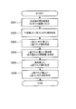
- FIG. 6 is a flowchart for explaining a manufacturing method of the laminated semiconductor wafer SW using the compound semiconductor substrate 40 as a starting material.
- the compound semiconductor substrate 40 is set in the MOCVD apparatus 1 shown in FIG. 1 (step 201). Specifically, each substrate 110 is set on each substrate holder 30 so that the base layer 130 faces outward, and each substrate holder 30 on which each substrate 110 is set is provided on the support 20. It arrange
- the n-type contact layer 140a is formed on the base layer 130 using the MOCVD apparatus 1 (step 202), the n-type cladding layer 140b is formed on the n-type contact layer 140a (step 203), and the n-type contact layer 140a is formed.
- the light emitting layers 150 that is, the barrier layers 150a and the well layers 150b are alternately formed on the cladding layer 140b (step 204), and the p-type cladding layer 160a is formed on the light-emitting layer 150 (step 205).
- a p-type contact layer 160b is formed on the layer 160a (step 206) to obtain a laminated semiconductor wafer SW.
- the n-type semiconductor layer 140 (n-type contact layer 140a and n-type cladding layer 140b), the light emitting layer 150 (barrier layer 150a and well layer 150b), and the p-type semiconductor layer 160 (p-type cladding layer 160a and p-type contact layer).
- the formation of 160b) is performed continuously. That is, by changing the composition of the organometallic gas MO supplied into the reaction vessel 10 in the course of forming the compound semiconductor layer 100, the composition is different without opening the lid 12 of the reaction vessel 10 halfway. A plurality of films can be continuously formed and stacked.
- the configuration of the compound semiconductor substrate 40 is not limited to this.
- the compound semiconductor substrate 40 may be configured by forming the n-type contact layer 140a on the base layer 130 and including the substrate 110, the intermediate layer 120, the base layer 130, and the n-type contact layer 140a.
- step 202 may be omitted in manufacturing the laminated semiconductor wafer SW.
- a transparent positive electrode 170 is laminated on the p-type semiconductor layer 160 of the laminated semiconductor wafer SW obtained by the process shown in FIG. 6, and a positive electrode bonding pad 180 is formed thereon. Further, an exposed region 140c is formed in the n-type contact layer 140a using etching or the like, and a negative electrode bonding pad 190 is provided in the exposed region 140c. Thereafter, the surface of the substrate 110 opposite to the surface on which the intermediate layer 120 is formed is ground and polished until a predetermined thickness is reached. Then, the light-emitting element chip LC is obtained by cutting the wafer with the adjusted thickness of the substrate 110 into, for example, a 350 ⁇ m square.
- the protective member 60 is arrange
- the MOCVD apparatus 1 power supply to the coil of the heating unit 50 is started, and the support 20 is electromagnetically heated by the current flowing through the heating unit 50. Further, when the support 20 is heated by electromagnetic induction, the six substrate holders 30 held by the support 20 and the compound semiconductor substrate 40 held by each substrate holder 30 are heated to a predetermined temperature. . Furthermore, supply of purge gas from the monitoring device 90 toward the reaction chamber is started.
- the MOCVD apparatus 1 supplies the organometallic gas MO and ammonia NH 3 for the n-type contact layer 140a from the supply pipe 13 to the reaction chamber by a gas supply mechanism (not shown). Accordingly, in the reaction chamber, the organic metal and ammonia NH 3 react in the vicinity of the heated compound semiconductor substrate 40, and as a result, a group III nitride compound for the n-type contact layer 140a is generated. Then, most of the generated group III nitride compound for the n-type contact layer 140a falls to the support 20 side located below the source gas supply port, and is held on the support 20 via the substrate holder 30. It adheres to the compound semiconductor substrate 40. At this time, since the compound semiconductor substrate 40 is heated to a predetermined temperature, the crystal of the group III nitride compound for the n-type contact layer 140a grows epitaxially on the base layer 130 of the compound semiconductor substrate 40.
- the MOCVD apparatus 1 uses an unillustrated gas supply mechanism to change the n-type cladding layer from the supply pipe 13 to the reaction chamber, instead of the metal-organic gas MO for the n-type contact layer 140a.
- An organometallic gas MO for 140b is supplied.
- the MOCVD apparatus 1 continues to supply ammonia NH 3 . Accordingly, in the reaction chamber, the organic metal and ammonia NH 3 react in the vicinity of the compound semiconductor substrate 40 to be heated, and as a result, a group III nitride compound for the n-type cladding layer 140b is generated.
- the n-type cladding layer 140b formed on the compound semiconductor substrate 40 includes a light emitting layer having a plurality of barrier layers 150a and a plurality of well layers 150b. 150, and a p-type semiconductor layer 160 having a p-type cladding layer 160a and a p-type contact layer 160b are sequentially formed. Through such a procedure, the laminated semiconductor wafer SW can be obtained.
- the base layer 130 is formed on the substrate 110 / intermediate layer 120 in advance using the MOCVD apparatus 1, and this is also the same procedure as described above.
- the underlayer 130 can be formed using
- a part of the group III nitride compound (reaction product) generated in the reaction chamber is not only the compound semiconductor substrate 40 but also the surface of the protective member 60, for example. Also adhere to. At this time, like the compound semiconductor layer 100 formed on the compound semiconductor substrate 40, a plurality of films having different compositions are stacked on the surface of the protective member 60.
- the surface of the protective member 60 faces the compound semiconductor substrate 40 held on the support 20 via the substrate holder 30 as described above, and above the crystal growth surface of the compound semiconductor substrate 40.
- the surface of the protective member 60 is located at the top.
- the protection member 60 is made of a material different from quartz glass, that is, a group III nitride compound semiconductor constituting the compound semiconductor layer 100.
- the group III nitride compound semiconductor film adhered and deposited on the surface of the protective member 60 may be peeled off from the protective member 60.
- the group III nitride compound semiconductor is peeled off from the protective member 60, there is a possibility that foreign matters generated by the peeling may fall on the compound semiconductor substrate 40 located below the protective member 60.
- each layer constituting the compound semiconductor layer 100 is further formed at the foreign matter attachment site.
- the obtained laminated semiconductor wafer SW As a result, in the obtained laminated semiconductor wafer SW, a portion to which foreign matter is attached cannot be used as the light emitting element chip LC, and the yield of the light emitting element chip LC is reduced accordingly. Further, if the number or amount of foreign matters adhering to the compound semiconductor substrate 40 is remarkably large, the laminated semiconductor wafer SW has to be discarded, and the yield of the laminated semiconductor wafer SW is reduced accordingly.
- the surface area of the protective member 60 is increased by forming a plurality of grooves 63 radially on the surface of the protective member 60, so that the surface of the protective member 60 is Peeling of the attached group III nitride compound semiconductor is suppressed.
- the adhesion and deposition of foreign matters on the compound semiconductor substrate 40 is suppressed.
- the yield of the laminated semiconductor wafer SW can be improved, and further, the yield of the light emitting element chips LC manufactured using the laminated semiconductor wafer SW as a starting material can also be improved.
- the protective member 60 is reused after removing the reaction product adhering to the surface.
- the reaction product attached to the surface of the protective member 60 can be easily scraped off with a brush or the like. . That is, the reaction product adhering to the surface of the protective member 60 can be removed by scraping radially along the groove 63 of the protective member 60 using a brush.
- a plurality of grooves 63 are formed radially on the surface of the protective member 60, so that the organometallic gas MO and ammonia NH 3 introduced into the reaction vessel 10 are supported radially. It can supply toward 20 side.
- the inventor forms the compound semiconductor layer 100 on the compound semiconductor substrate 40 using the MOCVD apparatus 1 shown in FIG. 1, and the configuration of the protective member 60 used at that time and the compound semiconductor layer 40 are formed on the compound semiconductor substrate 40.
- the relationship with the number of foreign substances existing in the compound semiconductor layer 100 was examined.
- the MOCVD apparatus 1 capable of mounting eight substrate holders 30, that is, eight compound semiconductor substrates 40 on the support 20 was used.
- the protective member 60 having a plurality of radial grooves 63 formed on the surface thereof as shown in FIG. 3 was used.
- Comparative Example 1 and Comparative Example 2 a protective member 60 having a flat surface was used.
- the flow rate per unit time of the purge gas supplied from the monitoring device 90 to the reaction chamber through the through holes provided in the lid portion 12 and the protective member 60 was set as before, In Example 2, considering the possibility that the reaction product attached to the surface of the protective member 60 was peeled off by the air flow of the purge gas, the flow rate of the purge gas per unit time was made smaller than before.
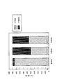
- the MOCVD apparatus 1 is used to perform the film forming operation 56 times under each condition, and the compound semiconductor layer 100 of the 448 (8 ⁇ 56) stacked semiconductor wafers SW obtained in each condition is visually observed.
- FIG. 7 is a diagram showing the evaluation results of Examples, Comparative Example 1 and Comparative Example 2.
- the vertical axis indicates the number of stacked semiconductor wafers SW, and indicates the number of acceptable products and unacceptable products in each of the example, comparative example 1, and comparative example 2.
- the vertical axis indicates the number of stacked semiconductor wafers SW, and indicates the number of acceptable products and unacceptable products in each of the example, comparative example 1, and comparative example 2.
- FIG. 7 in the example, only one rejected product was found out of 448 laminated semiconductor wafers SW, whereas in Comparative Example 1, 10 out of 448 failed products. In Comparative Example 2, 9 out of 448 sheets were rejected.
- the groove 63 which is a kind of unevenness is formed on the surface of the protection member 60 attached above the compound semiconductor substrate 40, that is, the surface facing the crystal growth surface of the compound semiconductor substrate 40, thereby protecting the surface. It is understood that peeling of the group III nitride compound semiconductor from the member 60 and the accompanying adhesion and deposition of foreign matter on the compound semiconductor substrate 40 are suppressed.
- the plurality of radial grooves 63 are formed on the surface of the protection member 60, but the present invention is not limited to this.
- FIG. 8 shows another configuration example of the surface of the protection member 60.
- a large number of irregularities having regularity or irregularity may be formed on the surface of the protective member 60, for example.
- a plurality of grooves 63 extending in one direction may be formed on the surface of the protection member 60.
- a plurality of grooves 63 directed in one direction and a plurality of other grooves 63 directed in a direction orthogonal to the one direction are formed on the surface of the protective member 60. Also good.
- a plurality of grooves 63 may be formed concentrically on the surface of the protective member 60. And as shown in FIG.8 (e), you may make it form the groove
- the source gas is supplied from the first through-hole 61 of the protective member 60 provided above the support 20, but the present invention is not limited to this. That is, the source gas may be supplied from the side of the support 20 in the horizontal direction.
- FIG. (A) is the figure which looked at the protection member from the lower side
- (b) is the figure which looked at the protection member from the upper side
- (C) is a figure which shows the cross section of a protection member.
- sectional drawing of the laminated semiconductor wafer manufactured using a MOCVD apparatus is an example of sectional drawing of the light emitting element chip
- FIG. (A)-(e) is a figure for demonstrating the other structural example of a protection member.
Landscapes
- Chemical & Material Sciences (AREA)
- General Chemical & Material Sciences (AREA)
- Chemical Kinetics & Catalysis (AREA)
- Engineering & Computer Science (AREA)
- Materials Engineering (AREA)
- Mechanical Engineering (AREA)
- Metallurgy (AREA)
- Organic Chemistry (AREA)
- Led Devices (AREA)
- Chemical Vapour Deposition (AREA)
Abstract
Description
。MOCVD法では、例えばIII族有機金属原料ガスおよびV族原料ガスを、高純度水素キャリアガスとの混合ガスとして反応室内に供給し、反応室内で加熱された基板の付近で原料を熱分解し、基板上に化合物半導体結晶をエピタキシャル成長させることで、化合物半導体ウェハを得ている。
このようにして付着、堆積した反応生成物は、基板に対しMOCVD法による化合物半導体の製膜を行った後、清掃を行うことによって除去される。
また、基板上に付着した反応生成物の数あるいは量が著しく多いと、化合物半導体層を形成した基板自体を破棄せざるを得なくなってしまうため、化合物半導体層を形成した基板の製造における歩留まりの低下を招いていた。
図1は本実施の形態が適用される化合物半導体製造装置の一例としてのMOCVD(Metal Organic Chemical Vapor Deposition)装置1の断面構成を示す図である。また、図2は、図1に示すMOCVD装置1のII-II断面図である。
このMOCVD装置1は、化合物半導体の結晶をエピタキシャル成長させるための基板110(後述する図4参照)やさらにその上に予め任意の組成の化合物半導体層を少なくとも1層形成してなる化合物半導体基板(一例として化合物半導体基板40も挙げられ、本明細書ではこれらを被形成体ともいう)を任意に選ぶことができ、例えば化合物半導体基板40を用いる場合には、その結晶成長面が上方を向くように配置し、且つ、エピタキシャル成長を行わせる結晶の原料となる原料ガスを、化合物半導体基板40の上方から供給する所謂縦型の構成を有している。
これらのうち、反応容器10は、円筒状の形状を有し上方に向かう開口が形成されるとともにその内部に支持体20を収容する収容部11と、円板状の形状を有しこの収容部11の上部に取り付けられる蓋部12とを備える。
一方、収容部11の底面には、反応室内に供給された原料ガスを反応室の外部に排出するための複数の排気管が貫通形成されている。さらに、収容部11の底面中央部には、後述する軸21を通すための貫通孔も形成されている。
本実施の形態では、MOCVD装置1を用いて基板110上に予め任意の組成の化合物半導体層を形成した化合物半導体基板40上に、さらにIII族窒化物半導体層を形成する。このため、原料として、III族の元素を含む有機金属と窒素を含むアンモニアNH3とを使用する。ただし、有機金属は主として液体原料であるため、液体状の有機金属に窒素N2および水素H2にてバブリングを行い、得られた窒素N2および水素H2および有機金属を混合させてなる有機金属ガスMOを原料ガスとして供給する。本実施の形態では、供給管13より有機金属ガスMOおよびアンモニアNH3の供給を行う。
また、n型のドーパントとしては、モノシラン(SiH4)やジシラン(Si2H6)Si原料、あるいは、ゲルマンガス(GeH4)やテトラメチルゲルマニウム((CH3)4Ge)やテトラエチルゲルマニウム((C2H5)4Ge)をGe原料として用いてもよい。一方、p型のドーパントとしては、例えばビスシクロペンタジエニルマグネシウム(Cp2Mg)またはビスエチルシクロペンタジエニルマグネシウム(EtCp2Mg)をMg原料として用いてもよい。さらに、アンモニアに代えて、ヒドラジン(N2H4)を用いることもできる。なお、上述した有機金属MO以外にも、他のIII属元素を含有させた構成とすることができ、必要に応じてGe、Si、Mg、Ca、Zn、Be等のドーパントを含有させることができる。さらに、意図的に添加した元素に限らず、成膜条件等に依存して必然的に含まれる不純物、並びに原料、反応管材質に含まれる微量不純物を含む場合もある。
なお、支持体20の内部には、支持体20に設けられた6個の凹部の底面に向けて窒素N2を供給するための貫通孔(図示せず)が形成されている。なお、支持体20に設けられた6個の凹部の底面に対する窒素N2の供給手法については、適宜設定変更して差し支えない。
そして、各基板保持体30は、それぞれが化合物半導体基板40を保持した状態で、上述した図示しない貫通孔を介して供給される窒素N2の流れにより、図2に示す矢印B方向に回転するようになっている。
基板110は、III族窒化物化合物半導体とは異なる材料から構成され、基板110上にIII族窒化物半導体結晶がエピタキシャル成長される。基板110を構成する材料としては、例えば、サファイア、炭化ケイ素(シリコンカーバイド:SiC)、シリコン、酸化亜鉛、酸化マグネシウム、酸化マンガン、酸化ジルコニウム、酸化マンガン亜鉛鉄、酸化マグネシウムアルミニウム、ホウ化ジルコニウム、酸化ガリウム、酸化インジウム、酸化リチウムガリウム、酸化リチウムアルミニウム、酸化ネオジウムガリウム、酸化ランタンストロンチウムアルミニウムタンタル、酸化ストロンチウムチタン、酸化チタン、ハフニウム、タングステン、モリブデン等が挙げられる。これらの中でも、サファイア、炭化ケイ素(シリコンカーバイド:SiC)が好ましい。
上述したように、基板110はIII族窒化物化合物半導体とは異なる材料から構成される。このため、図1に示すMOCVD装置1を用いて化合物半導体層100を成膜する前に、バッファ機能を発揮する中間層120を基板110上に設けておくことが好ましい。特に、中間層120が単結晶構造であることは、バッファ機能の面から好ましい。単結晶構造を有する中間層120を基板110上に成膜した場合、中間層120のバッファ機能が有効に作用し、中間層120上に成膜される下地層130と化合物半導体層100とは、良好な結晶性を持つ結晶膜となる。
中間層120は、Alを含有することが好ましく、III族窒化物であるAlNを含むことが特に好ましい。
下地層130に用いる材料としては、Gaを含むIII族窒化物(GaN系化合物半導体)が用いられ、特に、AlGaN、又はGaNを好適に用いることができる。下地層130の膜厚は0.1μm以上、好ましくは0.5μm以上、さらに好ましくは1μm以上である。
n型半導体層140は、n型コンタクト層140aおよびn型クラッド層140bから構成される。
ここで、n型コンタクト層140aとしては、下地層130と同様にGaN系化合物半導体が用いられる。また、下地層130およびn型コンタクト層140aを構成する窒化ガリウム系化合物半導体は同一組成であることが好ましく、これらの合計の膜厚を0.1μm~20μm、好ましくは0.5μm~15μm、さらに好ましくは1μm~12μmの範囲に設定することが好ましい。
発光層150は、窒化ガリウム系化合物半導体からなる障壁層150aと、インジウムを含有する窒化ガリウム系化合物半導体からなる井戸層150bとが交互に繰り返して積層され、且つ、n型半導体層140側及びp型半導体層160側にそれぞれ障壁層150aが配される順で積層して形成される。本実施の形態において、発光層150は、6層の障壁層150aと5層の井戸層150bとが交互に繰り返して積層され、発光層150の最上層及び最下層に障壁層150aが配され、各障壁層150a間に井戸層150bが配される構成となっている。
また、井戸層150bには、インジウムを含有する窒化ガリウム系化合物半導体として、例えば、Ga1-sInsN(0<s<0.4)等の窒化ガリウムインジウムを用いることができる。
発光層150全体の膜厚としては、特に限定されないが、量子効果の得られる程度の膜厚、即ち臨界膜厚領域であることが好ましい。例えば、発光層150の膜厚は、1nm~500nmの範囲であることが好ましく、100nm前後の膜厚であればより好ましい。また、井戸層150bの膜厚としては、特に限定されないが、量子効果の得られる程度の膜厚であることが好ましい。
p型半導体層160は、p型クラッド層160aおよびp型コンタクト層160bから構成される。p型クラッド層160aとしては、好ましくは、AldGa1-dN(0<d≦0.4)のものが挙げられる。p型クラッド層160aの膜厚は、好ましくは1nm~400nmであり、より好ましくは5nm~100nmである。
一方、p型コンタクト層160bとしては、AleGa1-eN(0≦e<0.5)を含んでなる窒化ガリウム系化合物半導体層が挙げられる。p型コンタクト層160bの膜厚は、特に限定されないが、10nm~500nmが好ましく、より好ましくは50nm~200nmである。
発光素子チップLCにおいては、p型半導体層160のp型コンタクト層160b上に透明正極170が積層され、さらにその上に正極ボンディングパッド180が形成されるとともに、n型半導体層140のn型コンタクト層140aに形成された露出領域140cに負極ボンディングパッド190が積層されている。
透明正極170を構成する材料としては、例えば、ITO(In2O3-SnO2)、AZO(ZnO-Al2O3)、IZO(In2O3-ZnO)、GZO(ZnO-Ga2O3)等の従来公知の材料が挙げられる。また、透明正極170の構造は特に限定されず、従来公知の構造を採用することができる。透明正極170は、p型半導体層160上のほぼ全面を覆うように形成しても良く、格子状や樹形状に形成しても良い。
透明正極170上に形成される電極としての正極ボンディングパッド180は、例えば、従来公知のAu、Al、Ti、V、Cr、Mn、Co、Zn、Ge、Zr、Nb、Mo、Ru、Ta、Ni、Cu等の材料から構成される。正極ボンディングパッド180の構造は特に限定されず、従来公知の構造を採用することができる。
正極ボンディングパッド180の厚さは、例えば100nm~2000nmの範囲内であり、好ましくは300nm~1000nmの範囲内である。
負極ボンディングパッド190は、基板110上に成膜された中間層120および下地層130の上にさらに成膜された化合物半導体層100(n型半導体層140、発光層150およびp型半導体層160)において、n型半導体層140のn型コンタクト層140aに接するように形成される。このため、負極ボンディングパッド190を形成する際は、p型半導体層160、発光層150およびn型半導体層140の一部を除去し、n型コンタクト層140aの露出領域140cを形成し、この上に負極ボンディングパッド190を形成する。
負極ボンディングパッド190の材料としては、正極ボンディングパッド180と同じ組成・構造でもよく、各種組成および構造の負極が周知であり、これら周知の負極を何ら制限無く用いることができ、この技術分野でよく知られた慣用の手段で設けることができる。
まず、所定の直径と厚さとを有するサファイア製の基板110を、図示しないスパッタリング装置にセットする。そして、スパッタリング装置にて、基板110上に、V族元素を含むガスと金属材料とをプラズマで活性化して反応させることにより、III族窒化物からなる中間層120を形成する。
続いて、中間層120が形成された基板110を、図1に示すMOCVD装置1にセットする。具体的に説明すると、中間層120が外側に向かうように、各基板110を各基板保持体30にセットし、各基板110がセットされた各基板保持体30を、支持体20に設けられた各凹部に、中間層120が上方を向くように配置する。そして、MOCVD装置1を用いて中間層120の上に下地層130の形成を行い、化合物半導体基板40を得る。
図6は、化合物半導体基板40を出発材料とする積層半導体ウェハSWの製造方法を説明するためのフローチャートである。
化合物半導体基板40を、図1に示すMOCVD装置1にセットする(ステップ201)。具体的に説明すると、下地層130が外側に向かうように、各基板110を各基板保持体30にセットし、各基板110がセットされた各基板保持体30を、支持体20に設けられた各凹部に、中間層120が上方を向くように配置する。そして、MOCVD装置1を用いて下地層130の上にn型コンタクト層140aを形成し(ステップ202)、n型コンタクト層140aの上にn型クラッド層140bを形成し(ステップ203)、n型クラッド層140bの上に発光層150すなわち障壁層150aと井戸層150bとを交互に形成し(ステップ204)、発光層150の上にp型クラッド層160aを形成し(ステップ205)、p型クラッド層160aの上にp型コンタクト層160bを形成し(ステップ206)、積層半導体ウェハSWを得る。
図6に示すプロセスによって得られた積層半導体ウェハSWのp型半導体層160上に透明正極170を積層し、その上に正極ボンディングパッド180を形成する。また、エッチング等を用いてn型コンタクト層140aに露出領域140cを形成し、この露出領域140cに負極ボンディングパッド190を設ける。
その後、基板110の中間層120の形成面とは反対の面を、所定の厚さになるまで研削及び研磨する。
そして、基板110の厚さが調整されたウェハを、例えば350μm角の正方形に切断することにより、発光素子チップLCを得る。
まず初めに、6枚の基板保持体30の凹部に、それぞれ1枚ずつ化合物半導体基板40をセットする。このとき、化合物半導体基板40の下地層130を外部に露出させるようにする。続いて、反応容器10の蓋部12を開け、それぞれに化合物半導体基板40がセットされた6枚の基板保持体30を、MOCVD装置1の支持体20に設けられた6個の凹部にセットする。このとき、化合物半導体基板40の下地層130が上方を向くようにする。
その後、保護部材60が取り付けられた蓋部12を閉じて収容部11と蓋部12とを密着させる。
本発明者は、図1に示すMOCVD装置1を用いて化合物半導体基板40上に化合物半導体層100の形成を行い、そのときに使用した保護部材60の構成と化合物半導体基板40上に形成された化合物半導体層100内に存在する異物の数との関係について検討を行った。ただし、ここでは、支持体20上に8枚の基板保持体30すなわち8枚の化合物半導体基板40を搭載できるMOCVD装置1を用いた。
図7において、縦軸は積層半導体ウェハSWの枚数を示しており、実施例、比較例1および比較例2のそれぞれにおける合格品、不合格品の数を示している。
図7より明らかなように、実施例においては、448枚の積層半導体ウェハSWのうち不合格品が1枚だけであったのに対し、比較例1では448枚のうち10枚が不合格品となり、比較例2では448枚のうち9枚が不合格品となった。
図8は、保護部材60の表面の他の構成例を示している。
まず、図8(a)に示すように、保護部材60の表面に、例えば規則性あるいは不規則性を有する多数の凹凸を形成するようにしてもよい。
また、図8(b)に示すように、保護部材60の表面に、一方向に向かう複数の溝63を形成するようにしてもよい。
さらに、図8(c)に示すように、保護部材60の表面に、一方向に向かう複数の溝63およびこの一方向と直交する方向に向かう他の複数の溝63とを形成するようにしてもよい。
さらにまた、図8(d)に示すように、保護部材60の表面に、同心円状に複数の溝63を形成するようにしてもよい。
そして、図8(e)に示すように、保護部材60の表面に、同心円状ではなく渦巻き状に溝63を形成するようにしてもよい。なお、図8(e)では、1本の溝63を渦巻き状に形成する例を示しているが、複数の溝63を渦巻き状に形成するものであってもよい。
Claims (12)
- 有機金属気相成長法を用いて化合物半導体の層を形成する化合物半導体製造装置であって、
反応容器と、
外部から前記反応容器内に前記化合物半導体の原料ガスを供給する原料供給口と、
前記反応容器内に配置され、被形成体の被形成面が上方を向くように当該被形成体を支持する支持体と、
前記支持体に支持された前記被形成体の上方に配置され、前記被形成面と対向する対向面に凹凸が形成される対向部材と
を有することを特徴とする化合物半導体製造装置。 - 前記対向部材の前記対向面には、連続性を有する凹部からなる溝が形成されることを特徴とする請求項1記載の化合物半導体製造装置。
- 前記原料供給口が前記対向部材に設けられた貫通孔にて構成され、
前記対向部材の前記対向面には、前記貫通孔を中心として内側から外側に向かう前記溝が形成されることを特徴とする請求項2記載の化合物半導体製造装置。 - 前記溝が、前記貫通孔を中心として放射状に複数形成されることを特徴とする請求項3記載の化合物半導体製造装置。
- 有機金属気相成長法を用いて化合物半導体の層を被形成体の被形成面に形成する化合物半導体の製造方法であって、
前記被形成面が上方を向くように反応容器内に前記被形成体を取り付け、
前記被形成体の上方に前記被形成面と対向する対向面に凹凸が形成された対向部材を配置し、
前記反応容器内に前記化合物半導体の原料ガスを供給すること
を特徴とする化合物半導体の製造方法。 - 前記対向面には、連続性を有する溝が形成されることを特徴とする請求項5記載の化合物半導体の製造方法。
- 前記対向部材に設けられた貫通孔を介して前記反応容器内に前記原料ガスを供給し、
前記対向面には、前記貫通孔を中心として内側から外側に向かう前記溝が形成されることを特徴とする請求項6記載の化合物半導体の製造方法。 - 前記対向面には、前記貫通孔を中心として放射状に複数の前記溝が形成されることを特徴とする請求項7記載の化合物半導体の製造方法。
- 有機金属気相成長法を用いて化合物半導体の層を形成する化合物半導体製造装置で用いられる化合物半導体製造用治具であって、
凹凸を有し被形成面が上方を向くように配置される被形成体の上方に対向する対向面と、
前記対向面と当該対向面の裏面とを貫通するように形成され、前記被形成体の上方から当該被形成体に前記化合物半導体の原料ガスを供給する原料供給口と
を有することを特徴とする化合物半導体製造用治具。 - 前記対向面には、連続性を有する溝が形成されることを特徴とする請求項9記載の化合物半導体製造用治具。
- 前記対向面には、前記原料供給口を中心として内側から外側に向かう前記溝が形成されることを特徴とする請求項10記載の化合物半導体製造用治具。
- 前記溝が、前記原料供給口を中心として放射状に複数形成されていることを特徴とする請求項11記載の化合物半導体製造用治具。
Priority Applications (4)
| Application Number | Priority Date | Filing Date | Title |
|---|---|---|---|
| CN200980143008.0A CN102197460B (zh) | 2008-11-05 | 2009-11-04 | 化合物半导体制造装置、化合物半导体制造方法以及化合物半导体制造用型架 |
| KR1020117004936A KR101253423B1 (ko) | 2008-11-05 | 2009-11-04 | 화합물 반도체 제조 장치, 화합물 반도체의 제조 방법, 및 화합물 반도체 제조용 지그 |
| DE112009002396.7T DE112009002396B4 (de) | 2008-11-05 | 2009-11-04 | Vorrichtung zum Herstellen eines Verbindungshalbleiters, Verfahren zum Herstellen eines Verbindungshalbleiters und Einspannvorrichtung zum Herstellen eines Verbindungshalbleiters |
| US13/126,110 US8591656B2 (en) | 2008-11-05 | 2009-11-04 | Compound semiconductor manufacturing device, compound semiconductor manufacturing method, and jig for manufacturing compound semiconductor |
Applications Claiming Priority (2)
| Application Number | Priority Date | Filing Date | Title |
|---|---|---|---|
| JP2008284349A JP5453768B2 (ja) | 2008-11-05 | 2008-11-05 | 化合物半導体製造装置、化合物半導体の製造方法、および化合物半導体製造用治具 |
| JP2008-284349 | 2008-11-05 |
Publications (1)
| Publication Number | Publication Date |
|---|---|
| WO2010053094A1 true WO2010053094A1 (ja) | 2010-05-14 |
Family
ID=42152902
Family Applications (1)
| Application Number | Title | Priority Date | Filing Date |
|---|---|---|---|
| PCT/JP2009/068834 Ceased WO2010053094A1 (ja) | 2008-11-05 | 2009-11-04 | 化合物半導体製造装置、化合物半導体の製造方法、および化合物半導体製造用治具 |
Country Status (7)
| Country | Link |
|---|---|
| US (1) | US8591656B2 (ja) |
| JP (1) | JP5453768B2 (ja) |
| KR (1) | KR101253423B1 (ja) |
| CN (1) | CN102197460B (ja) |
| DE (1) | DE112009002396B4 (ja) |
| TW (1) | TWI506678B (ja) |
| WO (1) | WO2010053094A1 (ja) |
Cited By (3)
| Publication number | Priority date | Publication date | Assignee | Title |
|---|---|---|---|---|
| JP2013038153A (ja) * | 2011-08-05 | 2013-02-21 | Showa Denko Kk | エピタキシャルウェハの製造装置及び製造方法 |
| JP2013038152A (ja) * | 2011-08-05 | 2013-02-21 | Showa Denko Kk | エピタキシャルウェハの製造装置及び製造方法 |
| CN115786873A (zh) * | 2022-12-05 | 2023-03-14 | 英诺赛科(珠海)科技有限公司 | 半导体制造设备、腔体总成、及成长iii族氮化物的方法 |
Families Citing this family (16)
| Publication number | Priority date | Publication date | Assignee | Title |
|---|---|---|---|---|
| JP5272390B2 (ja) * | 2007-11-29 | 2013-08-28 | 豊田合成株式会社 | Iii族窒化物半導体の製造方法、iii族窒化物半導体発光素子の製造方法、及びiii族窒化物半導体発光素子、並びにランプ |
| US8535445B2 (en) * | 2010-08-13 | 2013-09-17 | Veeco Instruments Inc. | Enhanced wafer carrier |
| TWI654666B (zh) | 2014-01-27 | 2019-03-21 | Veeco Instruments, Inc. | 用於化學氣相沉積系統之具有複合半徑容置腔的晶圓載具 |
| JP6229609B2 (ja) * | 2014-07-18 | 2017-11-15 | 豊田合成株式会社 | Iii族窒化物半導体発光素子の製造方法 |
| JP6382629B2 (ja) * | 2014-08-07 | 2018-08-29 | 大陽日酸株式会社 | 気相成長装置 |
| WO2016084492A1 (ja) * | 2014-11-26 | 2016-06-02 | 日本碍子株式会社 | 13族元素窒化物結晶の製造方法および装置 |
| JP2016157734A (ja) * | 2015-02-23 | 2016-09-01 | 豊田合成株式会社 | Iii族窒化物半導体発光素子の製造方法 |
| CN107326343B (zh) * | 2017-08-22 | 2020-05-12 | 中国科学院半导体研究所 | 用于薄膜材料生长的感应加热装置 |
| CN107475691B (zh) * | 2017-08-24 | 2020-07-07 | 中国科学院半导体研究所 | 一种基于电磁感应的加热装置 |
| JP2019079867A (ja) * | 2017-10-20 | 2019-05-23 | 漢民科技股▲分▼有限公司 | 気相成膜装置 |
| CN109688651A (zh) * | 2018-12-27 | 2019-04-26 | 东营源纳合金科技有限公司 | 一种不规则合金坯料加热装置及其加热方法 |
| JP7477515B2 (ja) * | 2019-01-08 | 2024-05-01 | アプライド マテリアルズ インコーポレイテッド | 基板処理チャンバ用のポンピング装置及び方法 |
| JP7413941B2 (ja) * | 2020-07-03 | 2024-01-16 | 信越半導体株式会社 | 接合型半導体素子及び接合型半導体素子の製造方法 |
| JP7354943B2 (ja) | 2020-07-03 | 2023-10-03 | 信越半導体株式会社 | 接合型半導体受光素子及び接合型半導体受光素子の製造方法 |
| CN116949424B (zh) * | 2023-07-28 | 2025-08-15 | 长鑫科技集团股份有限公司 | 衬底处理装置及其镀膜挡件 |
| TWI897069B (zh) * | 2023-10-20 | 2025-09-11 | 台亞半導體股份有限公司 | 頂板及含有頂板之磊晶成長裝置 |
Citations (5)
| Publication number | Priority date | Publication date | Assignee | Title |
|---|---|---|---|---|
| JPH10163180A (ja) * | 1996-10-02 | 1998-06-19 | Matsushita Electron Corp | 電子デバイスの製造装置及び電子デバイスの製造方法 |
| JP2000228398A (ja) * | 1998-11-30 | 2000-08-15 | Kawasaki Steel Corp | 処理装置、これを用いる付着物の剥離防止方法および半導体装置の製造方法、半導体製造装置の構成部品ならびにフォーカスリング |
| JP2002234793A (ja) * | 2001-02-07 | 2002-08-23 | Sony Corp | 半導体製造装置 |
| JP2003518199A (ja) * | 1999-12-22 | 2003-06-03 | アイクストロン、アーゲー | 化学気相成膜反応室及びそのための処理室 |
| JP2008247639A (ja) * | 2007-03-29 | 2008-10-16 | Tosoh Quartz Corp | 石英ガラス材料及びその製造方法 |
Family Cites Families (4)
| Publication number | Priority date | Publication date | Assignee | Title |
|---|---|---|---|---|
| US6007673A (en) * | 1996-10-02 | 1999-12-28 | Matsushita Electronics Corporation | Apparatus and method of producing an electronic device |
| JP3540936B2 (ja) * | 1998-03-31 | 2004-07-07 | 京セラ株式会社 | 真空容器 |
| US6447853B1 (en) * | 1998-11-30 | 2002-09-10 | Kawasaki Microelectronics, Inc. | Method and apparatus for processing semiconductor substrates |
| US20030124842A1 (en) | 2001-12-27 | 2003-07-03 | Applied Materials, Inc. | Dual-gas delivery system for chemical vapor deposition processes |
-
2008
- 2008-11-05 JP JP2008284349A patent/JP5453768B2/ja active Active
-
2009
- 2009-11-04 CN CN200980143008.0A patent/CN102197460B/zh active Active
- 2009-11-04 US US13/126,110 patent/US8591656B2/en active Active
- 2009-11-04 DE DE112009002396.7T patent/DE112009002396B4/de active Active
- 2009-11-04 KR KR1020117004936A patent/KR101253423B1/ko active Active
- 2009-11-04 WO PCT/JP2009/068834 patent/WO2010053094A1/ja not_active Ceased
- 2009-11-05 TW TW098137611A patent/TWI506678B/zh active
Patent Citations (5)
| Publication number | Priority date | Publication date | Assignee | Title |
|---|---|---|---|---|
| JPH10163180A (ja) * | 1996-10-02 | 1998-06-19 | Matsushita Electron Corp | 電子デバイスの製造装置及び電子デバイスの製造方法 |
| JP2000228398A (ja) * | 1998-11-30 | 2000-08-15 | Kawasaki Steel Corp | 処理装置、これを用いる付着物の剥離防止方法および半導体装置の製造方法、半導体製造装置の構成部品ならびにフォーカスリング |
| JP2003518199A (ja) * | 1999-12-22 | 2003-06-03 | アイクストロン、アーゲー | 化学気相成膜反応室及びそのための処理室 |
| JP2002234793A (ja) * | 2001-02-07 | 2002-08-23 | Sony Corp | 半導体製造装置 |
| JP2008247639A (ja) * | 2007-03-29 | 2008-10-16 | Tosoh Quartz Corp | 石英ガラス材料及びその製造方法 |
Cited By (8)
| Publication number | Priority date | Publication date | Assignee | Title |
|---|---|---|---|---|
| JP2013038153A (ja) * | 2011-08-05 | 2013-02-21 | Showa Denko Kk | エピタキシャルウェハの製造装置及び製造方法 |
| JP2013038152A (ja) * | 2011-08-05 | 2013-02-21 | Showa Denko Kk | エピタキシャルウェハの製造装置及び製造方法 |
| EP2741316A4 (en) * | 2011-08-05 | 2015-03-11 | Showa Denko Kk | DEVICE FOR MANUFACTURING EPITAXIAL WAFER AND METHOD OF MANUFACTURE |
| EP2741317A4 (en) * | 2011-08-05 | 2015-03-18 | Showa Denko Kk | DEVICE AND METHOD FOR PRODUCING AN EPITAXIAL DISC |
| US9607832B2 (en) | 2011-08-05 | 2017-03-28 | Showa Denko K.K. | Epitaxial wafer manufacturing device and manufacturing method |
| US9624602B2 (en) | 2011-08-05 | 2017-04-18 | Showa Denko K.K. | Epitaxial wafer manufacturing device and manufacturing method |
| CN115786873A (zh) * | 2022-12-05 | 2023-03-14 | 英诺赛科(珠海)科技有限公司 | 半导体制造设备、腔体总成、及成长iii族氮化物的方法 |
| CN115786873B (zh) * | 2022-12-05 | 2023-12-26 | 英诺赛科(珠海)科技有限公司 | 半导体制造设备、腔体总成、及成长iii族氮化物的方法 |
Also Published As
| Publication number | Publication date |
|---|---|
| TWI506678B (zh) | 2015-11-01 |
| DE112009002396T5 (de) | 2011-07-21 |
| CN102197460A (zh) | 2011-09-21 |
| DE112009002396B4 (de) | 2022-02-03 |
| CN102197460B (zh) | 2014-07-23 |
| JP5453768B2 (ja) | 2014-03-26 |
| US20110207299A1 (en) | 2011-08-25 |
| TW201027598A (en) | 2010-07-16 |
| US8591656B2 (en) | 2013-11-26 |
| KR20110033954A (ko) | 2011-04-01 |
| JP2010114203A (ja) | 2010-05-20 |
| KR101253423B1 (ko) | 2013-04-11 |
Similar Documents
| Publication | Publication Date | Title |
|---|---|---|
| JP5453768B2 (ja) | 化合物半導体製造装置、化合物半導体の製造方法、および化合物半導体製造用治具 | |
| JP5359698B2 (ja) | 化合物半導体の製造装置、化合物半導体の製造方法及び化合物半導体 | |
| JP5644256B2 (ja) | 化合物半導体の製造装置及び化合物半導体の製造方法 | |
| EP2770545B1 (en) | Growth substrate, nitride semiconductor device and method of manufacturing the same | |
| JP5904101B2 (ja) | 化合物半導体の製造装置およびウェハ保持体 | |
| WO2008041586A1 (fr) | Procédé de fabrication de dispositif semiconducteur émetteur de lumière à composé de nitrure de groupe iii, ce dispositif et lampe associée | |
| JP5440109B2 (ja) | 化合物半導体の製造方法 | |
| KR100956221B1 (ko) | 화학 기상 증착 장치용 서셉터 | |
| US7867801B2 (en) | Apparatus for producing group-III nitride semiconductor layer, method of producing group-III nitride semiconductor layer, method of producing group-III nitride semiconductor light-emitting device, group-III nitride semiconductor light-emitting device thereof, and lamp thereof | |
| JP5440114B2 (ja) | Iii族窒化物半導体の製造方法 | |
| JP5267262B2 (ja) | 化合物半導体の製造方法、化合物半導体発光素子の製造方法、化合物半導体製造装置 | |
| JP2013010681A (ja) | 窒化ガリウム基板、発光素子、電界効果トランジスタ及びエピタキシャル膜の製造方法 | |
| WO2012111884A1 (en) | Laminate substrate and method of fabricating the same | |
| JP2008243948A (ja) | エピタキシャル基板の製造方法 | |
| JP5046182B2 (ja) | 化合物半導体エピタキシャルウェーハの製造方法 | |
| JP2014120658A (ja) | 化合物半導体の成膜装置 | |
| JP2007042899A (ja) | 気相成長装置 | |
| JP2013035696A (ja) | Iii族窒化物半導体単結晶の製造方法 | |
| JP2011049309A (ja) | 化合物半導体の製造方法 |
Legal Events
| Date | Code | Title | Description |
|---|---|---|---|
| WWE | Wipo information: entry into national phase |
Ref document number: 200980143008.0 Country of ref document: CN |
|
| 121 | Ep: the epo has been informed by wipo that ep was designated in this application |
Ref document number: 09824793 Country of ref document: EP Kind code of ref document: A1 |
|
| ENP | Entry into the national phase |
Ref document number: 20117004936 Country of ref document: KR Kind code of ref document: A |
|
| WWE | Wipo information: entry into national phase |
Ref document number: 1120090023967 Country of ref document: DE |
|
| WWE | Wipo information: entry into national phase |
Ref document number: 13126110 Country of ref document: US |
|
| 122 | Ep: pct application non-entry in european phase |
Ref document number: 09824793 Country of ref document: EP Kind code of ref document: A1 |