WO2010052954A1 - アクティブマトリクス基板、アクティブマトリクス基板の製造方法、液晶パネル、液晶パネルの製造方法、液晶表示装置、液晶表示ユニット、テレビジョン受像機 - Google Patents
アクティブマトリクス基板、アクティブマトリクス基板の製造方法、液晶パネル、液晶パネルの製造方法、液晶表示装置、液晶表示ユニット、テレビジョン受像機 Download PDFInfo
- Publication number
- WO2010052954A1 WO2010052954A1 PCT/JP2009/062546 JP2009062546W WO2010052954A1 WO 2010052954 A1 WO2010052954 A1 WO 2010052954A1 JP 2009062546 W JP2009062546 W JP 2009062546W WO 2010052954 A1 WO2010052954 A1 WO 2010052954A1
- Authority
- WO
- WIPO (PCT)
- Prior art keywords
- electrode
- pixel
- pixel electrode
- capacitor
- conductor
- Prior art date
Links
Images


Classifications
-
- G—PHYSICS
- G02—OPTICS
- G02F—OPTICAL DEVICES OR ARRANGEMENTS FOR THE CONTROL OF LIGHT BY MODIFICATION OF THE OPTICAL PROPERTIES OF THE MEDIA OF THE ELEMENTS INVOLVED THEREIN; NON-LINEAR OPTICS; FREQUENCY-CHANGING OF LIGHT; OPTICAL LOGIC ELEMENTS; OPTICAL ANALOGUE/DIGITAL CONVERTERS
- G02F1/00—Devices or arrangements for the control of the intensity, colour, phase, polarisation or direction of light arriving from an independent light source, e.g. switching, gating or modulating; Non-linear optics
- G02F1/01—Devices or arrangements for the control of the intensity, colour, phase, polarisation or direction of light arriving from an independent light source, e.g. switching, gating or modulating; Non-linear optics for the control of the intensity, phase, polarisation or colour
- G02F1/13—Devices or arrangements for the control of the intensity, colour, phase, polarisation or direction of light arriving from an independent light source, e.g. switching, gating or modulating; Non-linear optics for the control of the intensity, phase, polarisation or colour based on liquid crystals, e.g. single liquid crystal display cells
- G02F1/133—Constructional arrangements; Operation of liquid crystal cells; Circuit arrangements
- G02F1/136—Liquid crystal cells structurally associated with a semi-conducting layer or substrate, e.g. cells forming part of an integrated circuit
- G02F1/1362—Active matrix addressed cells
- G02F1/136213—Storage capacitors associated with the pixel electrode
-
- G—PHYSICS
- G02—OPTICS
- G02F—OPTICAL DEVICES OR ARRANGEMENTS FOR THE CONTROL OF LIGHT BY MODIFICATION OF THE OPTICAL PROPERTIES OF THE MEDIA OF THE ELEMENTS INVOLVED THEREIN; NON-LINEAR OPTICS; FREQUENCY-CHANGING OF LIGHT; OPTICAL LOGIC ELEMENTS; OPTICAL ANALOGUE/DIGITAL CONVERTERS
- G02F1/00—Devices or arrangements for the control of the intensity, colour, phase, polarisation or direction of light arriving from an independent light source, e.g. switching, gating or modulating; Non-linear optics
- G02F1/01—Devices or arrangements for the control of the intensity, colour, phase, polarisation or direction of light arriving from an independent light source, e.g. switching, gating or modulating; Non-linear optics for the control of the intensity, phase, polarisation or colour
- G02F1/13—Devices or arrangements for the control of the intensity, colour, phase, polarisation or direction of light arriving from an independent light source, e.g. switching, gating or modulating; Non-linear optics for the control of the intensity, phase, polarisation or colour based on liquid crystals, e.g. single liquid crystal display cells
- G02F1/133—Constructional arrangements; Operation of liquid crystal cells; Circuit arrangements
- G02F1/136—Liquid crystal cells structurally associated with a semi-conducting layer or substrate, e.g. cells forming part of an integrated circuit
- G02F1/1362—Active matrix addressed cells
- G02F1/136259—Repairing; Defects
-
- G—PHYSICS
- G09—EDUCATION; CRYPTOGRAPHY; DISPLAY; ADVERTISING; SEALS
- G09G—ARRANGEMENTS OR CIRCUITS FOR CONTROL OF INDICATING DEVICES USING STATIC MEANS TO PRESENT VARIABLE INFORMATION
- G09G3/00—Control arrangements or circuits, of interest only in connection with visual indicators other than cathode-ray tubes
- G09G3/20—Control arrangements or circuits, of interest only in connection with visual indicators other than cathode-ray tubes for presentation of an assembly of a number of characters, e.g. a page, by composing the assembly by combination of individual elements arranged in a matrix no fixed position being assigned to or needed to be assigned to the individual characters or partial characters
- G09G3/34—Control arrangements or circuits, of interest only in connection with visual indicators other than cathode-ray tubes for presentation of an assembly of a number of characters, e.g. a page, by composing the assembly by combination of individual elements arranged in a matrix no fixed position being assigned to or needed to be assigned to the individual characters or partial characters by control of light from an independent source
- G09G3/36—Control arrangements or circuits, of interest only in connection with visual indicators other than cathode-ray tubes for presentation of an assembly of a number of characters, e.g. a page, by composing the assembly by combination of individual elements arranged in a matrix no fixed position being assigned to or needed to be assigned to the individual characters or partial characters by control of light from an independent source using liquid crystals
- G09G3/3611—Control of matrices with row and column drivers
- G09G3/3648—Control of matrices with row and column drivers using an active matrix
-
- G—PHYSICS
- G02—OPTICS
- G02F—OPTICAL DEVICES OR ARRANGEMENTS FOR THE CONTROL OF LIGHT BY MODIFICATION OF THE OPTICAL PROPERTIES OF THE MEDIA OF THE ELEMENTS INVOLVED THEREIN; NON-LINEAR OPTICS; FREQUENCY-CHANGING OF LIGHT; OPTICAL LOGIC ELEMENTS; OPTICAL ANALOGUE/DIGITAL CONVERTERS
- G02F1/00—Devices or arrangements for the control of the intensity, colour, phase, polarisation or direction of light arriving from an independent light source, e.g. switching, gating or modulating; Non-linear optics
- G02F1/01—Devices or arrangements for the control of the intensity, colour, phase, polarisation or direction of light arriving from an independent light source, e.g. switching, gating or modulating; Non-linear optics for the control of the intensity, phase, polarisation or colour
- G02F1/13—Devices or arrangements for the control of the intensity, colour, phase, polarisation or direction of light arriving from an independent light source, e.g. switching, gating or modulating; Non-linear optics for the control of the intensity, phase, polarisation or colour based on liquid crystals, e.g. single liquid crystal display cells
- G02F1/133—Constructional arrangements; Operation of liquid crystal cells; Circuit arrangements
- G02F1/1333—Constructional arrangements; Manufacturing methods
- G02F1/1343—Electrodes
- G02F1/134309—Electrodes characterised by their geometrical arrangement
- G02F1/134345—Subdivided pixels, e.g. for grey scale or redundancy
- G02F1/134354—Subdivided pixels, e.g. for grey scale or redundancy the sub-pixels being capacitively coupled
-
- G—PHYSICS
- G09—EDUCATION; CRYPTOGRAPHY; DISPLAY; ADVERTISING; SEALS
- G09G—ARRANGEMENTS OR CIRCUITS FOR CONTROL OF INDICATING DEVICES USING STATIC MEANS TO PRESENT VARIABLE INFORMATION
- G09G2300/00—Aspects of the constitution of display devices
- G09G2300/04—Structural and physical details of display devices
- G09G2300/0421—Structural details of the set of electrodes
- G09G2300/0426—Layout of electrodes and connections
-
- G—PHYSICS
- G09—EDUCATION; CRYPTOGRAPHY; DISPLAY; ADVERTISING; SEALS
- G09G—ARRANGEMENTS OR CIRCUITS FOR CONTROL OF INDICATING DEVICES USING STATIC MEANS TO PRESENT VARIABLE INFORMATION
- G09G2300/00—Aspects of the constitution of display devices
- G09G2300/04—Structural and physical details of display devices
- G09G2300/0439—Pixel structures
- G09G2300/0443—Pixel structures with several sub-pixels for the same colour in a pixel, not specifically used to display gradations
- G09G2300/0447—Pixel structures with several sub-pixels for the same colour in a pixel, not specifically used to display gradations for multi-domain technique to improve the viewing angle in a liquid crystal display, such as multi-vertical alignment [MVA]
-
- G—PHYSICS
- G09—EDUCATION; CRYPTOGRAPHY; DISPLAY; ADVERTISING; SEALS
- G09G—ARRANGEMENTS OR CIRCUITS FOR CONTROL OF INDICATING DEVICES USING STATIC MEANS TO PRESENT VARIABLE INFORMATION
- G09G2300/00—Aspects of the constitution of display devices
- G09G2300/08—Active matrix structure, i.e. with use of active elements, inclusive of non-linear two terminal elements, in the pixels together with light emitting or modulating elements
- G09G2300/0876—Supplementary capacities in pixels having special driving circuits and electrodes instead of being connected to common electrode or ground; Use of additional capacitively coupled compensation electrodes
-
- G—PHYSICS
- G09—EDUCATION; CRYPTOGRAPHY; DISPLAY; ADVERTISING; SEALS
- G09G—ARRANGEMENTS OR CIRCUITS FOR CONTROL OF INDICATING DEVICES USING STATIC MEANS TO PRESENT VARIABLE INFORMATION
- G09G2330/00—Aspects of power supply; Aspects of display protection and defect management
- G09G2330/08—Fault-tolerant or redundant circuits, or circuits in which repair of defects is prepared
Definitions
- the present invention relates to an active matrix substrate in which a plurality of pixel electrodes are provided in one pixel region, and a liquid crystal display device (pixel division method) using the same.
- a plurality of subpixels provided in one pixel are controlled to have different luminances, and the area level of these subpixels.
- a liquid crystal display device pixel division method, for example, see Patent Document 1 that displays a halftone by a tone.
- three pixel electrodes 121a to 121c are arranged along the data signal line 115 in one pixel region, and the source electrode 116s of the transistor 116 is a contact electrode.
- 117a, the contact electrode 117a and the control electrode 118 are connected via an extraction wiring 119
- the control electrode 118 and the contact electrode 117b are connected via an extraction wiring 126
- the contact electrode 117a and the pixel electrode 121a are in contact with each other.
- the contact electrode 117b and the pixel electrode 121c are connected via the contact hole 120b via the hole 120a, and the electrically floating pixel electrode 121b overlaps the control electrode 118 via the insulating layer.
- the pixel electrode 121b is It is capacitively coupled to each pixel electrode 121a ⁇ 121c (capacitively coupled pixel division system).
- a storage capacitor is formed in an overlapping portion between the control electrode 118 and the capacitor wiring 113.
- each of the sub-pixels corresponding to the pixel electrodes 121a and 121c can be a bright sub-pixel, and the sub-pixel corresponding to the pixel electrode 121b can be a dark sub-pixel.
- Halftone can be displayed by area gradation of dark sub-pixel (1).
- Japanese Patent Publication Japanese Patent Laid-Open No. 2006-39290 (published on February 9, 2006)”
- the signal potential is written from the data signal line to the pixel electrode 121b by cutting the lead-out wiring 119.
- the pixel electrode 121b is not capacitively coupled to the pixel electrode 121a.
- the sub-pixel (dark sub-pixel) corresponding to the pixel electrode 121b tends to be defective, and the yield may be reduced.
- the present invention proposes a structure capable of improving the yield of an active matrix substrate of a capacitively coupled pixel division method.
- the active matrix substrate includes a scanning signal line, a data signal line, and a transistor connected to the scanning signal line and the data signal line, and the first and second pixel electrodes are provided in one pixel region.
- a first capacitor electrode electrically connected to the first pixel electrode and a second capacitor electrode electrically connected to the second pixel electrode, wherein the first pixel electrode comprises: The capacitor is connected to the data signal line through the transistor, a capacitor is formed between the first conductor and the second capacitor electrode, and a capacitor is connected between the second conductor and the first capacitor electrode. Characterized by being formed To have.
- the first and second pixel electrodes provided in one pixel region are connected through two capacitors (coupling capacitors) in parallel in a capacitively coupled pixel division active matrix substrate.
- capacitive coupling between the first and second pixel electrodes can be maintained by the other capacitor.
- the first conductor and the second pixel electrode are short-circuited, by cutting the first conductor between the connection portion with the first pixel electrode and the short-circuit portion, the first and first Capacitive coupling between the two pixel electrodes can be maintained.
- the production yield of the present active matrix substrate and the liquid crystal panel including the same can be increased.
- a capacitor is further formed between the first conductor and the second pixel electrode, or a capacitor is formed between the second conductor and the first pixel electrode. It can also be set as the structure which is.
- the second conductor is formed in a layer between the first capacitor electrode and the first pixel electrode, and the first capacitor electrode and the second conductor serve as a first insulating film.
- a capacitor is formed between the first capacitor electrode and the second conductor, and the second conductor and the first pixel electrode overlap with each other via a second insulating film.
- a capacitor may be formed between the body and the first pixel electrode.
- the first conductor is formed in a layer between the second capacitor electrode and the second pixel electrode, and the second capacitor electrode and the first conductor serve as a first insulating film.
- a capacitor is formed between the second capacitor electrode and the first conductor, and the first conductor and the second pixel electrode overlap with each other via a second insulating film.
- a capacitor may be formed between the body and the second pixel electrode.
- a capacitor is further formed between the first conductor and the second pixel electrode, and a capacitor is formed between the second conductor and the first pixel electrode. It can also be.
- the second conductor is formed in a layer between the first capacitor electrode and the first pixel electrode, and the first capacitor electrode and the second conductor serve as a first insulating film.
- a capacitor is formed between the first capacitor electrode and the second conductor, and the second conductor and the first pixel electrode overlap with each other via a second insulating film.
- a capacitor is formed between the first capacitor electrode and the first pixel electrode, the first conductor is formed in a layer between the second capacitor electrode and the second pixel electrode, and the second capacitor electrode and the first conductor are formed.
- a capacitor is formed between the second capacitor electrode and the first conductor by overlapping the first insulating film via the first insulating film, and the first conductor and the second pixel electrode are connected to the second insulating film.
- a capacitor is formed between the first conductor and the second pixel electrode. It may be a configuration that is.
- the first overlapping portion where the first conductor and the second capacitor electrode overlap, and the second overlapping portion where the second conductor and the first capacitor electrode overlap each other include the first overlapping portion.
- it may be configured to straddle the gap between the second pixel electrodes.
- the present active matrix substrate may further include a third pixel electrode formed in the pixel region, and the third pixel electrode may be electrically connected to the first pixel electrode.
- a third conductor electrically connected to the second pixel electrode and a first conductor electrically connected to the third pixel electrode are formed in the same layer as the scanning signal line. It is also possible to adopt a configuration in which a three-capacitance electrode is provided, and a capacitance is formed between the third conductor and the third capacitance electrode.
- a capacitor may be further formed between the third conductor and the third pixel electrode.
- the first and second conductors may be formed in the same layer as one of the conductive electrodes of the transistor.
- the first insulating film may be a gate insulating film.
- the second insulating film may be an interlayer insulating film that covers the channel of the transistor.
- one conductive electrode of the transistor is connected to the first pixel electrode through a contact hole, and the conductive electrode is connected to the first conductor through a lead-out wiring led out from the first pixel electrode.
- a connected configuration can also be adopted.
- one conductive electrode of the transistor and the first pixel electrode are connected via a contact hole, and the first pixel electrode and the first conductor are connected via a contact hole. It can also be set as the structure currently made.
- one pixel electrode may surround the other pixel electrode.
- the first and second pixel electrodes may be arranged in the column direction with the extending direction of the scanning signal lines as the row direction.
- one first pixel electrode and the other second pixel electrode may be adjacent in the row direction.
- one first pixel electrode and the other second pixel electrode may be adjacent in the column direction.
- the first pixel electrode or a conductor and a capacitor electrically connected thereto are formed, and the second pixel electrode or a conductor and a capacitor electrically connected thereto are formed.
- a configuration including a storage capacitor wiring can also be employed.
- the storage capacitor wiring includes a storage capacitor wiring extending portion branched from the storage capacitor wiring, and the storage capacitor wiring extending portion surrounds the pixel region when viewed in a plan view.
- the data signal line and the scanning signal line may be extended along with the first and second pixel electrodes.
- the gap between the first and second pixel electrodes may function as an alignment regulating structure.
- the area of the first conductor is larger than the area of the second capacitor electrode, and the area of the second conductor is larger than the area of the first capacitor electrode, or
- the area of one conductor may be smaller than the area of the second capacitor electrode, and the area of the second conductor may be smaller than the area of the first capacitor electrode.
- the active matrix substrate includes a scanning signal line, a data signal line, and a transistor connected to the scanning signal line and the data signal line, and the first and second pixel electrodes are provided in one pixel region.
- the active matrix substrate includes a scanning signal line, a data signal line, and a transistor connected to the scanning signal line and the data signal line, and the first and second pixel electrodes are provided in one pixel region.
- a capacitor is formed between the second pixel electrode and the second pixel electrode, and a capacitor is formed between the second conductor and the first capacitor electrode.
- a capacitor may be further formed between the first conductor and the second pixel electrode.
- a capacitor may be further formed between the second conductor and the first pixel electrode.
- the manufacturing method of the active matrix substrate includes a scanning signal line, a data signal line, and a transistor connected to the scanning signal line and the data signal line, and the first and second pixel electrodes are provided in one pixel region.
- a method of manufacturing an active matrix substrate wherein a first capacitor electrode electrically connected to the first pixel electrode and a second capacitor electrode electrically connected to the second pixel electrode are formed.
- the short circuit between the second conductor and the first pixel electrode is detected, the second conductor is connected between the connection point with the second pixel electrode and the short circuit point. And a step of cutting at a point.
- the manufacturing method of the present liquid crystal panel includes a scanning signal line, a data signal line, and a transistor connected to the scanning signal line and the data signal line, and the first and second pixel electrodes are provided in one pixel.
- a method of manufacturing a liquid crystal panel comprising: forming a first capacitor electrode electrically connected to the first pixel electrode; and a second capacitor electrode electrically connected to the second pixel electrode; A first conductor that is electrically connected to the first pixel electrode and one of the conductive electrodes of the transistor and forms a capacitance with the second capacitor electrode, and is electrically connected to the second pixel electrode A step of forming the first capacitor electrode and a second conductor forming a capacitor; a short circuit between the first conductor and the second pixel electrode; and a step of forming the second conductor and the first pixel electrode.
- the first conductor is cut between the connection point with the first pixel electrode and the short circuit point.
- This liquid crystal panel includes the above active matrix substrate.
- the present liquid crystal display unit includes the liquid crystal panel and a driver.
- the present liquid crystal display device includes the liquid crystal display unit and a light source device.
- the television receiver includes the liquid crystal display device and a tuner unit that receives a television broadcast.
- the present invention connects the first and second pixel electrodes provided in one pixel region via two capacitors (coupling capacitors) in parallel in a capacitively coupled pixel-divided active matrix substrate. Is. In this way, even if a defect occurs in one capacitor during the manufacturing process, etc., the capacitive coupling between the first and second pixel electrodes can be maintained by the other capacitor, thereby increasing the manufacturing yield of the present active matrix substrate. Can do.
- FIG. 1 is a circuit diagram illustrating a configuration of a liquid crystal panel according to a first embodiment.
- FIG. 2 is a plan view showing a specific example of the liquid crystal panel of FIG. 1.
- FIG. 3 is a cross-sectional view taken along arrow X1-Y1 in FIG. 2.
- FIG. 3 is a cross-sectional view taken along arrow X2-Y2 in FIG. 2.
- 3 is a timing chart illustrating a driving method of a liquid crystal display device including the liquid crystal panel of FIG. 1. It is a schematic diagram which shows the display state for every flame
- FIG. 3 is a cross-sectional view taken along the line XY in the modified configuration of FIG. 2. It is a top view which shows the other specific example of the liquid crystal panel shown in FIG. It is a top view which shows the correction method of the liquid crystal panel of FIG.
- FIG. 6 is a circuit diagram illustrating another configuration of the liquid crystal panel according to the first embodiment. It is a top view which shows the specific example of the liquid crystal panel shown in FIG. FIG. 6 is a circuit diagram illustrating another configuration of the liquid crystal panel according to the first embodiment.
- FIG. 14 is a schematic diagram illustrating a display state for each frame when the driving method of FIG. 5 is used in a liquid crystal display device including the liquid crystal panel of FIG. 13.
- FIG. 17 is a plan view illustrating another specific example of the liquid crystal panel illustrated in FIG. 16.
- FIG. 6 is a circuit diagram illustrating a configuration of a liquid crystal panel according to a second embodiment.
- FIG. 21 is a plan view illustrating a specific example of the liquid crystal panel illustrated in FIG. 20.
- FIG. 22 is a cross-sectional view taken along arrow X1-Y1 in FIG. FIG.
- FIG. 22 is a cross-sectional view taken along arrow X2-Y2 of FIG.
- FIG. 10 is a circuit diagram showing another configuration of the liquid crystal panel according to the second embodiment.
- FIG. 25 is a plan view illustrating a specific example of the liquid crystal panel illustrated in FIG. 24. It is X1-Y1 arrow sectional drawing of FIG.
- FIG. 26 is a cross-sectional view taken along arrow X2-Y2 of FIG.
- FIG. 25 is a plan view illustrating another specific example of the liquid crystal panel illustrated in FIG. 24.
- FIG. 25 is a plan view illustrating another specific example of the liquid crystal panel illustrated in FIG. 24.
- It is a circuit diagram which shows the structure of the liquid crystal panel concerning this Embodiment 3.
- FIG. 31 is a plan view showing a specific example of the liquid crystal panel shown in FIG. 30.
- FIG. 32 is a cross-sectional view taken along arrow X1-Y1 in FIG. 31.
- FIG. 32 is a cross-sectional view taken along arrow X2-Y2 of FIG. 31.
- FIG. 6 is a circuit diagram illustrating a configuration of a liquid crystal panel according to a fourth embodiment.
- FIG. 35 is a plan view showing a specific example of the liquid crystal panel shown in FIG. 34.
- FIG. 35 is a plan view showing a specific example of the liquid crystal panel shown in FIG. 34.
- FIG. 10 is a circuit diagram illustrating another configuration of the liquid crystal panel according to the fourth embodiment.
- FIG. 38 is a plan view showing a specific example of the liquid crystal panel shown in FIG.
- FIG. 10 is a circuit diagram illustrating a configuration of a liquid crystal panel according to a fifth embodiment. It is a top view which shows the specific example of the liquid crystal panel shown in FIG. It is a top view which shows the modification of the liquid crystal panel shown in FIG. (A) is a schematic diagram which shows the structure of this liquid crystal display unit, (b) is a schematic diagram which shows the structure of this liquid crystal display device. It is a block diagram explaining the whole structure of this liquid crystal display device. It is a block diagram explaining the function of this liquid crystal display device.
- FIG. 26 is a block diagram illustrating functions of the present television receiver. It is a disassembled perspective view which shows the structure of this television receiver.
- FIG. 36 is a plan view showing a state where an alignment shift has occurred in the liquid crystal panel shown in FIG. 35. It is a top view which shows the structure of the conventional liquid crystal panel.
- the extending direction of the scanning signal lines is hereinafter referred to as the row direction.
- the scanning signal line may extend in the horizontal direction or in the vertical direction. Needless to say, it is good. Further, the alignment regulating structure formed in the liquid crystal panel is omitted as appropriate.
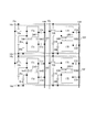
- FIG. 1 is an equivalent circuit diagram showing a part of the liquid crystal panel according to the first embodiment.
- the present liquid crystal panel includes a data signal line (15x ⁇ 15y) extending in the column direction (vertical direction in the drawing) and a scanning signal line (16x ⁇ 16y) extending in the row direction (horizontal direction in the drawing). ), Pixels (101 to 104) arranged in the row and column directions, storage capacitor lines (18p, 18q), and common electrode (counter electrode) com, and the structure of each pixel is the same.
- the pixel column including the pixels 101 and 102 and the pixel column including the pixels 103 and 104 are adjacent to each other, and the pixel row including the pixels 101 and 103 and the pixel row including the pixels 102 and 104 are adjacent to each other. is doing.
- one data signal line and one scanning signal line are provided corresponding to one pixel.
- Two pixel electrodes are arranged in the column direction in one pixel, and two pixel electrodes 17a and 17b provided in the pixel 101 and two pixel electrodes 17c and 17d provided in the pixel 102 are arranged in a line.
- two pixel electrodes 17A and 17B provided on the pixel 103 and two pixel electrodes 17C and 17D provided on the pixel 104 are arranged in a line, and the pixel electrodes 17a and 17A, the pixel electrodes 17b and 17B, Pixel electrodes 17c and 17C and pixel electrodes 17d and 17D are adjacent to each other in the row direction.
- the pixel electrodes 17a and 17b are connected via the coupling capacitors Cab1 and Cab2 arranged in parallel, and the pixel electrode 17a is connected to the data signal line 15x via the transistor 12a connected to the scanning signal line 16x.
- the storage capacitor Cha is formed between the pixel electrode 17a and the storage capacitor line 18p
- the storage capacitor Chb is formed between the pixel electrode 17b and the storage capacitor line 18p, and is connected between the pixel electrode 17a and the common electrode com.
- a liquid crystal capacitor Cla is formed, and a liquid crystal capacitor Clb is formed between the pixel electrode 17b and the common electrode com.
- the pixel electrodes 17c and 17d are connected via the coupling capacitors Ccd1 and Ccd2 arranged in parallel, and the pixel electrode 17c is connected to the scanning signal line 16y.
- a storage capacitor Chc is formed between the pixel electrode 17c and the storage capacitor line 18q
- a storage capacitor Chd is formed between the pixel electrode 17d and the storage capacitor line 18q.
- a liquid crystal capacitor Clc is formed between the pixel electrode 17c and the common electrode com
- a liquid crystal capacitor Cld is formed between the pixel electrode 17d and the common electrode com.
- the pixel electrodes 17A and 17B are connected via the coupling capacitors CAB1 and CAB2 arranged in parallel, and the pixel electrode 17A is connected to the scanning signal line 16x.
- a storage capacitor ChA is formed between the pixel electrode 17A and the storage capacitor line 18p
- a storage capacitor ChB is formed between the pixel electrode 17B and the storage capacitor line 18p.
- a liquid crystal capacitor ClA is formed between the pixel electrode 17A and the common electrode com
- a liquid crystal capacitor ClB is formed between the pixel electrode 17B and the common electrode com.
- the scanning signal lines 16x and 16y are sequentially selected.
- Vb Va ⁇ [(C1 + C2) / (Cl + Ch + C1 + C2)]]. That is,
- means a potential difference between Va and com potential Vcom), so that the subpixel including the pixel electrode 17a is a bright subpixel at the time of halftone display.
- the sub-pixel including the pixel electrode 17b is a dark sub-pixel, and display can be performed according to the area gradation of these bright / dark sub-pixels. Thereby, the viewing angle characteristic of the liquid crystal display device can be enhanced.
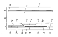
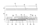
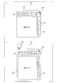
- FIG. 2 shows a specific example of the pixel 101 in FIG.
- a transistor 12a is arranged near the intersection of the data signal line 15x and the scanning signal line 16x, and a rectangular pixel electrode 17a is formed in a pixel region defined by both signal lines (15x and 16x).
- rectangular pixel electrodes 17b are arranged in the column direction, and one of the four sides forming the outer periphery of the first pixel electrode is adjacent to one of the four sides forming the outer periphery of the second pixel electrode.
- the first and second upper-layer capacitor electrodes 37a and 37b are arranged so as to overlap the gap between the two adjacent sides (the gap between the pixel electrodes 17a and 17b).
- the first lower layer capacitive electrode 47a is arranged so as to overlap the gap between the two adjacent sides (the gap between the pixel electrodes 17a and 17b) and the second upper layer capacitive electrode 37b (second conductor).
- the capacitor electrode 47b is disposed so as to overlap the gap between the two adjacent sides (the gap between the pixel electrodes 17a and 17b) and the first upper layer capacitor electrode 37a (first conductor).
- the storage capacitor line 18p includes a storage capacitor line extending portion branched from the storage capacitor line 18p, and is extended and overlapped with part of the edges of the pixel electrodes 17a and 17b in plan view.
- the first upper capacitor electrode 37a and the second upper capacitor electrode 37b are arranged side by side in the row direction, and the first lower capacitor electrode 47a and the second lower capacitor electrode are arranged.
- the capacitor electrode 47b is arranged in the row direction, the first upper layer capacitor electrode 37a and the second lower layer capacitor electrode 47b overlap, and the second upper layer capacitor electrode 37b and the first lower layer capacitor electrode 47a overlap.
- the parts are arranged side by side in the row direction.
- the storage capacitor wiring extending portion of the storage capacitor wiring 18p extends along the data signal lines 15x and 15y and the scanning signal lines 16x and 16y so as to surround the pixel region, and forms both sides of the pixel electrodes 17a and 17b.
- the storage capacitor wiring 18p It is extended and provided so as to overlap each of the three sides excluding. According to the shape of the storage capacitor wiring 18p, jumping in charges from the data signal lines 15x and 15y and the scanning signal lines 16x and 16y can be suppressed, so that an effect of improving the burn-in of the floating pixels can be obtained. Further, since the storage capacitor wiring 18p can be made redundant by the branching structure, the yield can be improved. Such a structure of the storage capacitor wiring 18p can be applied to each form of a liquid crystal panel described later, and the same effect can be obtained.
- the source electrode 8a and the drain electrode 9a of the transistor 12a are formed on the scanning signal line 16x, and the source electrode 8a is connected to the data signal line 15x.
- the drain electrode 9a is connected to the drain lead wiring 27a, and the drain lead wiring 27a is connected to the first upper layer capacitor electrode 37a formed in the same layer and is connected to the contact electrode 77a.
- the contact electrode 77a is connected via the contact hole 11a. To the pixel electrode 17a.
- the first upper capacitor electrode 37a overlaps with the second lower capacitor electrode 47b through the gate insulating film, and the second lower capacitor electrode extending portion 28b connected to the second lower capacitor electrode 47b is connected to the contact electrode 78b, and contact The electrode 78b is connected to the pixel electrode 17b through the contact hole 68b.
- a coupling capacitor Cab1 (see FIG. 1) between the pixel electrodes 17a and 17b is formed at an overlapping portion between the first upper layer capacitor electrode 37a and the second lower layer capacitor electrode 47b.
- the second upper layer capacitive electrode 37b overlaps the first lower layer capacitive electrode 47a via the gate insulating film, and the second upper layer capacitive electrode extending portion 29b connected to the second upper layer capacitive electrode 37b is connected to the contact electrode 79b.
- the contact electrode 79b is connected to the pixel electrode 17b through the contact hole 69b.
- the first lower capacitor electrode extension portion 29a connected to the first lower capacitor electrode 47a is connected to the contact electrode 79a, and the contact electrode 79a is connected to the pixel electrode 17a via the contact hole 69a.
- a coupling capacitor Cab2 (see FIG. 1) between the pixel electrodes 17a and 17b is formed at the overlapping portion between the second upper layer capacitor electrode 37b and the first lower layer capacitor electrode 47a.
- the pixel electrode 17a and the storage capacitor line 18p overlap with each other via the interlayer insulating film and the gate insulating film, and a storage capacitor Cha (see FIG. 1) is formed at the overlapping portion of both.
- the pixel electrode 17b and the storage capacitor line 18p overlap with each other via the interlayer insulating film and the gate insulating film, and a storage capacitor Chb (see FIG. 1) is formed at the overlapping portion between them. Note that the configuration of other pixels (the shape, arrangement, and connection relationship of each member) is the same as that of the pixel 101.
- the sub-pixel including the pixel electrode 17a is “bright”, and the sub-pixel including the pixel electrode 17b is “dark”.
- the coupling capacitors (Cab1 and Cab2) are formed by sandwiching the gate insulating film between the upper layer capacitor electrodes (37a and 37b) and the lower layer capacitor electrodes (47a and 47b). That is, in this configuration, the insulating film that forms the coupling capacitance is the gate insulating film.
- the insulating film that forms the coupling capacitance is an interlayer insulating film that covers the transistor. In general, since the gate insulating film is formed at a higher temperature than the interlayer insulating film covering the transistor, a denser film is more easily obtained with the gate insulating film.
- this configuration is preferable in that the occurrence of a short circuit between the electrodes in the coupling capacitance forming portion is suppressed as compared with the conventional configuration.
- Such a structure for forming a coupling capacitance by the gate insulating film can be applied to each mode of a liquid crystal panel described later, and the same effect can be obtained.
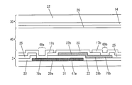
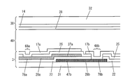
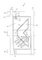
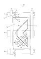
- FIG. 3 is a cross-sectional view taken along arrow X1-Y1 in FIG.
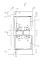
- the present liquid crystal panel includes an active matrix substrate 3, a color filter substrate 30 facing the active matrix substrate 3, and a liquid crystal layer 40 disposed between both substrates (3, 30).
- the second lower layer capacitor electrode 47b, the second lower layer capacitor electrode extending portion 28b, and the contact electrode 78b are formed on the glass substrate 31, and the inorganic gate insulating film 22 is formed so as to cover them.
- the scanning signal line is also formed on the substrate.
- the inorganic gate insulating film 22 are a semiconductor layer (i layer and n + layer; not shown), a source electrode and a drain electrode (both not shown) in contact with the n + layer, a drain lead wiring 27a, a first An upper capacitor electrode 37a and a contact electrode 77a are formed, and an inorganic interlayer insulating film 25 is formed so as to cover them.
- Pixel electrodes 17a and 17b are formed on the inorganic interlayer insulating film 25, and an alignment film (not shown) is formed so as to cover these (pixel electrodes 17a and 17b).
- the inorganic interlayer insulating film 25 is penetrated, whereby the pixel electrode 17a and the contact electrode 77a are connected.
- the inorganic interlayer insulating film 25 and the inorganic gate insulating film 22 are penetrated, whereby the pixel electrode 17b and the contact electrode 78b are connected. That is, the pixel electrode 17a and the first upper-layer capacitor electrode 37a are electrically connected, and the pixel electrode 17b and the second lower-layer capacitor electrode 47b are electrically connected. Then, the first upper capacitor electrode 37a and the second lower capacitor electrode 47b overlap with each other through the inorganic gate insulating film 22, thereby forming a coupling capacitor Cab1 (see FIG. 1).
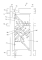
- FIG. 4 is a cross-sectional view taken along arrow X2-Y2 in FIG.
- a first lower layer capacitor electrode 47a, a first lower layer capacitor electrode extending portion 29a, and a contact electrode 79a are formed on the glass substrate 31 so as to cover them.
- An inorganic gate insulating film 22 is formed.
- the scanning signal line is also formed on the substrate.
- the inorganic gate insulating film 22 On top of the inorganic gate insulating film 22, there are a semiconductor layer (i layer and n + layer; not shown), a source electrode and a drain electrode (both not shown) in contact with the n + layer, a second upper capacitor electrode 37b, A second upper layer capacitor electrode extending portion 29b and a contact electrode 79b are formed, and an inorganic interlayer insulating film 25 is formed so as to cover them.
- Pixel electrodes 17a and 17b are formed on the inorganic interlayer insulating film 25, and an alignment film (not shown) is formed so as to cover these (pixel electrodes 17a and 17b).
- the inorganic interlayer insulating film 25 and the inorganic gate insulating film 22 are penetrated, whereby the pixel electrode 17a and the contact electrode 79a are connected.
- the inorganic interlayer insulating film 25 is penetrated so that the pixel electrode 17b and the contact electrode 79b are connected. That is, the pixel electrode 17a and the first lower layer capacitor electrode 47a are electrically connected, and the pixel electrode 17b and the second upper layer capacitor electrode 37b are electrically connected.
- the second upper capacitor electrode 37b and the first lower capacitor electrode 47a overlap with each other via the inorganic gate insulating film 22, thereby forming a coupling capacitor Cab2 (see FIG. 1).
- the colored layer 14 is formed on the glass substrate 32, and the common electrode (com) 28 is formed on the colored layer 14.
- a film (not shown) is formed.
- FIG. 5 is a timing chart showing a driving method of the present liquid crystal display device (normally black mode liquid crystal display device) provided with the liquid crystal panel shown in FIGS.
- Sv and SV indicate signal potentials supplied to two adjacent data signal lines (for example, 15x and 15y), and Gx and Gy are gate-on pulse signals supplied to the scanning signal lines 16x and 16y.
- Va ⁇ Vb, VA ⁇ VB, and Vc ⁇ Vd indicate the potentials of the pixel electrodes 17a and 17b, 17A and 17B, and 17c and 17d, respectively.
- the scanning signal lines are sequentially selected, the polarity of the signal potential supplied to the data signal lines is inverted every horizontal scanning period (1H), and the same number in each frame.
- the polarity of the signal potential supplied in the horizontal scanning period is inverted in units of one frame, and in the same horizontal scanning period, a signal potential having a reverse polarity is supplied to two adjacent data signal lines.
- the scanning signal lines are sequentially selected (for example, the scanning signal lines 16x and 16y are selected in this order), and one of the two adjacent data signal lines (for example, , A signal potential having a positive polarity is supplied to the data signal line 15x in the first horizontal scanning period (for example, including the writing period of the pixel electrode 17a), and the second horizontal scanning period (for example, writing of the pixel electrode 17c) is performed.
- a negative polarity signal potential is supplied to the other of the two data signal lines (for example, the data signal line 15y) for the first horizontal scanning period (for example, the writing period of the pixel electrode 17A).
- a subpixel including 17d is “dark”, a subpixel including pixel electrode 17A (minus polarity) is “bright”, and a subpixel including pixel electrode 17B (minus polarity) is “dark”. Is as shown in FIG.
- the scanning signal lines are sequentially selected (for example, the scanning signal lines 16x and 16y are selected in this order), and one of the two adjacent data signal lines (for example, the data signal line 15x) is the first.
- the negative polarity signal potential is supplied during the horizontal scanning period (for example, including the writing period of the pixel electrode 17a), and the positive polarity signal potential is supplied for the second horizontal scanning period (for example, including the writing period of the pixel electrode 17c).
- a positive polarity signal potential is supplied to the other of the two data signal lines (for example, the data signal line 15y) in the first horizontal scanning period (for example, including the writing period of the pixel electrode 17A).
- a negative polarity signal potential is supplied in the first horizontal scanning period (for example, including the writing period of the pixel electrode 17C). Accordingly, as shown in FIG. 5,
- , and the sub-pixel including the pixel electrode 17a (minus) is “bright”.
- the subpixel including the pixel electrode 17b (minus) is “dark”, the subpixel including the pixel electrode 17c (plus polarity) is “bright”, and the subpixel including the pixel electrode 17d (plus polarity) is “dark”.
- the sub-pixel including the electrode 17A (plus polarity) is “bright”, and the sub-pixel including the pixel electrode 17B (plus polarity) is “dark”, as shown in FIG. 6B as a whole.
- an alignment regulating slit is formed in the pixel electrode 17a.
- S1 to S4 are provided
- alignment regulating ribs L1 and L2 are provided in a portion corresponding to the pixel electrode 17a of the color filter substrate
- alignment regulating slits S5 to S8 are provided in the pixel electrode 17b, and the color filter substrate.
- Orientation regulating ribs L3 and L4 are provided at portions corresponding to the pixel electrodes 17b.
- an alignment regulating slit may be provided in the common electrode of the color filter substrate.
- the pixel electrode 17a and the pixel electrode 17b are connected (capacitively coupled) by two parallel coupling capacitors (Cab1 and Cab2).
- the capacitive coupling of the pixel electrodes 17a and 17b can be maintained by the second upper-layer capacitive electrode 37b even if the wire is disconnected (in the manufacturing process or the like).
- the drain lead-out wiring 27a is cut at a portion after the contact hole 11a, or the first upper layer capacitor electrode 47b is cut off.
- the electrode 37a is laser-cut at the connection point with the drain lead-out wiring 27a, or the second lower capacitor electrode 47b is laser-cut at the connection point with the pixel electrode 17b, thereby performing a correction process. 17b capacitive coupling can be maintained.
- the second upper layer capacitive electrode 37b and the first lower layer capacitive electrode 47a are short-circuited, the second upper layer capacitive electrode 37b is connected to the pixel electrode 17b or the first lower layer capacitive electrode 47a is connected to the pixel electrode 17a. Laser cutting may be performed at the connection point.
- the connection portion between the first upper layer capacitive electrode 37a and the pixel electrode 17a and the second lower layer capacitive electrode 47b and the pixel electrode 17b Laser cutting may be performed at both of the connection points.
- the connection point between the second upper layer capacitor electrode 37b and the pixel electrode 17b and the first lower layer capacitor electrode 47a and the pixel electrode 17a Laser cutting may be performed at both of the connection points.
- the drain lead-out wiring 27a (part after the contact hole 11a) is irradiated with a laser from the back surface (glass substrate side) of the active matrix substrate to cut it (see FIG. 7), or from the front surface of the active matrix substrate (opposite the glass substrate), the first upper-layer capacitor electrode 37a is irradiated with laser through the gap between the pixel electrodes 17a and 17b to cut it. Will do.
- the method of irradiating the laser from the front surface of the active matrix substrate to cut the first upper-layer capacitor electrode 37a has an advantage that the active matrix substrate does not need to be inverted during the correction process.
- the drain lead-out wiring 27a (part after the contact hole 11a) is irradiated with laser from the back surface of the liquid crystal panel (the glass substrate side of the active matrix substrate) to cut it
- the first upper capacitor electrode 37a may be irradiated with a laser through the gap between the pixel electrodes 17a and 17b to cut it.
- the present embodiment it is possible to increase the manufacturing yield of the liquid crystal panel and the active matrix substrate used therefor.
- the conventional active matrix substrate (reference) shown in FIG. 48 if the lead wiring 119 is disconnected, the potential control of the pixel electrode 121b becomes impossible.
- the control electrode 118 and the capacitor wiring 113 are short-circuited, the signal potential can be written to the pixel electrode 121a by cutting the lead-out wiring 119, but the pixel electrode 121b is connected to the pixel electrode 121a. Capacitive coupling is lost.
- the first and second lower capacitive electrodes 47a and 47b have a larger area than the first and second upper capacitive electrodes 37a and 37b. Even in this case, the overlapping area of the first lower capacitor electrode 47a and the second upper capacitor electrode 37b and the overlapping area of the second lower capacitor electrode 47b and the first upper capacitor electrode 37a, that is, the total amount of the two coupling capacitors (Cab1 ⁇ Cab2). There is an advantage that is difficult to change.
- Each of the first and second upper capacitive electrodes 37a and 37b may have a larger area than the first and second lower capacitive electrodes 47a and 47b. In this case, the same effect as described above can be obtained.
- the method for manufacturing a liquid crystal panel includes an active matrix substrate manufacturing process, a color filter substrate manufacturing process, and an assembly process in which both substrates are bonded to each other and filled with liquid crystal. Further, an inspection process is performed during or after at least one of the active matrix substrate manufacturing process and the assembly process, and when a pixel (sub-pixel) defect is detected in the inspection process, a correction process for correcting the defect is added.
- a metal film such as titanium, chromium, aluminum, molybdenum, tantalum, tungsten, or copper, an alloy film thereof, or a laminated film thereof (thickness: 1000 mm to 3000 mm) is sputtered onto a substrate such as glass or plastic. Then, patterning is performed by photolithography technology (Photo Engraving Process, hereinafter referred to as “PEP technology”), and scanning signal lines and transistor gate electrodes (the scanning signal lines may also serve as gate electrodes) Then, a gate metal layer (first and second lower layer capacitor electrodes 47a and 47b) and a storage capacitor line are formed.
- PEP technology Photo Engraving Process
- an inorganic insulating film such as silicon nitride or silicon oxide is formed by CVD (Chemical Vapor Deposition) method on the entire substrate on which the scanning signal lines are formed, thereby forming a gate insulating film To do.
- CVD Chemical Vapor Deposition
- silicon nitride is formed at a substrate temperature of 350 ° C. during film formation.
- an intrinsic amorphous silicon film (thickness 1000 to 3000 mm) and an n + amorphous silicon film (thickness 400 to 700 mm) doped with phosphorus are continuously formed on the gate insulating film (whole substrate) by CVD.
- patterning is performed by the PEP technique, and a silicon laminated body including an intrinsic amorphous silicon layer and an n + amorphous silicon layer is formed in an island shape on the gate electrode.
- a metal film such as titanium, chromium, aluminum, molybdenum, tantalum, tungsten, or copper, an alloy film thereof, or a stacked film thereof (thickness 1000 to 3000 mm) is formed on the entire substrate on which the silicon laminate is formed. Then, patterning is performed by the PEP technique, and data signal lines, transistor source / drain electrodes, drain lead wires, and conductors (first and second upper-layer capacitor electrodes 37a and 37b) are formed. Form.
- the n + amorphous silicon layer constituting the silicon stacked body is removed by etching to form a transistor channel.
- the semiconductor layer may be formed of an amorphous silicon film as described above.
- a polysilicon film may be formed, or a laser annealing treatment is performed on the amorphous silicon film and the polysilicon film to form a crystal. May be improved. Thereby, the moving speed of the electrons in the semiconductor layer is increased, and the characteristics of the transistor (TFT) can be improved.
- an inorganic insulating film such as silicon nitride or silicon oxide is formed by CVD on the entire substrate on which the data signal lines and the like are formed to form an inorganic interlayer insulating film.
- silicon nitride is formed at a substrate temperature of 250 ° C. during film formation.
- the interlayer insulating film, or the interlayer insulating film and the gate insulating film are removed by etching using PEP technology to form various contact holes.
- a transparent conductive film (thickness 1000 to 2000 mm) made of ITO (Indium / Tin / Oxide), IZO (Indium / Zinc / Oxide), zinc oxide, tin oxide or the like is formed on the entire substrate on the interlayer insulating film in which the contact holes are formed. Is formed by sputtering, and then patterned by PEP technology to form each pixel electrode.
- polyimide resin is printed on the entire substrate on the pixel electrode with a thickness of 500 to 1000 mm, and then fired and rubbed in one direction with a rotating cloth to form an alignment film.
- the active matrix substrate is manufactured as described above.
- the color filter substrate manufacturing process will be described below.
- a chromium thin film or a resin containing a black pigment is formed on a glass or plastic substrate (entire substrate), and then patterned by PEP technology to form a black matrix.
- red, green and blue color filter layers are formed in a pattern in the gap of the black matrix by using a pigment dispersion method or the like.
- a transparent conductive film made of ITO, IZO, zinc oxide, tin oxide or the like is formed on the entire substrate on the color filter layer to form a common electrode (com).
- polyimide resin is printed on the entire substrate on the common electrode with a thickness of 500 to 1000 mm, and then fired and rubbed in one direction with a rotating cloth to form an alignment film.
- a color filter substrate can be manufactured as described above.
- a seal material made of a thermosetting epoxy resin or the like is applied to one of the active matrix substrate and the color filter substrate by screen printing in a frame-like pattern lacking the liquid crystal inlet portion, and the liquid crystal layer is applied to the other substrate.
- a spherical spacer having a diameter corresponding to the thickness and made of plastic or silica is dispersed.
- the active matrix substrate and the color filter substrate are bonded together, and the sealing material is cured.
- the liquid crystal panel is manufactured.
- a short-circuit occurrence location is detected by performing an appearance inspection or an electro-optical inspection on the active matrix substrate.
- the short circuit for example, a short circuit between the conductor (first and second upper-layer capacitor electrodes 37a and 37b) and the capacitor electrode (first and second lower-layer capacitor electrodes 47a and 47b), or the conductor (first and second capacitor electrodes).
- the appearance inspection is to optically inspect the wiring pattern using a CCD camera or the like.
- the electro-optical inspection is an active inspection after a modulator (electro-optical element) is placed so as to face the active matrix substrate.
- a wiring pattern is electro-optically inspected by applying a voltage between a matrix substrate and a modulator and making light incident and capturing a change in luminance of the light with a CCD camera.
- a correction process is performed in which the short-circuited conductor or a conductor portion connected to the short-circuited conductor (for example, a drain lead wiring) is laser-cut.
- a fourth harmonic (wavelength 266 nm) of a YAG (Yttrium Aluminum Garnet) laser is used.
- a correction process may be performed in which a portion in the contact hole is removed (trimmed) by a laser or the like among pixel electrodes connected to the short-circuited conductor via the contact hole. .
- laser irradiation can usually be performed from the front surface (pixel electrode side) or the back surface (substrate side) of the active matrix substrate.
- the first inspection process and the correction process may be performed after the formation of the conductors (first and second upper-layer capacitor electrodes 37a and 37b) or after the formation of the channel of the transistor in addition to the formation of the pixel electrode. In this way, defects can be corrected at an earlier stage of the manufacturing process, and the manufacturing yield of the active matrix substrate can be increased.
- a short circuit location is detected by performing a lighting inspection on the liquid crystal panel.
- a short circuit for example, a short circuit between the first and second upper capacitive electrodes 37a and 37b and the capacitive electrodes (first and second lower capacitive electrodes 47a and 47b), and the first and second upper capacitive electrodes 37a and 37b.
- the data signal lines 15x and 15y There is a short circuit with the data signal lines 15x and 15y.
- a gate inspection signal having a bias voltage of ⁇ 10 V, a period of 16.7 msec, a pulse width of 50 ⁇ sec and a pulse voltage of +15 V is input to each scanning signal line to turn on all TFTs.
- a source inspection signal having a potential of ⁇ 2 V whose polarity is inverted every 16.7 msec is input to each data signal line, and a signal potential corresponding to ⁇ 2 V is applied to the pixel electrode via the source electrode and the drain electrode of each TFT.
- a common electrode inspection signal having a direct current potential of ⁇ 1 V is input to the common electrode (com) and the storage capacitor wiring.
- a voltage is applied to the liquid crystal capacitor formed between the pixel electrode and the common electrode, and the storage capacitor formed between the storage capacitor wiring and the pixel electrode, and the sub-pixel formed by the pixel electrode is turned on. It becomes a state. For example, at a short-circuited portion between the conductor and the data signal line, the pixel electrode and the data signal line are electrically connected to become a bright spot (normally black). Thereby, a short circuit location is detected.
- a correction process is performed in which the short-circuited conductor or a conductor portion connected to the short-circuited conductor (for example, a drain lead wiring) is laser-cut.
- laser irradiation is usually performed from the back surface of the active matrix substrate (the substrate side of the active matrix substrate).
- an organic interlayer insulating film thicker than this is provided on the inorganic interlayer insulating film 25 of FIG. 3, and the channel protective film (interlayer insulating film) has a two-layer structure as shown in FIG. it can. In this way, effects such as reduction of various parasitic capacitances, prevention of short-circuiting between wirings, and reduction of pixel electrode tearing due to planarization can be obtained.
- the inorganic interlayer insulating film 25, the organic interlayer insulating film 26, and the contact holes 11a and 68b in FIG. 8 can be formed as follows, for example. That is, after forming the transistors and data signal lines, an inorganic interlayer insulating film 25 made of SiNx having a thickness of about 3000 mm so as to cover the entire surface of the substrate using a mixed gas of SiH 4 gas, NH 3 gas, and N 2 gas. (Passivation film) is formed by CVD. Thereafter, an organic interlayer insulating film 26 made of a positive photosensitive acrylic resin having a thickness of about 3 ⁇ m is formed by spin coating or die coating.
- CF 4 gas and O 2 gas are mixed.
- the inorganic interlayer insulating film 25 is dry-etched at the contact hole 11a, and the inorganic interlayer insulating film 25 and the gate insulating film 22 are dry-etched at the contact hole 68b.
- the organic insulating film is half-exposed in the photolithography process so that the organic interlayer insulating film remains thin when development is completed, while the contact hole 68b The portion is fully exposed in the photolithography process so that no organic interlayer insulating film remains when development is completed.
- dry etching is performed with a mixed gas of CF 4 gas and O 2 gas, the remaining film (of the organic interlayer insulating film) is first removed from the contact hole 11a, and then the inorganic interlayer insulating film 25 is removed.
- the inorganic interlayer insulating film 25 under the organic interlayer insulating film is removed first, and then the gate insulating film 22 is removed.
- the organic interlayer insulating film 26 may be, for example, an insulating film made of an SOG (spin-on glass) material, and the organic interlayer insulating film 26 may be an acrylic resin, an epoxy resin, a polyimide resin, a polyurethane resin, or a novolac resin. , And at least one of siloxane resins may be included.
- SOG spin-on glass
- the drain electrode 9a of the transistor 12a is connected to the pixel electrode 17a through the contact hole 11a, and the pixel electrode 17a and the first upper-layer capacitor electrode 37a are connected through the contact hole 68a.
- the drain lead wiring connecting the drain electrode 9a and the first upper-layer capacitor electrode 37a can be shortened, and the aperture ratio can be increased.
- the pixel electrode 17a and the pixel electrode 17b are connected (capacitively coupled) by two coupling capacitors (Cab1 and Cab2) in parallel, a contact hole 68a is formed in the manufacturing process or the like.
- Capacitive coupling between the pixel electrodes 17a and 17b can be maintained by removing (trimming) the portion in the contact hole 68a with a laser or the like and electrically separating the pixel electrode 17a and the first upper-layer capacitor electrode 37a.
- one of the two pixel electrodes provided in one pixel that is closer to the transistor is connected to the transistor.
- the present invention is not limited to this. As shown in FIG. 11, the farther from the transistor of the two pixel electrodes provided in one pixel may be connected to the transistor.
- FIG. 12 shows a specific example of the pixel 101 in FIG.
- a transistor 12a is disposed in the vicinity of the intersection of the data signal line 15x and the scanning signal line 16x, and a rectangular pixel electrode 17a is formed in a pixel region defined by both signal lines (15x and 16x).
- Rectangular pixel electrodes 17b are arranged in the column direction, and one of the four sides forming the outer periphery of the first pixel electrode is adjacent to one of the four sides forming the outer periphery of the second pixel electrode. Yes.
- the first and second upper-layer capacitor electrodes 37a and 37b are arranged so as to overlap the gap between the adjacent two sides (the gap between the pixel electrodes 17a and 17b), the pixel electrode 17a, and the pixel electrode 17b.
- the first lower layer capacitor electrode 47a is arranged so as to overlap the gap between the two adjacent sides (the gap between the pixel electrodes 17a and 17b) and the second upper layer capacitor electrode 37b. They are arranged so as to overlap the gap between two adjacent sides (the gap between the pixel electrodes 17a and 17b) and the first upper-layer capacitor electrode 37a.
- the storage capacitor line 18p includes a storage capacitor line extending portion branched from the storage capacitor line 18p, and is extended and overlapped with part of the edges of the pixel electrodes 17a and 17b in plan view.
- the first upper capacitor electrode 37a and the second upper capacitor electrode 37b are arranged side by side in the row direction, and the first lower capacitor electrode 47a and the second lower capacitor electrode are arranged.
- the capacitor electrode 47b is arranged in the row direction, the first upper layer capacitor electrode 37a and the second lower layer capacitor electrode 47b overlap, and the second upper layer capacitor electrode 37b and the first lower layer capacitor electrode 47a overlap.
- the parts are arranged side by side in the row direction.
- the storage capacitor line extending portion of the storage capacitor line 18p is provided so as to surround the pixel region, and overlaps three sides excluding both sides forming the gap between the pixel electrodes 17a and 17b.
- the source electrode 8a and the drain electrode 9a of the transistor 12a are formed on the scanning signal line 16x, and the source electrode 8a is connected to the data signal line 15x.
- the drain electrode 9a is connected to the drain lead wiring 27a, and the drain lead wiring 27a is connected to the second upper layer capacitor electrode 37b formed in the same layer.
- the second upper layer capacitor electrode extending portion 29b connected to the second upper layer capacitor electrode 37b is connected to the contact electrode 79b, and the contact electrode 79b is connected to the pixel electrode 17b through the contact hole 69b.
- the second upper layer capacitor electrode 37b overlaps the first lower layer capacitor electrode 47a through the gate insulating film, and the first lower layer capacitor electrode extending portion 29a connected to the first lower layer capacitor electrode 47a is connected to the contact electrode 79a to be contacted.
- the electrode 79a is connected to the pixel electrode 17a through the contact hole 69a.
- a coupling capacitance Cab2 (see FIG. 11) between the pixel electrodes 17a and 17b is formed at an overlapping portion between the second upper layer capacitor electrode 37b and the first lower layer capacitor electrode 47a.
- the first upper capacitor electrode 37a overlaps the second lower capacitor electrode 47b through the gate insulating film, and the first upper capacitor electrode extending portion 28a connected to the first upper capacitor electrode 37a is connected to the contact electrode 78a.
- the contact electrode 78a is connected to the pixel electrode 17a through the contact hole 68a.
- the second lower layer capacitor electrode extending portion 28b connected to the second lower layer capacitor electrode 47b is connected to the contact electrode 78b, and the contact electrode 78b is connected to the pixel electrode 17b through the contact hole 68b.
- a coupling capacitor Cab1 (see FIG. 11) between the pixel electrodes 17a and 17b is formed at the overlapping portion between the first upper layer capacitor electrode 37a and the second lower layer capacitor electrode 47b.
- the pixel electrode 17a and the storage capacitor line 18p overlap with each other via the interlayer insulating film and the gate insulating film, and a storage capacitor Cha (see FIG. 11) is formed at the overlapping portion between them.
- the pixel electrode 17b and the storage capacitor line 18p overlap with each other via the interlayer insulating film and the gate insulating film, and a storage capacitor Chb (see FIG. 11) is formed in the overlapping portion between them.
- the configuration of other pixels (the shape, arrangement, and connection relationship of each member) is the same as that of the pixel 101.
- the sub-pixel including the pixel electrode 17a is “dark”, and the sub-pixel including the pixel electrode 17b is “bright”.
- the second upper layer at P in FIG. 12 since the pixel electrode 17a and the pixel electrode 17b are connected (capacitively coupled) by two parallel coupling capacitors (Cab1 and Cab2), for example, the second upper layer at P in FIG.
- the capacitor electrode 37b and the first lower layer capacitor electrode 47a are short-circuited (in a manufacturing process or the like), the second upper layer capacitor electrode 37b is laser-cut between the connection point with the pixel electrode 17b and the short-circuit point.
- the capacitive coupling of the pixel electrodes 17a and 17b can be maintained.
- the first upper-layer capacitor electrode 37a and the second lower-layer capacitor electrode 47b are short-circuited, the first upper-layer capacitor electrode 37a may be laser-cut between the connection point with the pixel electrode 17a and the short-circuit point. Good.
- the first and second lower layer capacitive electrodes 47a and 47b have a larger area than the first and second upper layer capacitive electrodes 37a and 37b, so that the alignment of each capacitive electrode is shifted to some extent. Even in this case, the overlapping area of the first lower capacitive electrode 47a and the second upper capacitive electrode 37b and the overlapping area of the second lower capacitive electrode 47b and the first upper capacitive electrode 37a, that is, the total amount of the coupling capacitances (Cab1 and Cab2) are changed. There is a merit that it is difficult to do.
- Each of the first and second upper capacitive electrodes 37a and 37b may have a larger area than the first and second lower capacitive electrodes 47a and 47b. In this case, the same effect as described above can be obtained.
- the pixel electrode closer to the transistor is connected to the transistor, but the present invention is not limited to this. As shown in FIG. 13, the pixel electrode closer to the transistor is connected to the transistor on one of the two pixels adjacent in the row direction, and the pixel electrode farther from the transistor is connected to the transistor on the other side. Good.
- the sub-pixel including the pixel electrode 17a (positive polarity) is “bright”, and the pixel electrode 17b
- the subpixel including (positive polarity) is “dark”
- the subpixel including the pixel electrode 17c (minus polarity) is “bright”
- the subpixel including the pixel electrode 17d (minus polarity) is “dark”
- the pixel electrode 17A The sub-pixel including (minus polarity) is “dark”
- the sub-pixel including the pixel electrode 17B (minus polarity) is “bright”, as a whole, as shown in FIG.
- the subpixel including the pixel electrode 17a is “bright”
- the subpixel including the pixel electrode 17b is “minus polarity”
- the subpixel including the pixel electrode 17c is “plus polarity”.
- the subpixel including the pixel electrode 17d positive polarity
- the subpixel including the pixel electrode 17A positive polarity
- the subpixel including the pixel electrode 17B positive polarity
- FIG. 15 shows a specific example of the pixels 101 and 103 in FIG.
- a transistor 12a is disposed in the vicinity of the intersection of the data signal line 15x and the scanning signal line 16x, and the pixel region defined by both signal lines (15x and 16x) has a rectangular shape.
- the pixel electrode 17a and the rectangular pixel electrode 17b are arranged in the column direction, and one of the four sides forming the outer periphery of the first pixel electrode and one of the four sides forming the outer periphery of the second pixel electrode. And are adjacent.
- the first and second upper-layer capacitor electrodes 37a and 37b are arranged so as to overlap the gap between the two adjacent sides (the gap between the pixel electrodes 17a and 17b).
- the first lower layer capacitor electrode 47a is arranged so as to overlap the gap between the two adjacent sides (the gap between the pixel electrodes 17a and 17b) and the second upper layer capacitor electrode 37b. They are arranged so as to overlap the gap between two adjacent sides (the gap between the pixel electrodes 17a and 17b) and the first upper-layer capacitor electrode 37a.
- the storage capacitor line 18p includes a storage capacitor line extending portion branched from the storage capacitor line 18p, and is extended and overlapped with part of the edges of the pixel electrodes 17a and 17b in plan view.
- the first upper capacitor electrode 37a and the second upper capacitor electrode 37b are arranged side by side in the row direction, and the first lower capacitor electrode 47a and the second lower capacitor electrode are arranged.
- the capacitor electrode 47b is arranged in the row direction, the first upper layer capacitor electrode 37a and the second lower layer capacitor electrode 47b overlap, and the second upper layer capacitor electrode 37b and the first lower layer capacitor electrode 47a overlap.
- the parts are arranged side by side in the row direction.
- the storage capacitor line extending portion of the storage capacitor line 18p is provided so as to surround the pixel region, and overlaps three sides excluding both sides forming the gap between the pixel electrodes 17a and 17b.
- the source electrode 8a and the drain electrode 9a of the transistor 12a are formed on the scanning signal line 16x, and the source electrode 8a is connected to the data signal line 15x.
- the drain electrode 9a is connected to the drain lead wiring 27a, and the drain lead wiring 27a is connected to the first upper layer capacitor electrode 37a formed in the same layer and is connected to the contact electrode 77a.
- the contact electrode 77a is connected via the contact hole 11a. To the pixel electrode 17a.
- the first upper capacitor electrode 37a overlaps with the second lower capacitor electrode 47b through the gate insulating film, and the second lower capacitor electrode extending portion 28b connected to the second lower capacitor electrode 47b is connected to the contact electrode 78b, and contact The electrode 78b is connected to the pixel electrode 17b through the contact hole 68b.
- a coupling capacitor Cab1 (see FIG. 13) between the pixel electrodes 17a and 17b is formed at the overlapping portion between the first upper layer capacitor electrode 37a and the second lower layer capacitor electrode 47b.
- the second upper layer capacitive electrode 37b overlaps the first lower layer capacitive electrode 47a via the gate insulating film, and the second upper layer capacitive electrode extending portion 29b connected to the second upper layer capacitive electrode 37b is connected to the contact electrode 79b.
- the contact electrode 79b is connected to the pixel electrode 17b through the contact hole 69b.
- the first lower capacitor electrode extension portion 29a connected to the first lower capacitor electrode 47a is connected to the contact electrode 79a, and the contact electrode 79a is connected to the pixel electrode 17a via the contact hole 69a.
- a coupling capacitor Cab2 (see FIG. 13) between the pixel electrodes 17a and 17b is formed at the overlapping portion between the second upper layer capacitor electrode 37b and the first lower layer capacitor electrode 47a.
- the pixel electrode 17a and the storage capacitor line 18p are overlapped with each other through the interlayer insulating film and the gate insulating film, and a storage capacitor Cha (see FIG. 13) is formed at the overlapping portion between them. Further, the pixel electrode 17b and the storage capacitor line 18p are overlapped with each other via the interlayer insulating film and the gate insulating film, and a storage capacitor Chb (see FIG. 13) is formed in the overlapping portion between them.
- the sub-pixel including the pixel electrode 17a is “bright”, and the sub-pixel including the pixel electrode 17b is “dark”.
- a transistor 12A is disposed in the vicinity of the intersection of the data signal line 15y and the scanning signal line 16x, and a rectangular pixel electrode 17A and a rectangular shape are formed in a pixel region defined by both signal lines (15y ⁇ 16x).
- the pixel electrodes 17B having a shape are arranged in the column direction, and one of the four sides forming the outer periphery of the first pixel electrode is adjacent to one of the four sides forming the outer periphery of the second pixel electrode. .
- the first and second upper-layer capacitor electrodes 37A and 37B are arranged so as to overlap the gap between the two adjacent sides (the gap between the pixel electrodes 17A and 17B).
- the first lower-layer capacitor electrode 47A is arranged so as to overlap the gap between the two adjacent sides (the gap between the pixel electrodes 17A and 17B) and the second upper-layer capacitor electrode 37B. They are arranged so as to overlap the gap between two adjacent sides (the gap between the pixel electrodes 17A and 17B) and the first upper-layer capacitor electrode 37A.
- the storage capacitor line 18p includes a storage capacitor line extending portion branched from the storage capacitor line 18p, and is provided to extend so as to overlap part of the edges of the pixel electrodes 17A and 17B in a plan view.
- the first upper capacitor electrode 37A and the second upper capacitor electrode 37B are arranged side by side in the row direction, and the first lower capacitor electrode 47A and the second lower capacitor electrode are arranged.
- the capacitive electrode 47B is arranged in the row direction, the first upper capacitive electrode 37A and the second lower capacitive electrode 47B overlap, and the second upper capacitive electrode 37B and the first lower capacitive electrode 47A overlap.
- the parts are arranged side by side in the row direction.
- the storage capacitor line extending portion of the storage capacitor line 18p is provided so as to surround the pixel region, and overlaps each of the three sides excluding both sides forming the gap between the pixel electrodes 17A and 17B.
- the source electrode 8A and the drain electrode 9A of the transistor 12A are formed on the scanning signal line 16x, and the source electrode 8A is connected to the data signal line 15y.
- the drain electrode 9A is connected to the drain lead wiring 27A, and the drain lead wiring 27A is connected to the second upper layer capacitor electrode 37B formed in the same layer.
- the second upper layer capacitor electrode extending portion 29B connected to the second upper layer capacitor electrode 37B is connected to the contact electrode 79B, and the contact electrode 79B is connected to the pixel electrode 17B through the contact hole 69B.
- the second upper layer capacitive electrode 37B overlaps the first lower layer capacitive electrode 47A via the gate insulating film, and the first lower layer capacitive electrode extending portion 29A connected to the first lower layer capacitive electrode 47A is connected to the contact electrode 79A for contact.
- the electrode 79A is connected to the pixel electrode 17A through the contact hole 69A.
- a coupling capacitor CAB2 (see FIG. 13) between the pixel electrodes 17A and 17B is formed at the overlapping portion of the second upper layer capacitor electrode 37B and the first lower layer capacitor electrode 47A.
- the first upper capacitor electrode 37A overlaps with the second lower capacitor electrode 47B through the gate insulating film, and the first upper capacitor electrode extension portion 28A connected to the first upper capacitor electrode 37A is connected to the contact electrode 78A.
- the contact electrode 78A is connected to the pixel electrode 17A through the contact hole 68A.
- the second lower layer capacitor electrode extending portion 28B connected to the second lower layer capacitor electrode 47B is connected to the contact electrode 78B, and the contact electrode 78B is connected to the pixel electrode 17B through the contact hole 68B.
- a coupling capacitor CAB1 (see FIG. 13) between the pixel electrodes 17A and 17B is formed at the overlapping portion between the first upper layer capacitor electrode 37A and the second lower layer capacitor electrode 47B.
- the pixel electrode 17A and the storage capacitor line 18p are overlapped with each other via the interlayer insulating film and the gate insulating film, and a storage capacitor ChA (see FIG. 13) is formed at the overlapping portion between them. Further, the pixel electrode 17B and the storage capacitor line 18p overlap with each other via the interlayer insulating film and the gate insulating film, and a storage capacitor ChB (see FIG. 13) is formed in the overlapping portion between them.
- the sub-pixel including the pixel electrode 17A is “dark”, and the sub-pixel including the pixel electrode 17B is “bright”.
- FIG. 2 and FIG. 9 may be modified as shown in FIG.
- the first lower layer capacitive electrode 47a in FIG. 9 is omitted, and in the region overlapping the pixel electrode 17a, the first upper layer capacitive electrode 37a and the second upper layer capacitive electrode 37b are arranged side by side in the row direction.
- the first upper capacitor electrode 37a and the second lower capacitor electrode 47b overlap.
- the storage capacitor line extending portion of the storage capacitor line 18p is provided so as to surround the pixel region, and overlaps three sides excluding both sides forming the gap between the pixel electrodes 17a and 17b.
- the source electrode 8a and the drain electrode 9a of the transistor 12a are formed on the scanning signal line 16x, and the source electrode 8a is connected to the data signal line 15x.
- the drain electrode 9a is connected to the drain lead wiring 27a, the drain lead wiring 27a is connected to the contact electrode 77a, and the contact electrode 77a is connected to the pixel electrode 17a through the contact hole 11a.
- the first upper layer capacitive electrode 37a overlaps the second lower layer capacitive electrode 47b through the gate insulating film, and the first upper layer capacitive electrode extending portion 28a connected to the first upper layer capacitive electrode 37a is connected to the contact electrode 78a.
- the electrode 78a is connected to the pixel electrode 17a through the contact hole 68a.
- the second lower layer capacitor electrode extending portion 28b connected to the second lower layer capacitor electrode 47b is connected to the contact electrode 78b, and the contact electrode 78b is connected to the pixel electrode 17b through the contact hole 68b.
- a coupling capacitor Cab1 (see FIG. 1) between the pixel electrodes 17a and 17b is formed at an overlapping portion between the first upper layer capacitor electrode 37a and the second lower layer capacitor electrode 47b.
- the second upper-layer capacitor electrode 37b overlaps the pixel electrode 17a via an interlayer insulating film.
- the second upper layer capacitor electrode extending portion 29b connected to the second upper layer capacitor electrode 37b is connected to the contact electrode 79b, and the contact electrode 79b is connected to the pixel electrode 17b via the contact hole 69b.
- a coupling capacitor Cab2 (see FIG. 1) between the pixel electrodes 17a and 17b is formed at the overlapping portion between the second upper layer capacitive electrode 37b and the pixel electrode 17a.
- the pixel electrode 17a and the storage capacitor line 18p overlap with each other via the interlayer insulating film and the gate insulating film, and a storage capacitor Cha (see FIG. 1) is formed at the overlapping portion of both.
- the pixel electrode 17b and the storage capacitor line 18p overlap with each other via the interlayer insulating film and the gate insulating film, and a storage capacitor Chb (see FIG. 1) is formed at the overlapping portion between them. Note that the configuration of other pixels (the shape, arrangement, and connection relationship of each member) is the same as that of the pixel 101.
- the sub-pixel including the pixel electrode 17a is “bright”, and the sub-pixel including the pixel electrode 17b is “dark”.
- FIG. 17 is a cross-sectional view taken along arrow X1-Y1 in FIG.
- the present liquid crystal panel includes an active matrix substrate 3, a color filter substrate 30 facing the active matrix substrate 3, and a liquid crystal layer 40 disposed between both substrates (3, 30).
- the second lower layer capacitor electrode 47b, the second lower layer capacitor electrode extending portion 28b, and the contact electrode 78b are formed on the glass substrate 31, and the inorganic gate insulating film 22 is formed so as to cover them.
- the scanning signal line is also formed on the substrate.
- a semiconductor layer (i layer and n + layer; not shown), a source electrode and a drain electrode (both not shown) in contact with the n + layer, a first upper capacitor electrode 37a, A first upper-layer capacitor electrode extending portion 28a and a contact electrode 78a are formed, and an inorganic interlayer insulating film 25 is formed so as to cover them.
- Pixel electrodes 17a and 17b are formed on the inorganic interlayer insulating film 25, and an alignment film (not shown) is formed so as to cover these (pixel electrodes 17a and 17b).
- the inorganic interlayer insulating film 25 is penetrated, whereby the pixel electrode 17a and the contact electrode 78a are connected.
- the inorganic interlayer insulating film 25 and the inorganic gate insulating film 22 are penetrated, whereby the pixel electrode 17b and the contact electrode 78b are connected. That is, the pixel electrode 17a and the first upper-layer capacitor electrode 37a are electrically connected, and the pixel electrode 17b and the second lower-layer capacitor electrode 47b are electrically connected. Then, the first upper capacitor electrode 37a and the second lower capacitor electrode 47b overlap with each other through the inorganic gate insulating film 22, thereby forming a coupling capacitor Cab1 (see FIG. 1).
- a pixel electrode 17a is formed on the first upper capacitive electrode 37a with the inorganic interlayer insulating film 25 interposed therebetween.
- an inorganic gate insulating film 22 is formed on a glass substrate 31.
- the scanning signal line is also formed on the substrate.
- Pixel electrodes 17a and 17b are formed on the inorganic interlayer insulating film 25, and an alignment film (not shown) is formed so as to cover these (pixel electrodes 17a and 17b).
- the inorganic interlayer insulating film 25 is penetrated in the contact hole 69b, whereby the pixel electrode 17b and the contact electrode 79b are connected. That is, the pixel electrode 17b and the second upper layer capacitor electrode 37b are electrically connected. Then, the second upper layer capacitor electrode 37b and the pixel electrode 17a overlap with each other via the inorganic interlayer insulating film 25, thereby forming a coupling capacitor Cab2 (see FIG. 1).
- the colored layer 14 is formed on the glass substrate 32, the common electrode (com) 28 is formed on the upper layer, and the orientation is further covered.
- a film (not shown) is formed.
- the pixel electrode 17a and the pixel electrode 17b are connected (capacitively coupled) by two coupling capacitors ((Cab1) and (Cab2)) arranged in parallel in a plane.
- the first upper-layer capacitor electrode 37a and the second lower-layer capacitor electrode 47b or the data signal line 15x are short-circuited (in the manufacturing process or the like) at P, the first upper-layer capacitor electrode 37a is connected to the contact hole 68a.
- the capacitive coupling of the pixel electrodes 17a and 17b can be maintained.
- the pixel electrode 17b and the first upper-layer capacitor electrode 37a are conductive and have the same potential. Capacitive coupling between the pixel electrode 17a and the pixel electrode 17b can be maintained by overlapping the first upper layer capacitive electrode 37a and the pixel electrode 17a with the inorganic interlayer insulating film 25 interposed therebetween.
- the 16 may be modified as shown in FIG. In the configuration of FIG. 19, in the region overlapping the pixel electrode 17b, the first upper-layer capacitor electrode 37a and the second upper-layer capacitor electrode 37b are arranged side by side in the row direction, and the second upper-layer capacitor electrode 37b and the first lower-layer capacitor electrode 47a. And overlap.
- the first upper-layer capacitor electrode 37a overlaps the pixel electrode 17b via the interlayer insulating film, and the first upper-layer capacitor electrode extending portion 28a connected to the first upper-layer capacitor electrode 37a is connected to the contact electrode 78a.
- the contact electrode 78a is connected to the pixel electrode 17a through the contact hole 68a.
- a coupling capacitance Cab1 (see FIG. 1) between the pixel electrodes 17a and 17b is formed at the overlapping portion between the first upper layer capacitive electrode 37a and the pixel electrode 17b.
- the second upper layer capacitive electrode 37b overlaps the first lower layer capacitive electrode 47a via the gate insulating film, and the second upper layer capacitive electrode extending portion 29b connected to the second upper layer capacitive electrode 37b is connected to the contact electrode 79b.
- the contact electrode 79b is connected to the pixel electrode 17b through the contact hole 69b.
- the first lower capacitor electrode extension portion 29a connected to the first lower capacitor electrode 47a is connected to the contact electrode 79a, and the contact electrode 79a is connected to the pixel electrode 17a via the contact hole 69a.
- a coupling capacitor Cab2 (see FIG. 1) between the pixel electrodes 17a and 17b is formed at the overlapping portion between the second upper layer capacitor electrode 37b and the first lower layer capacitor electrode 47a.
- the pixel electrode 17a and the pixel electrode 17b are connected (capacitively coupled) by two coupling capacitors ((Cab1) ⁇ (Cab2)) parallel in a plane. Therefore, for example, in the case of P in FIG. 19, when the second upper layer capacitor electrode 37b and the first lower layer capacitor electrode 47a or the data signal line 15y are short-circuited (in the manufacturing process or the like), the second Capacitive coupling of the pixel electrodes 17a and 17b can be maintained by performing a correction process in which the upper layer capacitive electrode 37b is laser-cut between the contact hole 69b and the short-circuited portion.
- the pixel electrode 17a and the second upper-layer capacitor electrode 37b are conductive and have the same potential. Since the second upper layer capacitive electrode 37b and the pixel electrode 17b overlap with each other via the inorganic interlayer insulating film 25, capacitive coupling between the pixel electrode 17a and the pixel electrode 17b can be maintained.
- one upper capacitive electrode overlaps with the lower capacitive electrode, the other upper capacitive electrode overlaps with the pixel electrode, and these overlapping portions are arranged in parallel in a plane. Therefore, the manufacturing yield of the liquid crystal panel and the active matrix substrate used therefor can be increased.
- FIG. 20 is an equivalent circuit diagram showing a part of the liquid crystal panel according to the second embodiment.
- this liquid crystal panel has a data signal line (15x ⁇ 15y) extending in the column direction (vertical direction in the drawing) and a scanning signal line (16x ⁇ 16y) extending in the row direction (horizontal direction in the drawing). ), Pixels (101 to 104) arranged in the row and column directions, storage capacitor lines (18p, 18q), and common electrode (counter electrode) com, and the structure of each pixel is the same.
- the pixel column including the pixels 101 and 102 and the pixel column including the pixels 103 and 104 are adjacent to each other, and the pixel row including the pixels 101 and 103 and the pixel row including the pixels 102 and 104 are adjacent to each other. is doing.
- one data signal line and one scanning signal line are provided corresponding to one pixel.
- Two pixel electrodes are arranged in the column direction in one pixel, and two pixel electrodes 17a and 17b provided in the pixel 101 and two pixel electrodes 17c and 17d provided in the pixel 102 are arranged in a line.
- the two pixel electrodes 17A and 17B provided in the pixel 103 and the two pixel electrodes 17C and 17D provided in the pixel 104 are arranged in a row, and the pixel electrodes 17a and 17A, the pixel electrodes 17b and 17B, Pixel electrodes 17c and 17C and pixel electrodes 17d and 17D are adjacent to each other in the row direction.
- the pixel electrodes 17 a and 17 b are viewed through a coupling capacitor Cab 1 and Cab 2 arranged in parallel in the row direction and a coupling capacitor Cab 21 arranged in parallel in the stacking direction with the coupling capacitor Cab 2 in a plan view.
- the pixel electrode 17a is connected to the data signal line 15x via the transistor 12a connected to the scanning signal line 16x, and the storage capacitor Cha is formed between the pixel electrode 17a and the storage capacitor line 18p.
- a storage capacitor Chb is formed between the electrode 17b and the storage capacitor line 18p
- a liquid crystal capacitor Cla is formed between the pixel electrode 17a and the common electrode com
- a liquid crystal capacitor Clb is formed between the pixel electrode 17b and the common electrode com. Yes.
- the pixel electrodes 17c and 17d have the coupling capacitors Ccd1 and Ccd2 arranged in parallel in the row direction and the coupling capacitor Ccd2 in the stacking direction in a plan view.
- the pixel electrode 17c is connected to the data signal line 15x via the transistor 12c connected to the scanning signal line 16y.
- the pixel electrode 17c is connected to the pixel electrode 17c and the storage capacitor line 18q.
- the storage capacitor Chc is formed between the pixel electrode 17d and the storage capacitor wiring 18q
- the storage capacitor Chd is formed between the pixel electrode 17c and the common electrode com
- the pixel electrode 17d and the common electrode are formed.
- a liquid crystal capacitor Cld is formed between the two electrodes.
- the pixel electrodes 17A and 17B are coupled in the stacking direction with the coupling capacitors CAB1 and CAB2 arranged in parallel in the row direction and the coupling capacitor CAB2 in a plan view.
- the pixel electrode 17A is connected to the data signal line 15y via the transistor 12A connected to the scanning signal line 16x.
- the pixel electrode 17A is connected via the coupling capacitor CAB21 arranged in parallel.
- a storage capacitor ChA is formed between them, a storage capacitor ChB is formed between the pixel electrode 17B and the storage capacitor wiring 18p, a liquid crystal capacitor ClA is formed between the pixel electrode 17A and the common electrode com, and the pixel electrode 17B and the common electrode A liquid crystal capacitor ClB is formed between the two electrodes.
- the subpixel including the pixel electrode 17a (positive polarity) is “bright” and the pixel electrode 17b (plus) in the frame F1.
- the subpixel including the polarity) is “dark”
- the subpixel including the pixel electrode 17c (minus polarity) is “bright”
- the subpixel including the pixel electrode 17d (minus polarity) is “dark”
- the pixel electrode 17A (minus)
- the sub-pixel including the polarity) is “bright”
- the sub-pixel including the pixel electrode 17B (minus polarity) is “dark”, as a whole, as shown in FIG.
- the subpixel including the pixel electrode 17a (minus) is “bright”
- the subpixel including the pixel electrode 17b (minus) is “dark”
- the subpixel including the pixel electrode 17c (plus polarity) is “dark”.
- the subpixel including the pixel electrode 17d (plus polarity) is “dark”
- the subpixel including the pixel electrode 17A (plus polarity) is “bright”
- the subpixel including the pixel electrode 17B (plus polarity) is “dark”.
- FIG. 20 A specific example of the pixel 101 in FIG. 20 is shown in FIG.
- a transistor 12a is arranged near the intersection of the data signal line 15x and the scanning signal line 16x, and a rectangular pixel electrode 17a is formed in a pixel region defined by both signal lines (15x and 16x).
- rectangular pixel electrodes 17b are arranged in the column direction, and one of the four sides forming the outer periphery of the first pixel electrode is adjacent to one of the four sides forming the outer periphery of the second pixel electrode.
- the first and second upper capacitor electrodes 37a and 37b are arranged so as to overlap the pixel electrode 17a.
- the first lower layer capacitive electrode 47a is disposed so as to overlap the pixel electrode 17a and the second upper layer capacitive electrode 37b
- the second lower layer capacitive electrode 47b is disposed so as to overlap the pixel electrode 17a and the first upper layer capacitive electrode 37a. It is arranged in.
- the storage capacitor line 18p includes a storage capacitor line extending portion branched from the storage capacitor line 18p, and is extended and overlapped with part of the edges of the pixel electrodes 17a and 17b in plan view.
- the first upper layer capacitor electrode 37a and the second upper layer capacitor electrode 37b are arranged in the row direction, and the first lower layer capacitor electrode 47a, the second lower layer capacitor electrode 47b, Are arranged side by side in the row direction, the first upper layer capacitive electrode 37a and the second lower layer capacitive electrode 47b overlap, and the second upper layer capacitive electrode 37b and the first lower layer capacitive electrode 47a overlap. They are arranged side by side.
- the storage capacitor line extending portion of the storage capacitor line 18p is provided so as to surround the pixel region, and overlaps three sides excluding both sides forming the gap between the pixel electrodes 17a and 17b.
- the source electrode 8a and the drain electrode 9a of the transistor 12a are formed on the scanning signal line 16x, and the source electrode 8a is connected to the data signal line 15x.
- the drain electrode 9a is connected to the drain lead wiring 27a, the drain lead wiring 27a is connected to the contact electrode 77a, and the contact electrode 77a is connected to the pixel electrode 17a through the contact hole 11a.
- the first upper-layer capacitor electrode 37a formed in the same layer as the drain lead-out wiring 27a overlaps the second lower-layer capacitor electrode 47b via the gate insulating film, and extends to the first upper-layer capacitor electrode 37a connected to the first upper-layer capacitor electrode 37a.
- the portion 28a is connected to the contact electrode 78a, and the contact electrode 78a is connected to the pixel electrode 17a through the contact hole 68a.
- the second lower layer capacitor electrode extending portion 28b connected to the second lower layer capacitor electrode 47b is connected to the contact electrode 78b, and the contact electrode 78b is connected to the pixel electrode 17b through the contact hole 68b.
- a coupling capacitor Cab1 (see FIG. 20) between the pixel electrodes 17a and 17b is formed in the overlapping portion between the first upper layer capacitor electrode 37a and the second lower layer capacitor electrode 47b.
- the second upper-layer capacitor electrode 37b overlaps the first lower-layer capacitor electrode 47a via the gate insulating film and also overlaps the pixel electrode 17a via the interlayer insulating film.
- the second upper layer capacitor electrode extending portion 29b connected to the second upper layer capacitor electrode 37b is connected to the contact electrode 79b, and the contact electrode 79b is connected to the pixel electrode 17b via the contact hole 69b.
- the first lower capacitor electrode extension portion 29a connected to the first lower capacitor electrode 47a is connected to the contact electrode 79a, and the contact electrode 79a is connected to the pixel electrode 17a through the contact hole 69a.
- a coupling capacitance Cab2 see FIG.
- a coupling capacitance Cab21 (see FIG. 20) between the pixel electrodes 17a and 17b is formed at the overlapping portion of the second upper layer capacitor electrode 37b and the first lower layer capacitor electrode 47a, and the second upper layer capacitor electrode 37b and the pixel electrode 17a are formed.
- a coupling capacitance Cab21 (see FIG. 20) between the pixel electrodes 17a and 17b is formed in the overlapping portion.
- the pixel electrode 17a and the storage capacitor line 18p are overlapped with each other via the interlayer insulating film and the gate insulating film, and a storage capacitor Cha (see FIG. 20) is formed in the overlapping portion between them.
- the pixel electrode 17b and the storage capacitor line 18p overlap with each other via the interlayer insulating film and the gate insulating film, and a storage capacitor Chb (see FIG. 20) is formed in the overlapping portion of both. Note that the configuration of other pixels (the shape, arrangement, and connection relationship of each member) is the same as that of the pixel 101.
- the sub-pixel including the pixel electrode 17a is “bright”, and the sub-pixel including the pixel electrode 17b is “dark”.
- the present liquid crystal panel includes an active matrix substrate 3, a color filter substrate 30 facing the active matrix substrate 3, and a liquid crystal layer 40 disposed between both substrates (3, 30).
- the second lower layer capacitor electrode 47b, the second lower layer capacitor electrode extending portion 28b, and the contact electrode 78b are formed on the glass substrate 31, and the inorganic gate insulating film 22 is formed so as to cover them.
- the scanning signal line is also formed on the substrate.
- a semiconductor layer (i layer and n + layer; not shown), a source electrode and a drain electrode (both not shown) in contact with the n + layer, a first upper capacitor electrode 37a, A first upper-layer capacitor electrode extending portion 28a and a contact electrode 78a are formed, and an inorganic interlayer insulating film 25 is formed so as to cover them.
- Pixel electrodes 17a and 17b are formed on the inorganic interlayer insulating film 25, and an alignment film (not shown) is formed so as to cover these (pixel electrodes 17a and 17b).
- the inorganic interlayer insulating film 25 is penetrated, whereby the pixel electrode 17a and the contact electrode 78a are connected.
- the inorganic interlayer insulating film 25 and the inorganic gate insulating film 22 are penetrated, whereby the pixel electrode 17b and the contact electrode 78b are connected. That is, the pixel electrode 17a and the first upper-layer capacitor electrode 37a are electrically connected, and the pixel electrode 17b and the second lower-layer capacitor electrode 47b are electrically connected. Then, the first upper layer capacitor electrode 37a and the second lower layer capacitor electrode 47b overlap with each other via the inorganic gate insulating film 22, thereby forming a coupling capacitor Cab1 (see FIG. 20).
- a pixel electrode 17a is formed on the first upper capacitive electrode 37a with the inorganic interlayer insulating film 25 interposed therebetween.
- FIG. 23 is a cross-sectional view taken along arrow X2-Y2 of FIG.
- a first lower layer capacitor electrode 47a, a first lower layer capacitor electrode extending portion 29a, and a contact electrode 79a are formed on the glass substrate 31 so as to cover them.
- An inorganic gate insulating film 22 is formed.
- the scanning signal line is also formed on the substrate.
- the inorganic gate insulating film 22 On top of the inorganic gate insulating film 22, there are a semiconductor layer (i layer and n + layer; not shown), a source electrode and a drain electrode (both not shown) in contact with the n + layer, a second upper capacitor electrode 37b, A second upper layer capacitor electrode extending portion 29b and a contact electrode 79b are formed, and an inorganic interlayer insulating film 25 is formed so as to cover them.
- Pixel electrodes 17a and 17b are formed on the inorganic interlayer insulating film 25, and an alignment film (not shown) is formed so as to cover these (pixel electrodes 17a and 17b).
- the inorganic interlayer insulating film 25 and the inorganic gate insulating film 22 are penetrated, whereby the pixel electrode 17a and the contact electrode 79a are connected.
- the inorganic interlayer insulating film 25 is penetrated so that the pixel electrode 17b and the contact electrode 79b are connected. That is, the pixel electrode 17a and the first lower layer capacitor electrode 47a are electrically connected, and the pixel electrode 17b and the second upper layer capacitor electrode 37b are electrically connected.
- the second upper capacitor electrode 37b and the first lower capacitor electrode 47a overlap with each other via the inorganic gate insulating film 22, thereby forming the coupling capacitor Cab2 (see FIG. 20).
- the second upper-layer capacitor electrode 37b and the pixel electrode 17a overlap with each other via the inorganic interlayer insulating film 25, thereby forming a coupling capacitor Cab21 (see FIG. 20).
- the colored layer 14 is formed on the glass substrate 32, and the common electrode (com) 28 is formed on the colored layer 14, and further oriented so as to cover it.
- a film (not shown) is formed.
- the pixel electrode 17a and the pixel electrode 17b are connected (capacitively coupled) by two coupling capacitors ((Cab1) ⁇ (Cab2 + Cab21)) arranged in parallel in a plane.
- the first upper-layer capacitor electrode 37a and the second lower-layer capacitor electrode 47b or the data signal line 15x are short-circuited (in the manufacturing process or the like) at P, the first upper-layer capacitor electrode 37a is connected to the contact hole.
- Capacitive coupling of the pixel electrodes 17a and 17b can be maintained by performing a correction process in which laser cutting is performed between 68a and the short-circuited portion.
- the pixel electrode 17b and the first upper-layer capacitor electrode 37a are conductive and have the same potential. Capacitive coupling between the pixel electrode 17a and the pixel electrode 17b can be maintained by overlapping the first upper layer capacitive electrode 37a and the pixel electrode 17a with the inorganic interlayer insulating film 25 interposed therebetween. Furthermore, even when the contact hole 68a is poorly formed in the manufacturing process or the like, the capacitive coupling of the pixel electrodes 17a and 17b can be maintained. When the second upper layer capacitor electrode 37b and the first lower layer capacitor electrode 47a or the pixel electrode 17a are short-circuited, the second upper layer capacitor electrode 37b may be laser-cut between the contact hole 69b and the short-circuited portion. .
- the first upper-layer capacitor electrode extending portion 28a (the portion after the contact hole 68a) is irradiated with a laser from the back surface (glass substrate side) of the active matrix substrate to cut it.
- the first upper-layer capacitor electrode 37a and the data signal line 15x or the pixel electrode 17b are short-circuited, a portion of the pixel electrode 17a in the contact hole 68a is removed (trimmed) with a laser or the like, and the pixel electrode Capacitive coupling of the pixel electrodes 17a and 17b can also be maintained by electrically separating 17a from the first upper-layer capacitor electrode 37a.
- the first and second lower capacitive electrodes 47a and 47b have a larger area than the first and second upper capacitive electrodes 37a and 37b, so that the alignment of the capacitive electrodes is shifted to some extent. Even in this case, the overlapping area of the first lower-layer capacitor electrode 47a and the second upper-layer capacitor electrode 37b and the overlapping area of the second lower-layer capacitor electrode 47b and the first upper-layer capacitor electrode 37a, that is, the coupling capacitance ((Cab1) ⁇ (Cab2 + Cab21)) There is a merit that the total amount of is difficult to change.
- Each of the first and second upper capacitive electrodes 37a and 37b may have a larger area than the first and second lower capacitive electrodes 47a and 47b. In this case, the same effect as described above can be obtained.
- FIG. 24 is an equivalent circuit diagram corresponding to the liquid crystal panel of FIG.
- the pixel electrodes 17a and 17b are connected in parallel in the stacking direction with the coupling capacitors Cab1 and Cab2 arranged in parallel in the row direction and the coupling capacitor Cab1 in plan view.
- the pixel electrode 17a is connected to the data signal line 15x via the transistor 12a connected to the scanning signal line 16x, and connected between the pixel electrode 17a and the storage capacitor line 18p.
- a storage capacitor Cha is formed, a storage capacitor Chb is formed between the pixel electrode 17b and the storage capacitor wiring 18p, a liquid crystal capacitor Cla is formed between the pixel electrode 17a and the common electrode com, and between the pixel electrode 17b and the common electrode com.
- a liquid crystal capacitor Clb is formed.
- the first and second upper-layer capacitor electrodes 37a and 37b are arranged so as to overlap the pixel electrode 17b.
- the first lower capacitance electrode 47a is arranged so as to overlap the pixel electrode 17b and the second upper capacitance electrode 37b
- the second lower capacitance electrode 47b is arranged so as to overlap the pixel electrode 17b and the first upper capacitance electrode 37a.
- the storage capacitor line 18p includes a storage capacitor line extending portion branched from the storage capacitor line 18p, and is extended and overlapped with part of the edges of the pixel electrodes 17a and 17b in plan view.
- the first upper layer capacitor electrode 37a and the second upper layer capacitor electrode 37b are arranged in the row direction, and the first lower layer capacitor electrode 47a, the second lower layer capacitor electrode 47b, Are arranged side by side in the row direction, the first upper layer capacitive electrode 37a and the second lower layer capacitive electrode 47b overlap, and the second upper layer capacitive electrode 37b and the first lower layer capacitive electrode 47a overlap. They are arranged side by side.
- the storage capacitor line extending portion of the storage capacitor line 18p is provided so as to surround the pixel region, and overlaps three sides excluding both sides forming the gap between the pixel electrodes 17a and 17b.
- the source electrode 8a and the drain electrode 9a of the transistor 12a are formed on the scanning signal line 16x, and the source electrode 8a is connected to the data signal line 15x.
- the drain electrode 9a is connected to the drain lead wiring 27a, the drain lead wiring 27a is connected to the contact electrode 77a, and the contact electrode 77a is connected to the pixel electrode 17a through the contact hole 11a.
- the first upper capacitive electrode 37a overlaps the second lower capacitive electrode 47b via the gate insulating film and also overlaps the pixel electrode 17b via the interlayer insulating film.
- the first upper-layer capacitor electrode extending portion 28a connected to the first upper-layer capacitor electrode 37a is connected to the contact electrode 78a, and the contact electrode 78a is connected to the pixel electrode 17a through the contact hole 68a.
- the second lower layer capacitor electrode extending portion 28b connected to the second lower layer capacitor electrode 47b is connected to the contact electrode 78b, and the contact electrode 78b is connected to the pixel electrode 17b through the contact hole 68b.
- the coupling capacitance Cab1 see FIG.
- a coupling capacitor Cab11 (see FIG. 24) between the pixel electrodes 17a and 17b is formed in the overlapping portion.
- the second upper capacitor electrode 37b overlaps the first lower capacitor electrode 47a through the gate insulating film, and the second upper capacitor electrode extension portion 29b connected to the second upper capacitor electrode 37b is connected to the contact electrode 79b.
- the contact electrode 79b is connected to the pixel electrode 17b through the contact hole 69b.
- the first lower capacitor electrode extension portion 29a connected to the first lower capacitor electrode 47a is connected to the contact electrode 79a, and the contact electrode 79a is connected to the pixel electrode 17a through the contact hole 69a.
- a coupling capacitance Cab2 (see FIG. 24) between the pixel electrodes 17a and 17b is formed at the overlapping portion between the second upper layer capacitor electrode 37b and the first lower layer capacitor electrode 47a.
- the pixel electrode 17a and the storage capacitor line 18p are overlapped with each other through the interlayer insulating film and the gate insulating film, and the storage capacitor Cha (see FIG. 24) is formed in the overlapping portion between them. Further, the pixel electrode 17b and the storage capacitor line 18p overlap with each other via the interlayer insulating film and the gate insulating film, and a storage capacitor Chb (see FIG. 24) is formed at the overlapping portion of both.
- FIG. 26 is a cross-sectional view taken along arrow X1-Y1 in FIG.
- the present liquid crystal panel includes an active matrix substrate 3, a color filter substrate 30 facing the active matrix substrate 3, and a liquid crystal layer 40 disposed between both substrates (3, 30).
- the second lower layer capacitor electrode 47b, the second lower layer capacitor electrode extending portion 28b, and the contact electrode 78b are formed on the glass substrate 31, and the inorganic gate insulating film 22 is formed so as to cover them.
- the scanning signal line is also formed on the substrate.
- a semiconductor layer (i layer and n + layer; not shown), a source electrode and a drain electrode (both not shown) in contact with the n + layer, a first upper capacitor electrode 37a, A first upper-layer capacitor electrode extending portion 28a and a contact electrode 78a are formed, and an inorganic interlayer insulating film 25 is formed so as to cover them.
- Pixel electrodes 17a and 17b are formed on the inorganic interlayer insulating film 25, and an alignment film (not shown) is formed so as to cover these (pixel electrodes 17a and 17b).
- the inorganic interlayer insulating film 25 is penetrated, whereby the pixel electrode 17a and the contact electrode 78a are connected.
- the inorganic interlayer insulating film 25 and the inorganic gate insulating film 22 are penetrated, whereby the pixel electrode 17b and the contact electrode 78b are connected. That is, the pixel electrode 17a and the first upper-layer capacitor electrode 37a are electrically connected, and the pixel electrode 17b and the second lower-layer capacitor electrode 47b are electrically connected. Then, the first upper capacitor electrode 37a and the second lower capacitor electrode 47b overlap with each other through the inorganic gate insulating film 22, thereby forming a coupling capacitor Cab1 (see FIG. 24). Further, the first upper-layer capacitor electrode 37a and the pixel electrode 17b overlap with each other through the inorganic interlayer insulating film 25, thereby forming the coupling capacitor Cab11 (see FIG. 24).
- FIG. 27 is a cross-sectional view taken along arrow X2-Y2 of FIG.
- a first lower layer capacitor electrode 47a, a first lower layer capacitor electrode extending portion 29a, and a contact electrode 79a are formed on the glass substrate 31 so as to cover them.
- An inorganic gate insulating film 22 is formed.
- the scanning signal line is also formed on the substrate.
- the inorganic gate insulating film 22 On top of the inorganic gate insulating film 22, there are a semiconductor layer (i layer and n + layer; not shown), a source electrode and a drain electrode (both not shown) in contact with the n + layer, a second upper capacitor electrode 37b, A second upper layer capacitor electrode extending portion 29b and a contact electrode 79b are formed, and an inorganic interlayer insulating film 25 is formed so as to cover them.
- Pixel electrodes 17a and 17b are formed on the inorganic interlayer insulating film 25, and an alignment film (not shown) is formed so as to cover these (pixel electrodes 17a and 17b).
- the inorganic interlayer insulating film 25 and the inorganic gate insulating film 22 are penetrated, whereby the pixel electrode 17a and the contact electrode 79a are connected.
- the inorganic interlayer insulating film 25 is penetrated so that the pixel electrode 17b and the contact electrode 79b are connected. That is, the pixel electrode 17a and the first lower layer capacitor electrode 47a are electrically connected, and the pixel electrode 17b and the second upper layer capacitor electrode 37b are electrically connected. Then, the second upper capacitor electrode 37b and the first lower capacitor electrode 47a overlap with each other via the inorganic gate insulating film 22, thereby forming the coupling capacitor Cab2 (see FIG. 24).
- a pixel electrode 17b is formed on the second upper capacitive electrode 37b with the inorganic interlayer insulating film 25 interposed therebetween.
- the colored layer 14 is formed on the glass substrate 32, the common electrode (com) 28 is formed on the colored layer 14, and the orientation is further covered.
- a film (not shown) is formed.
- the pixel electrode 17a and the pixel electrode 17b are connected (capacitively coupled) by two coupling capacitors ((Cab1 + Cab11) ⁇ (Cab2)) parallel in a plan view.
- the second upper layer capacitor electrode 37b is short-circuited with the first lower layer capacitor electrode 47a or the data signal line 15y (in the manufacturing process or the like)
- the second upper layer capacitor electrode 37b is connected to the contact hole. Capacitive coupling of the pixel electrodes 17a and 17b can be maintained by performing a correction process in which laser cutting is performed between 69b and the short-circuited portion.
- the pixel electrode 17a and the second upper-layer capacitor electrode 37b are conductive and have the same potential. Since the second upper layer capacitive electrode 37b and the pixel electrode 17b overlap with each other via the inorganic interlayer insulating film 25, capacitive coupling between the pixel electrode 17a and the pixel electrode 17b can be maintained.
- FIG. 21 and FIG. 25 may be modified as shown in FIG.
- the first lower-layer capacitor electrode 47a in FIG. 21 is omitted, and rectangular pixel electrodes 17a and 17b, each of which is partially cut away, are arranged in the column direction so as to engage with each other.
- the first upper layer capacitive electrode 37a is arranged so as to overlap the pixel electrode 17b
- the second upper layer capacitive electrode 37b is arranged side by side with the first upper layer capacitive electrode 37a in the row direction so as to overlap the pixel electrode 17a.
- the second lower capacitive electrode 47b is arranged to overlap the pixel electrode 17b and the first upper capacitive electrode 37a.
- the first upper capacitor electrode 37a and the second upper capacitor electrode 37b are arranged in the row direction, and the second lower capacitor electrode 47b, the first upper capacitor electrode 37a, and the pixel electrode 17b overlap in this order in the stacking direction.
- the second upper-layer capacitor electrode 37b and the pixel electrode 17a overlap in the stacking direction, and these overlapping portions are arranged side by side in the row direction.
- the storage capacitor line extending portion of the storage capacitor line 18p is provided so as to surround the pixel region, and overlaps three sides excluding both sides forming the gap between the pixel electrodes 17a and 17b.
- the source electrode 8a and the drain electrode 9a of the transistor 12a are formed on the scanning signal line 16x, and the source electrode 8a is connected to the data signal line 15x.
- the drain electrode 9a is connected to the drain lead wiring 27a, the drain lead wiring 27a is connected to the contact electrode 77a, and the contact electrode 77a is connected to the pixel electrode 17a through the contact hole 11a.
- the first upper capacitive electrode 37a overlaps the second lower capacitive electrode 47b via the gate insulating film and also overlaps the pixel electrode 17b via the interlayer insulating film.
- the first upper-layer capacitor electrode extending portion 28a connected to the first upper-layer capacitor electrode 37a is connected to the contact electrode 78a, and the contact electrode 78a is connected to the pixel electrode 17a through the contact hole 68a.
- the second lower layer capacitor electrode extending portion 28b connected to the second lower layer capacitor electrode 47b is connected to the contact electrode 78b, and the contact electrode 78b is connected to the pixel electrode 17b through the contact hole 68b.
- the coupling capacitance Cab1 see FIG.
- a coupling capacitor Cab11 (see FIG. 24) between the pixel electrodes 17a and 17b is formed in the overlapping portion.
- the second upper-layer capacitor electrode 37b overlaps the pixel electrode 17a via an interlayer insulating film.
- the second upper layer capacitor electrode extending portion 29b connected to the second upper layer capacitor electrode 37b is connected to the contact electrode 79b, and the contact electrode 79b is connected to the pixel electrode 17b via the contact hole 69b.
- a coupling capacitance Cab2 (see FIG. 24) between the pixel electrodes 17a and 17b is formed at the overlapping portion of the second upper layer capacitive electrode 37b and the pixel electrode 17a.
- the pixel electrode 17a and the storage capacitor line 18p are overlapped with each other through the interlayer insulating film and the gate insulating film, and the storage capacitor Cha (see FIG. 24) is formed in the overlapping portion between them. Further, the pixel electrode 17b and the storage capacitor line 18p overlap with each other via the interlayer insulating film and the gate insulating film, and a storage capacitor Chb (see FIG. 24) is formed at the overlapping portion of both. Note that the configuration of other pixels (the shape, arrangement, and connection relationship of each member) is the same as that of the pixel 101.
- the sub-pixel including the pixel electrode 17a is “bright”, and the sub-pixel including the pixel electrode 17b is “dark”.
- the second lower layer capacitor electrode 47b that overlaps the pixel electrode 17b is omitted, and the first lower layer capacitor electrode 47a overlaps the pixel electrode 17a. That is, the first upper-layer capacitor electrode 37a and the second upper-layer capacitor electrode 37b are arranged side by side in the row direction, the first upper-layer capacitor electrode 37a and the pixel electrode 17b overlap in the stacking direction, and the first lower-layer capacitor electrode 47a The second upper-layer capacitor electrode 37b and the pixel electrode 17a overlap in this order in the stacking direction, and these overlapping portions are arranged side by side in the row direction.
- the first upper-layer capacitor electrode 37a overlaps the pixel electrode 17b via the interlayer insulating film, and the first upper-layer capacitor electrode extending portion 28a connected to the first upper-layer capacitor electrode 37a is connected to the contact electrode 78a.
- the contact electrode 78a is connected to the pixel electrode 17a through the contact hole 68a.
- a coupling capacitance Cab1 (see FIG. 24) between the pixel electrodes 17a and 17b is formed at the overlapping portion between the first upper layer capacitive electrode 37a and the pixel electrode 17b.
- the second upper layer capacitive electrode 37b overlaps the first lower layer capacitive electrode 47a via the gate insulating film, and the second upper layer capacitive electrode extending portion 29b connected to the second upper layer capacitive electrode 37b is connected to the contact electrode 79b.
- the contact electrode 79b is connected to the pixel electrode 17b through the contact hole 69b.
- the first lower capacitor electrode extension portion 29a connected to the first lower capacitor electrode 47a is connected to the contact electrode 79a, and the contact electrode 79a is connected to the pixel electrode 17a via the contact hole 69a.
- a coupling capacitor Cab21 (not shown) between the pixel electrodes 17a and 17b is formed in the overlapping portion.
- FIG. 30 is an equivalent circuit diagram showing a part of the liquid crystal panel according to the third embodiment.
- this liquid crystal panel has a data signal line (15x ⁇ 15y) extending in the column direction (vertical direction in the drawing) and a scanning signal line (16x ⁇ 16y) extending in the row direction (horizontal direction in the drawing). ), Pixels (101 to 104) arranged in the row and column directions, storage capacitor lines (18p, 18q), and common electrode (counter electrode) com, and the structure of each pixel is the same.
- the pixel column including the pixels 101 and 102 and the pixel column including the pixels 103 and 104 are adjacent to each other, and the pixel row including the pixels 101 and 103 and the pixel row including the pixels 102 and 104 are adjacent to each other. is doing.
- one data signal line and one scanning signal line are provided corresponding to one pixel.
- Two pixel electrodes are arranged in the column direction in one pixel, and two pixel electrodes 17a and 17b provided in the pixel 101 and two pixel electrodes 17c and 17d provided in the pixel 102 are arranged in a line.
- two pixel electrodes 17A and 17B provided on the pixel 103 and two pixel electrodes 17C and 17D provided on the pixel 104 are arranged in a line, and the pixel electrodes 17a and 17A, the pixel electrodes 17b and 17B, Pixel electrodes 17c and 17C and pixel electrodes 17d and 17D are adjacent to each other in the row direction.
- the pixel electrodes 17a and 17b have a coupling capacitance Cab1 and Cab2 arranged in parallel in the row direction in a plan view, a coupling capacitance Cab11 arranged in parallel in the stacking direction with the coupling capacitance Cab1, and
- the pixel electrode 17a is connected to the data signal line 15x via the transistor 12a connected to the scanning signal line 16x.
- the pixel electrode 17a is connected to the coupling capacitor Cab2 via the coupling capacitor Cab21 arranged in parallel in the stacking direction.
- a storage capacitor Cha is formed between the pixel electrode 17b and the storage capacitor wire 18p, and a liquid crystal capacitor Cla is formed between the pixel electrode 17a and the common electrode com.
- a liquid crystal capacitance Clb is formed between the pixel electrode 17b and the common electrode com.
- the pixel electrodes 17c and 17d are coupled in parallel in the stacking direction with the coupling capacitors Ccd1 and Ccd2 arranged in parallel in the row direction in a plan view.
- the coupling capacitors Ccd1 and Ccd2 are connected via a coupling capacitor Ccd11 disposed in parallel to the coupling capacitor Ccd2 and a coupling capacitor Ccd21 disposed in parallel in the stacking direction, and the pixel electrode 17c is connected to the data signal via the transistor 12c connected to the scanning signal line 16y.
- the storage capacitor Chc is formed between the pixel electrode 17c and the storage capacitor wiring 18q, connected to the line 15x, the storage capacitor Chd is formed between the pixel electrode 17d and the storage capacitor wiring 18q, and the pixel electrode 17c and the common electrode A liquid crystal capacitance Clc is formed between the pixel electrodes 17d and the common electrode com.
- the pixel electrodes 17A and 17B are coupled in parallel in the stacking direction with the coupling capacitors CAB1 and CAB2 arranged in parallel in the row direction in a plan view.
- the pixel capacitor 17A is connected via a transistor 12A connected to the scan signal line 16x.
- the pixel capacitor 17A is connected to the scan signal line 16x.
- a storage capacitor ChA is formed between the pixel electrode 17A and the storage capacitor line 18p
- a storage capacitor ChB is formed between the pixel electrode 17B and the storage capacitor line 18p
- the pixel electrode 17A and A liquid crystal capacitor ClA is formed between the common electrodes com
- a liquid crystal capacitor ClB is formed between the pixel electrode 17B and the common electrode com.
- the subpixel including the pixel electrode 17a (positive polarity) is “bright” and the pixel electrode 17b (plus) in the frame F1.
- the subpixel including the polarity) is “dark”
- the subpixel including the pixel electrode 17c (minus polarity) is “bright”
- the subpixel including the pixel electrode 17d (minus polarity) is “dark”
- the pixel electrode 17A (minus)
- the sub-pixel including the polarity) is “bright”
- the sub-pixel including the pixel electrode 17B (minus polarity) is “dark”, as a whole, as shown in FIG.
- the subpixel including the pixel electrode 17a (minus) is “bright”
- the subpixel including the pixel electrode 17b (minus) is “dark”
- the subpixel including the pixel electrode 17c (plus polarity) is “dark”.
- the subpixel including the pixel electrode 17d (plus polarity) is “dark”
- the subpixel including the pixel electrode 17A (plus polarity) is “bright”
- the subpixel including the pixel electrode 17B (plus polarity) is “dark”.
- FIG. 31 shows a specific example of the pixel 101 in FIG.
- a transistor 12a is arranged near the intersection of the data signal line 15x and the scanning signal line 16x, and a part of each is cut into a pixel region defined by both signal lines (15x and 16x).
- the rectangular pixel electrodes 17a and 17b that are cut out are arranged in the column direction so as to engage with each other.
- the first upper layer capacitive electrode 37a is disposed so as to overlap the pixel electrode 17b, and the second upper layer capacitive electrode 37b is disposed so as to overlap the pixel electrode 17a.
- the first lower layer capacitive electrode 47a is arranged so as to overlap the pixel electrode 17a and the second upper layer capacitive electrode 37b, and the second lower layer capacitive electrode 47b is overlapped with the pixel electrode 17b and the first upper layer capacitive electrode 37a. It is arranged in.
- the storage capacitor line 18p includes a storage capacitor line extending portion branched from the storage capacitor line 18p, and is extended and overlapped with part of the edges of the pixel electrodes 17a and 17b in plan view.
- the first upper capacitor electrode 37a and the second upper capacitor electrode 37b are arranged in the row direction, and the first lower capacitor electrode 47a and the second lower capacitor electrode 47b are arranged in the row direction.
- the second lower layer capacitor electrode 47b, the first upper layer capacitor electrode 37a, and the pixel electrode 17b overlap in this order in the stacking direction, and the first lower layer capacitor electrode 47a, the second upper layer capacitor electrode 37b, and the pixel electrode 17a are stacked in this order.
- the overlapping portions are arranged side by side in the row direction.
- the storage capacitor line extending portion of the storage capacitor line 18p is provided so as to surround the pixel region, and overlaps each of the three sides excluding the sides forming the gap between the pixel electrodes 17a and 17b.
- the source electrode 8a and the drain electrode 9a of the transistor 12a are formed on the scanning signal line 16x, and the source electrode 8a is connected to the data signal line 15x.
- the drain electrode 9a is connected to the drain lead wiring 27a, the drain lead wiring 27a is connected to the contact electrode 77a, and the contact electrode 77a is connected to the pixel electrode 17a through the contact hole 11a.
- the first upper capacitive electrode 37a overlaps the second lower capacitive electrode 47b via the gate insulating film and also overlaps the pixel electrode 17b via the interlayer insulating film.
- the first upper layer capacitor electrode extending portion 28a connected to the first upper layer capacitor electrode 37a is connected to the contact electrode 78a, and the contact electrode 78a is connected to the pixel electrode 17a through the contact hole 68a.
- the second lower layer capacitor electrode extending portion 28b connected to the second lower layer capacitor electrode 47b is connected to the contact electrode 78b, and the contact electrode 78b is connected to the pixel electrode 17b through the contact hole 68b.
- the coupling capacitance Cab1 see FIG.
- a coupling capacitance Cab11 (see FIG. 30) between the pixel electrodes 17a and 17b is formed in the overlapping portion.
- the second upper-layer capacitor electrode 37b overlaps the first lower-layer capacitor electrode 47a via the gate insulating film and also overlaps the pixel electrode 17a via the interlayer insulating film.
- the second upper layer capacitor electrode extending portion 29b connected to the second upper layer capacitor electrode 37b is connected to the contact electrode 79b, and the contact electrode 79b is connected to the pixel electrode 17b via the contact hole 69b.
- the first lower capacitor electrode extension portion 29a connected to the first lower capacitor electrode 47a is connected to the contact electrode 79a, and the contact electrode 79a is connected to the pixel electrode 17a through the contact hole 69a.
- the coupling capacitance Cab2 see FIG.
- a coupling capacitor Cab21 (see FIG. 30) between the pixel electrodes 17a and 17b is formed in the overlapping portion.
- the pixel electrode 17a and the storage capacitor line 18p are overlapped with each other through the interlayer insulating film and the gate insulating film, and a storage capacitor Cha (see FIG. 30) is formed at the overlapping portion between them. Further, the pixel electrode 17b and the storage capacitor line 18p overlap with each other via the interlayer insulating film and the gate insulating film, and a storage capacitor Chb (see FIG. 30) is formed in the overlapping portion between them. Note that the configuration of other pixels (the shape, arrangement, and connection relationship of each member) is the same as that of the pixel 101.
- the sub-pixel including the pixel electrode 17a is “bright”, and the sub-pixel including the pixel electrode 17b is “dark”.
- the present liquid crystal panel includes an active matrix substrate 3, a color filter substrate 30 facing the active matrix substrate 3, and a liquid crystal layer 40 disposed between both substrates (3, 30).
- the second lower layer capacitor electrode 47b, the second lower layer capacitor electrode extending portion 28b, and the contact electrode 78b are formed on the glass substrate 31, and the inorganic gate insulating film 22 is formed so as to cover them.
- the scanning signal line is also formed on the substrate.
- a semiconductor layer (i layer and n + layer; not shown), a source electrode and a drain electrode (both not shown) in contact with the n + layer, a first upper capacitor electrode 37a, A first upper-layer capacitor electrode extending portion 28a and a contact electrode 78a are formed, and an inorganic interlayer insulating film 25 is formed so as to cover them.
- Pixel electrodes 17a and 17b are formed on the inorganic interlayer insulating film 25, and an alignment film (not shown) is formed so as to cover these (pixel electrodes 17a and 17b).
- the inorganic interlayer insulating film 25 is penetrated, whereby the pixel electrode 17a and the contact electrode 78a are connected.
- the inorganic interlayer insulating film 25 and the inorganic gate insulating film 22 are penetrated, whereby the pixel electrode 17b and the contact electrode 78b are connected. That is, the pixel electrode 17a and the first upper-layer capacitor electrode 37a are electrically connected, and the pixel electrode 17b and the second lower-layer capacitor electrode 47b are electrically connected. Then, the first upper layer capacitor electrode 37a and the second lower layer capacitor electrode 47b overlap with each other via the inorganic gate insulating film 22, thereby forming a coupling capacitor Cab1 (see FIG. 30). Further, the first upper-layer capacitor electrode 37a and the pixel electrode 17b are overlapped with each other via the inorganic interlayer insulating film 25, thereby forming the coupling capacitor Cab11 (see FIG. 30).
- FIG. 33 is a cross-sectional view taken along arrow X2-Y2 of FIG.
- a first lower layer capacitor electrode 47a, a first lower layer capacitor electrode extending portion 29a, and a contact electrode 79a are formed on the glass substrate 31 so as to cover them.
- An inorganic gate insulating film 22 is formed.
- the scanning signal line is also formed on the substrate.
- the inorganic gate insulating film 22 On top of the inorganic gate insulating film 22, there are a semiconductor layer (i layer and n + layer; not shown), a source electrode and a drain electrode (both not shown) in contact with the n + layer, a second upper capacitor electrode 37b, A second upper layer capacitor electrode extending portion 29b and a contact electrode 79b are formed, and an inorganic interlayer insulating film 25 is formed so as to cover them.
- Pixel electrodes 17a and 17b are formed on the inorganic interlayer insulating film 25, and an alignment film (not shown) is formed so as to cover these (pixel electrodes 17a and 17b).
- the inorganic interlayer insulating film 25 and the inorganic gate insulating film 22 are penetrated, whereby the pixel electrode 17a and the contact electrode 79a are connected.
- the inorganic interlayer insulating film 25 is penetrated so that the pixel electrode 17b and the contact electrode 79b are connected. That is, the pixel electrode 17a and the first lower layer capacitor electrode 47a are electrically connected, and the pixel electrode 17b and the second upper layer capacitor electrode 37b are electrically connected.
- the second upper layer capacitor electrode 37b and the first lower layer capacitor electrode 47a overlap with each other via the inorganic gate insulating film 22, thereby forming the coupling capacitor Cab2 (see FIG. 30).
- the second upper layer capacitor electrode 37b and the pixel electrode 17a overlap with each other via the inorganic interlayer insulating film 25, thereby forming a coupling capacitor Cab21 (see FIG. 30).
- the colored layer 14 is formed on the glass substrate 32, and the common electrode (com) 28 is formed on the colored layer 14, and further oriented so as to cover it.
- a film (not shown) is formed.
- the pixel electrode 17a and the pixel electrode 17b are connected (capacitively coupled) by two coupling capacitors ((Cab1 + Cab11) ⁇ (Cab2 + Cab21)) that are parallel in plan view.
- the first upper-layer capacitor electrode 37a and the second lower-layer capacitor electrode 47b or the pixel electrode 17b are short-circuited (in the manufacturing process or the like)
- the first upper-layer capacitor electrode 37a is connected to the contact hole 68a and Capacitive coupling of the pixel electrodes 17a and 17b can be maintained by performing a correction process in which laser cutting is performed between the short-circuited portions.
- the capacitive coupling of the pixel electrodes 17a and 17b can be maintained.
- the second upper layer capacitor electrode 37b and the first lower layer capacitor electrode 47a or the pixel electrode 17a are short-circuited, the second upper layer capacitor electrode 37b may be laser-cut between the contact hole 69b and the short-circuited portion. .
- the first upper-layer capacitor electrode extending portion 28a (the portion after the contact hole 68a) is irradiated with a laser from the back surface (glass substrate side) of the active matrix substrate to cut it.
- the first upper capacitor electrode 37a and the second lower capacitor electrode 47b or the pixel electrode 17b are short-circuited, a portion of the pixel electrode 17a in the contact hole 68a is removed (trimmed) by a laser or the like.
- the capacitive coupling of the pixel electrodes 17a and 17b can also be maintained by electrically separating the pixel electrode 17a and the first upper layer capacitive electrode 37a.
- the present embodiment it is possible to increase the manufacturing yield of the liquid crystal panel and the active matrix substrate used therefor. Further, since the overlapping portions forming the coupling capacitance are arranged in parallel in the stacking direction in addition to the planar parallel arrangement, the coupling capacitance value can be increased as compared with the liquid crystal panel of FIG. . Therefore, for example, since a desired coupling capacitance value can be obtained even if the area of the capacitive electrode is reduced, the aperture ratio can be improved while maintaining capacitive coupling.
- the first and second lower layer capacitive electrodes 47a and 47b each have a larger area than the first and second upper layer capacitive electrodes 37a and 37b.
- the overlapping area of the first lower layer capacitive electrode 47a and the second upper layer capacitive electrode 37b and the overlapping area of the second lower layer capacitive electrode 47b and the first upper layer capacitive electrode 37a that is, the coupling capacitance ((Cab1 + Cab11) ⁇ (Cab2 + Cab21))
- the total amount of is difficult to change.
- Each of the first and second upper capacitive electrodes 37a and 37b may have a larger area than the first and second lower capacitive electrodes 47a and 47b. In this case, the same effect as described above can be obtained.
- FIG. 34 is an equivalent circuit diagram showing a part of the liquid crystal panel according to the fourth embodiment.
- data signal lines (15x / 15y) extending in the column direction (vertical direction in the drawing) and scanning signal lines (16x / 16y) extending in the row direction (horizontal direction in the drawing).
- Pixels (101 to 104) arranged in the row and column directions, storage capacitor lines (18p, 18q), and common electrode (counter electrode) com, and the structure of each pixel is the same.
- the pixel column including the pixels 101 and 102 and the pixel column including the pixels 103 and 104 are adjacent to each other, and the pixel row including the pixels 101 and 103 and the pixel row including the pixels 102 and 104 are adjacent to each other. is doing.
- one data signal line and one scanning signal line are provided corresponding to one pixel.
- one pixel is provided with two pixel electrodes, one of which surrounds the other, the pixel 101 is provided with a pixel electrode 17b and a pixel electrode 17a surrounding the pixel electrode, and the pixel 102 includes a pixel electrode 17d and A pixel electrode 17c surrounding the pixel electrode 17c and a pixel electrode 17B surrounding the pixel electrode 17B are provided.
- the pixel 104 includes a pixel electrode 17D and a pixel electrode 17C surrounding the pixel electrode 17C. .
- FIG. 35 shows a specific example of the pixel 101 in FIG.
- a transistor 12a is disposed in the vicinity of the intersection of the data signal line 15x and the scanning signal line 16x, and the pixel region defined by both signal lines (15x and 16x) has a V direction when viewed in the row direction.
- a pixel electrode 17b having a letter shape and a pixel electrode 17a surrounding the pixel electrode 17b are arranged, and a storage capacitor line 18p extends in the row direction across the center of the pixel.
- the pixel electrode 17b is on the storage capacitor line 18p and forms a first side that forms approximately 90 ° with respect to the row direction and an angle of approximately 45 ° with respect to the row direction from one end of the first side.
- a second side extending, a third side extending substantially 315 ° from the other end of the first side with respect to the row direction, one end on the storage capacitor wiring 18p, parallel to the second side, and A fourth side that is shorter than this, a sixth side that is connected to one end of the fourth side, is parallel to the third side and is shorter than the third side, and connects the second and fourth sides;
- the inner periphery of the pixel electrode 17a is composed of seven sides opposed to the first to seventh sides.
- a gap between the first side of the pixel electrode 17b and one side of the inner periphery of the pixel electrode 17a facing the first side is a first gap K1, and the second side of the pixel electrode 17b and the pixel electrode 17a facing the second side.
- the gap between one side of the inner circumference of the pixel electrode is the second gap K2, and the gap between the third side of the pixel electrode 17b and the one side of the inner circumference of the pixel electrode 17a opposite thereto is the third gap K3.
- the gap between the fourth side of the pixel electrode 17b and one side of the inner periphery of the pixel electrode 17a facing this is the fourth gap K4, and the fifth side of the pixel electrode 17b and the pixel electrode 17a facing this are separated.
- a gap with one side of the inner periphery is a fifth gap K5.
- the first and second upper-layer capacitor electrodes 37a and 37b extend so as to intersect the third gap K3 at an angle of about 225 ° with respect to the row direction of the storage capacitor wiring 18p, so that the pixel electrode 17a and the pixel It arrange
- the source electrode 8a and the drain electrode 9a of the transistor 12a are formed on the scanning signal line 16x, and the source electrode 8a is connected to the data signal line 15x.
- the drain electrode 9a is connected to the drain lead wiring 27a, the drain lead wiring 27a is connected to the contact electrode 77a, and the contact electrode 77a is connected to the pixel electrode 17a through the contact hole 11a.
- the first upper capacitive electrode 37a overlaps the second lower capacitive electrode 47b via the gate insulating film and also overlaps the pixel electrode 17b via the interlayer insulating film.
- the contact electrode 78a connected to the first upper layer capacitor electrode 37a is connected to the pixel electrode 17a through the contact hole 68a.
- the contact electrode 78b connected to the second lower layer capacitor electrode 47b is connected to the pixel electrode 17b through the contact hole 68b.
- a coupling capacitance Cab1 (see FIG. 34) between the pixel electrodes 17a and 17b is formed at the overlapping portion between the first upper-layer capacitor electrode 37a and the second lower-layer capacitor electrode 47b, and the first upper-layer capacitor electrode 37a and the pixel electrode 17b.
- a coupling capacitance Cab11 (see FIG. 34) between the pixel electrodes 17a and 17b is formed in the overlapping portion.
- the second upper-layer capacitor electrode 37b overlaps the first lower-layer capacitor electrode 47a via the gate insulating film and also overlaps the pixel electrode 17a via the interlayer insulating film.
- the contact electrode 79b connected to the second upper layer capacitor electrode 37b is connected to the pixel electrode 17b through the contact hole 69b.
- the contact electrode 79a connected to the first lower layer capacitor electrode 47a is connected to the pixel electrode 17a through the contact hole 69a.
- a coupling capacitor Cab21 (see FIG. 34) between the pixel electrodes 17a and 17b is formed in the overlapping portion.
- the pixel electrode 17a and the storage capacitor line 18p are overlapped with each other via the interlayer insulating film and the gate insulating film, and a storage capacitor Cha (see FIG. 34) is formed at the overlapping portion between them. Further, the pixel electrode 17b and the storage capacitor line 18p overlap with each other via the interlayer insulating film and the gate insulating film, and a storage capacitor Chb (see FIG. 34) is formed at the overlapping portion between them. Note that the configuration of other pixels (the shape, arrangement, and connection relationship of each member) is the same as that of the pixel 101.
- the sub-pixel including the pixel electrode 17a is “bright”, and the sub-pixel including the pixel electrode 17b is “dark”.
- the pixel electrode 17a and the pixel electrode 17b are connected (capacitively coupled) by a coupling capacitor ((Cab1 + Cab11) ⁇ (Cab2 + Cab21)) parallel in the plane direction and the stacking direction.
- a coupling capacitor ((Cab1 + Cab11) ⁇ (Cab2 + Cab21)) parallel in the plane direction and the stacking direction.
- the manufacturing yield of the liquid crystal panel and the active matrix substrate used therefor can be increased, and the coupling capacitance value can be increased. Therefore, for example, since a desired coupling capacitance value can be obtained even if the area of the capacitive electrode is reduced, the aperture ratio can be improved while maintaining capacitive coupling.
- the first and second upper capacitive electrodes 37a and 37b have a larger area than the first and second lower capacitive electrodes 47a and 47b, respectively. Furthermore, the overlapping part (first overlapping part) of the first upper layer capacitive electrode 37a and the second lower layer capacitive electrode 47b, and the overlapping part (second overlapping part) of the second upper layer capacitive electrode 37b and the first lower layer capacitive electrode 47a. ) Across the gap (third gap K3) between the pixel electrodes 17a and 17b.
- the coupling capacitance (Cab1) due to the overlapping portion of the first upper capacitor electrode 37a and the second lower capacitor electrode 47b, the second upper capacitor electrode 37b, and the first lower capacitor electrode The coupling capacitance (Cab2) due to the overlapping portion of 47a and the coupling capacitance (Cab11, Cab21) due to the overlapping portion of the first and second upper layer capacitive electrodes 37a and 37b and the pixel electrodes 17a and 17b compensate each other. There is an advantage that the total amount (Cab1 + Cab11 + Cab2 + Cab21) of the binding capacity is hardly changed.
- FIG. 47 shows a state in which the alignment between the gate layer and the source / drain layer is shifted in the direction of about 225 ° (the arrow direction in the drawing) with respect to the row direction of the storage capacitor wiring 18p.
- the coupling capacitor Cab1 becomes Cab1- ⁇ . Since the area of the overlapping portion between the second upper capacitor electrode 37b and the first lower capacitor electrode 47a increases, the coupling capacitor Cab2 becomes Cab2 + ⁇ .
- the coupling capacitor Cab11 becomes Cab11- ⁇ , and accordingly, the overlapping portion between the second upper-layer capacitor electrode 37b and the pixel electrode 17a. Therefore, the coupling capacitance Cab2 becomes Cab2 + ⁇ . In this way, even if misalignment occurs, these four coupling capacitances compensate for each other's variation, so that variation in the capacitance value (total amount) of the entire coupling capacitance can be suppressed.
- the first and second lower capacitive electrodes 47a and 47b may have a larger area than the first and second upper capacitive electrodes 37a and 37b. In this case, the same effect as described above can be obtained.
- the pixel electrode 17a since the pixel electrode 17a surrounds the electrically floating pixel electrode 17b, the pixel electrode 17a functions as a shield electrode and suppresses the jumping of charge into the pixel electrode 17b. can do. Thereby, the burn-in of the sub-pixel (dark sub-pixel) including the pixel electrode 17b can be suppressed.
- FIG. 35 the description of the alignment regulating structure is omitted.
- an MVA (multi-domain vertical alignment) liquid crystal panel as shown in FIG. K5 functions as an alignment regulating structure, and a rib L3 parallel to the gaps K2 and K4 and a rib L4 parallel to the gaps K3 and K5 are provided in a portion corresponding to the pixel electrode 17b of the color filter substrate.
- Ribs L1 and L5 parallel to the gaps K2 and K4 and ribs L2 and L6 parallel to the gaps K3 and K5 are provided in a portion corresponding to the pixel electrode 17a of the filter substrate.
- an alignment regulating slit may be provided in the common electrode of the color filter substrate.
- one of two pixel electrodes provided in one pixel surrounds the other, and the surrounding pixel electrode is connected to a transistor, but the present invention is not limited to this.
- one of two pixel electrodes provided in one pixel surrounds the other, and the surrounded pixel electrode can be connected to a transistor.
- FIG. 38 shows a specific example of the pixel 101 in FIG.
- the shape and arrangement of the pixel electrodes 17a and 17b and the storage capacitor line 18p are the same as those in FIG. 35, and the first and second upper layer capacitor electrodes 37a and 37b intersect the third gap K3.
- it extends at an angle of about 315 ° with respect to the row direction, and is disposed so as to overlap the pixel electrode 17a and the pixel electrode 17b.
- the source electrode 8a and the drain electrode 9a of the transistor 12a are formed on the scanning signal line 16x, and the source electrode 8a is connected to the data signal line 15x.
- the drain electrode 9a is connected to the drain lead wiring 27a, the drain lead wiring 27a is connected to the contact electrode 77b, and the contact electrode 77b is connected to the pixel electrode 17b through the contact hole 11b.
- the second upper-layer capacitor electrode 37b overlaps the first lower-layer capacitor electrode 47a via the gate insulating film and also overlaps the pixel electrode 17a via the interlayer insulating film.
- the contact electrode 79b connected to the second upper layer capacitor electrode 37b is connected to the pixel electrode 17b through the contact hole 69b.
- the contact electrode 79a connected to the first lower layer capacitor electrode 47a is connected to the pixel electrode 17a through the contact hole 69a.
- a coupling capacitance Cab11 (see FIG. 37) between the pixel electrodes 17a and 17b is formed in the overlapping portion.
- the first upper-layer capacitor electrode 37a overlaps the second lower-layer capacitor electrode 47b via the gate insulating film and also overlaps the pixel electrode 17b via the interlayer insulating film.
- the contact electrode 78a connected to the first upper layer capacitor electrode 37a is connected to the pixel electrode 17a through the contact hole 68a.
- the contact electrode 78b connected to the second lower layer capacitor electrode 47b is connected to the pixel electrode 17b through the contact hole 68b.
- a coupling capacitor Cab21 (see FIG. 37) between the pixel electrodes 17a and 17b is formed in the overlapping portion.
- the pixel electrode 17a and the storage capacitor line 18p are overlapped with each other via the interlayer insulating film and the gate insulating film, and a storage capacitor Cha (see FIG. 37) is formed in the overlapping portion between them. Further, the pixel electrode 17b and the storage capacitor line 18p overlap with each other via the interlayer insulating film and the gate insulating film, and a storage capacitor Chb (see FIG. 37) is formed at the overlapping portion of both. Note that the configuration of other pixels (the shape, arrangement, and connection relationship of each member) is the same as that of the pixel 101.
- the sub-pixel including the pixel electrode 17a is “dark”, and the sub-pixel including the pixel electrode 17b is “bright”.
- the manufacturing yield of the liquid crystal panel and the active matrix substrate used therefor can be increased, and the coupling capacitance value can be increased. Therefore, for example, since a desired coupling capacitance value can be obtained even if the area of the capacitive electrode is reduced, the aperture ratio can be improved while maintaining capacitive coupling.
- the pixel electrode 17a corresponding to the dark sub-pixel surrounds the pixel electrode 17b corresponding to the bright sub-pixel, an effect that the image having a high spatial frequency can be clearly displayed can be obtained. .
- FIG. 39 is an equivalent circuit diagram showing a part of the liquid crystal panel according to the fifth embodiment.
- data signal lines (15x ⁇ 15y) extending in the column direction (vertical direction in the drawing) and scanning signal lines (16x ⁇ 16y) extending in the row direction (horizontal direction in the drawing).
- Pixels (101 to 104) arranged in the row and column directions, storage capacitor lines (18p, 18q), and common electrode (counter electrode) com, and the structure of each pixel is the same.
- the pixel column including the pixels 101 and 102 and the pixel column including the pixels 103 and 104 are adjacent to each other, and the pixel row including the pixels 101 and 103 and the pixel row including the pixels 102 and 104 are adjacent to each other. is doing.
- one data signal line and one scanning signal line are provided corresponding to one pixel.
- Each pixel is provided with three pixel electrodes
- the pixel 101 is provided with pixel electrodes 17a, 17b, and 17a '
- the pixel 102 is provided with pixel electrodes 17c, 17d, and 17c'.
- the pixel 103 is provided with pixel electrodes 17A, 17B, and 17A '
- the pixel 104 is provided with pixel electrodes 17C, 17D, and 17C'.
- FIG. 40 shows a specific example of the pixel 101 in FIG.
- a transistor 12a is arranged near the intersection of the data signal line 15x and the scanning signal line 16x, and a pixel electrode having a trapezoidal shape is formed in a pixel region defined by both signal lines (15x and 16x).
- 17a and a trapezoidal pixel electrode 17a ′ disposed so as to face the pixel electrode 17a at a position of approximately 315 ° with respect to the row direction of the storage capacitor wiring 18p, and between the pixel electrodes 17a and 17a ′.
- the pixel electrode 17b is arranged so as to correspond to the shape of the pixel electrodes 17a and 17a ′.
- the storage capacitor line 18p extends in the row direction across the pixel electrodes 17a and 17b.
- each of the pixel electrodes 17a, 17b, and 17a ′ has a part of the pixel electrode 17a close to the scanning signal line 16x and a part of the pixel electrode 17a ′ close to the scanning signal line 16y.
- One end of the pixel electrode 17b is disposed close to the scanning signal line 16x, and the other end is disposed close to the scanning signal line 16y.
- at least a part of each of the pixel electrodes 17a and 17a ′ is arranged in proximity to each of the scanning signal lines 16x and 16y, and the pixel electrode 17b connects the scanning signal lines 16x and 16y. It extends in the row direction.
- the source electrode 8a and the drain electrode 9a of the transistor 12a are formed on the scanning signal line 16x, and the source electrode 8a is connected to the data signal line 15x.
- the drain electrode 9a is connected to the drain lead wiring 27a, the drain lead wiring 27a is connected to the contact electrode 77a, and the contact electrode 77a is connected to the pixel electrode 17a through the contact hole 11a.
- the first upper capacitive electrode 37a overlaps the second lower capacitive electrode 47b via the gate insulating film and also overlaps the pixel electrode 17b via the interlayer insulating film.
- the first upper layer capacitor electrode extending portion 28a connected to the first upper layer capacitor electrode 37a is connected to the pixel electrode 17a through the contact hole 68a.
- the second lower capacitance electrode 47b is connected to the pixel electrode 17b through the contact hole 68b.
- a coupling capacitance Cab1 (see FIG. 39) between the pixel electrodes 17a and 17b is formed at the overlapping portion between the first upper-layer capacitor electrode 37a and the second lower-layer capacitor electrode 47b, and the first upper-layer capacitor electrode 37a and the pixel electrode 17b.
- a coupling capacitance Cab11 (see FIG. 39) between the pixel electrodes 17a and 17b is formed in the overlapping portion.
- the second upper-layer capacitor electrode 37b overlaps the first lower-layer capacitor electrode 47a via the gate insulating film and also overlaps the pixel electrode 17a via the interlayer insulating film.
- the second upper layer capacitor electrode extending portion 29b connected to the second upper layer capacitor electrode 37b is connected to the pixel electrode 17b through the contact hole 69b.
- the first lower capacitor electrode 47a is connected to the pixel electrode 17a through the contact hole 69a.
- a coupling capacitance Cab2 (see FIG. 39) between the pixel electrodes 17a and 17b is formed at the overlapping portion of the second upper layer capacitor electrode 37b and the first lower layer capacitor electrode 47a, and the second upper layer capacitor electrode 37b and the pixel electrode 17a are formed.
- a coupling capacitor Cab21 (see FIG. 39) between the pixel electrodes 17a and 17b is formed in the overlapping portion.
- the storage capacitor electrode 38a formed in the same layer as the first and second upper layer capacitor electrodes 37a and 37b is connected to the pixel electrode 17a through the contact hole 70a, whereby the storage capacitor Cha (see FIG. 39). Is formed, and the storage capacitor electrode 38b formed in the same layer as the first and second upper layer capacitor electrodes 37a and 37b is connected to the pixel electrode 17b through the contact hole 70b, whereby the storage capacitor Chb (FIG. 39) is formed. Reference) is formed. Note that the configuration of other pixels (the shape, arrangement, and connection relationship of each member) is the same as that of the pixel 101.
- the subpixel including the pixel electrodes 17a and 17a ′ is “bright”, and the subpixel including the pixel electrode 17b is “dark”.
- a coupling capacitor may be formed between the pixel electrodes 17a 'and 17b.
- the third upper layer capacitor electrode 37b ′ overlaps with the third lower layer capacitor electrode 47a ′ via the gate insulating film and also overlaps with the pixel electrode 17a ′ via the interlayer insulating film.
- the second upper layer capacitor electrode extending portion 29b connected to the third upper layer capacitor electrode 37b ' is connected to the pixel electrode 17b through the contact hole 69b.
- the third lower layer capacitor electrode 47a ′ is connected to the pixel electrode 17a ′ via the contact hole 69a ′.
- a coupling capacitance between the pixel electrodes 17a 'and 17b is formed at the overlapping portion of the third upper layer capacitor electrode 37b' and the third lower layer capacitor electrode 47a ', and the third upper layer capacitor electrode 37b' and the pixel electrode 17a ' A coupling capacitance between the pixel electrodes 17a 'and 17b is formed in the overlapping portion.
- the manufacturing yield of the liquid crystal panel and the active matrix substrate used therefor can be increased, and the coupling capacitance value can be increased.
- the first and second upper capacitive electrodes 37a and 37b have a larger area than the first and second lower capacitive electrodes 47a and 47b, so that the alignment of the capacitive electrodes is shifted to some extent.
- the overlapping area of the first upper capacitive electrode 37a and the second lower capacitive electrode 47b and the overlapping area of the second upper capacitive electrode 37b and the first lower capacitive electrode 47a that is, the coupling capacitance ((Cab1 + Cab11) ⁇ (Cab2 + Cab21))
- the first and second lower capacitive electrodes 47a and 47b may have a larger area than the first and second upper capacitive electrodes 37a and 37b. In this case, the same effect as described above can be obtained.
- FIG. 41 shows a configuration in the case where the liquid crystal panel shown in FIG. 2 of Embodiment 1 has an MVA structure.
- alignment regulating slits S1 to S4 are provided in the pixel electrode 17a
- alignment regulating ribs L1 and L2 are provided in a portion corresponding to the pixel electrode 17a of the color filter substrate, and the pixel electrode 17b.
- slits S5 to S8 for regulating the orientation
- ribs L3 and L4 for regulating the orientation are provided at portions corresponding to the pixel electrodes 17b of the color filter substrate.
- an alignment regulating slit may be provided in the common electrode of the color filter substrate.
- the present liquid crystal display unit and the liquid crystal display device are configured as follows. That is, the two polarizing plates A and B are attached to both surfaces of the liquid crystal panel so that the polarizing axis of the polarizing plate A and the polarizing axis of the polarizing plate B are orthogonal to each other. In addition, you may laminate
- drivers gate driver 202, source driver 201 are connected.
- TCP Tape career Package
- ACF Anisotropic Conductive ⁇ Film
- the TCP on which the driver is placed is punched out of the carrier tape, aligned with the panel terminal electrode, and heated and pressed.
- a circuit board 209 PWB: Printed Wiring Board
- the liquid crystal display unit 200 is completed.
- a display control circuit 209 is connected to each driver (201, 202) of the liquid crystal display unit via the circuit board 203, and integrated with the lighting device (backlight unit) 204. As a result, the liquid crystal display device 210 is obtained.
- the “polarity of the potential” in the present application means a potential not less than a reference potential (plus) or not more than a reference potential (minus).
- the reference potential may be Vcom (common potential) which is the potential of the common electrode (counter electrode) or any other potential.
- FIG. 43 is a block diagram showing a configuration of the present liquid crystal display device.
- the liquid crystal display device includes a display unit (liquid crystal panel), a source driver (SD), a gate driver (GD), and a display control circuit.
- the source driver drives the data signal line
- the gate driver drives the scanning signal line
- the display control circuit controls the source driver and the gate driver.
- the display control circuit controls a display operation from a digital video signal Dv representing an image to be displayed, a horizontal synchronization signal HSY and a vertical synchronization signal VSY corresponding to the digital video signal Dv from an external signal source (for example, a tuner). For receiving the control signal Dc. Further, the display control circuit, based on the received signals Dv, HSY, VSY, and Dc, uses a data start pulse signal SSP and a data clock as signals for displaying an image represented by the digital video signal Dv on the display unit.
- GOE scanning signal output control signal
- the video signal Dv is output as a digital image signal DA from the display control circuit, and a pulse corresponding to each pixel of the image represented by the digital image signal DA.
- a data clock signal SCK is generated as a signal consisting of the above, a data start pulse signal SSP is generated as a signal that becomes high level (H level) for a predetermined period every horizontal scanning period based on the horizontal synchronization signal HSY, and the vertical synchronization signal VSY
- the gate start pulse signal GSP is generated as a signal that becomes H level only for a predetermined period every one frame period (one vertical scanning period)
- the gate clock signal GCK is generated based on the horizontal synchronization signal HSY, and the horizontal synchronization signal HSY and Based on the control signal Dc, the charge share signal sh and the gate dry Generating an output control signal GOE.
- the digital image signal DA the charge share signal sh, the signal POL for controlling the polarity of the signal potential (data signal potential), the data start pulse signal SSP, and the data clock
- the signal SCK is input to the source driver, and the gate start pulse signal GSP, the gate clock signal GCK, and the gate driver output control signal GOE are input to the gate driver.
- the source driver corresponds to the pixel value in each scanning signal line of the image represented by the digital image signal DA based on the digital image signal DA, the data clock signal SCK, the charge share signal sh, the data start pulse signal SSP, and the polarity inversion signal POL.
- the analog potential (signal potential) to be generated is sequentially generated every horizontal scanning period, and these data signals are output to the data signal lines (for example, 15x and 15X).
- the gate driver generates a gate-on pulse signal based on the gate start pulse signal GSP, the gate clock signal GCK, and the gate driver output control signal GOE, and outputs them to the scanning signal line, thereby selecting the scanning signal line. Drive.
- the data signal line and the scanning signal line of the display unit are driven by the source driver and the gate driver, so that the data is transmitted through the transistor (TFT) connected to the selected scanning signal line.
- TFT transistor
- a signal potential is written from the signal line to the pixel electrode.
- a voltage is applied to the liquid crystal layer of each subpixel, whereby the amount of light transmitted from the backlight is controlled, and an image indicated by the digital video signal Dv is displayed on each subpixel.
- FIG. 44 is a block diagram showing a configuration of a liquid crystal display device 800 for a television receiver.
- the liquid crystal display device 800 includes a liquid crystal display unit 84, a Y / C separation circuit 80, a video chroma circuit 81, an A / D converter 82, a liquid crystal controller 83, a backlight drive circuit 85, a backlight 86, A microcomputer 87 and a gradation circuit 88 are provided.
- the liquid crystal display unit 84 includes a liquid crystal panel and a source driver and a gate driver for driving the liquid crystal panel.
- a composite color video signal Scv as a television signal is input from the outside to the Y / C separation circuit 80, where it is separated into a luminance signal and a color signal.
- These luminance signals and color signals are converted into analog RGB signals corresponding to the three primary colors of light by the video chroma circuit 81, and further, the analog RGB signals are converted into digital RGB signals by the A / D converter 82. .
- This digital RGB signal is input to the liquid crystal controller 83.
- the Y / C separation circuit 80 also extracts horizontal and vertical synchronization signals from the composite color video signal Scv input from the outside, and these synchronization signals are also input to the liquid crystal controller 83 via the microcomputer 87.
- the liquid crystal display unit 84 receives a digital RGB signal from the liquid crystal controller 83 at a predetermined timing together with a timing signal based on the synchronization signal.
- the gradation circuit 88 generates gradation potentials for the three primary colors R, G, and B for color display, and these gradation potentials are also supplied to the liquid crystal display unit 84.
- the backlight drive is performed under the control of the microcomputer 87.
- the circuit 85 drives the backlight 86, so that light is irradiated to the back surface of the liquid crystal panel.
- the microcomputer 87 controls the entire system including the above processing.
- the video signal (composite color video signal) input from the outside includes not only a video signal based on television broadcasting but also a video signal captured by a camera, a video signal supplied via an Internet line, and the like.
- the liquid crystal display device 800 can display images based on various video signals.
- a tuner unit 90 is connected to the liquid crystal display device 800, thereby configuring the television receiver 601.
- the tuner unit 90 extracts a signal of a channel to be received from a received wave (high frequency signal) received by an antenna (not shown), converts the signal to an intermediate frequency signal, and detects the intermediate frequency signal to thereby detect the television.
- a composite color video signal Scv as a signal is taken out.
- the composite color video signal Scv is input to the liquid crystal display device 800 as described above, and an image based on the composite color video signal Scv is displayed by the liquid crystal display device 800.
- FIG. 46 is an exploded perspective view showing a configuration example of the present television receiver.
- the present television receiver 601 includes a first casing 801 and a second casing 806 in addition to the liquid crystal display device 800 as its constituent elements. It is configured to be sandwiched between one housing 801 and a second housing 806.
- the first housing 801 is formed with an opening 801a through which an image displayed on the liquid crystal display device 800 is transmitted.
- the second housing 806 covers the back side of the liquid crystal display device 800, is provided with an operation circuit 805 for operating the display device 800, and a support member 808 is attached below. Yes.
- the present invention is not limited to the above-described embodiments, and those obtained by appropriately modifying the above-described embodiments based on common general technical knowledge and those obtained by combining them are also included in the embodiments of the present invention.
- the active matrix substrate of the present invention and the liquid crystal panel provided with the active matrix substrate are suitable for, for example, a liquid crystal television.
Priority Applications (6)
| Application Number | Priority Date | Filing Date | Title |
|---|---|---|---|
| CN2009801429736A CN102197337B (zh) | 2008-11-05 | 2009-07-09 | 有源矩阵基板、有源矩阵基板的制造方法、液晶面板、液晶面板的制造方法、液晶显示装置、液晶显示单元、电视接收机 |
| EP09824654A EP2343593A4 (en) | 2008-11-05 | 2009-07-09 | ACTIVE MATRIX SUBSTRATE, METHOD FOR MANUFACTURING ACTIVE MATRIX SUBSTRATE, LIQUID CRYSTAL PANEL, METHOD FOR MANUFACTURING LIQUID CRYSTAL PANEL, LIQUID CRYSTAL DISPLAY DEVICE, LIQUID CRYSTAL DISPLAY UNIT, AND TELEVISION RECEIVER |
| RU2011117319/28A RU2468403C1 (ru) | 2008-11-05 | 2009-07-09 | Подложка с активной матрицей, способ изготовления подложки с активной матрицей, жидкокристаллическая панель, способ изготовления жидкокристаллической панели, жидкокристаллический дисплей, блок жидкокристаллического дисплея и телевизионный приемник |
| US13/124,705 US8847352B2 (en) | 2008-11-05 | 2009-07-09 | Active matrix device including first and second capacitor electrodes and multiple capacitors |
| JP2010536710A JP5107437B2 (ja) | 2008-11-05 | 2009-07-09 | アクティブマトリクス基板、アクティブマトリクス基板の製造方法、液晶パネル、液晶パネルの製造方法、液晶表示装置、液晶表示ユニット、テレビジョン受像機 |
| BRPI0920411A BRPI0920411A2 (pt) | 2008-11-05 | 2009-07-09 | substrato de matriz ativa, método para produzir substrato de matriz ativa, painel de cristal líquido, método para produzir painel de cristal líquido, dispositivo de exibição de cristal líquido, unidade de exibição de cristal líquido e receptor de televisão |
Applications Claiming Priority (2)
| Application Number | Priority Date | Filing Date | Title |
|---|---|---|---|
| JP2008-284806 | 2008-11-05 | ||
| JP2008284806 | 2008-11-05 |
Publications (1)
| Publication Number | Publication Date |
|---|---|
| WO2010052954A1 true WO2010052954A1 (ja) | 2010-05-14 |
Family
ID=42152765
Family Applications (1)
| Application Number | Title | Priority Date | Filing Date |
|---|---|---|---|
| PCT/JP2009/062546 WO2010052954A1 (ja) | 2008-11-05 | 2009-07-09 | アクティブマトリクス基板、アクティブマトリクス基板の製造方法、液晶パネル、液晶パネルの製造方法、液晶表示装置、液晶表示ユニット、テレビジョン受像機 |
Country Status (7)
| Country | Link |
|---|---|
| US (1) | US8847352B2 (pt) |
| EP (1) | EP2343593A4 (pt) |
| JP (1) | JP5107437B2 (pt) |
| CN (1) | CN102197337B (pt) |
| BR (1) | BRPI0920411A2 (pt) |
| RU (1) | RU2468403C1 (pt) |
| WO (1) | WO2010052954A1 (pt) |
Cited By (1)
| Publication number | Priority date | Publication date | Assignee | Title |
|---|---|---|---|---|
| WO2015096214A1 (zh) * | 2013-12-26 | 2015-07-02 | 深圳市华星光电技术有限公司 | 一种内嵌式触控阵列基板及液晶显示面板 |
Families Citing this family (5)
| Publication number | Priority date | Publication date | Assignee | Title |
|---|---|---|---|---|
| CN102998855B (zh) * | 2012-11-16 | 2015-06-17 | 京东方科技集团股份有限公司 | 像素单元、薄膜晶体管阵列基板及液晶显示器 |
| JP2015165272A (ja) * | 2014-03-03 | 2015-09-17 | 株式会社ジャパンディスプレイ | 表示装置及び反射型液晶表示装置 |
| KR102315811B1 (ko) | 2015-02-16 | 2021-10-25 | 삼성디스플레이 주식회사 | 표시 장치 |
| KR102389875B1 (ko) * | 2015-09-01 | 2022-04-22 | 삼성디스플레이 주식회사 | 액정 표시 장치 |
| CN206370279U (zh) * | 2017-01-03 | 2017-08-01 | 京东方科技集团股份有限公司 | 电荷释放电路、显示基板、显示面板及显示装置 |
Citations (3)
| Publication number | Priority date | Publication date | Assignee | Title |
|---|---|---|---|---|
| JPH09269509A (ja) * | 1996-03-29 | 1997-10-14 | Seiko Epson Corp | 液晶表示素子及びその製造方法 |
| JP2006039290A (ja) | 2004-07-28 | 2006-02-09 | Fujitsu Display Technologies Corp | 液晶表示装置及びその焼き付き防止方法 |
| JP2006184737A (ja) * | 2004-12-28 | 2006-07-13 | Sharp Corp | 液晶表示装置用基板及びそれを備えた液晶表示装置及びその駆動方法 |
Family Cites Families (14)
| Publication number | Priority date | Publication date | Assignee | Title |
|---|---|---|---|---|
| JPH02165125A (ja) | 1988-12-20 | 1990-06-26 | Seiko Epson Corp | 表示装置 |
| KR940004322B1 (ko) * | 1991-09-05 | 1994-05-19 | 삼성전자 주식회사 | 액정표시장치 및 그 제조방법 |
| JP2590693B2 (ja) * | 1993-07-14 | 1997-03-12 | 日本電気株式会社 | 液晶表示装置 |
| US5777700A (en) | 1993-07-14 | 1998-07-07 | Nec Corporation | Liquid crystal display with improved viewing angle dependence |
| JPH0954341A (ja) * | 1995-08-16 | 1997-02-25 | Matsushita Electric Ind Co Ltd | アクティブマトリックス型液晶表示素子 |
| JPH117046A (ja) * | 1997-06-16 | 1999-01-12 | Sharp Corp | 液晶表示装置 |
| US7295199B2 (en) * | 2003-08-25 | 2007-11-13 | Motorola Inc | Matrix display having addressable display elements and methods |
| TWI239424B (en) * | 2003-10-15 | 2005-09-11 | Hannstar Display Corp | Liquid crystal display panel and driving method therefor |
| KR101112539B1 (ko) * | 2004-07-27 | 2012-02-15 | 삼성전자주식회사 | 다중 도메인 액정 표시 장치 및 그에 사용되는 표시판 |
| US7573537B2 (en) * | 2005-01-17 | 2009-08-11 | Samsung Electronics Co., Ltd. | Array substrate, liquid crystal display panel having the same and liquid crystal display device having the same |
| KR101232618B1 (ko) * | 2005-01-17 | 2013-02-13 | 삼성디스플레이 주식회사 | 어레이 기판, 이를 갖는 액정표시패널 및 액정표시장치 |
| KR101133760B1 (ko) * | 2005-01-17 | 2012-04-09 | 삼성전자주식회사 | 박막 트랜지스터 표시판 및 이를 포함하는 액정 표시 장치 |
| KR101137840B1 (ko) * | 2005-06-23 | 2012-04-20 | 엘지디스플레이 주식회사 | 횡전계방식 액정표시소자 |
| JP2007214663A (ja) * | 2006-02-07 | 2007-08-23 | Funai Electric Co Ltd | テレビ放送視聴録画システム、録画再生装置及び視聴装置 |
-
2009
- 2009-07-09 JP JP2010536710A patent/JP5107437B2/ja not_active Expired - Fee Related
- 2009-07-09 BR BRPI0920411A patent/BRPI0920411A2/pt not_active IP Right Cessation
- 2009-07-09 RU RU2011117319/28A patent/RU2468403C1/ru not_active IP Right Cessation
- 2009-07-09 WO PCT/JP2009/062546 patent/WO2010052954A1/ja active Application Filing
- 2009-07-09 US US13/124,705 patent/US8847352B2/en not_active Expired - Fee Related
- 2009-07-09 CN CN2009801429736A patent/CN102197337B/zh not_active Expired - Fee Related
- 2009-07-09 EP EP09824654A patent/EP2343593A4/en not_active Withdrawn
Patent Citations (3)
| Publication number | Priority date | Publication date | Assignee | Title |
|---|---|---|---|---|
| JPH09269509A (ja) * | 1996-03-29 | 1997-10-14 | Seiko Epson Corp | 液晶表示素子及びその製造方法 |
| JP2006039290A (ja) | 2004-07-28 | 2006-02-09 | Fujitsu Display Technologies Corp | 液晶表示装置及びその焼き付き防止方法 |
| JP2006184737A (ja) * | 2004-12-28 | 2006-07-13 | Sharp Corp | 液晶表示装置用基板及びそれを備えた液晶表示装置及びその駆動方法 |
Non-Patent Citations (1)
| Title |
|---|
| See also references of EP2343593A4 * |
Cited By (1)
| Publication number | Priority date | Publication date | Assignee | Title |
|---|---|---|---|---|
| WO2015096214A1 (zh) * | 2013-12-26 | 2015-07-02 | 深圳市华星光电技术有限公司 | 一种内嵌式触控阵列基板及液晶显示面板 |
Also Published As
| Publication number | Publication date |
|---|---|
| US8847352B2 (en) | 2014-09-30 |
| EP2343593A1 (en) | 2011-07-13 |
| CN102197337A (zh) | 2011-09-21 |
| JP5107437B2 (ja) | 2012-12-26 |
| BRPI0920411A2 (pt) | 2015-12-22 |
| JPWO2010052954A1 (ja) | 2012-04-05 |
| CN102197337B (zh) | 2013-12-25 |
| EP2343593A4 (en) | 2012-09-12 |
| US20110205200A1 (en) | 2011-08-25 |
| RU2468403C1 (ru) | 2012-11-27 |
Similar Documents
| Publication | Publication Date | Title |
|---|---|---|
| JP5431335B2 (ja) | アクティブマトリクス基板、液晶パネル、液晶表示ユニット、液晶表示装置、テレビジョン受像機、アクティブマトリクス基板の製造方法 | |
| JP5220863B2 (ja) | アクティブマトリクス基板、液晶パネル、液晶表示ユニット、液晶表示装置、テレビジョン受像機 | |
| WO2010100788A1 (ja) | アクティブマトリクス基板、液晶パネル、液晶表示装置、液晶表示ユニット、テレビジョン受像機 | |
| JP5107439B2 (ja) | アクティブマトリクス基板、液晶パネル、液晶表示ユニット、液晶表示装置、テレビジョン受像機 | |
| WO2010100789A1 (ja) | アクティブマトリクス基板、アクティブマトリクス基板の製造方法、液晶パネル、液晶パネルの製造方法、液晶表示装置、液晶表示ユニット、テレビジョン受像機 | |
| JP5179670B2 (ja) | 液晶表示装置 | |
| JP5323856B2 (ja) | アクティブマトリクス基板、液晶パネル、液晶表示ユニット、液晶表示装置、テレビジョン受像機 | |
| WO2010100790A1 (ja) | アクティブマトリクス基板、アクティブマトリクス基板の製造方法、液晶パネル、液晶パネルの製造方法、液晶表示装置、液晶表示ユニット、テレビジョン受像機 | |
| WO2010089820A1 (ja) | アクティブマトリクス基板、液晶パネル、液晶表示ユニット、液晶表示装置、テレビジョン受像機 | |
| JP5107437B2 (ja) | アクティブマトリクス基板、アクティブマトリクス基板の製造方法、液晶パネル、液晶パネルの製造方法、液晶表示装置、液晶表示ユニット、テレビジョン受像機 | |
| JP5301567B2 (ja) | アクティブマトリクス基板、アクティブマトリクス基板の製造方法、液晶パネル、液晶パネルの製造方法、液晶表示装置、液晶表示ユニット、テレビジョン受像機 | |
| JP5143905B2 (ja) | アクティブマトリクス基板、液晶パネル、液晶表示装置、液晶表示ユニット、テレビジョン受像機 | |
| JP5318888B2 (ja) | 液晶パネル、液晶表示ユニット、液晶表示装置、テレビジョン受像機 | |
| WO2010089922A1 (ja) | アクティブマトリクス基板、液晶パネル、液晶表示装置、液晶表示ユニット、テレビジョン受像機 | |
| WO2009144966A1 (ja) | アクティブマトリクス基板、アクティブマトリクス基板の製造方法、液晶パネル、液晶パネルの製造方法、液晶表示装置、液晶表示ユニット、テレビジョン受像機 |
Legal Events
| Date | Code | Title | Description |
|---|---|---|---|
| WWE | Wipo information: entry into national phase |
Ref document number: 200980142973.6 Country of ref document: CN |
|
| 121 | Ep: the epo has been informed by wipo that ep was designated in this application |
Ref document number: 09824654 Country of ref document: EP Kind code of ref document: A1 |
|
| WWE | Wipo information: entry into national phase |
Ref document number: 2010536710 Country of ref document: JP |
|
| WWE | Wipo information: entry into national phase |
Ref document number: 2442/CHENP/2011 Country of ref document: IN |
|
| WWE | Wipo information: entry into national phase |
Ref document number: 2009824654 Country of ref document: EP |
|
| WWE | Wipo information: entry into national phase |
Ref document number: 13124705 Country of ref document: US |
|
| WWE | Wipo information: entry into national phase |
Ref document number: 2011117319 Country of ref document: RU |
|
| NENP | Non-entry into the national phase |
Ref country code: DE |
|
| ENP | Entry into the national phase |
Ref document number: PI0920411 Country of ref document: BR Kind code of ref document: A2 Effective date: 20110427 |