WO2010044287A1 - 基板搬送装置及び基板搬送方法 - Google Patents
基板搬送装置及び基板搬送方法 Download PDFInfo
- Publication number
- WO2010044287A1 WO2010044287A1 PCT/JP2009/058396 JP2009058396W WO2010044287A1 WO 2010044287 A1 WO2010044287 A1 WO 2010044287A1 JP 2009058396 W JP2009058396 W JP 2009058396W WO 2010044287 A1 WO2010044287 A1 WO 2010044287A1
- Authority
- WO
- WIPO (PCT)
- Prior art keywords
- substrate
- claw member
- pressing member
- substrate pressing
- bonding stage
- Prior art date
- Legal status (The legal status is an assumption and is not a legal conclusion. Google has not performed a legal analysis and makes no representation as to the accuracy of the status listed.)
- Ceased
Links
Images




Classifications
-
- H—ELECTRICITY
- H10—SEMICONDUCTOR DEVICES; ELECTRIC SOLID-STATE DEVICES NOT OTHERWISE PROVIDED FOR
- H10P—GENERIC PROCESSES OR APPARATUS FOR THE MANUFACTURE OR TREATMENT OF DEVICES COVERED BY CLASS H10
- H10P72/00—Handling or holding of wafers, substrates or devices during manufacture or treatment thereof
-
- B—PERFORMING OPERATIONS; TRANSPORTING
- B65—CONVEYING; PACKING; STORING; HANDLING THIN OR FILAMENTARY MATERIAL
- B65G—TRANSPORT OR STORAGE DEVICES, e.g. CONVEYORS FOR LOADING OR TIPPING, SHOP CONVEYOR SYSTEMS OR PNEUMATIC TUBE CONVEYORS
- B65G25/00—Conveyors comprising a cyclically-moving, e.g. reciprocating, carrier or impeller which is disengaged from the load during the return part of its movement
- B65G25/04—Conveyors comprising a cyclically-moving, e.g. reciprocating, carrier or impeller which is disengaged from the load during the return part of its movement the carrier or impeller having identical forward and return paths of movement, e.g. reciprocating conveyors
-
- H—ELECTRICITY
- H10—SEMICONDUCTOR DEVICES; ELECTRIC SOLID-STATE DEVICES NOT OTHERWISE PROVIDED FOR
- H10P—GENERIC PROCESSES OR APPARATUS FOR THE MANUFACTURE OR TREATMENT OF DEVICES COVERED BY CLASS H10
- H10P72/00—Handling or holding of wafers, substrates or devices during manufacture or treatment thereof
- H10P72/04—Apparatus for manufacture or treatment
- H10P72/0446—Apparatus for mounting on conductive members, e.g. leadframes or conductors on insulating substrates
-
- H—ELECTRICITY
- H10—SEMICONDUCTOR DEVICES; ELECTRIC SOLID-STATE DEVICES NOT OTHERWISE PROVIDED FOR
- H10P—GENERIC PROCESSES OR APPARATUS FOR THE MANUFACTURE OR TREATMENT OF DEVICES COVERED BY CLASS H10
- H10P72/00—Handling or holding of wafers, substrates or devices during manufacture or treatment thereof
- H10P72/30—Handling or holding of wafers, substrates or devices during manufacture or treatment thereof for conveying, e.g. between different workstations
- H10P72/33—Handling or holding of wafers, substrates or devices during manufacture or treatment thereof for conveying, e.g. between different workstations into and out of processing chamber
- H10P72/3304—Handling or holding of wafers, substrates or devices during manufacture or treatment thereof for conveying, e.g. between different workstations into and out of processing chamber characterised by movements or sequence of movements of transfer devices
-
- H—ELECTRICITY
- H10—SEMICONDUCTOR DEVICES; ELECTRIC SOLID-STATE DEVICES NOT OTHERWISE PROVIDED FOR
- H10P—GENERIC PROCESSES OR APPARATUS FOR THE MANUFACTURE OR TREATMENT OF DEVICES COVERED BY CLASS H10
- H10P72/00—Handling or holding of wafers, substrates or devices during manufacture or treatment thereof
- H10P72/70—Handling or holding of wafers, substrates or devices during manufacture or treatment thereof for supporting or gripping
- H10P72/74—Handling or holding of wafers, substrates or devices during manufacture or treatment thereof for supporting or gripping using temporarily an auxiliary support
Definitions
- the present invention relates to a substrate transport apparatus and a substrate transport method for transporting a substrate to be bonded in the transport direction.
- a substrate transport device mounted on a bonding apparatus is provided with an upper claw member and a lower claw member that sandwich a substrate to be bonded from above and below, and by sandwiching the substrate with the upper claw member and the lower claw member, The substrate is taken out from the loader and conveyed to the bonding stage. After the semiconductor die is bonded to the substrate on the bonding stage, the substrate is conveyed and stored in the unloader (see, for example, Patent Documents 1 to 3).
- Patent No. 3768472 Japanese Patent No. 3967648 US Pat. No. 6,783,552
- the substrate when the substrate is transported to the bonding stage, the substrate is heated to about 50 ° C. by a heater or the like in order to easily bond the semiconductor die to the substrate. For this reason, when the substrate is transported to the bonding stage, the substrate is bent and warped by the heat of the heater, so that there is a problem that the semiconductor die cannot be bonded to the substrate appropriately.
- an object of the present invention is to provide a substrate transport apparatus and a substrate transport method capable of appropriately bonding a semiconductor die or the like to a substrate.
- a substrate transport apparatus is a substrate transport apparatus that transports a substrate to be bonded on a bonding stage in a transport direction, and includes an upper claw member and a lower claw member that sandwich the substrate from above and below, and a substrate that is a bonding stage.
- a substrate pressing member that is pressed against the upper claw member, a moving device that integrally moves the upper claw member, the lower claw member, and the substrate pressing member in the transport direction, and a drive device that moves the upper claw member, the lower claw member, and the substrate pressing member up and down.
- the upper claw member and the lower claw member are driven by the driving device to sandwich the substrate from the upper and lower surfaces, and the upper claw member and the lower claw member are moved in the transport direction by the moving device.
- the substrate can be transported in the transport direction, and the substrate pressing member is driven by the driving device to press the substrate against the bonding stage, whereby the substrate bent by heat or the like can be corrected into a flat plate shape.
- the moving device integrally moves the upper claw member, the lower claw member, and the substrate pressing member in the transport direction, so that the position of the substrate pressed by the substrate pressing member becomes constant regardless of the substrate transport position.
- a semiconductor die or the like can be stably bonded to the substrate.
- the drive device includes a vertical movement cam that moves the upper claw member, the lower claw member, and the substrate pressing member up and down, and a single rotational drive source that rotates the vertical movement cam.
- the upper claw member and the lower claw member are moved by the moving device to the first claw member position where the claw member and the lower claw member sandwich the substrate, and the substrate pressing member presses the substrate against the bonding stage.
- the upper claw member and the lower claw member are moved by the moving device to the first rotation angle range for moving the pressing member, and the second claw member position where the upper claw member and the lower claw member do not sandwich the substrate, and the substrate pressing member is A second rotation angle range in which the substrate pressing member is moved to the second substrate pressing member position where the substrate is not pressed against the bonding stage; and the upper claw member and the lower claw member are moved to the first claw member position by the moving device, And a third rotation angle range to the third movement of the substrate pressing member to the substrate pressing member position between the plate pressing member position and a second substrate pressing member position.
- the upper claw member, the lower claw member, and the board pressing member are driven by a single rotational drive source by using the vertical movement cam that moves the upper claw member, the lower claw member, and the board pressing member up and down Can be moved up and down independently.
- the vertical movement cam having the first rotation angle range, the second rotation angle range, and the third rotation angle range
- the upper claw member, the lower claw member, and the substrate pressing member can be moved by a single rotation drive source. Therefore, the positional relationship between the upper claw member, the lower claw member, and the substrate pressing member can be changed in accordance with the conveyance or bonding of the substrate.
- the rotation drive source preferably rotates the vertical movement cam in the first rotation angle range when bonding is performed on the substrate.
- the substrate transport apparatus when bonding is performed on the substrate, the substrate is sandwiched between the upper claw member and the lower claw member by rotating the vertical movement cam to the first rotation angle, and the substrate pressing member Is pressed against the bonding stage, the bent substrate can be corrected into a flat plate shape, and a semiconductor die or the like can be appropriately bonded to the substrate.
- the rotation driving source preferably rotates the vertical movement cam within the second rotation angle range.
- the substrate transport apparatus when the substrate is gripped by the upper nail member and the lower nail member, the substrate is held between the upper nail member and the lower nail member by rotating the vertical movement cam to the second rotation angle range. Since the pressing of the substrate to the bonding stage by the substrate pressing member can be released, the upper nail member, the lower nail member and the substrate pressing member do not interfere with the substrate, and the upper nail member and the lower nail member You can change the board.
- the rotary drive source rotates the vertical cam in the third rotation angle range when the substrate is transported by the upper claw member and the lower claw member.
- this substrate transport apparatus when the substrate is transported by the upper nail member and the lower nail member, the substrate is sandwiched between the upper nail member and the lower nail member by rotating the vertical movement cam to the third rotation angle range. In this state, the pressing of the substrate to the bonding stage by the substrate pressing member can be released. Thereby, since the contact resistance between the substrate and the bonding stage is reduced, it is possible to reduce the rubbing of the substrate due to the contact with the bonding stage when the substrate is transported. Moreover, in this case, the movement distance of the substrate pressing member can be shortened by moving the substrate pressing member to the third substrate pressing member position between the first substrate pressing member position and the second substrate pressing member position. Therefore, the substrate can be transported quickly.
- an auxiliary substrate pressing member is disposed in front of the substrate pressing member in the conveying direction and moves up and down to press the substrate against the bonding stage, and the driving device moves the auxiliary substrate pressing member up and down in synchronization with the substrate pressing member. It is preferable. Immediately after the bonding, the bending of the substrate due to heat or the like is not sufficiently restored, and the bonding strength between the semiconductor die and the substrate is weak. For this reason, the substrate at the bonded position can be corrected into a flat plate shape by pressing the substrate against the bonding stage by the auxiliary substrate pressing member in front of the substrate pressing member in the conveying direction. From the substrate of the bonded semiconductor die Peeling can be suppressed.
- a substrate transport method is a substrate transport method for transporting a substrate to be bonded on a bonding stage in a transport direction, and is moved up and down with a bonding stage for bonding to a substrate transported in the transport direction.
- the upper claw member and the lower claw member that sandwich the substrate from the upper and lower surfaces, the substrate pressing member that moves up and down to press the substrate against the bonding stage, and the upper claw member, the lower claw member, and the substrate pressing member are moved together in the transport direction.
- a step of preparing a substrate transfer device having a moving device and a driving device for moving the upper and lower claw members, the lower claw member, and the substrate pressing member up and down; and when the substrate is bonded, the driving device sandwiches the substrate.
- First substrate pressing that moves the upper claw member and lower claw member to the first claw member position by the moving device and presses the substrate against the bonding stage.
- a bonding preparation operation step for moving the substrate pressing member to the material position, and the upper nail member and the lower nail at the second nail member position where the substrate is not sandwiched by the driving device when the substrate is held by the upper nail member and the lower nail member
- the first step is performed when the member is moved by the moving device and the substrate pressing member is moved to the second substrate pressing member position where the substrate is not pressed against the bonding stage.
- the substrate transport method of the present invention when bonding to the substrate, the substrate is sandwiched between the upper nail member and the lower nail member and the substrate is pressed against the bonding stage by the substrate pressing member in the bonding preparation operation step. Since the bent substrate can be corrected into a flat plate shape, a semiconductor die or the like can be appropriately bonded to the substrate.
- the holding operation step releases the holding of the substrate by the upper and lower nail members and presses the substrate to the bonding stage by the substrate pressing member. Since the upper claw member, the lower claw member, and the substrate pressing member do not interfere with the substrate, the substrate can be held by the upper claw member and the lower claw member.
- the substrate when the substrate is transported by the upper nail member and the lower nail member, the substrate is sandwiched by the upper nail member and the lower nail member and the pressing of the substrate to the bonding stage by the substrate pressing member is released by the transport step. Can do.
- the contact resistance between the substrate and the bonding stage is reduced, when the substrate is transported, the substrate can be transported while reducing the friction of the substrate due to the contact with the bonding stage.
- the movement distance of the substrate pressing member can be shortened by moving the substrate pressing member to the third substrate pressing member position between the first substrate pressing member position and the second substrate pressing member position. Therefore, the substrate can be transported quickly.
- a semiconductor die or the like can be appropriately bonded to the substrate.
- the substrate transfer apparatus according to this embodiment is applied to a bonding apparatus that bonds a semiconductor die to a substrate.
- the same or corresponding parts are denoted by the same reference numerals.
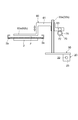
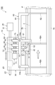
- FIG. 1 is a view showing a part of a bonding apparatus equipped with the substrate transfer apparatus according to the first embodiment
- FIG. 2 is a view showing the substrate transfer apparatus shown in FIG.
- the bonding apparatus 1 bonds a semiconductor die to a substrate F transported to a bonding stage 2.
- the substrate transport device 10 mounted on the bonding apparatus 1 transports the substrate F supplied from a loader side magazine (not shown) to the bonding stage 2, and after the semiconductor die is bonded to the substrate at the bonding stage, The substrate is transferred and stored in an unloader side magazine (not shown).
- the direction in which the substrate F is transported by the substrate transport apparatus 10 is referred to as a transport direction A.
- FIG. 3 is a diagram showing the configuration of the substrate F.
- the substrate F is a thin lead frame formed in a long rectangular sheet shape, and is formed of a glass epoxy resin.
- the substrate F is formed with a bonding region b to which a semiconductor die is bonded, and the plurality of bonding regions b collectively constitute one block B.
- 12 (4 rows ⁇ 4 columns) bonding regions b are configured as one block B.
- a plurality of blocks B are aligned along the longitudinal direction, and are arranged at equal intervals with a predetermined space S therebetween.
- a pair of rails 3 a and 3 b serving as a transport path for the substrate F extend along the transport direction A.
- the pair of rails 3a and 3b are disposed substantially the same as or slightly wider than the width of the substrate F, and are formed in a U-shape in which the recesses face each other in order to support both ends of the substrate F in the width direction. ing.
- the substrate F is placed on the inner lower surfaces of the rails 3a and 3b, and the movement in the width direction is restricted on the inner side surfaces of the rails 3a and 3b, and is transported in the transport direction A.
- the bonding stage 2 is arranged between the pair of rails 3a and 3b and spaced apart from the rails 3a and 3b by a predetermined distance, and the upper surface thereof is installed at the same height as the inner lower surface of the rails 3a and 3b. Has been.
- the bonding stage 2 has a plurality of suction ports (not shown). When bonding a semiconductor die to the substrate F, these suction ports are brought into a vacuum state (generating suction force), The conveyed substrate F is attracted to the bonding stage 2.
- a heater (not shown) for heating the substrate F to about 50 ° C. is provided below the bonding stage 2 so that the semiconductor die can be easily bonded to the substrate F.
- the bonding apparatus 1 is equipped with a substrate transfer device 10 for transferring the substrate F.
- the substrate transport apparatus 10 transports the substrate F in the transport direction A by moving in the transport direction A.
- two substrate transfer apparatuses 10 a and 10 b arranged along the transfer direction A (in series) are mounted on the bonding apparatus 1.
- two substrate transfer apparatuses 10a and 10b are mounted (in series) along the transfer direction A in order to shorten the bonding processing time.
- both have the same configuration, only one may be used. Three or more may be sufficient. For this reason, in the following description, unless otherwise specified, the substrate transfer device 10a and the substrate transfer device 10b will be collectively described as the substrate transfer device 10 without being separated.
- the substrate transport apparatus 10 has an X-axis table 30 that can be moved in the transport direction A by driving by the X-axis moving device 20 on the opposite side of the bonding stage 2 with respect to the rail 3a (upper side of the rail 3a in FIG. Is provided.
- the X-axis moving device 20 includes a motor 21 fixed to the bonding device 1, a ball screw 22 connected to the output shaft of the motor 21 and extending in the conveying direction A, and an X-axis table 30 fixed to the ball screw 22. It is comprised by the ball spline 23 used as a bearing. The movement of the X-axis table 30 in the transport direction A is performed by the ball spline 23 moving in the transport direction A due to the rotation of the ball screw 22 accompanying the rotational drive of the motor 21.
- the motor 21 is configured by a stepping motor or the like, and is a motor that can finely adjust the rotation angle, the number of rotations, and the like.
- FIG. 4 is a side view showing the configuration of the upper claw member and the lower claw member.
- the upper claw member 40 is attached to the X-axis table 30 so as to be vertically movable, and presses the substrate F from the upper surface. Therefore, the upper claw member 40 includes an arm portion 41 that is moved up and down by the driving device 70 and an upper claw portion 42 that is attached to the tip of the arm portion 41 and presses the substrate F.
- the arm portion 41 extends over the rail 3a from above and extends in a direction perpendicular to the transport direction A.
- One end portion of the arm portion 41 extends to the driving device 70, and the other end portion is the rail of the substrate F to be transported. It extends to the end on the 3a side.
- a roller 43 that is pivotally supported on a shaft facing the transport direction A is rotatably attached to one end of the arm portion 41.
- the arm portion 41 is inserted with a linear motion guide 31 erected in the vertical direction on the X-axis table 30, and can move up and down along the linear motion guide 31.
- the upper claw portion 42 is fixed to the other end portion of the arm portion 41 and is formed in an elongated plate shape extending in the transport direction A. And the upper nail
- the lower claw member 50 is attached to the X-axis table 30 so as to be movable up and down, and presses the substrate F from the lower surface.
- the lower claw member 50 includes an arm portion 51 that is moved up and down by the drive device 70 and a lower claw portion 52 that is attached to the tip of the arm portion 51 and presses the substrate F.
- the arm 51 extends from the lower side in the direction perpendicular to the transport direction A across the rail 3a, and its one end extends to the driving device 70 and the other end thereof is the rail of the substrate F to be transported. It extends to the end on the 3a side.
- a roller 53 that is pivotally supported by a shaft facing the transport direction A is rotatably attached to one end of the arm portion 51.
- the arm portion 51 is inserted with a linear motion guide 32 erected in the vertical direction on the X-axis table 30, and can move up and down along the linear motion guide 32.
- the lower claw portion 52 is fixed to the other end portion of the arm portion 51 and is formed in an elongated plate shape extending in the transport direction A. And the lower nail
- FIG. 5 is a side view showing the configuration of the substrate pressing member.
- the substrate pressing member 60 is attached to the X-axis table 30 so as to be movable up and down, and presses the substrate F against the bonding stage 2.
- the substrate pressing member 60 includes an arm portion 61 that is moved up and down by the driving device 70 and a pair of pressing portions 62a and 62b that are attached to the tip of the arm portion 61 and press the substrate F against the bonding stage 2. It is configured.
- the arm portion 61 extends over the rail 3a from above and extends in a direction perpendicular to the transport direction A.
- One end portion of the arm portion 61 extends to the driving device 70, and the other end portion is the rail of the substrate F to be transported. It extends to the end on the 3a side.
- a roller 63 that is pivotally supported on a shaft facing the transport direction A is rotatably attached to one end of the arm portion 61.
- the arm portion 61 is bifurcated from one end portion to the other end portion in the central portion, and the branched end portion has a branch width up to the interval of the blocks B formed on the substrate F. It has been spread.
- a pair of other end parts branched in the arm part 61 are arrange
- the arm portion 61 is inserted with linear motion guides 33a and 33b standing vertically in the X-axis table 30 at the center portion bifurcated, and is vertically moved along the linear motion guides 33a and 33b. It is possible to move.
- the pressing portions 62a and 62b are respectively fixed to the other branched ends of the arm portion 61, and are formed in an elongated plate shape extending in the direction perpendicular to the transport direction A along the bonding stage 2. Then, the pressing portions 62a and 62b move the substrate F along the direction perpendicular to the transport direction A on the lower surface thereof when the arm portion 61 moves down along the linear motion guides 33a and 33b. Press on.
- the driving device 70 is fixed to the X-axis table 30 to move the upper claw member 40, the lower claw member 50, and the substrate pressing member 60 up and down.
- the motor 71, a camshaft 72 connected to the output shaft of the motor 71 and extending in the transport direction A, and vertical movement cams 73 to 75 fitted into the camshaft 72 are configured.
- the motor 71 is configured by a stepping motor or the like, similar to the motor 21 of the X-axis moving device 20, and is a motor capable of finely adjusting the rotation angle, the number of rotations, and the like.
- the camshaft 72 is a shaft into which the vertical movement cams 73 to 75 are fitted and rotates these vertical movement cams 73 to 75 as a single body (synchronously).
- the vertical movement cam 73 is disposed at a position corresponding to the roller 43 of the upper claw member 40, and moves the upper claw member 40 up and down by its rotation.
- the roller 43 is urged against the vertical movement cam 73 by an urging means (not shown).
- the vertical movement cam 74 is arranged at a position corresponding to the roller 53 of the lower claw member 50, and moves the lower claw member 50 up and down by its rotation.
- the roller 53 is urged to the vertical movement cam 74 by an urging means (not shown).
- the vertical movement cam 75 is arranged at a position corresponding to each of the rollers 63 of the substrate pressing member 60, and moves the substrate pressing member 60 up and down by its rotation.
- the roller 63 is urged to the vertical movement cam 75 by an urging means (not shown).
- FIG. 6 is a cam curve diagram showing the shape of the vertical motion cam with respect to the rotation angle of the vertical motion cam.
- FIG. 6A is a cam curve diagram of the vertical motion cam that moves the substrate pressing member up and down.
- FIG. 6C shows a cam curve diagram of a vertically moving cam for moving the lower claw member up and down.
- the height of the vertically moving cams 73 and 74 when the substrate F is sandwiched (that is, the height of the upper claw member 40 and the lower claw member 50) is set to 0 mm, and the substrate F is pressed against the bonding stage 2.
- the height of the vertical movement cam 75 (that is, the height of the substrate pressing member 60) is set to 0 mm.
- the rotation angle of the camshaft 72 is ⁇
- the upper claw member 40, the lower claw member 50, and the substrate pressing member 60 move up and down as follows by the rotation of the vertical movement cams 73 to 75.
- the height of the upper claw member 40 is the second upper claw member position of 2.2 mm. Then, the upper claw member 40 is maintained at the second upper claw member position where the height of the upper claw member 40 is 2.2 mm over a rotation angle ⁇ of 0 ° to 30 °, and the upper claw member 40 is applied over a rotation angle ⁇ of 30 ° to 90 °. Is lowered from 2.2 mm to 0 mm to become the first upper claw member position, and the upper claw member 40 is maintained at the first upper claw member position where the height of the upper claw member 40 is 0 mm from 90 ° to 180 °.
- the height of the upper claw member 40 is lowered from 0 mm to -0.1 mm when the rotation angle ⁇ is 180 ° to 200 °, and the height of the upper claw member 40 is increased from the rotation angle ⁇ to 200 ° to 260 °. Decreases from ⁇ 0.1 mm to ⁇ 0.6 mm, the rotation angle ⁇ increases from 260 ° to 330 °, the height of the upper claw member 40 increases from ⁇ 0.6 mm to 2.2 mm, and the second upper claw member Returning to the position, when the rotation angle ⁇ is 330 ° to 360 °, the height is 2. It is maintained at the second upper claw member position in mm.
- the lower claw member 50 is at the second lower claw member position where the height of the lower claw member 50 is ⁇ 1.3 mm. Then, when the rotation angle ⁇ is 0 ° to 60 °, the height of the lower claw member 50 is increased from ⁇ 1.3 mm to 0 mm to become the first lower claw member position, and when the rotation angle ⁇ is 60 ° to 180 °, The height of the lower claw member 50 is maintained at the first lower claw member position of 0 mm, the rotation angle ⁇ is lowered from 180 ° to 200 °, and the height of the lower claw member 50 is lowered from 0 mm to ⁇ 0.1 mm. When the rotation angle ⁇ is 200 ° to 360 °, the height of the lower claw member 50 is lowered from ⁇ 0.1 mm to ⁇ 1.3 mm and returned to the second lower claw member position.
- the height of the substrate pressing member 60 is the second substrate pressing member position of 6 mm.
- the substrate pressing member 60 is maintained at the second substrate pressing member position where the rotation angle ⁇ is 0 ° to 30 °, and the height of the substrate pressing member 60 is increased when the rotation angle ⁇ is 30 ° to 135 °. Is lowered to 0 mm to become the first substrate pressing member position, and the rotation angle ⁇ is maintained at the first substrate pressing member position where the height of the substrate pressing member 60 is 0 mm from 135 ° to 260 °.
- the height of the substrate pressing member 60 increases from 0 mm to 6 mm and returns to the second substrate pressing member position, and the height of the substrate pressing member 60 increases from the rotation angle ⁇ to 330 ° to 360 °. Is maintained at the second substrate pressing member position of 6 mm.
- the rotation angle ⁇ is in the range of 30 ° to 135 °
- the height of the substrate pressing member 60 is the third substrate pressing member position between the first substrate pressing member position and the second substrate pressing member position.
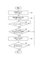
- FIG. 7 is a flowchart for explaining the operation of the substrate transfer apparatus.
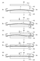
- FIG. 8 is a diagram for explaining the substrate acquisition operation of the substrate transfer apparatus.
- the motor 71 of the driving device 70 is rotationally driven to rotate the rotation angle ⁇ of the camshaft 72 to 0 ° (see FIG. 8A).
- the upper claw member 40 is at the second upper claw member position
- the lower claw member 50 is at the second lower claw member position
- the substrate pressing member 60 is at the second substrate pressing member position.
- the motor 21 of the X-axis moving device 20 is rotationally driven so that the pressing portions 62a and 62b of the substrate pressing member 60 correspond to the positions corresponding to the spaces S arranged forward and backward in the transport direction A of the block B to be bonded.
- the X-axis table 30 is moved until it becomes.
- the substrate F is heated to about 50 ° C. by the heater installed below the bonding stage 2, the substrate F is bent and is bent in a convex shape.
- the motor 71 of the driving device 70 is driven to rotate, and the rotation angle ⁇ of the camshaft 72 is rotated to 135 °.
- the substrate pressing member 60 descends within the range of the third substrate pressing member position when the rotation angle ⁇ is 90 ° to 135 ° (see FIG. 8D). As a result, the substrate pressing member 60 gradually presses the substrate F against the bonding stage 2. When the rotation angle ⁇ reaches 135 °, the substrate pressing member 60 becomes the first substrate pressing member position. Therefore, in addition to the substrate F being sandwiched between the upper claw member 40 and the lower claw member 50, the substrate pressing member 60 The substrate F is completely pressed against the bonding stage 2, and the bent substrate F is corrected into a flat plate shape (see FIG. 8E).
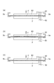
- FIG. 9 is a diagram for explaining the substrate transfer operation of the substrate transfer apparatus.
- the motor 71 of the driving device 70 is rotationally driven to rotate the rotational angle ⁇ of the camshaft 72 to any angle in the range of 90 ° to 135 ° ( (See FIGS. 9A and 9B).
- the substrate pressing member 60 slightly rises to the third substrate pressing member position.
- the pressing of the substrate F against the bonding stage 2 by the pressing portions 62a and 62b of the substrate pressing member 60 is alleviated, so that the flexure of the substrate F is slightly restored, and the space between the substrate F and the bonding stage 2 is reduced. A gap is created.
- the motor 21 of the X-axis moving device 20 is rotationally driven, and the X-axis table 30 is moved in the transport direction A until the bonding area b to be bonded becomes the bonding position.
- the motor 71 of the driving device 70 is rotationally driven to rotate the rotational angle ⁇ of the camshaft 72 to 135 ° (see FIG. 9C).
- the substrate pressing member 60 completely presses the substrate F against the bonding stage 2, so that the bent substrate F is corrected into a flat plate shape.
- the substrate transfer device 10 stands by until the bonding die 1 bonds the semiconductor die to the bonding region b of the substrate F (step S3).
- the substrate transfer apparatus 10 determines whether or not the semiconductor die is bonded to all the bonding areas b in the block B (step S4).
- step S2 If the semiconductor die is not bonded to all the bonding regions b in the block B, the process returns to step S2 and the above operation is repeated.
- FIG. 10 is a diagram for explaining the substrate holding operation of the substrate transfer apparatus.
- the motor 71 of the driving device 70 is rotationally driven, and the rotation angle ⁇ of the camshaft 72 is changed from 135 ° to 0 ° (or from 135 ° to 30 ° to 0 °). Reverse rotation (° range).
- the rotation angle ⁇ is 60 ° to 0 ° (or from 60 ° to 30 ° to 0 °)
- the upper claw member 40 is raised, the lower claw member 50 is lowered from the first lower claw member position, and the substrate is pressed.
- the member 60 rises (see FIG. 10D).
- the rotation angle ⁇ reaches 0 °
- the upper claw member 40 is at the second upper claw member position
- the lower claw member 50 is at the second lower claw member position
- the substrate pressing member 60 is at the second substrate pressing member position.
- the motor 21 of the X-axis moving device 20 is rotationally driven so that the pressing portions 62a and 62b of the substrate pressing member 60 sandwich the block B to be bonded next, and are arranged forward and backward in the transport direction A of the block B.
- the X-axis table 30 is moved until it reaches a position corresponding to the space S.
- the motor 71 of the driving device 70 is rotationally driven to rotate the rotational angle ⁇ of the camshaft 72 to 135 °, and the upper claw member 40 and the lower claw member 50
- the substrate F is sandwiched and the substrate F is pressed against the bonding stage 2 by the substrate pressing member 60 (see FIGS. 8A to 8E).
- the substrate transfer apparatus 10 repeats the above operation until the semiconductor die is bonded to all the blocks B of the substrate F (step S6).
- the upper claw member 40 and the lower claw member 50 are driven by the driving device 70 to sandwich the substrate F from the upper and lower surfaces, and the upper claw is moved by the X-axis moving device 20.
- the substrate F can be transported in the transport direction A.
- the substrate pressing member 60 is driven by the driving device 70 to bring the substrate F into the bonding stage 2. By pressing, the substrate F bent by heat or the like can be corrected into a flat plate shape.
- the X-axis moving device 20 moves the upper claw member 40, the lower claw member 50, and the substrate pressing member 60 together in the transport direction A, so that the position of the substrate F pressed by the substrate pressing member 60 is the substrate F. Therefore, the semiconductor die or the like can be stably bonded to the substrate F.
- substrate pressing member 60 can be moved up and down by the single motor 71, the number of parts of the board
- the upper claw member 40, the lower claw member 50, and the substrate are moved by the single motor 71 by using the vertical movement cams 73 to 75 that move the upper claw member 40, the lower claw member 50, and the substrate pressing member 60 up and down.
- the pressing member 60 can be moved up and down independently.
- the upper claw member 40, the lower claw member 50, and the substrate pressing member 60 are moved to three different positional relationships by a single motor 71.
- the positional relationship between the upper claw member 40 and the lower claw member 50 and the substrate pressing member 60 can be changed in accordance with the conveyance or bonding of the substrate F.
- the substrate When bonding is performed to the substrate F, the substrate is sandwiched between the upper claw member 40 and the lower claw member 50 by rotating the rotation angle ⁇ of the vertical movement cams 73 to 75 to 135 °, and the substrate pressing member. Since the substrate F is pressed against the bonding stage 2 by 60, the bent substrate F can be corrected into a flat plate shape, and a semiconductor die or the like can be appropriately bonded to the substrate F.
- the upper claw member 40 is rotated by rotating the vertical movement cams 73 to 75 to 0 ° (or a range of 30 ° to 0 °).
- the sandwiching of the substrate F by the lower claw member 50 can be released, and the pressing of the substrate F to the bonding stage 2 by the substrate pressing member 60 can be released. Therefore, the upper claw member 40, the lower claw member 50, and the substrate pressing member The substrate F can be held by the upper claw member 40 and the lower claw member 50 without the interference of the substrate 60 with the substrate F.
- the upper claw member 40 and the lower claw member 50 are rotated by rotating the vertical movement cams 73 to 75 in the range of 90 ° to 135 °.
- the pressing of the substrate F to the bonding stage 2 by the substrate pressing member 60 can be released.
- the contact resistance between the substrate F and the bonding stage 2 is reduced, it is possible to reduce rubbing of the substrate F due to the contact with the bonding stage 2 when the substrate F is transported.
- the movement distance of the substrate pressing member 60 is shortened. Therefore, the substrate F can be transported quickly.
- FIG. 11 is a view showing a substrate transfer apparatus according to the second embodiment.
- the substrate transport apparatus 100 according to the second embodiment is basically the same as the substrate transport apparatus 10 according to the first embodiment.
- the substrate transport apparatus 100 is different from the substrate transport apparatus 10 only in that an auxiliary substrate pressing member 80 is added. For this reason, below, only the point which is different from 1st Embodiment is demonstrated, and other description is abbreviate
- an auxiliary substrate pressing member 80 is attached to the substrate pressing member 60 in the substrate transport apparatus 100.
- the auxiliary substrate pressing member 80 presses the bonded substrate F against the bonding stage 2.
- the auxiliary board pressing member 80 includes an auxiliary arm portion 81 and an auxiliary pressing portion 82.
- the auxiliary arm portion 81 has one end attached to the center portion of the arm portion 61 of the substrate pressing member 60 on the opposite side of the bonding stage 2 with respect to the rail 3a.
- the auxiliary arm portion 81 extends forward in the transport direction A from the arm portion 61 and is bent toward the rail 3a side.
- the auxiliary arm portion 81 further extends in the direction perpendicular to the transport direction A across the rail 3a from above, and the other end portion extends to the end portion on the rail 3a side of the substrate F to be transported.
- the other end portion of the auxiliary arm portion 81 is arranged in the conveying direction A so as to be separated from the pressing portion 62a by the length of one block B.
- the other end portion of the auxiliary arm portion 81 corresponds to the position of the next space S in the transport direction A of the space S of the substrate F pressed by the pressing portion 62a. Since the auxiliary arm portion 81 is connected to the arm portion 61, it moves up and down as the arm portion 61 moves up and down.
- the auxiliary pressing portion 82 is fixed to the other end portion of the auxiliary arm portion 81 and is formed in an elongated plate shape extending in the direction perpendicular to the transport direction A along the bonding stage 2. Then, the auxiliary pressing unit 82 presses the substrate F against the bonding stage 2 along the direction perpendicular to the transport direction A on the lower surface thereof when the auxiliary arm unit 81 descends as the arm unit 61 descends. .
- the auxiliary substrate pressing member 80 is also lowered as the substrate pressing member 60 is lowered. To do. Then, as shown in FIG. 3, the auxiliary pressing portion 82 of the auxiliary substrate pressing member 80 presses the space S one forward in the transport direction A of the space S pressed by the pressing portion 62 a of the substrate pressing member 60. Therefore, the space S on both sides in the transport direction A of the bonded block B is pressed against the bonding stage 2 by the auxiliary pressing portion 82 of the pressing portion of the auxiliary substrate pressing member 80 and the pressing portion 62a of the substrate pressing member 60. The block B is corrected into a flat plate shape.
- the substrate transfer apparatus 100 in addition to the above-described effects, the following effects are further obtained. That is, immediately after the semiconductor die is bonded to the substrate F, the bending of the substrate F due to heat or the like is not sufficiently restored, and the bonding strength between the semiconductor die and the substrate F is weak. Therefore, an auxiliary substrate pressing member 80 extending from the arm portion 61 in the substrate pressing member 60 in the transport direction A is provided, and the substrate F is pressed against the bonding stage 2 by the auxiliary substrate pressing member 80, whereby the semiconductor die is bonded to the block. B can be corrected into a flat plate shape, and peeling of the bonded semiconductor die from the substrate F can be suppressed.
- the movement of the upper claw member 40, the lower claw member 50, and the substrate pressing member 60 in the transport direction A is performed by moving the upper claw member 40, the lower claw member 50, and the substrate pressing member 60 to the X-axis table 30.
- this is performed by driving the X-axis table 30 with the X-axis moving device 20, the upper claw member 40, the lower claw member 50, and the substrate pressing member 60 are integrally moved in the transport direction A. If it is possible, it may be moved by any configuration and means.
- the vertical movement of the upper claw member 40, the lower claw member 50, and the board pressing member 60 is caused by the vertical movement cams 73 to 73 at positions corresponding to the upper claw member 40, the lower claw member 50, and the board pressing member 60. 75, and a single motor 71 rotates these vertical cams 73 to 75.
- the upper claw member 40, the lower claw member 50, and the substrate pressing member 60 are moved up and down independently. As long as it can be moved, it may be moved up and down by any configuration and means.
- the vertical movement cams 73 to 75 have been described as having the shape shown in FIG. 6, but the shape in which the upper claw member 40, the lower claw member 50, and the substrate pressing member 60 are moved up and down independently. Any shape can be used.
- the pressing unit 62 and the auxiliary pressing unit 82 have been described as extending in the direction perpendicular to the transport direction A along the bonding stage 2, but the substrate F is pressed against the bonding stage 2.
- Any shape / structure is possible as long as it is possible.
- it may be a shape bent in an L shape along the bonding stage 2 or a square shape surrounding the periphery of one or a plurality of bonding regions b or one or a plurality of blocks B.
- the present invention can be used in a bonding apparatus for bonding a semiconductor die to a substrate.
Landscapes
- Engineering & Computer Science (AREA)
- Mechanical Engineering (AREA)
- Die Bonding (AREA)
- Supply And Installment Of Electrical Components (AREA)
- Wire Bonding (AREA)
- Pressure Welding/Diffusion-Bonding (AREA)
Abstract
Description
この基板搬送装置によれば、上爪部材、下爪部材及び基板押付部材を上下動させる上下動カムを用いることで、単一の回転駆動源により、上爪部材、下爪部材及び基板押付部材を独立して上下動させることができる。しかも、第1回転角度範囲、第2回転角度範囲及び第3回転角度範囲を有する上下動カムを用いることで、単一の回転駆動源により、上爪部材及び下爪部材と基板押付部材とを、異なる3つの位置関係に移動させることができ、基板の搬送やボンディングなど応じて、上爪部材及び下爪部材と基板押付部材との位置関係を変えることができる。
を含む。
図1は、第1の実施形態に係る基板搬送装置を搭載したボンディング装置の一部を示した図であり、図2は、図1に示す基板搬送装置を示した図である。
次に、図11を参照して、第2の実施形態に係る基板搬送装置ついて説明する。
Claims (7)
- ボンディングステージ上でボンディングが行われる基板を搬送方向に搬送する基板搬送装置であって、
基板を上下面から挟み込む上爪部材及び下爪部材と、
基板をボンディングステージに押し付ける基板押付部材と、
上爪部材、下爪部材及び基板押付部材を一体で搬送方向に移動させる移動装置と、
上爪部材、下爪部材及び基板押付部材を上下動させる駆動装置と、
を含む基板搬送装置。 - 駆動装置は、
上爪部材、下爪部材及び基板押付部材を上下動させる上下動カムと、
上下動カムを回転させる単一の回転駆動源と、
を含み、
上下動カムは、
上爪部材及び下爪部材が基板を挟み込む第1爪部材位置に上爪部材及び下爪部材を移動装置により移動させ、且つ、基板押付部材が基板をボンディングステージに押し付ける第1基板押付部材位置に基板押付部材を移動させる第1回転角度範囲と、
上爪部材及び下爪部材が基板を挟み込まない第2爪部材位置に上爪部材及び下爪部材を移動装置により移動させ、且つ、基板押付部材が基板をボンディングステージに押し付けない第2基板押付部材位置に基板押付部材を移動させる第2回転角度範囲と、
第1爪部材位置に上爪部材及び下爪部材を移動装置により移動させ、第1基板押付部材位置と第2基板押付部材位置との間の第3基板押付部材位置に基板押付部材を移動させる第3回転角度範囲と、を含む請求項1に記載の基板搬送装置。 - 回転駆動源は、基板にボンディングが行われる場合、上下動カムを第1回転角度範囲に回転させる請求項2に記載の基板搬送装置。
- 回転駆動源は、上爪部材及び下爪部材により基板をつかみ替える場合、上下動カムを第2回転角度範囲に回転させる請求項2に記載の基板搬送装置。
- 回転駆動源は、上爪部材及び下爪部材により基板を搬送する場合、上下動カムを第3回転角度範囲に回転させる請求項2に記載の基板搬送装置。
- 基板押付部材の搬送方向前方に配置され、上下動して基板をボンディングステージに押し付ける補助基板押付部材を更に含み、
駆動装置は、補助基板押付部材を基板押付部材と同期して上下動させる請求項1に記載の基板搬送装置。 - ボンディングステージ上でボンディングが行われる基板を搬送方向に搬送する基板搬送方法であって、
搬送方向に搬送される基板にボンディングが行われるボンディングステージと、上下動して基板を上下面から挟み込む上爪部材及び下爪部材と、上下動して基板をボンディングステージに押し付ける基板押付部材と、上爪部材、下爪部材及び基板押付部材を一体で搬送方向に移動させる移動装置と、上爪部材、下爪部材及び基板押付部材を上下動させる駆動装置と、を有する基板搬送装置を用意するステップと、
基板にボンディングが行われる際に、駆動装置により、基板を挟み込む第1爪部材位置に上爪部材及び下爪部材を移動装置により移動させ、基板をボンディングステージに押し付ける第1基板押付部材位置に基板押付部材を移動させるボンディング準備動作ステップと、
上爪部材及び下爪部材により基板をつかみ替える際に、駆動装置により、基板を挟み込まない第2爪部材位置に上爪部材及び下爪部材を移動装置により移動させ、基板をボンディングステージに押し付けない第2基板押付部材位置に基板押付部材を移動させる持ち替え動作ステップと、
上爪部材及び下爪部材により基板を搬送する際に、第1爪部材位置に上爪部材及び下爪部材を移動装置により移動させ、第1基板押付部材位置と第2基板押付部材位置との間の第3基板押付部材位置に基板押付部材を移動させる搬送ステップと、
を含む基板搬送方法。
Priority Applications (2)
| Application Number | Priority Date | Filing Date | Title |
|---|---|---|---|
| KR1020117003652A KR101096485B1 (ko) | 2008-10-16 | 2009-04-28 | 기판 반송 장치 및 기판 반송 방법 |
| CN200980140251.7A CN102177574B (zh) | 2008-10-16 | 2009-04-28 | 基板运送装置及基板运送方法 |
Applications Claiming Priority (2)
| Application Number | Priority Date | Filing Date | Title |
|---|---|---|---|
| JP2008-267491 | 2008-10-16 | ||
| JP2008267491A JP4369522B1 (ja) | 2008-10-16 | 2008-10-16 | 基板搬送装置及び基板搬送方法 |
Publications (1)
| Publication Number | Publication Date |
|---|---|
| WO2010044287A1 true WO2010044287A1 (ja) | 2010-04-22 |
Family
ID=41443802
Family Applications (1)
| Application Number | Title | Priority Date | Filing Date |
|---|---|---|---|
| PCT/JP2009/058396 Ceased WO2010044287A1 (ja) | 2008-10-16 | 2009-04-28 | 基板搬送装置及び基板搬送方法 |
Country Status (4)
| Country | Link |
|---|---|
| JP (1) | JP4369522B1 (ja) |
| KR (1) | KR101096485B1 (ja) |
| CN (1) | CN102177574B (ja) |
| WO (1) | WO2010044287A1 (ja) |
Families Citing this family (2)
| Publication number | Priority date | Publication date | Assignee | Title |
|---|---|---|---|---|
| CN107520280B (zh) * | 2017-09-19 | 2023-10-20 | 中国建筑材料工业建设西安工程有限公司 | 一种控制板喂机槽板变形的动态校正装置 |
| JP7213602B2 (ja) * | 2021-01-28 | 2023-01-27 | 株式会社新川 | 半導体装置の製造装置、および、基板の清掃方法 |
Citations (5)
| Publication number | Priority date | Publication date | Assignee | Title |
|---|---|---|---|---|
| JPS5681945A (en) * | 1979-12-07 | 1981-07-04 | Hitachi Ltd | Assembling device |
| JPS5958830A (ja) * | 1982-09-28 | 1984-04-04 | Shinkawa Ltd | ボンダ−用ワ−ク加熱装置 |
| JPS6080231A (ja) * | 1983-10-07 | 1985-05-08 | Tokyo Sokuhan Kk | 半導体素子のボンデイング装置におけるリ−ドフレ−ムの自動送り位置決め機構 |
| JPH0661273A (ja) * | 1992-08-06 | 1994-03-04 | Mitsubishi Electric Corp | リードフレーム処理方法及びそのための装置 |
| JP2004356354A (ja) * | 2003-05-29 | 2004-12-16 | Shinkawa Ltd | ワイヤボンディング装置用フレーム固定装置 |
-
2008
- 2008-10-16 JP JP2008267491A patent/JP4369522B1/ja not_active Expired - Fee Related
-
2009
- 2009-04-28 KR KR1020117003652A patent/KR101096485B1/ko not_active Expired - Fee Related
- 2009-04-28 WO PCT/JP2009/058396 patent/WO2010044287A1/ja not_active Ceased
- 2009-04-28 CN CN200980140251.7A patent/CN102177574B/zh active Active
Patent Citations (5)
| Publication number | Priority date | Publication date | Assignee | Title |
|---|---|---|---|---|
| JPS5681945A (en) * | 1979-12-07 | 1981-07-04 | Hitachi Ltd | Assembling device |
| JPS5958830A (ja) * | 1982-09-28 | 1984-04-04 | Shinkawa Ltd | ボンダ−用ワ−ク加熱装置 |
| JPS6080231A (ja) * | 1983-10-07 | 1985-05-08 | Tokyo Sokuhan Kk | 半導体素子のボンデイング装置におけるリ−ドフレ−ムの自動送り位置決め機構 |
| JPH0661273A (ja) * | 1992-08-06 | 1994-03-04 | Mitsubishi Electric Corp | リードフレーム処理方法及びそのための装置 |
| JP2004356354A (ja) * | 2003-05-29 | 2004-12-16 | Shinkawa Ltd | ワイヤボンディング装置用フレーム固定装置 |
Also Published As
| Publication number | Publication date |
|---|---|
| JP4369522B1 (ja) | 2009-11-25 |
| KR20110028398A (ko) | 2011-03-17 |
| JP2010098114A (ja) | 2010-04-30 |
| KR101096485B1 (ko) | 2011-12-20 |
| CN102177574A (zh) | 2011-09-07 |
| CN102177574B (zh) | 2013-05-01 |
Similar Documents
| Publication | Publication Date | Title |
|---|---|---|
| TWI373813B (ja) | ||
| JP6121384B2 (ja) | 製造装置及び製造方法 | |
| KR100244688B1 (ko) | 웨이퍼 반송장치 | |
| WO2009122711A1 (ja) | 部品実装装置および方法 | |
| CN108237353B (zh) | 端焊机 | |
| CN113683297A (zh) | 一种全自动开片系统 | |
| JP2011056631A (ja) | テーブル昇降装置 | |
| WO2009110427A1 (ja) | 搬送装置 | |
| JP4369522B1 (ja) | 基板搬送装置及び基板搬送方法 | |
| KR20190115702A (ko) | 기판 절단 장치 | |
| KR101071265B1 (ko) | 디스플레이 패널 이송 유닛 및 이를 갖는 디스플레이 패널 가공 장치 | |
| TWI343610B (en) | Bonding device and a bonding system comprising this | |
| JP4854256B2 (ja) | パネル処理装置及び処理方法 | |
| JP4943936B2 (ja) | 電子部品の実装装置及び実装方法 | |
| JP2011035118A (ja) | Pcb実装処理装置及びpcb実装処理方法 | |
| JP5424969B2 (ja) | 基板の搬送装置及び搬送方法 | |
| JP4576268B2 (ja) | テープ貼込装置 | |
| TW201401395A (zh) | 電子零件之安裝裝置及安裝方法 | |
| JP4197171B2 (ja) | 電子部品実装機 | |
| JP2005259729A (ja) | 液晶セルのtab搭載装置及びその方法並びに液晶ディスプレイ | |
| JP4453494B2 (ja) | シート貼り付け装置及びシート貼り付け方法 | |
| JP2003273591A (ja) | 基板固定方法及び基板固定装置、並びにこれを用いた部品実装装置 | |
| CN113013051B (zh) | 电子元件作业机构及其应用的作业设备 | |
| JP4302252B2 (ja) | 表紙貼付け成形装置 | |
| KR20190115701A (ko) | 기판 절단 장치 |
Legal Events
| Date | Code | Title | Description |
|---|---|---|---|
| WWE | Wipo information: entry into national phase |
Ref document number: 200980140251.7 Country of ref document: CN |
|
| 121 | Ep: the epo has been informed by wipo that ep was designated in this application |
Ref document number: 09820465 Country of ref document: EP Kind code of ref document: A1 |
|
| ENP | Entry into the national phase |
Ref document number: 20117003652 Country of ref document: KR Kind code of ref document: A |
|
| NENP | Non-entry into the national phase |
Ref country code: DE |
|
| 122 | Ep: pct application non-entry in european phase |
Ref document number: 09820465 Country of ref document: EP Kind code of ref document: A1 |