WO2010035537A1 - 光走査装置、画像表示装置及び光走査装置の駆動方法 - Google Patents
光走査装置、画像表示装置及び光走査装置の駆動方法 Download PDFInfo
- Publication number
- WO2010035537A1 WO2010035537A1 PCT/JP2009/056242 JP2009056242W WO2010035537A1 WO 2010035537 A1 WO2010035537 A1 WO 2010035537A1 JP 2009056242 W JP2009056242 W JP 2009056242W WO 2010035537 A1 WO2010035537 A1 WO 2010035537A1
- Authority
- WO
- WIPO (PCT)
- Prior art keywords
- waveform
- unit
- waveform information
- drive
- ringing
- Prior art date
- Legal status (The legal status is an assumption and is not a legal conclusion. Google has not performed a legal analysis and makes no representation as to the accuracy of the status listed.)
- Ceased
Links
Images







Classifications
-
- G—PHYSICS
- G02—OPTICS
- G02B—OPTICAL ELEMENTS, SYSTEMS OR APPARATUS
- G02B26/00—Optical devices or arrangements for the control of light using movable or deformable optical elements
- G02B26/08—Optical devices or arrangements for the control of light using movable or deformable optical elements for controlling the direction of light
- G02B26/0816—Optical devices or arrangements for the control of light using movable or deformable optical elements for controlling the direction of light by means of one or more reflecting elements
- G02B26/0833—Optical devices or arrangements for the control of light using movable or deformable optical elements for controlling the direction of light by means of one or more reflecting elements the reflecting element being a micromechanical device, e.g. a MEMS mirror, DMD
- G02B26/085—Optical devices or arrangements for the control of light using movable or deformable optical elements for controlling the direction of light by means of one or more reflecting elements the reflecting element being a micromechanical device, e.g. a MEMS mirror, DMD the reflecting means being moved or deformed by electromagnetic means
-
- G—PHYSICS
- G02—OPTICS
- G02B—OPTICAL ELEMENTS, SYSTEMS OR APPARATUS
- G02B26/00—Optical devices or arrangements for the control of light using movable or deformable optical elements
- G02B26/08—Optical devices or arrangements for the control of light using movable or deformable optical elements for controlling the direction of light
- G02B26/10—Scanning systems
- G02B26/105—Scanning systems with one or more pivoting mirrors or galvano-mirrors
Definitions
- the present invention relates to an optical scanning device used for scanning a light beam.
- the present invention can be applied to an image display apparatus that forms a projection image by scanning a light beam two-dimensionally.
- the optical scanning device is used as an optical scanner for a copying machine or a printing machine, or as an optical scanner for a projection device.
- FIG. 11A is a schematic diagram showing how this type of optical scanning device 100 performs optical scanning.
- a reflective surface is formed on the surface of the reflective portion 101.
- a light beam is irradiated from the light source 103 onto the reflection surface of the reflection unit 101.
- a coil (not shown) is formed on the back surface of the reflecting portion 101 where the reflecting surface is not formed, and a magnet is installed around the reflecting portion 101.
- Lorentz force is applied to the current path according to Fleming's left-hand rule, and the reflecting portion swings about the swing axis.
- the light beam incident on the reflecting surface by the swinging of the reflecting portion is scanned as scanning light when reflected.
- the light source 103 is supplied with a drive signal whose intensity is modulated in accordance with, for example, an image signal from the drive circuit 102, and repeats turning on and off. Drawing can be performed with scanning light reflected by the reflection unit 101 by driving the reflection unit 101 in synchronization with the turning on and off of the light source 103.
- FIG. 11B shows an example of a drive signal for driving the reflection unit 101, and shows vertical scanning when an image is projected by two-dimensional scanning.
- the horizontal axis represents time and the vertical axis represents current amplitude.
- the drive signal has a periodic shape whose amplitude is sawtooth with respect to time.
- FIG. 11C shows the swinging state of the reflection unit 101.
- the horizontal axis represents time
- the vertical axis represents the mirror angle of the reflecting surface. The mirror angle periodically oscillates in a sawtooth shape with reference to a horizontal state in which no drive signal is given to the reflecting portion.
- the mirror angle is superimposed with ringing consisting of minute vibrations as shown in the inset indicated by the arrow.
- the scanning light is also superimposed with the period of this minute vibration, and unevenness in the scanning speed is superimposed.
- unevenness in density appears in the scanning lines of the displayed image, thereby degrading the image quality.
- the ringing shown in the inset of FIG. 11C occurs for the following reasons.
- the reflection unit 101 is supported by a support unit.
- a restoring force that restores the rotation works due to the torsional elasticity of the supporting portion that supports the reflecting portion 101. Therefore, it has a natural vibration determined by the moment of inertia of the reflecting portion 101 and the torsional elasticity of the support portion. Further, even if the structure is not as shown in FIG. 11A, if a restoring force that restores the rotation mechanically, electrically, or magnetically is applied to the rotation of the reflecting portion 101, a natural vibration is generated.
- the drive signal increases linearly during the scanning period for displaying an image, and shifts to a return period during which no image is displayed.
- the drive signal changes abruptly when the transition is made from the return period to the scanning period. That is, the drive signal changes rapidly near the top of the sawtooth shape.
- This sudden change in the drive signal gives an impact to the reflecting portion 101, and a specific resonance vibration is induced in the reflecting portion 101.
- resonance vibration occurs in the reflecting portion 101, it continues for a while unless a drive signal is applied to cancel the resonance vibration.
- the resonance vibration lasts for one frame period or more, causing the quality of the projected image to deteriorate.
- Patent Document 1 describes that this type of ringing, which occurs when a sawtooth drive current is applied to a galvano mirror, is reduced by applying a stepped pulse during the drive current recovery period. . It is described that ringing can be suppressed by appropriately selecting a stepped pulse width and pulse height.
- Patent Document 2 in a system for driving a galvano-type scanner, a plurality of drive patterns for driving the galvano-type scanner are stored in a ROM, and a preset drive pattern is used in actual use. It is described that even when a deviation occurs, it is possible to cope with the deviation by selecting a driving pattern, and there is no need to connect an expensive command generator to the outside. JP 54-89673 A JP 2005-338450 A
- any one of a plurality of driving waveforms is obtained. It is an object of the present invention to provide an optical scanning device, an image display device, and an optical scanning device driving method capable of controlling the ringing amount to a predetermined value or less by selecting.
- a reflection unit that scans a light beam by oscillation and a drive that generates a drive waveform for oscillating the reflection unit.
- a waveform information storage unit for storing a plurality of waveform information used for generating the drive waveform, and selecting one waveform information from the plurality of waveform information, and selecting a drive waveform based on the selected waveform information
- a plurality of waveform information is sequentially given to the driving unit, and waveform information in which the detected ringing amount is smaller than a predetermined value is selected.
- waveform information that changes over time is stored in advance, the amount of ringing that is superimposed on the swing of the reflector is detected, and waveform information that reduces the amount of ringing is selected.
- the ringing amount of the reflecting portion can be driven smaller than a predetermined value.
- the driving waveform may have a sawtooth or triangular wave periodic shape
- the detection unit may detect a ringing amount in an effective scanning period of the reflection unit.
- the detection unit may include a piezoelectric element for detecting the swing of the reflection unit.
- the waveform information includes a frequency component such that a component of a specific frequency is suppressed, and the waveform information storage unit stores a plurality of waveform information having different specific frequencies.
- the drive waveform setting unit may sequentially provide waveform information with different specific frequencies to the drive unit.
- Such a configuration can effectively reduce the ringing associated with the natural vibration of the reflecting portion.
- the waveform information includes a parameter value corresponding to a physical quantity that affects the vibration of the reflecting section
- the drive waveform setting section includes a plurality of parameter values in which the physical quantity changes roughly. And sequentially providing a plurality of waveform information corresponding to the set parameter values to the drive unit, specifying a parameter value in which the detected ringing amount is smaller than the predetermined value, and specifying the specified
- a parameter value in which the physical quantity changes finely is set, waveform information corresponding to the set parameter value is given to the drive unit, and waveform information that minimizes the detected ringing amount is obtained. You may make it the structure to select.
- the drive waveform is first roughly changed, the parameter value whose ringing amount is smaller than the predetermined value is specified, the drive waveform is further changed, and the drive waveform that minimizes the ringing amount is selected.
- the ringing amount of the reflecting portion can be suppressed quickly and to the minimum.
- the drive waveform setting unit sets a plurality of parameter values in which the physical quantity changes finely, and sets a plurality of waveform information corresponding to the set plurality of parameter values to the drive unit. You may make it the structure given sequentially.
- a low-speed optical scanning device comprising the optical scanning device, a high-speed optical scanning device, a light source that generates an intensity-modulated light beam based on an image signal and irradiates the optical scanning device, and a scanning from the optical scanning device.
- An image display apparatus including a projection lens system for projecting a light beam.
- waveform information when it changes over time is stored in advance, the amount of ringing superimposed on the swing of the reflecting portion is detected, and the waveform information stored in advance is selected. Since the ringing amount of the reflecting portion can be made smaller than a predetermined value, it is possible to prevent the quality of the projected image from being deteriorated with time.
- a drive unit that generates a drive waveform for swinging the reflection unit, a waveform information storage unit that stores a plurality of waveform information used to generate the drive waveform, and one waveform information from the plurality of waveform information
- a drive waveform setting unit that selects and sets the drive waveform by applying the selected waveform information to the drive unit, and a detection unit that detects a ringing amount based on vibration superimposed on the swing of the reflection unit.
- the drive waveform setting unit reads a plurality of waveform information stored in the waveform information storage unit, and supplies the read waveform information to the drive unit to cause the reflection unit to
- the step of oscillating and the ringing amount detected by the detection unit are compared with a predetermined value, and the waveform information when the detected ringing amount becomes smaller than the predetermined value is selected.
- flop were and driving the reflecting portion of the selected waveform information set to the drive unit, and a driving method for an optical scanning device comprising a.
- a drive unit that generates a drive waveform for swinging the reflection unit, a waveform information storage unit that stores a plurality of waveform information used for generating the drive waveform, and a plurality of waveform information are used.
- a drive waveform setting unit that selects one waveform information and sets a drive waveform based on the selected waveform information, and a detection unit that detects a ringing amount based on unnecessary vibration included in the swing of the reflection unit,
- the drive waveform setting unit sequentially supplies the plurality of waveform information stored in the waveform information storage unit to the drive unit, and selects the waveform information in which the detected ringing amount is smaller than a predetermined value.
- the waveform information when it changes over time is stored in advance, the amount of ringing superimposed on the swing of the reflecting portion is detected, the waveform information that reduces the ringing amount is selected, and the waveform of the reflecting portion is selected.
- the ringing amount can be driven smaller than a predetermined value.
- 1 is a basic configuration diagram of an optical scanning device according to an embodiment of the present invention.
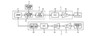
- 1 is a configuration diagram of an optical scanning device according to an embodiment of the present invention. It is explanatory drawing of the optical scanner used for the optical scanner which concerns on embodiment of this invention. It is explanatory drawing of the optical scanner used for the optical scanner which concerns on embodiment of this invention. It is explanatory drawing for demonstrating the drive waveform for driving the optical scanning device concerning embodiment of this invention, and rocking
- FIG. 1 is a configuration diagram of a retinal scanning image display apparatus according to an embodiment of the present invention. It is explanatory drawing which shows a conventionally well-known optical scanning device. It is explanatory drawing showing the drive signal of a conventionally well-known optical scanning device. It is explanatory drawing showing the mirror angle of a conventionally well-known optical scanning device.
- FIG. 1 shows a basic configuration diagram of an optical scanning device 1 according to the present invention.
- an optical scanning device 1 includes a reflection unit 6 that converts an incident light beam 7 into a scanning light beam 8, a drive unit 2 that drives the reflection unit 6, and a detection unit that detects oscillation of the reflection unit 6. 5, the waveform information storage unit 3 for storing a plurality of waveform information, and the waveform information is read out from the waveform information storage unit 3 and sequentially applied to the drive unit 2, the amount of ringing is detected by the detection unit 5, and the detected ringing is detected.
- It comprises a drive waveform setting unit 4 that selects waveform information whose amount is smaller than a predetermined value and sets a drive waveform based on the selected waveform information.
- the ringing amount refers to an average amplitude or peak-to-peak value of ringing in a certain range of an effective scanning period which is an effective scanning period in one scanning period scanned by the optical scanner 10.
- the reflection unit 6 is a rocking unit of the optical scanner 10 described in detail later.
- a reflective surface is formed on the surface of the reflective portion 6.
- the reflection unit 6 can induce oscillation by a torsional rotation applied to the oscillation shaft 9 or a force due to electrostatic, electromagnetic or piezo effect directly applied to the reflection unit 6.
- the reflecting portion 6 can be swung by twisting rotation of the swing shaft 9 by a piezo element.
- a coil is formed on the back surface of the reflecting portion 6 opposite to the reflecting surface, and an external magnetic field is applied to the reflecting portion 6 and an alternating current is passed through the coil or an external magnetic field is alternated to swing by a Lorentz force. Can also be induced.
- a back electrode is formed on the back surface of the reflective portion 6, an external electrode is formed in the vicinity of the back surface electrode outside the reflective portion 6, and an alternating voltage is applied to one or both electrodes to form the reflective portion 6. It can be swung.
- the driving unit 2 generates a driving waveform for swinging the reflecting unit 6 based on the waveform data given by the driving waveform setting unit 4.
- the drive unit 2 is constituted by a DA converter and an amplifier, and a drive waveform can be generated by inputting waveform data composed of time-series data of voltage values from the drive waveform setting unit 4.
- the drive unit 2 may be configured by a drive waveform generation unit that generates a drive waveform by setting parameter values and an amplifier, and parameter values may be input as waveform data.
- the drive waveform varies depending on the application of the optical scanning device 1, but when the optical scanning device 1 is used as an optical scanner for vertical scanning for forming a two-dimensional image, for example, the drive waveform is a sawtooth or triangular wave shape. It has a periodic shape. This is because the reflecting surface of the reflecting portion 6 is swung at a constant angular velocity.
- the drive waveform is not limited to this, and may be a sine wave shape or another shape.
- the detection unit 5 can be configured by a piezoelectric element installed on the swing shaft 9 of the reflection unit 6 or on a beam portion that holds the swing shaft 9 and an amplification circuit that amplifies the output voltage from the piezoelectric element. . Since the piezoelectric element converts the stress change into the voltage change, it is possible to detect the actual swinging of the reflecting portion 6. Further, the swinging of the reflecting portion 6 can be detected using an acceleration sensor. For example, an acceleration sensor is configured on the back surface of the reflection unit 6. When the reflection unit 6 swings at a constant angular velocity, the detection sensitivity of the acceleration sensor decreases. However, when ringing due to minute vibration occurs in the reflection unit 6, acceleration is applied to the acceleration sensor.
- the acceleration sensor can be used as a ringing amount detection means that also has a filter function for removing fluctuations at a constant angular velocity.
- the actual swinging of the reflecting unit 6 can be detected by a photosensor installed at a position where the scanning beam reflected from the reflecting unit 6 is irradiated.
- a plurality of photosensors can be installed at the position where the scanning beam is irradiated to detect the amount of ringing.
- the waveform information storage unit 3 stores a plurality of waveform information for generating a drive waveform.
- the waveform information storage unit 3 stores a plurality of pieces of waveform information including frequency components in which specific frequency components are suppressed, and different specific frequencies.
- the waveform information is composed of an output current value or output voltage value for one cycle at each timing of the drive waveform applied to the reflection unit 6, and a plurality of waveform information is stored in association with the ringing frequency or ringing amount.
- the waveform information can be configured from parameter values corresponding to physical quantities, and a drive waveform can be generated based on each parameter value.
- the parameter value may be, for example, the ringing frequency, the ringing amplitude, the ambient temperature, the accumulated time during which the reflecting unit 6 is driven, or the like.
- the drive waveform setting unit 4 performs a selection process for selecting waveform information in which the ringing amount is smaller than a predetermined value, and performs a setting process for setting a drive waveform to be given from the drive unit 2 to the reflection unit 6 based on the selected waveform information. .
- the selection process is performed as follows.
- the drive waveform setting unit 4 reads waveform information from the waveform information storage unit 3 and gives waveform data based on the waveform information to the drive unit 2.
- the drive unit 2 generates a drive waveform based on the given waveform data.
- the optical scanner 10 oscillates according to the generated driving waveform.
- the detection unit 5 detects the ringing amount of the reflection unit 6.
- the drive waveform setting unit 4 compares the detected ringing amount with a predetermined value.
- the drive waveform setting unit 4 obtains waveform information different from the previous waveform information from the waveform information storage unit 3.
- the drive waveform generated based on the waveform information is read and applied to the optical scanner 10 for driving, and the same processing as described above is repeated.
- the drive waveform setting unit 4 determines that the detected ringing amount is smaller than a predetermined value, the waveform information is selected.
- the drive waveform setting unit 4 performs setting processing for driving the optical scanner 10 based on this waveform information.
- the waveform information W0 for limiting the natural resonance at the natural resonance frequency fo of the reflection unit 6 and the natural resonance frequency fo + ⁇ ( ⁇ represents the frequency) are limited.
- Waveform information W1 for this purpose waveform information W2 for the natural resonance frequency fo + 2 ⁇ ,..., Waveform information Wn for the natural resonance frequency fo + n ⁇ (n is a positive or negative integer).
- the drive waveform setting unit 4 reads the waveform information W 0 from the waveform information storage unit 3, generates waveform data, and supplies the waveform data to the drive unit 2.
- the drive unit 2 generates a drive waveform based on the waveform data and drives the optical scanner 10.
- the drive waveform setting unit 4 compares the ringing amount detected by the detection unit 5 with a predetermined value. Next, the drive waveform setting unit 4 reads the waveform information W1 from the waveform information storage unit 3, compares the detected ringing amount with a predetermined value in the same manner as described above, and thereafter repeats this sequentially. Then, the drive waveform setting unit 4 selects waveform information when the detected ringing amount is smaller than a predetermined value, and thereafter drives the optical scanner 10 with the drive waveform generated based on this waveform information.
- the amount of change of the natural resonance frequency fo over time may be predicted as ⁇ , and waveform information corresponding to this may be stored.
- waveform information corresponding to this may be stored.
- the waveform information can be a parameter value corresponding to a physical quantity that affects the ringing of the reflection unit 6 or can be waveform information including a parameter value corresponding to the physical quantity.
- FIG. 2 is a configuration diagram of the optical scanning device 1 according to the embodiment of the present invention.
- the drive unit 2 that drives the optical scanner 10 includes a DA converter 24 that receives waveform data from the drive waveform setting unit 4 and converts the waveform data into an analog waveform, and an amplifier that amplifies the analog waveform from the DA converter 24 and generates a drive waveform. 25.
- This drive waveform is output to the optical scanner 10 to swing the reflecting portion 6 of the optical scanner 10.
- the detection unit 5 removes, for example, a low-frequency component from the fluctuation detection element 16 that detects the fluctuation of the optical scanner 10, the amplifier 17 that amplifies the output signal from the fluctuation detection element 16, and the output signal of the amplifier 17.
- an AD converter 19 that converts the output signal from the filter 18 into a digital signal
- a ringing amount calculation unit 20 that calculates the ringing amount from the output data of the AD converter 19.
- the ringing amount calculator 20 can calculate the ringing frequency in addition to the ringing amount.
- the swing detection element 16 is a piezoelectric element installed on a support part that supports the reflection part 6 of the optical scanner 10.
- the drive waveform setting unit 4 compares the ringing amount input from the detection unit 5 with a predetermined value, reads the waveform information from the waveform information storage unit 3 based on the comparison result of the comparison unit 21, and stores the waveform information
- the waveform information setting unit 22 selects or sets the waveform information, and the waveform forming unit 23 generates drive waveform data from the set waveform information.
- the waveform forming unit 23 generates continuous waveform data by connecting waveform data for one period when the waveform information read from the waveform information storage unit 3 is composed of waveform data for one period, for example. .
- the read waveform information is a parameter value
- waveform data specified from the parameter value is generated.
- the ringing amount calculation unit 20, the comparison unit 21, the waveform information setting unit 22, and the waveform formation unit 23 are realized by executing software.
- the optical scanning device 1 in FIG. 2 includes a control unit (not shown), and the control unit includes a CPU, a ROM, and a RAM.
- the CPU implements the ringing amount calculation unit 20, the comparison unit 21, the waveform information setting unit 22, and the waveform forming unit 23 by reading the program stored in the ROM into the RAM and executing the program.
- the AD converter 19 and the ringing amount calculation unit 20 can be configured by a ringing amount detection circuit or a comparison circuit.
- FIG. 3A and 3B are explanatory diagrams of the optical scanner 10 used in the optical scanning device 1 according to the embodiment of the present invention.
- FIG. 3A is a schematic perspective view of the optical scanner 10
- FIG. 3B is a schematic rear view of the optical scanner 10.
- the reflection part 6 has a quadrangular shape, and a reflection surface is formed on the surface thereof.
- the reflection part 6 is supported by a support part 12 connected to two sides, and the support part 12 is connected to and supported by a frame 11. That is, the reflection part 6 is supported by the frame 11 through the two support parts 12 so as to be swingable.
- a permanent magnet 13 is installed in the vicinity of two sides parallel to the swing axis 9 of the reflecting portion 6.
- the magnetic field of the permanent magnet 13 is parallel to the reflecting surface of the stationary reflecting unit 6 and is perpendicular to the swing shaft 9.
- a coil 15 is formed on the back surface of the reflecting portion 6 opposite to the reflecting surface.
- the electrode of the coil 15 is connected to the outside via the two support portions 12.
- the support unit 12 is provided with a piezoelectric element 14 for detecting the swing of the reflection unit 6.
- the reflecting portion 6 swings and the support portion 12 is twisted, and stress is applied to the piezoelectric element 14. Since the piezoelectric element 14 generates a voltage according to the applied stress, it is possible to easily detect the amplitude and period of the swing of the reflecting portion 6 by detecting this voltage change.
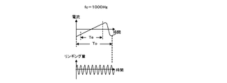
- FIGS. 4A to 4C are explanatory diagrams for explaining the relationship between the driving waveform for driving the optical scanner 10 and the ringing of the reflection unit 6.
- FIG. in the present embodiment the suppression frequency fc of the component of the specific frequency fc (hereinafter referred to as the suppression frequency fc) that is suppressed in advance in order to make the ringing amount smaller than a predetermined value in the drive waveform that drives the reflection unit 6.
- the suppression frequency fc the suppression frequency of the component of the specific frequency fc
- FIG. 4A shows a case where the specific suppression frequency fc corresponding to the waveform information is 1000 Hz.
- the upper graph in FIG. 4A represents a drive waveform applied to the coil 15 of the reflector 6, the vertical axis represents the current applied to the coil 15, and the horizontal axis represents time.
- the lower graph in FIG. 4A exaggerates the vibration accompanying the ringing of the reflecting portion 6, the vertical axis is the displacement amount of the ringing, that is, the ringing amount, and the horizontal axis is the time.
- the waveform information stored in the waveform information storage unit 3 is read, a waveform is generated by the waveform forming unit 23, and the drive unit 2 outputs the waveform based on the generated waveform.
- 1000 Hz is set as the suppression frequency fc for suppressing the ringing amount. That is, the drive waveform generated from this waveform information means that the component of the suppression frequency fc of 1000 Hz is removed or reduced.
- the drive waveform has a sawtooth shape with a period To, and the frequency is set to 60 Hz, for example.
- the drive waveform increases almost monotonically from the negative maximum current to the positive maximum current, and then rapidly changes to the negative maximum current. Then, it returns to the initial state.
- the component of the suppression frequency fc is removed or reduced, so that the waveform change point has a slightly smooth shape.
- the effective scanning period Te is set while monotonously increasing from the negative maximum current to the positive maximum current.
- the amount of ringing is represented by the magnitude of the swing angle (peak to peak) of the reflector 6. As shown in the lower part of FIG. 4A, when the suppression frequency fc is 1000 Hz as the waveform information, the amount of ringing with respect to the deflection angle of the reflection unit 6 is 1%. This is a state where the resonance frequency of the ringing of the reflecting portion 6 is shifted from the suppression frequency fc for suppressing the ringing.
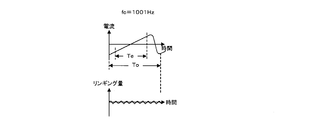
- the waveform information read from the waveform information storage unit 3 is changed, and the suppression frequency fc for suppressing the ringing amount included in the drive waveform is set to 1001 Hz.
- the drive waveform shown in the upper part of FIG. 4B is almost the same as FIG. 4A, but the suppression frequency fc that is removed or reduced from the drive waveform is shifted to the high frequency side by 1 Hz.
- the ringing amount of the reflecting portion 6 is 0.1% with respect to the deflection angle of the reflecting portion 6. This represents a state in which the resonance frequency that causes ringing of the reflecting portion 6 matches the suppression frequency fc for suppressing the ringing, and the ringing is effectively suppressed.
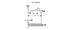
- the waveform information read from the waveform information storage unit 3 is changed, and the suppression frequency fc for suppressing the ringing amount included in the drive waveform is set to 1002 Hz.
- the drive waveform shown in the upper part of FIG. 4C is almost the same as that of FIG. 4A, but the suppression frequency fc removed or reduced from the drive waveform is shifted to the high frequency side by 2 Hz.
- the ringing amount of the reflection unit 6 is 1% with respect to the deflection angle of the reflection unit 6. This is a result of deviation between the resonance frequency of the ringing of the reflector 6 and the suppression frequency fc for suppressing the ringing.
- the waveform information storage unit 3 stores one cycle To of the drive waveform shown in FIGS. 4A to 4C. For example, the current value for each timing is stored. In this case, for example, a plurality of drive waveforms in which the suppression frequency fc for suppressing the ringing amount is changed by 1 Hz are stored as waveform information.
- the waveform information setting unit 22 specifies waveform information, reads specific waveform information for one period To from the waveform information storage unit 3 and transmits it to the waveform forming unit 23, and the waveform forming unit 23 converts the continuous waveform data into a DA converter. 24. 4A to 4C, the suppression frequency fc is 1000 Hz to 1002 Hz, but the present invention is not limited to this.
- the suppression frequency fc can be any frequency that reduces the ringing amount, and the amount of change to be changed may be 1 Hz or a frequency higher than this.
- the waveform information storage unit 3 may store a plurality of suppression frequencies fc for suppressing the ringing amount as parameter values instead of storing one cycle To of the drive waveform.
- the waveform information setting unit 22 specifies a parameter value as waveform information, reads the specific parameter value from the waveform information storage unit 3 and gives it to the waveform forming unit 23, and the waveform forming unit 23 generates waveform data from this parameter value.
- the data may be transmitted to the DA converter 24. Further, it is stored in the waveform information storage unit 3 in association with the suppression frequency fc and physical quantity for suppressing the ringing amount, for example, the temperature change in the environment, the accumulated operation time of the optical scanner 10, the outer shape of the reflection unit 6, and the like.
- the drive waveform may be generated by setting a physical quantity.
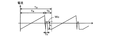
- FIG. 5 shows another example of a driving waveform for driving the optical scanner 10, which is a modification of FIG.
- This modification is an example in which a correction waveform Wc is formed during a drive waveform recovery period, a plurality of drive waveforms obtained by changing the correction waveform Wc are prepared, and ringing is suppressed by sequentially switching.
- the vertical axis represents the current applied to the coil 15 of the reflector 6 and the horizontal axis represents time.
- the current increases approximately monotonically from the negative maximum value to the positive maximum value.
- the current quickly reverses to a negative maximum value, and a correction waveform Wc having a half-cycle shape of a sine wave is given based on the negative maximum value, and then the negative maximum value. Constant current is given.
- the correction waveform Wc is a waveform during a half-cycle period Tx.
- the scanning period Ta and the return period Tb are one period To.
- the drive unit 2 repeatedly applies this drive waveform to the optical scanner 10.
- the waveform information storage unit 3 stores a current value at each timing of one cycle To of the drive waveform shown in FIG.
- the waveform information storage unit 3 stores, for example, a plurality of drive waveforms in which the frequency 1 / (2Tx) of the correction waveform Wc is changed as the suppression frequency fc and the suppression frequency fc is changed little by little as waveform information.
- a plurality of drive waveforms obtained by changing the amplitude h of the correction waveform Wc little by little are stored as waveform information.
- the waveform information setting unit 22 sequentially reads the stored waveform information and gives it to the waveform forming unit 23, and the waveform forming unit 23 outputs continuous waveform data corresponding to each waveform information to the DA converter 24.
- a driving waveform in which the correction waveform Wc changes little by little is sequentially given to the reflection unit 6, and the driving waveform setting unit 4 has a waveform in which the ringing amount becomes smaller than a predetermined value from the ringing amount detected by the detection unit 5.
- Information can be selected.
- the special waveform as shown in FIG. 5 may be processed as described with reference to FIG. That is, instead of the normal sawtooth waveform, a special waveform as shown in FIG. 5 is used as the basic drive waveform, and a plurality of drives in which the suppression frequencies fc of the suppressed components other than the correction waveform Wc are different from the basic drive waveform. It may be configured to store and switch waveforms. Further, a configuration may be employed in which a plurality of waveforms (for example, the waveforms in FIG. 5) that are effective or effective for ringing in various states are stored and switched without considering elements such as the suppression frequency fc.
- FIG. 6 is an explanatory diagram for explaining the operation of the optical scanning device 1 according to the embodiment of the present invention.
- the vertical axis of the graph shown in FIG. 6 represents the ringing amount detected by the detection unit 5, and the horizontal axis is a parameter value for specifying the waveform information stored in the waveform information storage unit 3, Corresponds to the frequency.
- the drive waveforms shown in FIGS. 4A to 4C or 5 correspond to the suppression frequency fc.
- the predetermined value yo represents an allowable limit level of the ringing amount. If the detected ringing amount is smaller than the level of the predetermined value yo, for example, when the optical scanner 10 is applied to an image display device, the quality of the projected image is deteriorated due to ringing. Will be negligible.
- the drive waveform setting unit 4 specifies the frequency f1 and reads the waveform information corresponding to the frequency f1 from the waveform information storage unit 3.
- the drive waveform setting unit 4 generates waveform data from the read waveform information.
- the drive unit 2 generates a drive waveform from the waveform data and drives the optical scanner 10.
- the drive waveform setting unit 4 compares the ringing amount y1 detected by the detection unit 5 with the predetermined value yo and determines that y1 is larger than the predetermined value yo.
- the drive waveform setting unit 4 reads waveform information corresponding to the frequency f2 from the waveform information storage unit 3 to generate waveform data, and the drive unit 2 generates a drive waveform from this waveform data and drives the optical scanner 10. .
- the drive waveform setting unit 4 compares the ringing amount y2 detected by the detection unit 5 with the predetermined value yo and determines that the ringing amount y2 is larger than the predetermined value. Thereafter, the drive waveform is sequentially changed to the frequency yn, the detected ringing amount is compared with the predetermined value, and the detection is repeated until the detected ringing amount becomes smaller than the predetermined value yo.
- FIG. 6 shows that the detected ringing amount y3 is smaller than the predetermined value yo when the optical scanner 10 is driven by the drive waveform based on the waveform information corresponding to the frequency f3.
- the drive waveform setting unit 4 sequentially reads waveform information corresponding to frequencies f7, f8, and f9 higher than the frequency f3 from the waveform information storage unit 3 to generate waveform data, and the drive unit 2 is generated by the waveform data.
- the drive waveform setting unit 4 sequentially obtains each ringing amount detected by the detection unit 5.
- the drive waveform setting unit 4 selects waveform information corresponding to the frequency (f8 in FIG. 6) that is the lowest ringing amount from the detected ringing amount.
- the drive waveform setting unit 4 gives the waveform data based on the selected waveform information to the drive unit 2 to set the drive waveform.
- the relationship between the ambient temperature change and the suppression frequency fc may be measured in advance, and the temperature and the suppression frequency fc may be associated and stored in the waveform information storage unit 3.
- waveform information corresponding to the change in the integration time is stored in advance in the waveform information storage unit 3 as the integration time in which the horizontal axis is changed to temperature and the reflection unit 6 is driven, and the integration time is changed in the drive waveform setting process. You may make it make it.
- waveform information when the ambient environment changes over time or the like is stored in advance, the amount of ringing superimposed on the swing of the reflection unit 6 is detected, and the waveform information that decreases the amount of ringing is obtained.
- the ringing amount of the reflecting portion 6 can be driven smaller than a predetermined value.
- FIG. 7A and 7B are explanatory diagrams for explaining the operation of the optical scanning device 1 according to another embodiment of the present invention.
- the vertical axis represents the amount of ringing detected by the detection unit 5
- the horizontal axis represents parameter values for specifying the waveform information stored in the waveform information storage unit 3. It corresponds to a frequency as a physical quantity, for example, a suppression frequency.
- FIG. 7A shows the first drive waveform setting process, in which the frequency is roughly changed.
- FIG. 7B represents the second drive waveform setting process, and the frequency is finely changed.
- the drive waveform setting unit 4 sequentially reads each waveform information corresponding to the frequencies f1, f5, f9, and f13 from the waveform information storage unit 3 and outputs waveform data based on the waveform information to the drive unit. 2 is sequentially applied, and the optical scanner 10 is driven by the drive waveform generated based on the waveform information corresponding to each frequency.
- the drive waveform setting unit 4 compares the ringing amount detected by the detection unit 5 with the predetermined value yo in each drive waveform, and specifies the two frequencies f5 and f9 with the smallest ringing amount.
- the drive waveform setting unit 4 sequentially reads each waveform information corresponding to the frequencies f6, f7, and f8 between the frequency f5 and the frequency f9 from the waveform information storage unit 3, and this waveform information. Are sequentially supplied to the drive unit 2 to drive the optical scanner 10 with the drive waveform generated based on the waveform information corresponding to each frequency.
- the drive waveform setting unit 4 compares the ringing amount detected by the detection unit 5 in each drive waveform with a predetermined value, and selects a frequency at which the ringing amount is at least smaller than the predetermined value and has the lowest ringing amount.
- waveform data based on the waveform information corresponding to the selected frequency (in this case, frequency f7) is given to the drive unit 2 to set a drive waveform.
- the drive waveform is first roughly changed, the parameter value whose ringing amount is smaller than the predetermined value is specified, the drive waveform is further changed finely, and the drive waveform that minimizes the ringing amount is selected.
- the ringing amount of the part 6 can be suppressed quickly and to the minimum.
- the frequency as the parameter value corresponding to the physical quantity
- the amplitude, the ambient temperature change, the integrated drive time of the reflection unit 6 and the like can be used.
- FIG. 8 is an explanatory diagram for explaining the operation of the optical scanning device 1 according to another embodiment of the present invention.
- the vertical axis of the graph shown in FIG. 8 represents the amount of ringing detected by the detection unit 5, and the horizontal axis is a parameter value for specifying the waveform information stored in the waveform information storage unit 3. Corresponds to the frequency.
- the vertical axis in FIG. 8 represents the ringing amount, and the horizontal axis represents the frequency.
- the drive waveform setting unit 4 reads waveform information corresponding to the frequency f1 and the frequency f2 from the waveform information storage unit 3, gives waveform data based on the waveform information to the drive unit 2, and drives based on the read waveform information.
- a waveform is generated to drive the optical scanner 10.
- the waveform information corresponding to the frequency fo is not stored, the waveform information corresponding to the frequency closest to the frequency fo is read from the waveform information storage unit 3.
- the drive waveform setting unit 4 gives the waveform data formed based on the read waveform information to the drive unit 2, generates a drive waveform, and drives the optical scanner 10.
- the drive waveform setting unit 4 confirms that the ringing amount detected by the detection unit 5 is smaller than the predetermined value yo, sets the drive waveform based on the waveform information, and drives the optical scanner 10. As a result, the drive waveform can be set in a short time.
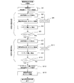
- FIG. 9 shows a driving method of the optical scanning device 1 according to the embodiment of the present invention, and is a flowchart of the drive waveform setting process of the optical scanning device 1.
- This drive waveform setting process is separated into steps S2 to S6 that are the first selection process and steps S7 to S11 that are the second selection process.
- the parameter value fx when the ringing amount y falls below the predetermined value yo is obtained, and in the second selection process, the parameter value f that minimizes the ringing amount y is obtained.
- a drive waveform is generated based on the waveform information W corresponding to the parameter value f that minimizes the ringing amount y. This will be specifically described below.
- the drive waveform selection process of the optical scanning device 1 is set to start automatically when the driving of the optical scanning device 1 is started or when a predetermined condition is satisfied during driving.
- the drive waveform setting unit 4 performs initial setting under the control of the CPU (step S1).
- a predetermined value yo indicating the upper limit of the allowable ringing amount
- a parameter setting for changing the driving waveform of the optical scanner 10 a parameter value change width ⁇ m, ⁇ n ( ⁇ m, ⁇ n are integers), and the like are set.
- the first selection process is as follows.
- the drive waveform setting unit 4 reads the waveform information W (m) corresponding to the parameter value f (m) (m is a positive integer) from the waveform information storage unit 3 (step S2).
- the drive waveform setting unit 4 generates waveform data from the read waveform information W (m) and supplies the waveform data to the drive unit 2.
- the drive unit 2 inputs the waveform data, generates a drive waveform, and drives the optical scanner 10 (step S3).
- the detection unit 5 detects the ringing amount y (m) of the reflection unit 6 by the swing detection element 16 installed in the optical scanner 10 (step S4).
- the change width ⁇ m is set to 1.
- the change width ⁇ m is set to an integer value of 1 or more (step S6).
- step S5 when the drive waveform setting unit 4 determines that the detected ringing amount y (m) is smaller than the predetermined value yo (Yes in step S5), the process proceeds to the second selection process.
- the second selection process is as follows.
- the drive waveform setting unit 4 sets the range f (n min ) to f (n max ) of the parameter value f to be changed and the change width ⁇ m.
- the selection process can be performed in order.
- the parameter value range f (mx) to f (m + x) and the change width ⁇ n are finely changed before and after the parameter value f (m) giving the ringing amount y (m) below the predetermined value yo. Also good.
- the drive waveform setting unit 4 reads waveform information W (n min ) corresponding to the parameter value f (n min ) (step S7).
- the drive waveform setting unit 4 generates waveform data from the read waveform information W (n) and supplies the waveform data to the drive unit 2.
- the drive unit 2 generates a drive waveform based on this waveform data, and drives the optical scanner 10 (step S8).
- the ringing amount y (n min ) of the reflection unit 6 is detected by the detection elements installed in the detection unit 5 and the optical scanner 10 (step S9) and stored in a predetermined storage unit.
- the drive waveform setting unit 4 specifies a parameter value f (n x ) that minimizes the ringing amount out of the ringing amount y (n min ) to the ringing amount y (n max ) stored in the predetermined area. (n x is an integer), to select the parameter value f (n x) in the corresponding waveform information W (n x) (step S12).
- the drive waveform setting unit 4 generates waveform data from the selected waveform information W (n x ) and supplies the waveform data to the drive unit 2.
- the drive unit 2 generates a drive waveform from the waveform data, gives it to the optical scanner 10, drives the optical scanner (step S13), and ends the drive waveform setting process.
- the first selection process and the second selection process are performed.
- the drive waveform is set based on the parameter value f (m) selected in the first selection process. May be. That is, when the drive waveform setting unit 4 detects that the ringing amount y (m) detected in the first selection process is smaller than the predetermined value yo (Yes in step S5), the second selection process is omitted. Then, the waveform information W (m) that minimizes the ringing amount is selected (step S12), and the drive unit 2 sets the drive waveform based on the waveform information and drives the optical scanner 10. Good (step S13).
- the change width ⁇ m in the first selection process is a large value and the change width ⁇ n in the second selection process is a small value. That is, as the parameter value corresponding to the physical quantity, the change width of the first parameter value is made coarse, and the change width of the parameter in the second selection process is made fine. Thereby, it becomes possible to set the drive waveform of the optimum condition quickly.
- the parameter value f is further changed to roughly relate the ringing amount y to the parameter value f. Ask for.
- FIG. 10 is a configuration diagram of the retinal scanning image display apparatus 30 according to the embodiment of the present invention. As shown in FIG. 10, the retinal scanning image display device 30 directly forms an image on the retina 53 of the user's eyeball 52. This will be specifically described below.
- the video signal processing circuit 36 receives the video signal, generates a light source driving signal corresponding to blue (B), green (G), and red (R), and a B laser driving circuit 37 as a light source driver.
- a light source driving signal corresponding to blue (B), green (G), and red (R)
- B blue
- G green
- R red
- the B laser element 40 emits blue light whose light intensity is modulated according to the blue drive signal from the B laser drive circuit 37
- the G laser element 41 has light intensity according to the green drive signal from the G laser drive circuit 38.
- the modulated green light is emitted
- the R laser element 42 emits red whose light intensity is modulated in accordance with the red drive signal from the R laser drive circuit 39.
- each laser element is converted into parallel light by the collimating optical system 43, synthesized by the dichroic mirror 44, condensed by the coupling optical system 45, and incident on the optical fiber 46.
- the image light emitted from the optical fiber 46 is applied to the mirror of the high-speed optical scanner 48 via the second collimating optical system 47.
- the mirror section of the high-speed optical scanner 48 is driven and oscillated by the horizontal scanning drive circuit 34 to scan the reflected light in the main scanning direction.
- the image light scanned in the main scanning direction is irradiated to the low-speed optical scanner 10 which is the optical scanning device according to the present invention via the first relay optical system 49.
- the low-speed optical scanner 10 scans reflected light in the sub-scanning direction with the mirror surface oscillating by a magnetic field.
- the image light reflected from the reflection unit 6 of the low-speed optical scanner 10 forms an image on the retina 53 of the eyeball 52 via the second relay optical system 51.
- the beam detector (BD) 50 detects the light scanned from the high-speed optical scanner 48 and outputs it to the BD signal detection circuit 35.
- the video signal processing circuit 36 receives the BD signal from the BD signal detection circuit 35 and generates a reference timing.
- the video signal processing circuit 36 outputs a synchronization signal synchronized with the light source driving signal to each of the horizontal scanning driving circuit 34 and the vertical scanning control unit 31.
- the high-speed optical scanner 48 receives a horizontal drive waveform from the horizontal scanning drive circuit 34 and swings its mirror portion at high speed based on resonance vibration.
- the vertical scanning control unit 31 includes a drive waveform setting unit 4 and a waveform information storage unit 3.
- the vertical scanning control unit 31 actually reads a CPU (not shown) for controlling the operation of the vertical scanning control unit 31, a ROM (not shown) for storing a control program, and temporarily stores the control program.
- the drive waveform setting unit 4 is realized by a RAM (not shown) used as a work area and the CPU executing a control program.
- the drive waveform setting unit 4 executes drive waveform selection processing when the retinal scanning image display device 30 is activated or at a predetermined timing, and specifies waveform data for driving the low-speed optical scanner 10.
- the drive unit 2 inputs the identified waveform data, generates a drive waveform, and drives the low-speed optical scanner 10.
- the drive waveform is synchronized with the light source drive signal input from the video signal processing circuit 36.
- the detection unit 5 detects a ringing amount superimposed on the oscillation from an oscillation detection element (not shown) installed in the reflection unit 6 of the low-speed optical scanner 10.
- the drive waveform setting unit 4 selects waveform information in which the detected ringing amount is equal to or less than a predetermined value yo, and sets the drive waveform. The details of the drive waveform selection process have already been described, and are omitted here.
- the ringing amount is set to a predetermined value even when the ringing superimposed on the oscillation of the low-speed optical scanner 10 is affected over time or due to environmental changes. Since the drive waveform is automatically set so as to be less than or equal to the value, it is possible to prevent the quality of the projected image from being deteriorated over time and to always display a stable image.
- the retinal scanning image display device has been described.
- the second relay optical system 51 is replaced with a projection optical system, and a screen that displays a projection image instead of the retina 53, a projection-type image display device is used.
- An image display device can be made.
Landscapes
- Physics & Mathematics (AREA)
- General Physics & Mathematics (AREA)
- Optics & Photonics (AREA)
- Electromagnetism (AREA)
- Mechanical Optical Scanning Systems (AREA)
- Mounting And Adjusting Of Optical Elements (AREA)
- Facsimile Scanning Arrangements (AREA)
Abstract
光走査装置の揺動に重畳されるリンギングが、経時的に或いは環境変化により増大し、走査光にむらが生じて描画される画像の品質が低下することを防止する。
光ビームを揺動する反射部により走査する光走査装置1であり、反射部6を揺動させる駆動波形を生成する駆動部2と、駆動波形の生成に使用される波形情報を複数記憶する波形情報記憶部3と、複数の波形情報から一つの波形情報を選定し、選定された波形情報を駆動部に与えて駆動波形を設定する駆動波形設定部4と、反射部6の揺動に重畳されるリンギング量を検出する検出部5とを備え、駆動波形設定部4は、波形情報記憶部3に記憶された複数の波形情報を駆動部2に順次与え、検出部5により検出されたリンギング量が所定値よりも小さくなる波形情報を選定する。
Description
本発明は、光ビームを走査するために用いられる光走査装置に関する。特に、光ビームを二次元的に走査して投影画像を形成する画像表示装置に適用できる。
光走査装置は、コピー機や印刷機の光スキャナとして、あるいは投影装置の光スキャナとして使用されている。図11Aはこの種の光走査装置100が光走査を行う様子を表す模式図である。反射部101の表面には反射面が形成されている。反射部101の反射面に光源103から光ビームを照射する。反射部101の反射面が形成されていない裏面には、例えば図示しないコイルが形成されおり、反射部101の周囲には磁石が設置されている。このコイルに交番電流からなる駆動信号を与えることにより、フレミングの左手の法則により、電流路にローレンツ力が加えられて、揺動軸を中心に反射部が揺動する。この反射部の揺動により反射面に入射した光ビームは反射される際に走査光として走査される。光源103は、駆動回路102から例えば画像信号に応じて強度変調された駆動信号が与えられ、点灯と消灯とを繰り返す。反射部101の揺動と光源103の点灯及び消灯とを同期させて駆動することにより、反射部101により反射される走査光により描画することができる。
図11Bは反射部101を駆動する駆動信号の一例を表し、2次元走査により画像を投影する場合の垂直走査を表している。横軸が時間を表し縦軸は電流の振幅を表している。駆動信号は、時間に対して振幅が鋸波形状の周期的形状を有している。図11Cは、反射部101の揺動状態を表している。横軸が時間であり縦軸が反射面のミラー角度を表している。ミラー角度は反射部に駆動信号を与えない水平状態を基準として鋸波状に周期的に揺動する。
しかし、ミラー角度は矢印により示す挿入図に示されるように、微小振動からなるリンギングが重畳される。このリンギングが重畳されると、走査光もこの微小振動の周期が重畳され、走査速度にむらが重畳されることになる。この光走査装置を用いて画像表示を行うと、表示される画像の走査線にも粗密のむらが現れ、画像品質を劣化させることになる。
図11Cの挿入図に示されるリンギングは次のような原因で発生する。図11Aに示す光走査装置100は、反射部101が支持部により支持されている。反射部101が回転すると、これを支持する支持部のねじれ弾性により回転を復元する復元力が働く。そのため、反射部101の慣性モーメントと支持部のねじれ弾性により定まる固有振動を有することになる。また、図11Aに示すような構造でなくとも、反射部101の回転に機械的、電気的又は磁気的に回転を復元する復元力が与えられる場合には、固有振動を生ずることになる。
一方、図11Bに示すように、光走査装置を2次元画像表示の垂直走査として使用する場合は、画像を表示する走査期間において駆動信号は直線的に増加し、画像を表示しない復帰期間に移行したとき又は復帰期間から走査期間に移行したときに駆動信号は急激に変化する。即ち、駆動信号は鋸波形状の頂点付近で急激に変化する。この駆動信号の急激な変化は反射部101に衝撃を与えることになり、反射部101には固有の共振振動が誘起される。一旦、反射部101に共振振動が生ずると、これを打ち消すような駆動信号を与えない限りしばらく持続する。例えば、画像表示装置の垂直走査に光走査装置を適用した場合に、共振振動は1フレーム期間以上持続し、投影画像の品質を低下させる原因となる。
特許文献1には、ガルバノ・ミラーに鋸波形状の駆動電流を与えたときに発生するこの種のリンギングを、駆動電流の復帰期間に段階状のパルスを与えて低減することが記載されている。そして段階状のパルス幅やパルス高を適切に選択することにより、リンギングの抑制することができることが記載されている。特許文献2には、ガルバノ型スキャナを駆動するシステムにおいて、ガルバノ型スキャナを駆動するための駆動パターンをROM内に複数記憶しておき、予め設定しておいた駆動パターンに対して実際の使用時にずれが生じたときでも、駆動パターンを選択することによりそのずれに対応することができ、外部に高価な指令発生器を接続する必要がないことが記載されている。
特開昭54-89673号公報
特開2005-338450号公報
しかしながら、この種の光走査装置は、製造時に特性を均一化するのは難しく、特性のばらつきが生じたりしたため、リンギングを低減するのが容易でなかった。また、周囲の環境変化、光走査装置の経時的な変化、例えば反射部を支持する支持部のねじれ弾性率の変化等により、リンギングの共振周波数や振幅が経時的に変化する。そのために、リンギングを初期設定では抑制したつもりでも、使用を続けると増加してくる。また、温度変化等の環境が変化した場合にも、同様にリンギングが増加する場合があった。
そこで、本発明は、反射部の初期特性がばらついたり、揺動特性が経時的に変化したりして、不要なリンギングが誘起されたり、増加する場合でも、複数ある駆動波形のうち何れかを選定することにより、リンギング量を所定値以下に制御可能な光走査装置、画像表示装置及び光走査装置の駆動方法を提供することを目的とする。
上記目的を達成するために、本発明の一つの観点によれば、光走査装置において、揺動により光ビームを走査する反射部と、前記反射部を揺動させるための駆動波形を生成する駆動部と、前記駆動波形の生成に使用される波形情報を複数記憶する波形情報記憶部と、前記複数の波形情報から一つの波形情報を選定し、前記選定された波形情報に基づいて駆動波形を設定する駆動波形設定部と、前記反射部の揺動に含まれる不要な振動に基づくリンギング量を検出する検出部と、を備え、前記駆動波形設定部は、前記波形情報記憶部に記憶された複数の波形情報を前記駆動部に順次与えて、前記検出されたリンギング量が所定値よりも小さくなる波形情報を選定することとした。
このように構成することにより、経時的に変化する場合の波形情報を予め記憶しておき、反射部の揺動に重畳されるリンギング量を検出し、そのリンギング量が低下する波形情報を選定して、反射部のリンギング量を所定値よりも小さく駆動することができる。
また、前記光走査装置においては、前記駆動波形は鋸波状又は三角波状の周期的形状を有し、前記検出部は、前記反射部の有効走査期間のリンギング量を検出する構成にしてもよい。
このように構成することにより、鋸波形状又は三角波形状の駆動波形により反射部を駆動する際に、駆動波形の急激な変化により生ずるオーバーシュート等の影響を受けることなく実質的なリンギング量を検出することができる。
また、前記光走査装置においては、前記検出部は、前記反射部の揺動を検出するための圧電素子を含む構成にしてもよい。
このように構成することにより、反射部の揺動の振幅や周期を簡便に検出することができる。
また、前記光走査装置においては、前記波形情報は、特定の周波数の成分が抑圧されたような周波数成分を含み、前記波形情報記憶部は、前記特定の周波数が異なる複数の波形情報を記憶し、前記駆動波形設定部は、前記特定の周波数が異なる波形情報を前記駆動部に順次与える構成にしてもよい。
このように構成することにより、反射部の固有振動に伴うリンギングを効果的に低減させることができる。
また、前記光走査装置においては、前記波形情報は、前記反射部の前記振動に影響を与える物理量に対応するパラメータ値を含み、前記駆動波形設定部は、前記物理量が粗く変化する複数のパラメータ値を設定し、前記設定された複数のパラメータ値に対応する複数の波形情報を前記駆動部に順次与え、前記検出されたリンギング量が前記所定値よりも小さくなるパラメータ値を特定し、前記特定されたパラメータ値に基づいて、前記物理量が細かく変化するパラメータ値を設定し、前記設定されたパラメータ値に対応する波形情報を前記駆動部に与え、前記検出されたリンギング量が最小となる波形情報を選定する構成にしてもよい。
このように構成することにより、まず粗く駆動波形を変化させ、リンギング量が所定値より小さくなるパラメータ値を特定して、更に細かく駆動波形を変化させて、リンギング量が最小となる駆動波形を選定するので、反射部のリンギング量を迅速にかつ最小に抑制することができる。
また、前記光走査装置においては、前記駆動波形設定部は、前記物理量が細かく変化する複数のパラメータ値を設定し、前記設定された複数のパラメータ値に対応する複数の波形情報を前記駆動部に順次与える構成にしてもよい。
前記光走査装置からなる低速光走査装置と、高速光走査装置と、画像信号に基づいて強度変調された光ビームを生成して前記光走査装置に照射する光源と、前記光走査装置から走査された光ビームを投射する投影レンズ系を含む画像表示装置とした。
このように構成することにより、経時的に変化した場合の波形情報を予め記憶しておき、反射部の揺動に重畳されるリンギング量を検出して予め記憶しておいた波形情報を選定し、反射部のリンギング量を所定値よりも小さくすることができるので、投影される画像の品質が経時的に低下することを防止することができる。
前記反射部を揺動させるための駆動波形を生成する駆動部と、前記駆動波形の生成に使用される波形情報を複数記憶する波形情報記憶部と、前記複数の波形情報から一つの波形情報を選定し、前記選定された波形情報を前記駆動部に与えて駆動波形を設定する駆動波形設定部と、前記反射部の揺動に重畳される振動に基づくリンギング量を検出する検出部と、を備える光走査装置の駆動方法において、前記駆動波形設定部は、前記波形情報記憶部に記憶された複数の波形情報を読み出すステップと、前記読み出した波形情報を前記駆動部に与えて前記反射部を揺動させるステップと、前記検出部により検出されたリンギング量と、所定値とを比較し、検出されたリンギング量が前記所定値よりも小さくなったときの波形情報を選定するステップと、前記選定された波形情報を前記駆動部に設定して前記反射部を駆動するステップと、を備える光走査装置の駆動方法とした。
かかる方法とすることにより、反射部を揺動させるための駆動波形を生成する駆動部と、駆動波形の生成に使用される波形情報を複数記憶する波形情報記憶部と、複数の波形情報から一つの波形情報を選定し、選定された波形情報に基づいて駆動波形を設定する駆動波形設定部と、反射部の揺動に含まれる不要な振動に基づくリンギング量を検出する検出部とを備え、駆動波形設定部は、波形情報記憶部に記憶された複数の波形情報を駆動部に順次与えて、検出されたリンギング量が所定値よりも小さくなる波形情報を選定するようにした。これにより、経時的に変化する場合の波形情報を予め記憶しておき、反射部の揺動に重畳されるリンギング量を検出し、そのリンギング量が低下する波形情報を選定して、反射部のリンギング量を所定値よりも小さく駆動することができる。
1 光走査装置
2 駆動部
3 波形情報記憶部
4 駆動波形設定部
5 検出部
6 反射部
7 入射ビーム
8 走査ビーム
9 揺動軸
10 光スキャナ
11 枠
12 支持部
13 磁石
14 圧電素子
15 コイル
16 揺動検出素子
30 網膜走査型画像表示装置
2 駆動部
3 波形情報記憶部
4 駆動波形設定部
5 検出部
6 反射部
7 入射ビーム
8 走査ビーム
9 揺動軸
10 光スキャナ
11 枠
12 支持部
13 磁石
14 圧電素子
15 コイル
16 揺動検出素子
30 網膜走査型画像表示装置
以下、本発明の一実施形態について、図面を用いて詳細に説明する。
図1は、本発明に係る光走査装置1の基本的な構成図を表わす。図1において、光走査装置1は、入射光ビーム7を走査光ビーム8に変換する反射部6と、この反射部6を駆動する駆動部2と、反射部6の揺動を検出する検出部5と、複数の波形情報を記憶する波形情報記憶部3と、波形情報記憶部3から波形情報を読み出して駆動部2に順次与え、検出部5によりリンギング量を検出し、この検出されたリンギング量が所定値より小さくなる波形情報を選定し、この選定された波形情報に基づいて駆動波形を設定する駆動波形設定部4とから構成されている。なお、ここでリンギング量とは、光スキャナ10により走査される1走査期間のうち、有効な走査期間である有効走査期間のうちのある範囲におけるリンギングの平均振幅又はピークtoピーク値をいう。
反射部6は、後に詳細に説明する光スキャナ10の揺動部である。反射部6の表面には反射面が形成されている。反射部6は、揺動軸9に与えるねじれ回転や、反射部6に直接与える静電気的又は電磁気的又はピエゾ効果による力により揺動を誘起させることができる。例えば、ピエゾ素子により揺動軸9にねじれ回転を与えて、反射部6を揺動させることができる。また、反射部6の反射面とは反対側の裏面にコイルを形成し、反射部6に外部磁界に与えるとともに、コイルに交番電流を流す、あるいは外部磁界を交番させて、ローレンツ力により揺動を誘起させることもできる。また、反射部6の裏面に裏面電極を形成し、反射部6の外部にこの裏面電極に近接して外部電極を形成し、いずれか又は両方の電極に交番電圧を印加して反射部6を揺動させることができる。
駆動部2は、駆動波形設定部4により与えられる波形データに基づいて反射部6を揺動させるための駆動波形を生成する。駆動部2をDAコンバータと増幅器により構成し、駆動波形設定部4から電圧値の時系列データからなる波形データを入力して駆動波形を生成することができる。また、駆動部2をパラメータ値の設定により駆動波形を生成する駆動波形発生部と増幅器により構成し、波形データとしてパラメータ値を入力するようにしてもよい。駆動波形は、光走査装置1の用途により異なるが、例えば光走査装置1を、2次元画像を形成するための垂直走査の光スキャナとして使用する場合には、駆動波形は鋸波状又は三角波状の周期的形状を有している。反射部6の反射面を一定の角速度で揺動させるためである。しかし、駆動波形はこれに限定されず、サイン波の形状であってもよいし他の形状でもよい。
検出部5は、反射部6の揺動軸9に又は揺動軸9を保持する梁部等に設置した圧電素子と、この圧電素子からの出力電圧を増幅する増幅回路により構成することができる。圧電素子は、応力変化を電圧変化に変換するので、反射部6の実際の揺動を検出することができる。また、反射部6の揺動を、加速度センサを利用して検出することができる。例えば、反射部6の裏面に加速センサを構成する。反射部6が一定角速度で揺動する場合は加速度センサの検出感度は低下するが、反射部6において微小振動によるリンギングが発生している場合は、加速度センサに加速度を加わる。従って、加速度センサは、一定角速度の揺動を除去するフィルタ機能も兼ね備えたリンギング量検出手段として利用することができる。また、反射部6の実際の揺動を、反射部6から反射した走査ビームが照射される位置に設置したフォトセンサにより検出することができる。走査ビームが照射される位置に複数のフォトセンサを設置して、リンギング量を検出することができる。
波形情報記憶部3は、駆動波形を生成するための波形情報を複数記憶する。例えば、波形情報記憶部3は、特定の周波数成分が抑圧されたような周波数成分を含み、その特定の周波数がそれぞれ異なる複数の波形情報を記憶している。例えば、反射部6の共振周波数が製造時においてばらついたり、経時的に変化する場合に、この共振周波数の変化を予め複数測定または想定しておき、この測定または想定された複数の共振周波数の夫々に対応する複数の波形情報を波形情報記憶部3に記憶しておく。例えば、波形情報を、反射部6に与える駆動波形の各タイミングにおける1周期分の出力電流値又は出力電圧値から構成し、リンギングの周波数やリンギング量に対応付けて複数記憶する。また、波形情報を、物理量に対応するパラメータ値から構成し、各パラメータ値に基づいて駆動波形が生成されるように構成することができる。パラメータ値として、例えばリンギングの周波数、リンギングの振幅、周囲の温度、反射部6を駆動した積算時間等とすることができる。
駆動波形設定部4は、リンギング量が所定値よりも小さくなる波形情報を選定する選定処理を行い、選定された波形情報により駆動部2から反射部6に与える駆動波形を設定する設定処理を行う。選定処理は次のように行う。駆動波形設定部4は、波形情報記憶部3から波形情報を読み出してこれに基づく波形データを駆動部2に与える。駆動部2は与えられた波形データに基づいて駆動波形を生成する。光スキャナ10は生成された駆動波形により揺動する。検出部5は、反射部6のリンギング量を検出する。駆動波形設定部4は、検出されたリンギング量と所定値とを比較して、検出されたリンギング量が所定値よりも大きいときは、波形情報記憶部3から先の波形情報と異なる波形情報を読み出して、この波形情報に基づいて生成された駆動波形を光スキャナ10に与えて駆動し、上記と同じ処理を繰り返す。駆動波形設定部4が、検出されたリンギング量が所定値よりも小さいことを判定したときに、当該波形情報を選定する。駆動波形設定部4は、この波形情報に基づいて以降光スキャナ10を駆動する設定処理を行う。
例えば、波形情報記憶部3に記憶する波形情報として、反射部6の固有共振周波数foでの固有共振を制限するための波形情報W0と、固有共振周波数fo+δ(δは周波数を表す)を制限するための波形情報W1と、以下同様に固有共振周波数fo+2δに対する波形情報W2、・・・固有共振周波数fo+nδ(nは正又は負の整数)に対する波形情報Wnとを用意しておく。駆動波形設定部4は、波形情報記憶部3から波形情報W0を読み出して波形データを生成し、駆動部2に与える。駆動部2はこの波形データに基づいて駆動波形を生成し、光スキャナ10を駆動する。駆動波形設定部4は、検出部5により検出されたリンギング量と所定値とを比較する。次に、駆動波形設定部4は、波形情報記憶部3から波形情報W1を読み出して、上記と同様に検出されたリンギング量を所定値とを比較し、以降順次これを繰り返す。そして、駆動波形設定部4は、検出したリンギング量が所定値よりも小さくなったときの波形情報を選定し、以後光スキャナ10をこの波形情報に基づいて生成した駆動波形により駆動する。
この場合に、固有共振周波数foが経時的に変化する量をδとして予測しておき、これに対応する波形情報を記憶しておけばよい。例えば、経時的に固有共振周波数がわずかにシフトする場合はδの値は小さくなり、これに対応する波形情報に基づく駆動波形もわずかの変化となる。また、固有共振周波数foが製造時においてばらつく場合に、そのばらつきの範囲が±nδに入るように2n+1個以上の波形情報を記憶しておけばよい。また、固有共振周波数が変化する場合の他に、リンギング量の大きさに応じた波形情報を記憶してもよいし、温度変化や反射部6の駆動積算時間に応じた波形情報を記憶しておくことができる。また、波形情報として、反射部6のリンギングに影響を与える物理量に対応するパラメータ値とする、或いは物理量に対応するパラメータ値を含む波形情報とすることができる。
以下の、本発明について実施の形態に基づいて具体的に説明する。
図2は、本発明の実施形態に係る光走査装置1の構成図である。光スキャナ10を駆動する駆動部2は、駆動波形設定部4から波形データを入力してアナログ波形に変換するDAコンバータ24と、DAコンバータ24からのアナログ波形を増幅し、駆動波形を生成するアンプ25から構成されている。この駆動波形を光スキャナ10に出力して光スキャナ10の反射部6を揺動させる。
検出部5は、光スキャナ10の揺動を検出する揺動検出素子16と、揺動検出素子16からの出力信号を増幅するアンプ17と、アンプ17の出力信号の、例えば低周波成分を除去するためのフィルタ18と、フィルタ18からの出力信号をデジタル信号に変換するADコンバータ19と、ADコンバータ19の出力データからリンギング量を算出すリンギング量算出部20から構成されている。リンギング量算出部20はリンギング量の他にリンギングの周波数を算出することができる。揺動検出素子16は、光スキャナ10の反射部6を支持する支持部に設置した圧電素子である。
駆動波形設定部4は、検出部5から入力するリンギング量と、所定値とを比較する比較部21と、比較部21の比較結果に基づいて波形情報記憶部3から波形情報を読み出し、波形情報を選定又は設定する波形情報設定部22と、設定された波形情報から駆動用の波形データを生成する波形形成部23とから構成されている。波形形成部23は、波形情報記憶部3から読み出した波形情報が、例えば1周期分の波形データから構成される場合に、1周期分の波形データを接続して連続的な波形データを生成する。あるいは、読み出した波形情報がパラメータ値である場合に、このパラメータ値から特定される波形データを生成する。
なお、リンギング量算出部20、比較部21、波形情報設定部22、波形形成部23は、ソフトウエアを実行することにより実現される。図2の光走査装置1は図示しない制御部を備えており、制御部はCPU、ROM、RAMを含んでいる。CPUは、ROMに記憶されたプログラムをRAMに読み出して実行することにより、上記リンギング量算出部20、比較部21、波形情報設定部22、波形形成部23を実現する。また、ADコンバータ19及びリンギング量算出部20、或いは比較部21をソフトウエアを実行して実現することに代えて、リンギング量検出回路や比較回路により構成することができる。
図3A及び図3Bは、本発明の実施形態に係る光走査装置1に使用する光スキャナ10の説明図である。図3Aは光スキャナ10の模式的な斜視図であり、図3Bは光スキャナ10の模式的な背面図である。反射部6は四角形状を有し、その表面に反射面が形成されている。反射部6は2辺に連結する支持部12により支持され、支持部12は枠11に連結して支持されている。つまり、反射部6は2つの支持部12を介して枠11に揺動可能に支持されている。
反射部6の揺動軸9に平行な2辺に近接して永久磁石13が設置されている。永久磁石13の磁界は、静止状態の反射部6の反射面に平行し、揺動軸9に直行する方向である。反射部6の反射面と反対側の裏面にはコイル15が形成されている。コイル15の電極は2つの支持部12を介して外部に接続する。この構成により、コイル15に電流を流すとコイル15にローレンツ力が働く。揺動軸9から下半分のコイル15には例えば紙面上方にローレンツ力が働き、揺動軸9から上半分のコイルには紙面の裏面側にローレンツ力が働く。これにより、反射部6には揺動軸9を中心として回転トルクが生ずる。従って、電流の大きさを制御することにより、反射部6の揺動角を制御することができる。
支持部12には反射部6の揺動を検出するための圧電素子14が設置されている。反射部6が揺動して支持部12にネジレが生じ、圧電素子14に応力が加わる。圧電素子14は、加えられた応力に応じて電圧を発生するので、この電圧変化を検出することにより、反射部6の揺動の振幅や周期を簡便に検出することができる。
図4A~図4Cは、上記光スキャナ10を駆動するための駆動波形と反射部6のリンギングとの関係を説明するための説明図である。本実施形態では、反射部6を駆動する駆動波形において、予めリンギング量を所定値より小さくするために抑圧される特定の周波数fc(以降、抑圧周波数fcとする)の成分のその抑圧周波数fcを変化させて、反射部6のリンギングを低減させる。
図4Aは、波形情報に対応する特定の抑圧周波数fcを1000Hzとした場合である。図4Aの上段のグラフは、反射部6のコイル15に与える駆動波形を表し、縦軸がコイル15に与える電流であり、横軸が時間である。図4Aの下段のグラフは、反射部6のリンギングに伴う振動を誇張して表しており、縦軸がリンギングの変位量、即ちリンギング量であり、横軸が時間である。
反射部6に与える駆動波形は、波形情報記憶部3に記憶された波形情報が読み出され、波形形成部23により波形が生成され、この生成された波形に基づいて駆動部2により出力される。波形情報には、リンギング量を抑圧するための抑圧周波数fcとして1000Hzが設定されている。つまり、この波形情報から生成される駆動波形は1000Hzの抑圧周波数fcの成分が除かれているか、或いは、低減されていることを意味する。
図4Aの上段のグラフに示すように、駆動波形は周期Toの鋸波状の形状を有し、周波数は例えば60Hzに設定されている。駆動波形は、負の最大電流から正の最大電流に概ね単調に増加した後、負の最大電流へ急激に変化する。その後、最初の状態に戻る。この駆動波形は、上記抑圧周波数fcの成分が除かれているか又は低減しているので、波形の変化点が若干滑らかな形状となる。また、負の最大電流から正の最大電流に単調増加する間に有効走査期間Teが設定されている。光走査装置1を画像表示装置における垂直走査装置として使用する場合は、有効走査期間Teにおいて投影像を投影する。従って、この有効走査期間Teにおいてリンギング量を低減すれば、投影画像の品質低下を防止することができる。
リンギング量は反射部6の揺動角の大きさ(ピークtoピーク)により表している。図4Aの下段に示すように、波形情報として抑圧周波数fcを1000Hzとした場合には、反射部6の振れ角に対するリンギング量は1%である。これは、反射部6のリンギングの共振周波数と、リンギングを抑圧する抑圧周波数fcとがずれている状態である。
図4Bは、波形情報記憶部3から読み出す波形情報を変更して、駆動波形に含まれるリンギング量を抑圧するための抑圧周波数fcを1001Hzに設定している。図4Bの上段に示す駆動波形は、見かけ上図4Aとほとんど変わらないが、駆動波形から除かれる又は低減される抑圧周波数fcが1Hz分高周波側にシフトしている。一方、図4Bの下段に示すように、反射部6のリンギング量は反射部6の振れ角に対するリンギング量は0.1%である。これは、反射部6のリンギングを発生させる共振周波数と、リンギングを抑圧するための抑圧周波数fcとが一致し、リンギングが効果的に抑制された状態を表している。
図4Cは、波形情報記憶部3から読み出す波形情報を変更して、駆動波形に含まれるリンギング量を抑圧するための抑圧周波数fcを1002Hzに設定している。図4Cの上段に示す駆動波形は、見かけ上図4Aとほとんど変わらないが、駆動波形から除かれる又は低減される抑圧周波数fcが2Hz分高周波側にシフトしている。一方、図4Cの下段に示すように、反射部6のリンギング量は反射部6の振れ角に対するリンギング量は1%である。これは、反射部6のリンギングの共振周波数とリンギングを抑圧するための抑圧周波数fcとがずれた結果である。
波形情報記憶部3は、図4A~図4Cに示す駆動波形の1周期To分を記憶しておく。例えば、各タイミングに対する電流値を記憶しておく。この場合に、例えば、リンギング量を抑圧するための抑圧周波数fcを1Hzずつ変化させた駆動波形を波形情報として複数記憶しておく。波形情報設定部22は波形情報を特定し、波形情報記憶部3から1周期To分の特定の波形情報を読み出して波形形成部23に送信し、波形形成部23は連続した波形データをDAコンバータ24に送信する。なお、図4A~図4Cにおいては抑圧周波数fcを1000Hzから1002Hzとしているが、これに限定されない。抑圧周波数fcは、リンギング量を低減させる任意の周波数とすることができ、変化させる変化量として1Hzでもよいしこれ以上の周波数であってもよい。
また、波形情報記憶部3は、駆動波形の1周期Toを記憶することに変えて、リンギング量を抑圧するための抑圧周波数fcをパラメータ値として複数記憶しておくようにしてもよい。波形情報設定部22は波形情報としてのパラメータ値を特定し、波形情報記憶部3から特定のパラメータ値を読み出して波形形成部23に与え、波形形成部23はこのパラメータ値から波形データを生成し、DAコンバータ24に送信するようにしてもよい。また、リンギング量を抑圧するための抑圧周波数fcと物理量、例えば、環境の温度変化、光スキャナ10の稼働積算時間、反射部6の外形形状等と関連付けて波形情報記憶部3に記憶しておき、物理量を設定することにより駆動波形を生成するようにしてもよい。
図5は、光スキャナ10を駆動するための駆動波形の他の例を表し、図4の変形例である。本変形例は、駆動波形の復帰期間に補正波形Wcを構成し、この補正波形Wcを変更した駆動波形を複数用意し、順次切替えてリンギングを抑制する例である。
図5において、縦軸は反射部6のコイル15に与える電流を表し、横軸は時間である。走査期間Taの間、電流は負の最大値から正の最大値に概ね単調に増加する。復帰期間Tbに入った後、電流は速やかに反転して負の最大値となり、その負の最大値を基準として正弦波の半周期の形状を有する補正波形Wcが与えられ、その後負の最大値の一定の電流が与えられる。補正波形Wcは半周期の期間Txの間の波形である。走査期間Taと復帰期間Tbが1周期Toである。駆動部2はこの駆動波形を繰り返して光スキャナ10に与える。
波形情報記憶部3は、図5に示す駆動波形の1周期To分の各タイミングにおける電流値を記憶しておく。この場合に、波形情報記憶部3は、例えば補正波形Wcの周波数1/(2Tx)を抑圧周波数fcとして、抑圧周波数fcを少しずつ変化させた駆動波形を波形情報として複数記憶しておく。或いは補正波形Wcの振幅hを少しずつ変化させた駆動波形を波形情報として複数記憶しておく。波形情報設定部22は、この記憶された波形情報を順次読み出して波形形成部23に与え、波形形成部23はそれぞれの波形情報に応じた連続した波形データをDAコンバータ24に出力する。つまり、反射部6には補正波形Wcが少しずつ変化した駆動波形が順次与えられ、駆動波形設定部4は、検出部5により検出されたリンギング量から、リンギング量が所定値よりも小さくなる波形情報を選定することができる。
なお、図5のような特殊な波形に対し、図4で説明したような処理を施してもよい。つまり、通常の鋸波の波形の代わりに、図5のような特殊な波形を基本駆動波形とし、其の基本駆動波形に対し補正波形Wc以外の抑圧した成分の抑圧周波数fcが異なる複数の駆動波形を記憶し切替える構成でもよい。また、特に抑圧周波数fcのような要素を考えず、様々な状態におけるリンギングに有効または有効そうな波形(例えば図5の波形)を複数記憶し、切替えるような構成であってもよい。
このように、鋸波形状や三角波形状の駆動波形により反射部を駆動する際に、駆動波形の急激な変化により生ずるオーバーシュート等の影響を受けることなく実質的なリンギング量を検出することができる。
図6は、本発明の実施形態に係る光走査装置1の動作を説明するための説明図である。図6に示すグラフの縦軸は、検出部5により検出されたリンギング量を表し、横軸は、波形情報記憶部3に記憶された波形情報を特定するためのパラメータ値であって、物理量として周波数に対応する。図4A~図4C又は図5に示す駆動波形を例とすれば、抑圧周波数fcに対応する。所定値yoは、リンギング量の許容限度レベルを表し、検出されたリンギング量が所定値yoのレベルより小さければ、例えば光スキャナ10を画像表示装置に適用した場合に、リンギングによる投影画像の品質低下が無視できるレベルとなる。
まず、1回目の設定処理を行う。駆動波形設定部4は周波数f1を特定し、この周波数f1に対応する波形情報を波形情報記憶部3から読み出す。駆動波形設定部4は、この読み出した波形情報から波形データを生成する。駆動部2は、この波形データから駆動波形を生成し、光スキャナ10を駆動する。駆動波形設定部4は、検出部5が検出したリンギング量y1と所定値yoとを比較し、y1が所定値yoよりも大きいことを判定する。すると駆動波形設定部4は、波形情報記憶部3から周波数f2に対応する波形情報を読み出して波形データを生成し、駆動部2はこの波形データから駆動波形を生成して光スキャナ10を駆動する。駆動波形設定部4は、検出部5が検出したリンギング量y2と所定値yoとを比較し、リンギング量y2が所定値よりも大きいことを判定する。以降、周波数ynまで駆動波形を順次変更し、検出されたリンギング量と所定値とを比較して、検出されたリンギング量が所定値yoより小さくなるまで繰り返す。図6においては、周波数がf3に対応する波形情報に基づく駆動波形により光スキャナ10を駆動したときに、検出されたリンギング量y3が所定値yoより小さくなったことを表している。
次に2回目の設定処理を行う。駆動波形設定部4は、周波数f3よりも大きな周波数f7、f8、f9に対応する波形情報を波形情報記憶部3から順次読み出して波形データを生成し、駆動部2は、その波形データにより生成される駆動波形を光スキャナ10に順次与え、駆動波形設定部4は、検出部5により検出された各リンギング量を順次取得する。駆動波形設定部4は、検出されたリンギング量から、最低のリンギング量となる周波数(図6においてはf8)に対応する波形情報を選定する。駆動波形設定部4は、この選定した波形情報に基づく波形データを駆動部2に与えて、駆動波形を設定する。
例えば、図4A~図4Cに示した実施形態においては、抑圧周波数fc=1001Hzを中心として、f1~f9を997Hz~1005Hzのように、1Hzごとに変化させた波形情報を波形情報記憶部3に予め記憶しておき、駆動波形の設定処理において順次選択するようにしてもよい。また、横軸を周波数に代えて、例えば抑圧周波数fcの振幅を変化させることもできる。また、横軸を周波数に代えて温度として、温度変化に対応する波形情報を波形情報記憶部3に予め記憶しておき、駆動波形の設定処理において温度を変化させるようにしてもよい。この場合、周囲の温度変化と抑圧周波数fcとの関係を予め測定しておき、温度と抑圧周波数fcとを関連付けて波形情報記憶部3に記憶しておけばよい。また、横軸を温度に変えて反射部6を駆動した積算時間として、積算時間の変化に対応する波形情報を波形情報記憶部3に予め記憶しておき、駆動波形設定処理において積算時間を変化させるようにしてもよい。
このように、例えば経時的に又は周囲環境が変化する場合の波形情報を予め記憶しておき、反射部6の揺動に重畳されるリンギング量を検出し、そのリンギング量が低下する波形情報を選定して、反射部6のリンギング量を所定値よりも小さく駆動することができる。
図7A及び図7Bは、本発明の他の実施形態に係る光走査装置1の動作を説明するための説明図である。図7A及び図7Bに示すグラフの縦軸は、検出部5により検出されたリンギング量を表し、横軸は、波形情報記憶部3に記憶された波形情報を特定するためのパラメータ値であって、物理量として周波数、例えば抑圧周波数に対応する。図7Aは、駆動波形の設定処理の1回目を表し、周波数を粗く変化させる。図7Bは、駆動波形の設定処理の2回目を表し、周波数を細かく変化させる。
設定処理の1回目においては、駆動波形設定部4は、周波数をf1、f5、f9、f13に対応する各波形情報を波形情報記憶部3から順次読み出してこの波形情報に基づく波形データを駆動部2に順次与え、各周波数に対応する波形情報に基づいて生成された駆動波形により光スキャナ10を駆動する。駆動波形設定部4は、各駆動波形において検出部5により検出されたリンギング量と所定値yoとを比較して、リンギング量がもっとも小さくなる2つの周波数f5、f9を特定する。
設定処理の2回目においては、駆動波形設定部4は、周波数f5と周波数f9との間の周波数f6、f7、f8に対応する各波形情報を波形情報記憶部3から順次読み出して、この波形情報に基づく波形データを駆動部2に順次与え、各周波数に対応する波形情報に基づいて生成された駆動波形により光スキャナ10を駆動する。駆動波形設定部4は、各駆動波形において検出部5により検出されたリンギング量と所定値とを比較して、少なくともリンギング量が所定値より小さく、且つ、最低のリンギング量となる周波数を選定して、この選定された周波数(この場合は周波数f7)に対応する波形情報に基づく波形データを駆動部2に与えて、駆動波形を設定する。このように、まず粗く駆動波形を変化させ、リンギング量が所定値より小さくなるパラメータ値を特定して、更に細かく駆動波形を変化させて、リンギング量が最小となる駆動波形を選定するので、反射部6のリンギング量を迅速にかつ最小に抑制することができる。
既に説明したように、物理量に対応するパラメータ値としての周波数に代えて、振幅、周囲温度変化、反射部6の積算駆動時間等とすることができる。
図8は、本発明の他の実施形態に係る光走査装置1の動作を説明するための説明図である。図8に示すグラフの縦軸は、検出部5により検出されたリンギング量を表し、横軸は、波形情報記憶部3に記憶された波形情報を特定するためのパラメータ値であって、物理量として周波数に対応する。図8の縦軸はリンギング量を表し、横軸は周波数を表す。
駆動波形設定部4は、周波数f1と周波数f2に対応する波形情報を波形情報記憶部3から読み出して、この波形情報に基づく波形データを駆動部2に与え、読み出された波形情報に基づく駆動波形を生成して光スキャナ10を駆動する。駆動波形設定部4は、検出されたリンギング量がいずれもyxであるときは、(f1+f2)/2=foを算出し、周波数foに対応する波形情報を波形情報記憶部3から読み出す。周波数foに対応する波形情報が記憶されていないときは、周波数foに最も近い周波数に対応する波形情報を波形情報記憶部3から読み出す。駆動波形設定部4は、読み出した波形情報に基づいて形成した波形データを駆動部2に与えて、駆動波形を生成し、光スキャナ10を駆動する。駆動波形設定部4は、検出部5により検出されたリンギング量が所定値yoより小さいことを確認して、当該波形情報に基づく駆動波形を設定して、光スキャナ10を駆動する。これにより、短時間で駆動波形を設定することができる。
図9は、本発明の実施形態に係る光走査装置1の駆動方法を表し、光走査装置1の駆動波形設定処理のフローチャートである。本駆動波形設定処理は、1回目の選定処理であるステップS2~ステップS6と、2回目の選定処理であるステップS7~ステップS11に分離されている。1回目の選定処理ではリンギング量yが所定値yoを下回るときのパラメータ値fxを求め、2回目の選定処理ではリンギング量yが最小となるパラメータ値fを求める。そして、リンギング量yが最小となるパラメータ値fに対応する波形情報Wに基づいて、駆動波形が生成される。以下、具体的に説明する。
光走査装置1の駆動波形選定処理は、光走査装置1の駆動を開始するときに、或いは、駆動中に所定の条件を満たしたときに自動的に開始するように設定しておく。駆動波形設定処理が開始すると、CPUの制御の元で駆動波形設定部4は初期設定を行う(ステップS1)。初期設定では、許容リンギング量の上限を示す所定値yo、光スキャナ10の駆動波形を変化させるパラメータの設定、パラメータ値の変化幅δm、δn(δm、δnは整数)等の設定を行う。
1回目の選定処理は次の通りである。駆動波形設定部4は、波形情報記憶部3からパラメータ値f(m)(mは正の整数)に対応する波形情報W(m)を読出す(ステップS2)。駆動波形設定部4は、読み出した波形情報W(m)から波形データを生成し、駆動部2に与える。駆動部2は、この波形データを入力して駆動波形を生成し、光スキャナ10を駆動する(ステップS3)。検出部5は、光スキャナ10に設置した揺動検出素子16により反射部6のリンギング量y(m)を検出する(ステップS4)。駆動波形設定部4は、検出されたリンギング量y(m)と所定値yoとを比較して(ステップS4)、リンギング量y(m)が所定値yoよりも大きいとは(ステップS5のNo)、m=m+δmとして(ステップS6)次のパラメータ値f(m)を読み出す。ここで、パラメータ値f(m)を最小幅で変化させる場合には変化幅δmを1とし、粗く変化させる場合には変化幅δmを1以上の整数値を設定する(ステップS6)。ステップS5において、駆動波形設定部4は、検出したリンギング量y(m)が所定値yoよりも小さいと判定したときは(ステップS5のYes)、2回目の選定処理に進む。
2回目の選定処理は次の通りである。駆動波形設定部4は、変化させるパラメータ値fの範囲f(nmin)~f(nmax)と、変化幅δmを設定する。パラメータ値fの範囲は、1回目の選定処理により求めた所定値yoを下回るリンギング量y(m)となったときのパラメータ値f(m)に基づいて定める。例えば、パラメータ値の最小をf(nmin)=f(m+1)とし、パラメータ値の範囲f(nmin)~f(nmax)、変化幅δn=1のように、パラメータ値の並び順に選定処理を行うことができる。また、パラメータ値の最小をf(nmin)=f(m-x)とし、最大をf(nmax)=f(m+x)として(xは1以上の整数であり、x<mの関係にある)、パラメータ値の範囲f(m-x)~f(m+x)、変化幅δnとして、所定値yoを下回るリンギング量y(m)を与えるパラメータ値f(m)の前後を細かく変化させてもよい。
駆動波形設定部4は、パラメータ値f(nmin)に対応する波形情報W(nmin)を読み出す(ステップS7)。駆動波形設定部4は、読み出した波形情報W(n)から波形データを生成し、駆動部2に与える。駆動部2はこの波形データに基づいて駆動波形を生成し、光スキャナ10を駆動する(ステップS8)。検出部5、光スキャナ10に設置した検出素子により反射部6のリンギング量y(nmin)を検出し(ステップS9)、所定の記憶部に記憶する。駆動波形設定部4は、この波形情報の読み出し、波形データの生成、駆動波形による光スキャナ10の駆動、リンギング量の検出、リンギング量の記憶を、nにδnずつ加算してn=nmaxになるまで繰り返す。
次に、駆動波形設定部4は、所定領域に記憶されたリンギング量y(nmin)~リンギング量y(nmax)のうち、リンギング量が最小となるパラメータ値f(nx)を特定し(nxは整数)、このパラメータ値f(nx)に対応する波形情報W(nx)を選定する(ステップS12)。駆動波形設定部4は、選定された波形情報W(nx)から波形データを生成し、駆動部2に与える。駆動部2は波形データから駆動波形を生成し、光スキャナ10に与えて、光スキャナを駆動し(ステップS13)、駆動波形設定処理を終了する。
なお、上記駆動波形設定処理は、1回目の選定処理と2回目の選定処理とを行うが、これを1回目の選定処理により選定したパラメータ値f(m)により、駆動波形を設定するようにしてもよい。つまり、駆動波形設定部4が、1回目の選定処理において検出したリンギング量y(m)が所定値yoよりも小さいことを検出したときに(ステップS5のYes)、2回目の選定処理を省略して、リンギング量が最小となる波形情報W(m)を選定し(ステップS12)、駆動部2は、この波形情報に基づいて駆動波形を設定し、光スキャナ10を駆動するようにしてもよい(ステップS13)。
また、1回目の選定処理における変化幅δmを大きな値とし、2回目の選定処理における変化幅δnを小さな値とすることが好ましい。つまり、物理量に対応するパラメータ値として、1回目のパラメータ値の変化幅を粗くし、2回目の選定処理におけるパラメータの変化幅を細かくする。これにより、迅速に最適条件の駆動波形を設定することが可能となる。また、図7において説明したように、1回目の選定処理において、リンギング量yが所定値yoより下回った場合でも、更にパラメータ値fを変化させて大まかなリンギング量yとパラメータ値fとの関係を求める。次に、所定値yoに近い、又は所定値yoより小さいリンギング量yとなった2点のパラメータ値fを求める。次に、2回目の選定処理を行い、この2点間のパラメータ値fを細かく変化させて、最低のリンギング量y(nx)を与えるパラメータ値f(nx)を求め、このパラメータ値に対応する波形情報W(nx)を特定して駆動波形を設定するようにしてもよい。変化幅δm、δnを適切に設定することにより、リンギング量を低減した駆動波形を迅速に設定することができる。
図10は、本発明の実施形態に係る網膜走査型画像表示装置30の構成図を表す。図10に示すように、網膜走査型画像表示装置30は利用者の眼球52の網膜53上に映像を直接結像する。以下、具体的に説明する。
映像信号処理回路36は、映像信号を入力して、青(B)色、緑(G)色及び赤(R)色に対応する光源駆動信号を生成し、光源ドライバとしてのBレーザ駆動回路37、Gレーザ駆動回路38及びRレーザ駆動回路39に出力する。Bレーザ素子40はBレーザ駆動回路37からの青色駆動信号に応じて光強度が変調された青色を発光し、Gレーザ素子41はGレーザ駆動回路38からの緑色駆動信号に応じて光強度が変調された緑色を発光し、Rレーザ素子42はRレーザ駆動回路39からの赤色駆動信号に応じて光強度が変調された赤色を発光する。各レーザ素子から発光された光はコリメート光学系43により平行光となり、ダイクロイックミラー44により合成され、結合光学系45により集光されて光ファイバー46内に入射される。光ファイバー46から出射した映像光は第2のコリメート光学系47を介して高速光スキャナ48のミラーに照射される。
高速光スキャナ48のミラー部は水平走査駆動回路34により駆動されて揺動し、反射光を主走査方向に走査する。主走査方向に走査された映像光は第1のリレー光学系49を介して本発明に係る光走査装置である低速光スキャナ10に照射される。低速光スキャナ10は、磁界により鏡面が揺動して反射光を副走査方向に走査する。低速光スキャナ10の反射部6から反射した映像光は第2のリレー光学系51を介して眼球52の網膜53の上に結像する。なお、光束が全て瞳孔の中心を通るように構成されているが、各光束が瞳孔内に収まるように収束させる構成であってもよい。ビームデテクタ(BD)50は、高速光スキャナ48から走査される光を検出してBD信号検出回路35に出力する。映像信号処理回路36は、BD信号検出回路35からBD信号を入力して基準タイミングを生成する。
映像信号処理回路36は、光源駆動信号に同期した同期信号を水平走査駆動回路34及び垂直走査制御部31の夫々に出力する。高速光スキャナ48は、水平走査駆動回路34から水平駆動波形を入力して、そのミラー部を共振振動に基づいて高速揺動する。
垂直走査制御部31は、駆動波形設定部4と波形情報記憶部3とから構成されている。垂直走査制御部31は、実際には垂直走査制御部31の動作を制御するCPU(不図示)と、制御プログラムを格納するROM(不図示)と、制御プログラムを読み出して一時的に記憶し、その作業領域として使用されるRAM(不図示)等から構成され、CPUが制御プログラムを実行することによって駆動波形設定部4が実現される。駆動波形設定部4は、網膜走査型画像表示装置30の起動時、或いは所定のタイミングにおいて駆動波形選定処理を実行し、低速光スキャナ10を駆動するための波形データを特定する。駆動部2は、特定された波形データを入力して駆動波形を生成し、低速光スキャナ10を駆動する。駆動波形は、映像信号処理回路36から入力した光源駆動信号に同期する。検出部5は、低速光スキャナ10の反射部6に設置した揺動検出素子(不図示)から、揺動に重畳されるリンギング量を検出する。駆動波形設定部4は、検出されたリンギング量が所定値yo以下となる波形情報を選定し、駆動波形を設定する。駆動波形選定処理の詳細は既に説明したので、ここでは省略する。
網膜走査型画像表示装置30をこのように構成することにより、低速光スキャナ10の揺動に重畳されるリンギングが、経時的に或いは環境変化により影響を受ける場合であっても、リンギング量を所定値以下とするように自動的に駆動波形を設定するので、投影される画像の品質が経時的に低下することを防止し、常に安定した画像を表示させることができる。
なお、本実施形態においては網膜走査型画像表示装置として説明したが、第2のリレー光学系51を投影光学系に代え、網膜53に代えて投影像を表示するスクリーンとすれば、プロジェクション型の画像表示装置をすることができる。
Claims (8)
- 揺動により光ビームを走査する反射部と、
前記反射部を揺動させるための駆動波形を生成する駆動部と、
前記駆動波形の生成に使用される波形情報を複数記憶する波形情報記憶部と、
前記複数の波形情報から一つの波形情報を選定し、前記選定された波形情報に基づいて駆動波形を設定する駆動波形設定部と、
前記反射部の揺動に含まれる不要な振動に基づくリンギング量を検出する検出部と、を備え、
前記駆動波形設定部は、前記波形情報記憶部に記憶された複数の波形情報を前記駆動部に順次与えて、前記検出されたリンギング量が所定値よりも小さくなる波形情報を選定する光走査装置。 - 前記駆動波形は鋸波状又は三角波状の周期的形状を有し、
前記検出部は、前記反射部の有効走査期間のリンギング量を検出することを特徴とする請求項1に記載の光走査装置。 - 前記検出部は、前記反射部の揺動を検出するための圧電素子を含むことを特徴とする請求項1又は2に記載の光走査装置。
- 前記波形情報は、特定の周波数の成分が抑圧されたような周波数成分を含み、
前記波形情報記憶部は、前記特定の周波数が異なる複数の波形情報を記憶し、
前記駆動波形設定部は、前記特定の周波数が異なる波形情報を前記駆動部に順次与えることを特徴とする請求項1~3のいずれか1項に記載の光走査装置。 - 前記波形情報は、前記反射部の前記振動に影響を与える物理量に対応するパラメータ値を含み、
前記駆動波形設定部は、
前記物理量が粗く変化する複数のパラメータ値を設定し、前記設定された複数のパラメータ値に対応する複数の波形情報を前記駆動部に順次与え、前記検出されたリンギング量が前記所定値よりも小さくなるパラメータ値を特定し、前記特定されたパラメータ値に基づいて、前記物理量が細かく変化するパラメータ値を設定し、前記設定されたパラメータ値に対応する波形情報を前記駆動部に与え、前記検出されたリンギング量が最小となる波形情報を選定することを特徴とする請求項1~3のいずれか1項に記載の光走査装置。 - 前記駆動波形設定部は、前記物理量が細かく変化する複数のパラメータ値を設定し、前記設定された複数のパラメータ値に対応する複数の波形情報を前記駆動部に順次与えることを特徴とする請求項5に記載の光走査装置。
- 請求項1~6のいずれか1項に記載の光走査装置からなる低速光走査装置と、高速光走査装置と、画像信号に基づいて強度変調された光ビームを生成して前記光走査装置に照射する光源と、前記光走査装置から走査された光ビームを投射する投影レンズ系を含む画像表示装置。
- 前記反射部を揺動させるための駆動波形を生成する駆動部と、前記駆動波形の生成に使用される波形情報を複数記憶する波形情報記憶部と、前記複数の波形情報から一つの波形情報を選定し、前記選定された波形情報を前記駆動部に与えて駆動波形を設定する駆動波形設定部と、前記反射部の揺動に重畳される振動に基づくリンギング量を検出する検出部と、を備える光走査装置の駆動方法において、
前記駆動波形設定部は、
前記波形情報記憶部に記憶された複数の波形情報を読み出すステップと、
前記読み出した波形情報を前記駆動部に与えて前記反射部を揺動させるステップと、
前記検出部により検出されたリンギング量と、所定値とを比較し、検出されたリンギング量が前記所定値よりも小さくなったときの波形情報を選定するステップと、
前記選定された波形情報を前記駆動部に設定して前記反射部を駆動するステップと、を備える光走査装置の駆動方法。
Priority Applications (1)
| Application Number | Priority Date | Filing Date | Title |
|---|---|---|---|
| US13/053,813 US20110170156A1 (en) | 2008-09-25 | 2011-03-22 | Optical scanning device, image display device and method of driving optical scanning device |
Applications Claiming Priority (2)
| Application Number | Priority Date | Filing Date | Title |
|---|---|---|---|
| JP2008246207A JP5176823B2 (ja) | 2008-09-25 | 2008-09-25 | 光走査装置、画像表示装置及び光走査装置の駆動方法 |
| JP2008-246207 | 2008-09-25 |
Related Child Applications (1)
| Application Number | Title | Priority Date | Filing Date |
|---|---|---|---|
| US13/053,813 Continuation-In-Part US20110170156A1 (en) | 2008-09-25 | 2011-03-22 | Optical scanning device, image display device and method of driving optical scanning device |
Publications (1)
| Publication Number | Publication Date |
|---|---|
| WO2010035537A1 true WO2010035537A1 (ja) | 2010-04-01 |
Family
ID=42059546
Family Applications (1)
| Application Number | Title | Priority Date | Filing Date |
|---|---|---|---|
| PCT/JP2009/056242 Ceased WO2010035537A1 (ja) | 2008-09-25 | 2009-03-27 | 光走査装置、画像表示装置及び光走査装置の駆動方法 |
Country Status (3)
| Country | Link |
|---|---|
| US (1) | US20110170156A1 (ja) |
| JP (1) | JP5176823B2 (ja) |
| WO (1) | WO2010035537A1 (ja) |
Cited By (6)
| Publication number | Priority date | Publication date | Assignee | Title |
|---|---|---|---|---|
| JP2010237534A (ja) * | 2009-03-31 | 2010-10-21 | Brother Ind Ltd | 駆動信号発生器及びそれを備えた光走査装置並びに画像表示装置 |
| JP2010237535A (ja) * | 2009-03-31 | 2010-10-21 | Brother Ind Ltd | 駆動信号発生器及びそれを備えた光走査装置並びに画像表示装置 |
| US10421099B2 (en) * | 2015-06-25 | 2019-09-24 | Denso Corporation | Optical scanning apparatus |
| CN110297323A (zh) * | 2018-03-22 | 2019-10-01 | 三美电机株式会社 | 促动器以及光扫描装置 |
| CN114578548A (zh) * | 2020-11-30 | 2022-06-03 | 成都理想境界科技有限公司 | 扫描器驱动方法及光纤扫描装置 |
| CN115343838A (zh) * | 2021-05-14 | 2022-11-15 | 诺基亚技术有限公司 | 为激光扫描系统提供控制信号的装置、方法和计算机程序 |
Families Citing this family (9)
| Publication number | Priority date | Publication date | Assignee | Title |
|---|---|---|---|---|
| JP5524535B2 (ja) * | 2008-09-10 | 2014-06-18 | 日本信号株式会社 | アクチュエータの駆動装置 |
| JP5670227B2 (ja) * | 2011-03-04 | 2015-02-18 | スタンレー電気株式会社 | 光偏向器の駆動装置 |
| JP2013171226A (ja) * | 2012-02-22 | 2013-09-02 | Funai Electric Co Ltd | 画像表示装置及びそのミラー駆動方法 |
| JP2013205818A (ja) | 2012-03-29 | 2013-10-07 | Stanley Electric Co Ltd | 光偏向器 |
| DE102012206729A1 (de) * | 2012-04-24 | 2013-10-24 | Robert Bosch Gmbh | Verfahren zum Ausrichten eines Lichtstrahls und Spiegelvorrichtung |
| JP6544507B2 (ja) * | 2015-02-09 | 2019-07-17 | 日本精機株式会社 | ヘッドアップディスプレイ装置 |
| JP7011164B2 (ja) * | 2018-03-15 | 2022-02-10 | ミツミ電機株式会社 | アクチュエータ及び光走査装置 |
| JP7021435B2 (ja) * | 2018-04-18 | 2022-02-17 | ミツミ電機株式会社 | ミラー駆動装置、光走査制御装置及びミラー駆動方法 |
| JP7396147B2 (ja) * | 2020-03-19 | 2023-12-12 | 株式会社リコー | 可動装置、光偏向装置、画像投影装置、光書込装置、物体認識装置、移動体、ヘッドマウントディスプレイ |
Citations (6)
| Publication number | Priority date | Publication date | Assignee | Title |
|---|---|---|---|---|
| JPS5489673A (en) * | 1977-07-26 | 1979-07-16 | Konishiroku Photo Ind Co Ltd | Driving system of galvanometer type photo deflector |
| JPS5619024A (en) * | 1979-07-25 | 1981-02-23 | Toshiba Corp | Optical deflector |
| JPH0421812A (ja) * | 1990-05-17 | 1992-01-24 | Nec Corp | ビームスキャナ |
| JP2002040357A (ja) * | 2000-07-31 | 2002-02-06 | Hitachi Via Mechanics Ltd | 光学スキャナ装置の制御装置 |
| JP2003094192A (ja) * | 2001-09-25 | 2003-04-02 | Sunx Ltd | レーザ加工装置 |
| JP2005338450A (ja) * | 2004-05-27 | 2005-12-08 | Harmonic Drive Syst Ind Co Ltd | ガルバノ型スキャナの駆動方法およびシステム |
Family Cites Families (3)
| Publication number | Priority date | Publication date | Assignee | Title |
|---|---|---|---|---|
| JP3001612B2 (ja) * | 1990-06-22 | 2000-01-24 | ファナック株式会社 | スキャナ用ガルバノメータの作動制御装置 |
| US5257041A (en) * | 1991-06-28 | 1993-10-26 | Eastman Kodak Company | Method and circuit for driving an electromechanical device rapidly with great precision |
| JP4639896B2 (ja) * | 2005-03-29 | 2011-02-23 | ブラザー工業株式会社 | 光走査装置及び光走査型表示装置 |
-
2008
- 2008-09-25 JP JP2008246207A patent/JP5176823B2/ja not_active Expired - Fee Related
-
2009
- 2009-03-27 WO PCT/JP2009/056242 patent/WO2010035537A1/ja not_active Ceased
-
2011
- 2011-03-22 US US13/053,813 patent/US20110170156A1/en not_active Abandoned
Patent Citations (6)
| Publication number | Priority date | Publication date | Assignee | Title |
|---|---|---|---|---|
| JPS5489673A (en) * | 1977-07-26 | 1979-07-16 | Konishiroku Photo Ind Co Ltd | Driving system of galvanometer type photo deflector |
| JPS5619024A (en) * | 1979-07-25 | 1981-02-23 | Toshiba Corp | Optical deflector |
| JPH0421812A (ja) * | 1990-05-17 | 1992-01-24 | Nec Corp | ビームスキャナ |
| JP2002040357A (ja) * | 2000-07-31 | 2002-02-06 | Hitachi Via Mechanics Ltd | 光学スキャナ装置の制御装置 |
| JP2003094192A (ja) * | 2001-09-25 | 2003-04-02 | Sunx Ltd | レーザ加工装置 |
| JP2005338450A (ja) * | 2004-05-27 | 2005-12-08 | Harmonic Drive Syst Ind Co Ltd | ガルバノ型スキャナの駆動方法およびシステム |
Cited By (7)
| Publication number | Priority date | Publication date | Assignee | Title |
|---|---|---|---|---|
| JP2010237534A (ja) * | 2009-03-31 | 2010-10-21 | Brother Ind Ltd | 駆動信号発生器及びそれを備えた光走査装置並びに画像表示装置 |
| JP2010237535A (ja) * | 2009-03-31 | 2010-10-21 | Brother Ind Ltd | 駆動信号発生器及びそれを備えた光走査装置並びに画像表示装置 |
| US10421099B2 (en) * | 2015-06-25 | 2019-09-24 | Denso Corporation | Optical scanning apparatus |
| CN110297323A (zh) * | 2018-03-22 | 2019-10-01 | 三美电机株式会社 | 促动器以及光扫描装置 |
| CN114578548A (zh) * | 2020-11-30 | 2022-06-03 | 成都理想境界科技有限公司 | 扫描器驱动方法及光纤扫描装置 |
| CN115343838A (zh) * | 2021-05-14 | 2022-11-15 | 诺基亚技术有限公司 | 为激光扫描系统提供控制信号的装置、方法和计算机程序 |
| US12585105B2 (en) | 2021-05-14 | 2026-03-24 | Astranu Inc. | Apparatus, methods and computer programs for providing control signals for laser scanning systems |
Also Published As
| Publication number | Publication date |
|---|---|
| JP2010078824A (ja) | 2010-04-08 |
| JP5176823B2 (ja) | 2013-04-03 |
| US20110170156A1 (en) | 2011-07-14 |
Similar Documents
| Publication | Publication Date | Title |
|---|---|---|
| JP5176823B2 (ja) | 光走査装置、画像表示装置及び光走査装置の駆動方法 | |
| JP5218186B2 (ja) | 画像表示装置 | |
| JP5524535B2 (ja) | アクチュエータの駆動装置 | |
| JP2011521288A (ja) | 誘起共振櫛型駆動スキャナ | |
| EP2953125B1 (en) | Driver for optical deflector using combined saw-tooth drive voltage and method for controlling the same | |
| JP5769941B2 (ja) | アクチュエータの駆動装置 | |
| JP2008116678A (ja) | 表示装置及び表示方法 | |
| WO2013140757A1 (ja) | 走査ミラーおよび走査型画像表示装置 | |
| JP5098759B2 (ja) | 画像投影装置 | |
| WO2011122410A1 (ja) | 光走査装置及び画像表示装置 | |
| JP2012137692A (ja) | 画像表示装置 | |
| US7884986B2 (en) | Optical scanning device, optical scanning display device, and optical scanning method | |
| WO2007122974A1 (ja) | 光走査装置及び画像表示装置並びに網膜走査型画像表示装置 | |
| JP2014197063A (ja) | 振動ミラー素子およびプロジェクタ | |
| JP2010237536A (ja) | 画像表示装置 | |
| JP2008197205A (ja) | 画像表示装置 | |
| JP2011215398A (ja) | 画像表示装置 | |
| WO2011077841A1 (ja) | 光スキャナ、光スキャナを用いた画像表示装置、及び光スキャナ駆動制御方法 | |
| JP5152075B2 (ja) | 駆動信号発生器及びそれを備えた光走査装置並びに画像表示装置 | |
| JP5152074B2 (ja) | 駆動信号発生器及びそれを備えた光走査装置並びに画像表示装置 | |
| JP2011180450A (ja) | 光走査装置及びそれを備えた画像表示装置 | |
| JP2008089932A (ja) | 光走査装置及びそれを備えた画像表示装置並びに網膜走査型画像表示装置、及び光走査素子の駆動方法 | |
| JP2011215325A (ja) | 光走査装置及び画像表示装置 | |
| JP2011164121A (ja) | 画像表示装置 | |
| JP2008089930A (ja) | 画像表示装置及び網膜走査型画像表示装置 |
Legal Events
| Date | Code | Title | Description |
|---|---|---|---|
| 121 | Ep: the epo has been informed by wipo that ep was designated in this application |
Ref document number: 09815955 Country of ref document: EP Kind code of ref document: A1 |
|
| NENP | Non-entry into the national phase |
Ref country code: DE |
|
| 122 | Ep: pct application non-entry in european phase |
Ref document number: 09815955 Country of ref document: EP Kind code of ref document: A1 |