WO2010032547A1 - 重合膜の成膜方法および成膜装置 - Google Patents
重合膜の成膜方法および成膜装置 Download PDFInfo
- Publication number
- WO2010032547A1 WO2010032547A1 PCT/JP2009/062956 JP2009062956W WO2010032547A1 WO 2010032547 A1 WO2010032547 A1 WO 2010032547A1 JP 2009062956 W JP2009062956 W JP 2009062956W WO 2010032547 A1 WO2010032547 A1 WO 2010032547A1
- Authority
- WO
- WIPO (PCT)
- Prior art keywords
- substrate
- forming
- film
- raw material
- polymer film
- Prior art date
- Legal status (The legal status is an assumption and is not a legal conclusion. Google has not performed a legal analysis and makes no representation as to the accuracy of the status listed.)
- Ceased
Links
Images


Classifications
-
- B—PERFORMING OPERATIONS; TRANSPORTING
- B05—SPRAYING OR ATOMISING IN GENERAL; APPLYING FLUENT MATERIALS TO SURFACES, IN GENERAL
- B05D—PROCESSES FOR APPLYING FLUENT MATERIALS TO SURFACES, IN GENERAL
- B05D1/00—Processes for applying liquids or other fluent materials
- B05D1/60—Deposition of organic layers from vapour phase
-
- C—CHEMISTRY; METALLURGY
- C08—ORGANIC MACROMOLECULAR COMPOUNDS; THEIR PREPARATION OR CHEMICAL WORKING-UP; COMPOSITIONS BASED THEREON
- C08G—MACROMOLECULAR COMPOUNDS OBTAINED OTHERWISE THAN BY REACTIONS ONLY INVOLVING UNSATURATED CARBON-TO-CARBON BONDS
- C08G73/00—Macromolecular compounds obtained by reactions forming a linkage containing nitrogen with or without oxygen or carbon in the main chain of the macromolecule, not provided for in groups C08G12/00 - C08G71/00
- C08G73/06—Polycondensates having nitrogen-containing heterocyclic rings in the main chain of the macromolecule
- C08G73/10—Polyimides; Polyester-imides; Polyamide-imides; Polyamide acids or similar polyimide precursors
- C08G73/1046—Polyimides containing oxygen in the form of ether bonds in the main chain
- C08G73/105—Polyimides containing oxygen in the form of ether bonds in the main chain with oxygen only in the diamino moiety
-
- C—CHEMISTRY; METALLURGY
- C08—ORGANIC MACROMOLECULAR COMPOUNDS; THEIR PREPARATION OR CHEMICAL WORKING-UP; COMPOSITIONS BASED THEREON
- C08G—MACROMOLECULAR COMPOUNDS OBTAINED OTHERWISE THAN BY REACTIONS ONLY INVOLVING UNSATURATED CARBON-TO-CARBON BONDS
- C08G73/00—Macromolecular compounds obtained by reactions forming a linkage containing nitrogen with or without oxygen or carbon in the main chain of the macromolecule, not provided for in groups C08G12/00 - C08G71/00
- C08G73/06—Polycondensates having nitrogen-containing heterocyclic rings in the main chain of the macromolecule
- C08G73/10—Polyimides; Polyester-imides; Polyamide-imides; Polyamide acids or similar polyimide precursors
- C08G73/1067—Wholly aromatic polyimides, i.e. having both tetracarboxylic and diamino moieties aromatically bound
- C08G73/1071—Wholly aromatic polyimides containing oxygen in the form of ether bonds in the main chain
-
- C—CHEMISTRY; METALLURGY
- C08—ORGANIC MACROMOLECULAR COMPOUNDS; THEIR PREPARATION OR CHEMICAL WORKING-UP; COMPOSITIONS BASED THEREON
- C08L—COMPOSITIONS OF MACROMOLECULAR COMPOUNDS
- C08L79/00—Compositions of macromolecular compounds obtained by reactions forming in the main chain of the macromolecule a linkage containing nitrogen with or without oxygen or carbon only, not provided for in groups C08L61/00 - C08L77/00
- C08L79/04—Polycondensates having nitrogen-containing heterocyclic rings in the main chain; Polyhydrazides; Polyamide acids or similar polyimide precursors
- C08L79/08—Polyimides; Polyester-imides; Polyamide-imides; Polyamide acids or similar polyimide precursors
-
- H—ELECTRICITY
- H10—SEMICONDUCTOR DEVICES; ELECTRIC SOLID-STATE DEVICES NOT OTHERWISE PROVIDED FOR
- H10P—GENERIC PROCESSES OR APPARATUS FOR THE MANUFACTURE OR TREATMENT OF DEVICES COVERED BY CLASS H10
- H10P14/00—Formation of materials, e.g. in the shape of layers or pillars
- H10P14/60—Formation of materials, e.g. in the shape of layers or pillars of insulating materials
- H10P14/63—Formation of materials, e.g. in the shape of layers or pillars of insulating materials characterised by the formation processes
- H10P14/6326—Deposition processes
- H10P14/6328—Deposition from the gas or vapour phase
- H10P14/6332—Deposition from the gas or vapour phase using thermal evaporation
-
- H—ELECTRICITY
- H10—SEMICONDUCTOR DEVICES; ELECTRIC SOLID-STATE DEVICES NOT OTHERWISE PROVIDED FOR
- H10W—GENERIC PACKAGES, INTERCONNECTIONS, CONNECTORS OR OTHER CONSTRUCTIONAL DETAILS OF DEVICES COVERED BY CLASS H10
- H10W99/00—Subject matter not provided for in other groups of this subclass
-
- H—ELECTRICITY
- H10—SEMICONDUCTOR DEVICES; ELECTRIC SOLID-STATE DEVICES NOT OTHERWISE PROVIDED FOR
- H10P—GENERIC PROCESSES OR APPARATUS FOR THE MANUFACTURE OR TREATMENT OF DEVICES COVERED BY CLASS H10
- H10P14/00—Formation of materials, e.g. in the shape of layers or pillars
- H10P14/60—Formation of materials, e.g. in the shape of layers or pillars of insulating materials
- H10P14/68—Organic materials, e.g. photoresists
- H10P14/683—Organic materials, e.g. photoresists carbon-based polymeric organic materials, e.g. polyimides, poly cyclobutene or PVC
-
- H—ELECTRICITY
- H10—SEMICONDUCTOR DEVICES; ELECTRIC SOLID-STATE DEVICES NOT OTHERWISE PROVIDED FOR
- H10W—GENERIC PACKAGES, INTERCONNECTIONS, CONNECTORS OR OTHER CONSTRUCTIONAL DETAILS OF DEVICES COVERED BY CLASS H10
- H10W70/00—Package substrates; Interposers; Redistribution layers [RDL]
- H10W70/60—Insulating or insulated package substrates; Interposers; Redistribution layers
- H10W70/67—Insulating or insulated package substrates; Interposers; Redistribution layers characterised by their insulating layers or insulating parts
- H10W70/69—Insulating materials thereof
Definitions
- the present invention relates to a polymer film forming method and a film forming apparatus for forming a polymer film such as polyimide by a vapor deposition method.
- SiP system in package
- 3D implementation is attracting attention (for example, Non-Patent Document 1 (Eric Beyne, Proceedings of the International Interconnect Technology Conference 2006, pp.1-5)).
- the insulation technology between semiconductor chips is important from the viewpoint of stacking semiconductor chips at high density. It is conceivable to use a polymer film typified by polyimide for this type of insulation technology.
- Patent Document 1 JP-A-5-171415)
- Non-Patent Document 2 High2Perform. Polym. 5 (1993) 229). -237) etc.
- One object of the present invention is to provide a method and apparatus for forming a polymer film that does not cause the above disadvantages when heating and supplying the raw material when the polymer film is formed by vapor deposition.
- a method for forming a polymer film wherein a first substrate in which a plurality of raw materials for forming the polymer film are formed in a predetermined pattern on a raw material forming surface in a solid state, and polymerization is performed.
- the first substrate is heated to a first temperature at which the plurality of raw materials evaporate, and the second substrate is heated to a second temperature at which the plurality of raw materials undergo a polymerization reaction on the film formation surface.
- a plurality of raw materials evaporated from the first substrate. It provides a method of forming a polymer film for forming the polymer film on the film formation face by reacting with the deposition surface.
- the plurality of raw materials can be formed on the raw material forming surface of the first substrate by any one of coating, printing, and photolithography.
- the plurality of raw materials may be formed on the raw material formation surface of the first substrate so as to evaporate with a stoichiometric composition for obtaining the polymerized film.
- the plurality of raw materials may include a first raw material and a second raw material, and in this case, the first raw material and the second raw material may be used as the first substrate. It can be formed in a checkered pattern on the raw material forming surface.
- the first substrate and the second substrate are preferably heated using different heating mechanisms, and the heating mechanism preferably has an induction heating coil.
- the material forming surface of the first substrate is formed by a heat conduction adjusting member for adjusting heat conduction so that each material has an optimum temperature when the first substrate is heated to the first temperature. It can be set as the formed structure.
- the film forming method of the first aspect pyromellitic anhydride (PMDA) and 4,4′-diaminodiphenyl ether (ODA) are used as the plurality of raw materials, and a polyimide film is formed as a polymer film.
- PMDA pyromellitic anhydride
- ODA 4,4′-diaminodiphenyl ether
- the first temperature may be 200 to 260 ° C.
- the second temperature may be 180 to 230 ° C.
- a film forming apparatus for a polymer film a processing container capable of maintaining the inside in a vacuum, and an exhaust mechanism for setting the inside of the processing container in a vacuum atmosphere to a predetermined degree of vacuum.
- Substrate support means disposed in the processing container so that the raw material formation surface and the film formation surface face each other, and a plurality of raw materials on the raw material formation surface evaporate under the predetermined degree of vacuum.
- a first heating mechanism that heats the first substrate to a temperature of 1; and a second temperature that causes the plurality of raw materials to undergo a polymerization reaction on the film formation surface under the predetermined degree of vacuum.
- a second heating mechanism for heating the substrate, from the first substrate A plurality of raw materials originated to provide a film forming apparatus of the polymerization film forming the polymerization film on the film formation face by reacting with the film forming surface of the second substrate.
- the first and second heating mechanisms can rapidly heat the first substrate and the second substrate independently, respectively. It is preferable to use the first and second heating mechanisms having induction heating coils.
- the substrate support means supports the first substrate and the second substrate, respectively, and transfers a heat from induction heating to the first substrate and the second substrate, respectively. It can have a heat transfer member.
- the plurality of raw materials may be formed on the raw material forming surface of the first substrate by any one of coating, printing, and photolithography.
- the plurality of raw materials may be formed on the raw material formation surface of the first substrate so as to evaporate with a stoichiometric composition for obtaining the polymerized film.
- the material forming surface of the first substrate is formed by a heat conduction adjusting member for adjusting heat conduction so that each material has an optimum temperature when the first substrate is heated to the first temperature. It can be set as the formed structure.
- the substrate support means supports a plurality of pairs of a first substrate and a second substrate, and each pair of the first substrate and the second substrate is supported by the first heating mechanism and the second heating mechanism. Can be heated to the first temperature and the second temperature, respectively.
- a storage medium that operates on a computer and stores a program for controlling a film forming apparatus, and the program is executed when the film forming method according to the first aspect is performed.
- a storage medium is provided which causes a computer to control a film forming apparatus so that the above is implemented.
- Sectional drawing which shows the film-forming apparatus of the polymeric film which concerns on the 1st Embodiment of this invention.
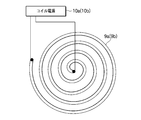
- the top view which shows the induction heating coil used for the apparatus of FIG.
- the flowchart for demonstrating the process at the time of enforcing the film-forming method of the polymeric film which concerns on embodiment of this invention.
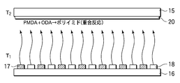
- the schematic diagram for demonstrating the state at the time of forming a polymeric film according to the method which concerns on embodiment of this invention.
- Sectional drawing which shows the film-forming apparatus of the polymeric film which concerns on the 2nd Embodiment of this invention.
- the side view which shows the induction heating coil used for the apparatus of FIG.
- FIG. 1 is a cross-sectional view showing a polymer film forming apparatus according to a first embodiment of the present invention.
- the film forming apparatus 1 has a chamber 2, and a carry-in / out port 3 and an exhaust port 4 are provided on the side wall of the chamber 2.
- the carry-in / out port 3 can be opened and closed by a gate valve 5.
- An exhaust pipe 6 is connected to the exhaust port 4, and a pressure adjustment valve 8 and a vacuum pump 7 are connected to the exhaust pipe 6 to control the opening degree of the pressure adjustment valve 8 while operating the vacuum pump 7.
- the inside of the chamber 2 is adjusted to a predetermined degree of vacuum.
- the pressure in the chamber 2 can be adjusted by introducing an inert gas such as Ar gas into the chamber 2 from a gas supply system (not shown).
- a cleaning gas supply system that supplies a cleaning gas for cleaning the inside of the chamber 2 may be provided.
- the induction heating coils 9a and 9b are provided on the top wall and the bottom wall of the chamber 2, respectively.
- the induction heating coils 9a and 9b have a spiral shape as shown in FIG. 2, and are connected to coil power supplies 10a and 10b, respectively.
- These coil power supplies 10 a and 10 b are connected to the control unit 11 and controlled by the control unit 11.
- the control part 11 controls the heating temperature by the induction heating coils 9a and 9b by controlling the outputs of the coil power supplies 10a and 10b.
- a wall heater (not shown) is provided on the chamber wall, and the temperature of the chamber wall can be controlled to a predetermined temperature.
- Shielding members 12a and 12b that shield them are provided below the induction heating coil 9a and above the induction heating coil 9b.
- the shielding members 12a and 12b are attached to the chamber 2 by the attachment member 13.
- an upper heat transfer plate 14a is provided so as to face the induction heating coil 9a via the shielding member 12a, and a lower part so as to face the induction heating coil 9b via the shielding member 12b.
- a heat transfer plate 14b is provided.
- a deposition target substrate 15 on which a polymer film is to be formed is supported on the upper heat transfer plate 14a by a suitable support means with the film formation surface facing downward, and a polymer film is formed on the lower heat transfer plate 14b.
- a raw material forming substrate 16 having a raw material formed on the upper surface is placed.
- a first raw material 17 and a second raw material 18 for forming a polymer film are formed in a predetermined pattern, for example, a checkered pattern, by coating, printing, photolithography, or the like.
- the first and second raw materials 17 and 18 are monomer raw materials for forming a polymerized film.
- PMDA pyromellitic anhydride
- 4 4 are used as these raw materials.
- ODA '-diaminodiphenyl ether
- the lower heat transfer plate 14b is induction-heated by energizing the induction heating coil 9b, and the raw material forming substrate 16 is heated to the first temperature by the heat transfer, whereby the first raw material 17 and the second heat transfer plate 9b are heated.
- the raw material 18 evaporates.
- the induction heating coil 9a is energized, the upper heat transfer plate 14a is induction-heated, and the film formation substrate 15 is heated to the second temperature by the heat transfer and evaporated on the surface of the film formation substrate 15.
- the first raw material 17 and the second raw material 18 react on the surface of the deposition target substrate 15 to form a polymerized film. That is, the induction heating coil 9b functions as a first heating mechanism that evaporates the raw material, and the induction heating coil 9a functions as a second heating mechanism that causes a polymerization reaction.
- the controller 11 is configured to perform exhaust control, gas supply control, gate valve opening / closing control, substrate transport control, and the like in addition to energization control to the induction heating coils 9a and 9b.
- Computer a user interface including a keyboard and a display on which an operator performs an input operation for control, and a storage unit in which a storage medium in which information for control such as a processing recipe is stored can be set ing.
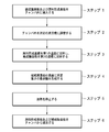
- the gate valve 5 is closed to make the inside of the chamber 2 a sealed space, the inside of the chamber 2 is evacuated by the vacuum pump 7, and an inert gas is introduced into the chamber 2 from a gas introduction mechanism (not shown) as necessary.
- the inside of the chamber 2 is adjusted to a predetermined degree of vacuum (step 2).
- the induction heating coil 9b is energized to inductively heat the lower heat transfer plate 14b, and the raw material forming substrate 16 is heated to the first temperature by the heat transfer, and the induction heating coil 9a is energized to heat the upper heat.
- the transmission plate 14a is induction-heated, and the film formation substrate 15 is heated to the second temperature by the heat transfer (step 3).
- the first temperature is set to a temperature suitable for evaporating the first raw material 17 and the second raw material 18 formed on the raw material formation substrate 16, and the second temperature is set on the deposition target substrate 15.
- the first raw material 17 and the second raw material 18 are set at a temperature suitable for polymerization. Therefore, as shown in FIG. 4, the first raw material 17, for example, PMDA, and the second raw material 18, for example, ODA are transferred from the surface (raw material forming surface) of the raw material forming substrate 16 heated to the first temperature T1.
- the first raw material 17 and the second raw material 18 undergo a polymerization reaction on the surface (deposition surface) of the deposition target substrate 15 which is evaporated and heated to the second temperature T2. Therefore, by continuing such heating for a predetermined time, a polymer film 20 having a predetermined thickness, for example, a polyimide film, is formed on the surface of the deposition target substrate 15 (step 4).
- the first temperature can be set to 200 to 260 ° C.
- the second temperature can be set to 180 to 230 ° C.
- the raw material formation surface of the raw material formation substrate 16 is substantially at the first temperature
- the film formation surface of the film formation substrate 15 is substantially at the second temperature.
- the ratio of the first raw material 17 and the second raw material 18 formed on the raw material forming substrate 16 can be obtained when the stoichiometric composition of the polymer film is obtained when they are evaporated at the first temperature. By setting the ratio, the polymer film 20 having a desired composition can be obtained.
- the first raw material 17 and the second raw material 18 may be formed in such an amount that a polymer film having a desired film thickness is obtained, and the processing may be stopped when all the raw materials are evaporated.
- the raw material forming substrate 16 can also form the first and second raw materials 17 and 18 again after film formation.
- the heating to the induction heating coils 9a and 9b is cut off to stop the heating (step 5), and the gate valve 5 is opened to form the polymer film 20 formed.
- the substrate 15 and the material forming substrate 16 after the material is evaporated are carried out (step 6).
- the chamber 2 may be cleaned with a cleaning gas while the wall surface of the chamber 2 is heated by a wall heater (not shown).
- the first raw material 17 and the second raw material 18 for forming a polymer film are formed in a solid pattern in a predetermined pattern on the raw material forming substrate 16 by coating, printing, photolithography, or the like.
- the raw material forming substrate 16 is heated to a first temperature by induction heating to evaporate these raw materials, and vapor deposition is performed on the surface of the deposition target substrate 15 heated to a second temperature at which a polymerization reaction occurs by induction heating. This causes a polymerization reaction, so there is a problem of heat resistance when supplying high-temperature gas formed by heating the raw material to the pipe, and a problem of instability of raw material supply due to temperature unevenness when heated by a heater.
- a polymer film can be stably formed by a very simple method.
- the raw material forming substrate 16 and the deposition target substrate 15 can be rapidly heated and cooled to independent temperatures by induction heating, the risk of the raw material being supplied at a temperature other than the desired temperature and the polymerization temperature are limited. Can avoid the danger of
- a pancake type is used as the induction heating coils 9a and 9b, and a graphite plate having a diameter of 210 mm and a thickness of 2 mm is used as the upper heat transfer plate 14a and the lower heat transfer plate 14b.
- An Ar gas supply system, a cleaning gas supply system, and a wall heater were provided.
- a 200 mm Si wafer is used as the film formation substrate 15, a PMDA is used as the first material 17, and ODA is used as the second material 18 on the surface of the 200 mm Si wafer as the material forming substrate 16 by a printing method. And a 1 ⁇ m space was used to form a checkered pattern.
- the film was formed by the following flow. First, in a state where the induction heating coils 9a and 9b are not energized, the deposition target substrate 15 is set on the upper heat transfer plate 14a and the raw material forming substrate 16 is set on the lower heat transfer plate 14b. Next, after the chamber 2 is evacuated, the pressure in the chamber 2 is adjusted to 133 Pa.
- the control unit 11 induction-heats the lower heat transfer plate 14b while controlling energization to the induction heating coil 9b, controls the temperature of the raw material forming substrate 16 to 220 ° C., and supplies the induction heating coil 9a to the induction heating coil 9a.
- the upper heat transfer plate 14a is induction-heated while controlling energization, and the temperature of the film formation substrate 15 is controlled to 200 ° C.
- PMDA and ODA evaporate from the raw material forming substrate 16, a polymerization reaction occurs on the surface of the deposition target substrate 15, and a polyimide film is formed.
- a polyimide film having a thickness of 1000 nm was obtained by continuing heating at the above temperature for 5 minutes.
- the energization of the induction heating coils 9a and 9b is stopped, and the interior of the chamber 2 is purged with Ar gas to return to atmospheric pressure.
- the film formation substrate 15 and the raw material formation substrate 16 that have been formed are carried out of the chamber 2.
- the temperature of the wall of the chamber 2 is controlled to 500 ° C. by a wall heater, and an oxygen source such as O 2 , O 3 , or N 2 O as a cleaning gas is supplied into the chamber 2 from the cleaning gas supply system. Supply and clean the inside of the chamber 2.
- an oxygen source such as O 2 , O 3 , or N 2 O as a cleaning gas is supplied into the chamber 2 from the cleaning gas supply system. Supply and clean the inside of the chamber 2.
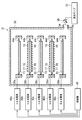
- FIG. 5 is a sectional view showing a polymer film forming apparatus according to the second embodiment of the present invention.
- the film forming apparatus 31 has a chamber 32, and a plurality of loading / unloading ports (not shown) and one exhaust port 34 are provided on the side wall of the chamber 32.
- the loading / unloading port is for loading and unloading a plurality of substrates, and can be opened and closed by a gate valve (not shown).
- An exhaust pipe 36 is connected to the exhaust port 34, and a pressure adjustment valve 38 and a vacuum pump 37 are connected to the exhaust pipe 36, and the opening degree of the pressure adjustment valve 38 is controlled while operating the vacuum pump 37.
- the pressure in the chamber 32 can be adjusted by introducing an inert gas such as Ar gas into the chamber 32 from a gas supply system (not shown).
- a cleaning gas supply system that supplies a cleaning gas for cleaning the inside of the chamber 32 may be provided.
- heat transfer plates 44a, 44b, 44c, 44d, and 44e are provided so as to be stacked horizontally and vertically.
- Inductive heating coils 39a, 39b, 39c, 39d, and 39e are provided on the outer peripheries of these heat transfer plates, respectively.
- Coil power sources 40a, 40b, 40c, 40d, and 40e are connected to the induction heating coils 39a, 39b, 39c, 39d, and 39e, respectively.
- These coil power sources 40a, 40b, 40c, 40d, and 40e are connected to the control unit 41. Connected and controlled by the control unit 41.
- control part 41 controls the heating temperature by the induction heating coils 39a, 39b, 39c, 39d, 39e by controlling the outputs of the coil power sources 40a, 40b, 40c, 40d, 40e. Further, a wall heater (not shown) is provided on the chamber wall, and the temperature of the chamber wall can be controlled to a predetermined temperature.
- the control unit 41 is configured in the same manner as in the first embodiment 11, and can perform the same control.
- the induction heating coil 39a is provided so that the outer periphery of the heat-transfer board 44a may be wound, as shown in FIG.
- the induction heating coils 39b, 39c, 39d, and 39e are configured similarly to the induction heating coil 39a.
- a film formation substrate 15 on which a polymer film is to be formed is supported on the lower surface of the uppermost heat transfer plate 44a with the film formation surface facing downward.
- the lower heat transfer plate 44b supports a raw material forming substrate 16 on which raw materials for forming a polymer film are formed on the upper and lower surfaces thereof.
- the deposition substrate 15 on which a polymer film is to be formed is supported on the upper and lower surfaces of the heat transfer plate 44c below.
- the raw material forming substrate 16 on which the raw material for forming the polymer film is formed on the upper and lower surfaces of the heat transfer plate 44d below is supported.
- a deposition target substrate 15 on which a polymer film is to be deposited is supported on the upper surface of the lowermost heat transfer plate 44e with the deposition surface facing upward.
- the first raw material 17 and the second raw material 18 for forming the polymer film are formed on the raw material forming substrate 16 by a predetermined pattern, such as a checkered pattern, by coating, printing, photolithography, or the like. Is formed.
- the film formation substrate 15 and the raw material formation substrate 16 By disposing the film formation substrate 15 and the raw material formation substrate 16 as described above, between the heat transfer plates 44a and 44b, between the heat transfer plates 44b and 44c, between the heat transfer plates 44c and 44d, The film formation substrate 15 and the raw material formation substrate 16 can be provided between the heat transfer plates 44d and 44e so that the film formation surface and the raw material formation surface face each other. Therefore, by energizing the dielectric heating coils 39b and 39d to inductively heat the heat transfer plates 44b and 44d, the raw material forming substrate 16 is heated to the first temperature by the heat transfer, and the dielectric heating coils 39a, 39c and 39e.
- the first raw material evaporated from the raw material forming substrate 16 by inductively heating the heat transfer plates 44a, 44c, and 44e to heat the deposition target substrate 15 to the second temperature by the heat transfer. 17 and the second raw material 18 can reach the film formation surface of the deposition target substrate 15 facing each other, and these raw materials react on the film formation surface to form a polymerized film. That is, the induction heating coils 39b and 39d function as a first heating mechanism that evaporates the raw material, and the induction heating coils 39a, 39c, and 39e function as a second heating mechanism that causes a polymerization reaction.
- the first raw material 17 and the second raw material are monomer raw materials for forming a polymer film, and when the polymer film to be obtained is polyimide, pyromellitic anhydride is used as the raw material.
- a polymer film can be formed basically in the same manner as in the first embodiment, but a polymer film is formed on four substrates 15 at a time. Therefore, it is more efficient than the first embodiment.
- a graphite plate having a diameter of 210 mm and a thickness of 2 mm is used as the heat transfer plates 44a to 44e, and an Ar gas supply system, a cleaning gas supply system, and a wall heater (not shown) are provided.
- a 200 mm Si wafer is used as the film formation substrate 15, and the raw material formation substrate 16 is printed on the surface of the 200 mm Si wafer by a printing method, PMDA as the first material 17, and ODA as the second material 18, each in a 5 ⁇ m square. Films were formed using a checkered pattern with a 1 ⁇ m space.
- the pressure in the chamber 32 is adjusted to 133 Pa, the temperature of the raw material substrate 16 is controlled to 220 ° C., and the temperature of the deposition target substrate 15 is controlled to 200 ° C. By continuing such heating for 5 minutes, a polyimide film having a thickness of 5 nm was obtained.
- the induction heating coils 39 a to 39 e are present in the processing space of the chamber 32, but may be present outside the chamber 32.
- the present invention is not limited thereto, and an arbitrary number of film formation substrates can be formed by appropriately adjusting the number of heat transfer plates.
- a polymerized film can be formed on the film substrate 15.
- a first substrate having a plurality of raw materials for forming a polymer film formed on a raw material forming surface in a solid pattern in a predetermined pattern, and a film forming surface on which a polymer film is to be formed.
- Two substrates are provided opposite to each other in the processing container so that the raw material formation surface and the film formation surface face each other, and the first substrate and the second substrate are independently set at a desired temperature.
- the plurality of raw materials evaporated from the first substrate are reacted on the film formation surface of the second substrate to form a predetermined polymerized film on the film formation surface.
- a polymerized film can be formed.
- a heating mechanism capable of rapid heating and rapid cooling such as induction heating, there is a risk of the raw material being supplied at a temperature other than the desired temperature, polymerization The danger that the temperature is limited can be avoided.
- the present invention is not limited to the above embodiment and can be variously modified.
- the film forming apparatus is not limited to the one used in the first and second embodiments, and may have another apparatus configuration.
- an induction heating coil capable of rapid heating and rapid cooling was used, but not limited to this, other heating means such as lamp heating May be used.
- the polymer film is formed using the first raw material and the second raw material has been described, but the polymer film may be formed using three or more raw materials.
- a polyimide film is formed using PMDA and ODA as raw materials monomers is not limited to this, but perylene tetracarboxylic dianhydride (PTCDA) and 2,3-diaminonaphthalene are used.
- the present invention is not limited to this.
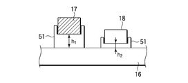
- the heat conduction adjusting jig 51 having a relatively large heat insulating property is provided, and the first raw material 17 and the second raw material 18 are formed thereon, and the heat conduction is adjusted by the first raw material 17 and the second raw material 18.
- the heating temperature of the first raw material and the second raw material can be made different by adjusting the height of the jig 51 to h1 and h2, respectively, to adjust the heat conduction.
- the method for forming a polymer film according to the present invention can be suitably used for forming a high-performance polymer film used for a three-dimensional mounting insulating film or the like used in the semiconductor field.
Landscapes
- Chemical & Material Sciences (AREA)
- Health & Medical Sciences (AREA)
- Chemical Kinetics & Catalysis (AREA)
- Medicinal Chemistry (AREA)
- Polymers & Plastics (AREA)
- Organic Chemistry (AREA)
- Physical Vapour Deposition (AREA)
- Formation Of Insulating Films (AREA)
- Macromolecular Compounds Obtained By Forming Nitrogen-Containing Linkages In General (AREA)
Priority Applications (3)
| Application Number | Priority Date | Filing Date | Title |
|---|---|---|---|
| CN2009801363461A CN102160156B (zh) | 2008-09-16 | 2009-07-17 | 聚合膜的成膜方法和成膜装置 |
| KR1020117006035A KR101236160B1 (ko) | 2008-09-16 | 2009-07-17 | 중합막의 성막 방법 및 성막 장치 |
| US13/063,779 US8691338B2 (en) | 2008-09-16 | 2009-07-17 | Polymerized film forming method and polymerized film forming apparatus |
Applications Claiming Priority (2)
| Application Number | Priority Date | Filing Date | Title |
|---|---|---|---|
| JP2008236819A JP5292032B2 (ja) | 2008-09-16 | 2008-09-16 | 重合膜の成膜方法および成膜装置 |
| JP2008-236819 | 2008-09-16 |
Publications (1)
| Publication Number | Publication Date |
|---|---|
| WO2010032547A1 true WO2010032547A1 (ja) | 2010-03-25 |
Family
ID=42039389
Family Applications (1)
| Application Number | Title | Priority Date | Filing Date |
|---|---|---|---|
| PCT/JP2009/062956 Ceased WO2010032547A1 (ja) | 2008-09-16 | 2009-07-17 | 重合膜の成膜方法および成膜装置 |
Country Status (5)
| Country | Link |
|---|---|
| US (1) | US8691338B2 (enExample) |
| JP (1) | JP5292032B2 (enExample) |
| KR (1) | KR101236160B1 (enExample) |
| CN (1) | CN102160156B (enExample) |
| WO (1) | WO2010032547A1 (enExample) |
Cited By (2)
| Publication number | Priority date | Publication date | Assignee | Title |
|---|---|---|---|---|
| US20120269970A1 (en) * | 2011-03-29 | 2012-10-25 | Tokyo Electron Limited | Cleaning method and film depositing method |
| CN120683456A (zh) * | 2025-08-25 | 2025-09-23 | 浙江晟霖益嘉科技有限公司 | 一种双晶圆处理腔及其控制方法 |
Families Citing this family (9)
| Publication number | Priority date | Publication date | Assignee | Title |
|---|---|---|---|---|
| JP2014005478A (ja) * | 2010-10-08 | 2014-01-16 | Kaneka Corp | 蒸着装置 |
| US20140014036A1 (en) * | 2011-03-30 | 2014-01-16 | Sharp Kabushiki Kaisha | Deposition particle emitting device, deposition particle emission method, and deposition device |
| JP6224479B2 (ja) * | 2014-02-18 | 2017-11-01 | 東京エレクトロン株式会社 | 重合膜の成膜方法および成膜装置 |
| CN106555159B (zh) * | 2015-09-28 | 2018-12-11 | 北京北方华创微电子装备有限公司 | 一种基片的加热设备及加热方法 |
| JP6851171B2 (ja) * | 2016-10-14 | 2021-03-31 | 株式会社アルバック | 微細機能素子及び微細機能素子の製造方法 |
| KR102120537B1 (ko) * | 2017-04-02 | 2020-06-09 | 황창훈 | 고해상도 oled 소자 제작용 면증발원 동시증발 증착공정방법 |
| CN108570645B (zh) * | 2017-11-30 | 2023-09-29 | 上海微电子装备(集团)股份有限公司 | 真空蒸镀装置及其蒸发头、真空蒸镀方法 |
| JP6799550B2 (ja) * | 2018-01-16 | 2020-12-16 | 東京エレクトロン株式会社 | プラズマ処理装置の部品をクリーニングする方法 |
| JP7236953B2 (ja) * | 2019-08-05 | 2023-03-10 | 東京エレクトロン株式会社 | 成膜装置および成膜方法 |
Citations (3)
| Publication number | Priority date | Publication date | Assignee | Title |
|---|---|---|---|---|
| JPH09326388A (ja) * | 1996-06-05 | 1997-12-16 | Ulvac Japan Ltd | 低比誘電率高分子膜の形成方法及び層間絶縁膜の形成方法並びに低比誘電率高分子膜形成装置 |
| JP2001011176A (ja) * | 1999-06-25 | 2001-01-16 | Matsushita Electric Works Ltd | ポリイミド皮膜の形成方法及びポリイミド皮膜 |
| JP2002285320A (ja) * | 2001-03-27 | 2002-10-03 | Fukushima Prefecture | 有機高分子薄膜の形成方法 |
Family Cites Families (8)
| Publication number | Priority date | Publication date | Assignee | Title |
|---|---|---|---|---|
| JP3231373B2 (ja) | 1991-12-20 | 2001-11-19 | 松下電器産業株式会社 | 合成樹脂被膜の形成装置及び形成方法 |
| US5937272A (en) * | 1997-06-06 | 1999-08-10 | Eastman Kodak Company | Patterned organic layers in a full-color organic electroluminescent display array on a thin film transistor array substrate |
| KR100680863B1 (ko) * | 2003-02-04 | 2007-02-09 | 동경 엘렉트론 주식회사 | 처리시스템 및 이 처리시스템의 가동방법 |
| JP4257576B2 (ja) * | 2003-03-25 | 2009-04-22 | ローム株式会社 | 成膜装置 |
| WO2005109486A1 (en) * | 2004-05-12 | 2005-11-17 | Viatron Technologies Inc. | System for heat treatment of semiconductor device |
| JP2006351814A (ja) | 2005-06-15 | 2006-12-28 | Tokyo Electron Ltd | クリーニング方法、コンピュータプログラム及び成膜装置 |
| WO2008069259A1 (en) * | 2006-12-05 | 2008-06-12 | Semiconductor Energy Laboratory Co., Ltd. | Film formation apparatus, film formation method, manufacturing apparatus, and method for manufacturing light-emitting device |
| KR20090028413A (ko) * | 2007-09-13 | 2009-03-18 | 가부시키가이샤 한도오따이 에네루기 켄큐쇼 | 발광장치 제작방법 및 증착용 기판 |
-
2008
- 2008-09-16 JP JP2008236819A patent/JP5292032B2/ja not_active Expired - Fee Related
-
2009
- 2009-07-17 CN CN2009801363461A patent/CN102160156B/zh not_active Expired - Fee Related
- 2009-07-17 WO PCT/JP2009/062956 patent/WO2010032547A1/ja not_active Ceased
- 2009-07-17 US US13/063,779 patent/US8691338B2/en not_active Expired - Fee Related
- 2009-07-17 KR KR1020117006035A patent/KR101236160B1/ko not_active Expired - Fee Related
Patent Citations (3)
| Publication number | Priority date | Publication date | Assignee | Title |
|---|---|---|---|---|
| JPH09326388A (ja) * | 1996-06-05 | 1997-12-16 | Ulvac Japan Ltd | 低比誘電率高分子膜の形成方法及び層間絶縁膜の形成方法並びに低比誘電率高分子膜形成装置 |
| JP2001011176A (ja) * | 1999-06-25 | 2001-01-16 | Matsushita Electric Works Ltd | ポリイミド皮膜の形成方法及びポリイミド皮膜 |
| JP2002285320A (ja) * | 2001-03-27 | 2002-10-03 | Fukushima Prefecture | 有機高分子薄膜の形成方法 |
Cited By (2)
| Publication number | Priority date | Publication date | Assignee | Title |
|---|---|---|---|---|
| US20120269970A1 (en) * | 2011-03-29 | 2012-10-25 | Tokyo Electron Limited | Cleaning method and film depositing method |
| CN120683456A (zh) * | 2025-08-25 | 2025-09-23 | 浙江晟霖益嘉科技有限公司 | 一种双晶圆处理腔及其控制方法 |
Also Published As
| Publication number | Publication date |
|---|---|
| US20110171384A1 (en) | 2011-07-14 |
| KR101236160B1 (ko) | 2013-02-22 |
| KR20110051250A (ko) | 2011-05-17 |
| US8691338B2 (en) | 2014-04-08 |
| JP5292032B2 (ja) | 2013-09-18 |
| CN102160156A (zh) | 2011-08-17 |
| CN102160156B (zh) | 2013-04-17 |
| JP2010073743A (ja) | 2010-04-02 |
Similar Documents
| Publication | Publication Date | Title |
|---|---|---|
| JP5292032B2 (ja) | 重合膜の成膜方法および成膜装置 | |
| KR102493002B1 (ko) | 증착 내내 웨이퍼 온도를 가변함으로써 계면 반응들 억제 | |
| KR102664066B1 (ko) | 유기막들의 기상 퇴적 | |
| JP5243519B2 (ja) | 成膜装置 | |
| US20220323991A1 (en) | Vapor phase deposition of organic films | |
| JP5862459B2 (ja) | 成膜方法 | |
| KR101994874B1 (ko) | 건조 장치 및 건조 처리 방법 | |
| JP5604289B2 (ja) | 成膜装置 | |
| KR101243397B1 (ko) | 기판 가열 장치 및 기판 가열 방법 및 기판 처리 시스템 | |
| KR20100102228A (ko) | 성막 장치 및, 성막 방법 | |
| KR101041143B1 (ko) | 기판 가공 장치 | |
| WO2014062619A1 (en) | Apparatus and method for heat treatment of coatings on substrates | |
| TWI751173B (zh) | 用於由微波固化調整聚合物之熱膨脹係數(cte)的方法 | |
| JP2015173226A (ja) | 真空成膜装置及びこの装置を用いた成膜方法 | |
| JPH10289902A (ja) | 成膜装置 | |
| JP3806660B2 (ja) | 減圧乾燥装置及び減圧乾燥方法 | |
| JP3766336B2 (ja) | 減圧乾燥装置及び減圧乾燥方法 | |
| JP5358201B2 (ja) | 成膜方法 | |
| WO2006135007A1 (ja) | 成膜およびクリーニング方法 | |
| KR20190057468A (ko) | 서브 챔버를 구비한 iCVD 시스템 및 방법 | |
| JP2011009380A (ja) | 成膜装置 | |
| JP2011021264A (ja) | 成膜装置 |
Legal Events
| Date | Code | Title | Description |
|---|---|---|---|
| WWE | Wipo information: entry into national phase |
Ref document number: 200980136346.1 Country of ref document: CN |
|
| 121 | Ep: the epo has been informed by wipo that ep was designated in this application |
Ref document number: 09814392 Country of ref document: EP Kind code of ref document: A1 |
|
| WWE | Wipo information: entry into national phase |
Ref document number: 13063779 Country of ref document: US |
|
| ENP | Entry into the national phase |
Ref document number: 20117006035 Country of ref document: KR Kind code of ref document: A |
|
| NENP | Non-entry into the national phase |
Ref country code: DE |
|
| 122 | Ep: pct application non-entry in european phase |
Ref document number: 09814392 Country of ref document: EP Kind code of ref document: A1 |