WO2010029645A1 - 不揮発性記憶装置及びその製造方法 - Google Patents
不揮発性記憶装置及びその製造方法 Download PDFInfo
- Publication number
- WO2010029645A1 WO2010029645A1 PCT/JP2008/066603 JP2008066603W WO2010029645A1 WO 2010029645 A1 WO2010029645 A1 WO 2010029645A1 JP 2008066603 W JP2008066603 W JP 2008066603W WO 2010029645 A1 WO2010029645 A1 WO 2010029645A1
- Authority
- WO
- WIPO (PCT)
- Prior art keywords
- layer
- electrode
- memory device
- nonvolatile memory
- valence
- Prior art date
- Legal status (The legal status is an assumption and is not a legal conclusion. Google has not performed a legal analysis and makes no representation as to the accuracy of the status listed.)
- Ceased
Links
Images







Classifications
-
- B—PERFORMING OPERATIONS; TRANSPORTING
- B82—NANOTECHNOLOGY
- B82Y—SPECIFIC USES OR APPLICATIONS OF NANOSTRUCTURES; MEASUREMENT OR ANALYSIS OF NANOSTRUCTURES; MANUFACTURE OR TREATMENT OF NANOSTRUCTURES
- B82Y10/00—Nanotechnology for information processing, storage or transmission, e.g. quantum computing or single electron logic
-
- G—PHYSICS
- G11—INFORMATION STORAGE
- G11B—INFORMATION STORAGE BASED ON RELATIVE MOVEMENT BETWEEN RECORD CARRIER AND TRANSDUCER
- G11B9/00—Recording or reproducing using a method not covered by one of the main groups G11B3/00 - G11B7/00; Record carriers therefor
- G11B9/04—Recording or reproducing using a method not covered by one of the main groups G11B3/00 - G11B7/00; Record carriers therefor using record carriers having variable electric resistance; Record carriers therefor
-
- G—PHYSICS
- G11—INFORMATION STORAGE
- G11C—STATIC STORES
- G11C13/00—Digital stores characterised by the use of storage elements not covered by groups G11C11/00, G11C23/00, or G11C25/00
- G11C13/0002—Digital stores characterised by the use of storage elements not covered by groups G11C11/00, G11C23/00, or G11C25/00 using resistive RAM [RRAM] elements
- G11C13/0007—Digital stores characterised by the use of storage elements not covered by groups G11C11/00, G11C23/00, or G11C25/00 using resistive RAM [RRAM] elements comprising metal oxide memory material, e.g. perovskites
-
- H—ELECTRICITY
- H10—SEMICONDUCTOR DEVICES; ELECTRIC SOLID-STATE DEVICES NOT OTHERWISE PROVIDED FOR
- H10B—ELECTRONIC MEMORY DEVICES
- H10B63/00—Resistance change memory devices, e.g. resistive RAM [ReRAM] devices
- H10B63/20—Resistance change memory devices, e.g. resistive RAM [ReRAM] devices comprising selection components having two electrodes, e.g. diodes
-
- H—ELECTRICITY
- H10—SEMICONDUCTOR DEVICES; ELECTRIC SOLID-STATE DEVICES NOT OTHERWISE PROVIDED FOR
- H10B—ELECTRONIC MEMORY DEVICES
- H10B63/00—Resistance change memory devices, e.g. resistive RAM [ReRAM] devices
- H10B63/80—Arrangements comprising multiple bistable or multi-stable switching components of the same type on a plane parallel to the substrate, e.g. cross-point arrays
-
- H—ELECTRICITY
- H10—SEMICONDUCTOR DEVICES; ELECTRIC SOLID-STATE DEVICES NOT OTHERWISE PROVIDED FOR
- H10B—ELECTRONIC MEMORY DEVICES
- H10B63/00—Resistance change memory devices, e.g. resistive RAM [ReRAM] devices
- H10B63/80—Arrangements comprising multiple bistable or multi-stable switching components of the same type on a plane parallel to the substrate, e.g. cross-point arrays
- H10B63/84—Arrangements comprising multiple bistable or multi-stable switching components of the same type on a plane parallel to the substrate, e.g. cross-point arrays arranged in a direction perpendicular to the substrate, e.g. 3D cell arrays
-
- H—ELECTRICITY
- H10—SEMICONDUCTOR DEVICES; ELECTRIC SOLID-STATE DEVICES NOT OTHERWISE PROVIDED FOR
- H10N—ELECTRIC SOLID-STATE DEVICES NOT OTHERWISE PROVIDED FOR
- H10N70/00—Solid-state devices having no potential barriers, and specially adapted for rectifying, amplifying, oscillating or switching
- H10N70/20—Multistable switching devices, e.g. memristors
- H10N70/24—Multistable switching devices, e.g. memristors based on migration or redistribution of ionic species, e.g. anions, vacancies
-
- H—ELECTRICITY
- H10—SEMICONDUCTOR DEVICES; ELECTRIC SOLID-STATE DEVICES NOT OTHERWISE PROVIDED FOR
- H10N—ELECTRIC SOLID-STATE DEVICES NOT OTHERWISE PROVIDED FOR
- H10N70/00—Solid-state devices having no potential barriers, and specially adapted for rectifying, amplifying, oscillating or switching
- H10N70/801—Constructional details of multistable switching devices
- H10N70/821—Device geometry
- H10N70/826—Device geometry adapted for essentially vertical current flow, e.g. sandwich or pillar type devices
-
- H—ELECTRICITY
- H10—SEMICONDUCTOR DEVICES; ELECTRIC SOLID-STATE DEVICES NOT OTHERWISE PROVIDED FOR
- H10N—ELECTRIC SOLID-STATE DEVICES NOT OTHERWISE PROVIDED FOR
- H10N70/00—Solid-state devices having no potential barriers, and specially adapted for rectifying, amplifying, oscillating or switching
- H10N70/801—Constructional details of multistable switching devices
- H10N70/841—Electrodes
-
- H—ELECTRICITY
- H10—SEMICONDUCTOR DEVICES; ELECTRIC SOLID-STATE DEVICES NOT OTHERWISE PROVIDED FOR
- H10N—ELECTRIC SOLID-STATE DEVICES NOT OTHERWISE PROVIDED FOR
- H10N70/00—Solid-state devices having no potential barriers, and specially adapted for rectifying, amplifying, oscillating or switching
- H10N70/801—Constructional details of multistable switching devices
- H10N70/881—Switching materials
- H10N70/883—Oxides or nitrides
- H10N70/8836—Complex metal oxides, e.g. perovskites, spinels
-
- G—PHYSICS
- G11—INFORMATION STORAGE
- G11C—STATIC STORES
- G11C2213/00—Indexing scheme relating to G11C13/00 for features not covered by this group
- G11C2213/30—Resistive cell, memory material aspects
- G11C2213/32—Material having simple binary metal oxide structure
-
- G—PHYSICS
- G11—INFORMATION STORAGE
- G11C—STATIC STORES
- G11C2213/00—Indexing scheme relating to G11C13/00 for features not covered by this group
- G11C2213/30—Resistive cell, memory material aspects
- G11C2213/34—Material includes an oxide or a nitride
-
- G—PHYSICS
- G11—INFORMATION STORAGE
- G11C—STATIC STORES
- G11C2213/00—Indexing scheme relating to G11C13/00 for features not covered by this group
- G11C2213/50—Resistive cell structure aspects
- G11C2213/52—Structure characterized by the electrode material, shape, etc.
-
- G—PHYSICS
- G11—INFORMATION STORAGE
- G11C—STATIC STORES
- G11C2213/00—Indexing scheme relating to G11C13/00 for features not covered by this group
- G11C2213/70—Resistive array aspects
- G11C2213/71—Three dimensional array
Definitions
- the present invention relates to a nonvolatile memory device and a manufacturing method thereof.
- NAND flash memory and small HDD hard disk drive
- NAND flash memory and small HDD have made rapid progress in recording density, and are used in various applications such as portable music market, portable game recording memory, and personal computer storage devices. It has been.
- these non-volatile memories have a limit of high density.
- an electrode for supplying a current to the resistance variable material to be a memory layer is provided.
- the electrode on the side where current flows into the memory layer is oxidized, and a high resistance layer is formed at the interface of this electrode, particularly in contact with the memory layer.
- This high resistance layer makes the operation of the ReRAM unstable and increases the power consumption.For example, the Joule heat generated at the time of resetting when a large current is applied is increased, causing further oxidation and extending the life of the ReRAM. It will shrink.
- Patent Document 1 discloses a technique in which a nitride or oxide such as TiN or ZnO is used as an electrode in contact with a metal oxide layer whose resistance is changed by an electric signal.
- JP 2007-42784 A JP 2007-42784 A
- the present invention provides a nonvolatile memory device that suppresses electrode deterioration and has a long operating life and a method for manufacturing the same.
- an electrode includes a storage layer connected to the electrode and having a resistance that is changed by a current flowing from the electrode.
- the electrode includes a metal element and a first valence n.
- a first layer containing a first non-metallic element, and a second valence that is provided between the first layer and the memory layer, and the metal element and a second valence that is one greater than the first valence n There is provided a non-volatile memory device including a second layer including a second non-metallic element having n + 1).
- a method for manufacturing a nonvolatile memory device having a stacked structure including an electrode and a memory layer whose resistance is changed by a current flowing from the electrode, Forming a first layer film having a metal element and a first non-metallic element having a first valence n, which are a part of the electrode, and another part of the electrode and the memory layer Forming a second layer film having the metal element and a second non-metal element having a second valence (n + 1) that is one greater than the first valence n;
- a method for manufacturing a nonvolatile memory device is provided.
- FIG. 1 is a schematic view illustrating the configuration of a nonvolatile memory device according to a first embodiment of the invention.
- 1 is a schematic view illustrating the configuration of a nonvolatile memory device according to a first embodiment of the invention.
- FIG. 6 is a schematic perspective view illustrating the configuration of another nonvolatile memory device according to the first embodiment of the invention.
- FIG. 3 is a schematic perspective view illustrating the state of the electrode surface in the nonvolatile memory device according to the first embodiment of the invention.
- FIG. 6 is a schematic cross-sectional view illustrating the operation in the nonvolatile memory device according to the first embodiment of the invention. It is a typical perspective view which illustrates the state of the electrode surface in the non-volatile memory device of a comparative example.
- FIG. 6 is a schematic cross-sectional view illustrating the operation in a nonvolatile memory device of a comparative example.
- FIG. FIG. 6 is a flowchart illustrating a method for manufacturing a nonvolatile memory device according to a second embodiment of the invention.
- 6 is a schematic cross-sectional view in order of the processes, illustrating the method for manufacturing the nonvolatile memory device according to the second embodiment of the invention.
- FIG. FIG. 10 is a schematic cross-sectional view in order of the processes following FIG. 9.
- FIG. 6 is a schematic perspective view illustrating the configuration of a nonvolatile memory device according to a third embodiment of the invention.
- FIG. 7 is a schematic plan view illustrating the configuration of a nonvolatile memory device according to a third embodiment of the invention.
- Nonvolatile memory device 101 Voltage application unit 105 Substrate 110 First wiring 110f First conductive film 120 Second wiring 120f Second conductive film 130 Intersection 140 Storage unit 141 First electrode 141a First layer 141af First layer film 141b Second layer 141bf Second layer film 141p Oxide layer 142 Memory layer 142f Memory layer film 143 Second electrode 143f Second electrode film 145 Multilayer structure 150 Rectifier element section 150f Rectifier element section film 160 Insulating part 160f Insulating part film 201 Metal element 202 First nonmetallic element 203 Second nonmetallic element 205 Lattice defect 206 First lattice defect (cation vacancy) 207 Second lattice defect (anion vacancies) 515 Driver 516 XY scanner 520 523 Substrate 521 Conductive layer 522 Storage unit 524 Probe 525 526 Multiplex driver
- FIG. 1 is a schematic view illustrating the configuration of a nonvolatile memory device according to the first embodiment of the invention.
- 1A is a schematic perspective view of the main part
- FIG. 1B is a cross-sectional view taken along the line AA ′ of FIG. 1C
- FIG. It is B 'sectional view.
- FIG. 2 is a schematic view illustrating the configuration of the nonvolatile memory device according to the first embodiment of the invention.
- 1A is a schematic perspective view
- FIG. 1B is a plan view.
- FIG. 3 is a schematic perspective view illustrating the configuration of another nonvolatile memory device according to the first embodiment of the invention.
- the nonvolatile memory device according to the first embodiment is a cross-point nonvolatile memory device.
- a strip shape extending in the X-axis direction on the main surface of the substrate 105.
- the first wiring 110 is provided.
- a band-like second wiring 120 extending in the Y-axis direction orthogonal to the X-axis in a plane parallel to the substrate 105 is provided to face the first wiring 110.
- the first wiring 110 and the second wiring 120 are orthogonal to each other; however, the first wiring 110 and the second wiring 120 may be crossed (non-parallel).
- the plane parallel to the main surface of the substrate 105 is defined as the XY plane
- the extending direction of the first wiring 110 is defined as the X axis
- the axis is the Y axis
- the direction perpendicular to the X axis and the Y axis is the Z axis.
- first wiring 110 and the second wiring 120 show an example in which four first wirings 110 and four second wirings 120 are provided.
- the present invention is not limited to this.
- the number of the first wiring 110 and the second wiring 120 is arbitrary.
- the first wiring 110 becomes a bit wiring (BL)
- the second wiring 120 becomes a word line (WL).
- the first wiring 110 may be a word line (WL)
- the second wiring 120 may be a bit line (BL).
- BL bit wiring
- WL word line
- the storage unit 140 is sandwiched between the first wiring 110 and the second wiring 120. That is, in the nonvolatile memory device 10, the storage unit 140 is provided at an intersection 130 (cross point) formed by three-dimensionally intersecting bit lines and word lines.
- the storage unit 140 includes a first electrode (electrode) 141, a second electrode 143, and a storage layer 142 provided between the first electrode 141 and the second electrode 143.
- a structure 145 is included.
- the memory layer 142 has, for example, nickel oxide (NiO x ), titanium oxide (TiO x ), ZnMn 2 O 4 , Pr x Ca 1-x MnO whose electric resistance value changes when a voltage is applied and a current flows. 3 etc. can be used. Further, the memory layer 142 includes an oxide containing at least one selected from the group consisting of Ti, Ta, Zr, Hf, W, Mo, Ni, Er, Mn, Ir, Nb, Sr, and Ce. Can be included. However, the present invention is not limited to this, and any material that exhibits a resistance change when a voltage flows and a current flows can be used for the memory layer 142.
- each storage unit 140 (each stacked structure 145) varies depending on the combination of the potential applied to the first wiring 110 and the potential applied to the second wiring 120, and the characteristics of the storage unit 140 at that time are changed. Can store information.
- a rectifying element unit 150 having a rectifying characteristic can be provided.
- the rectifying element unit 150 for example, a PIN diode, an MIM (Metal-Insulator-Metal) element, or the like can be used.
- the rectifying element portion 150 may be provided in a region other than a region where the first wiring 110 and the second wiring 120 face each other. In the case where the storage unit 140 (laminated structure 145) and the rectifying element unit 150 are provided between the first wiring 110 and the second wiring 120, the stacking order of the storage unit 140 and the rectifying element unit 150 is arbitrary. .
- the stacking order of the storage unit 140 and the rectifying element unit 150 is as follows.
- the stacking order of the storage unit 140 and the rectifying element unit 150 may be the same or may be changed.
- a silicon substrate can be used, and a driving circuit for driving a nonvolatile memory device can be provided.
- Various conductive materials containing a metal element can be used for the first wiring 110 and the second wiring 120.
- the first wiring 110 and the second wiring 120 are stored in a region formed by three-dimensionally intersecting with each other.
- the unit 140 is provided, and this one storage unit 140 is one element and is called a cell.
- the first wiring 110, the second wiring 120, and the storage unit 140 have a plurality of regions provided at intervals.
- the insulating portion 160 is provided so as to be sandwiched between the plurality of regions.
- the insulating portion 160 is omitted.
- silicon oxide (SiO 2 ) having a high electric resistance can be used for these insulating portions 160.
- the present invention is not limited thereto, and various materials higher than the electric resistance of the storage unit 140 can be used for the insulating unit 160.
- At least one of the first electrode 141 and the second electrode 143 may be shared by either the first wiring 110 or the second wiring 120.
- at least one of the first electrode 141 and the second electrode 143 may be shared by, for example, a part of the conductive layer that becomes the rectifying element unit 150.
- the nonvolatile memory device 10 stores data by applying a voltage to the stacked structure 145 including the electrode (first electrode 141) and the memory layer 142 and applying a current to the memory layer 142.
- the voltage application unit 101 that is, the first wiring 110 and the second wiring 120 that stores information by causing a resistance change in the layer 142 is provided.
- the nonvolatile memory device according to this embodiment includes a two-layer stacked structure like the nonvolatile memory device 20 illustrated in FIG. 3A and the nonvolatile memory device 21 illustrated in FIG. In addition to such a four-layer structure, it may have a larger number of layer structures.
- the nonvolatile memory device 10 illustrated in FIGS. 1 and 2 will be described as an example of the nonvolatile memory device according to the present embodiment.
- the nonvolatile memory device 10 it is assumed that a current is passed from the first electrode (electrode) 141 toward the second electrode 143. That is, the first electrode 141 conducts a current from the first electrode 141 toward the memory layer 142.
- the first electrode 141 includes the first layer 141a and the second layer 141b provided between the first layer 141a and the memory layer 142.
- the first electrode 141 includes a metal element and a first nonmetal element having a first valence n.
- the first electrode 141 includes a second layer 141b provided at the interface with the memory layer 142, and the second layer 141b has a valence (absolute value) higher than that of the metal element and the first nonmetal element. Includes one larger non-metallic element.
- the second layer 141b may include the first nonmetallic element in addition to the metallic element and the second nonmetallic element.
- the present invention is not limited to this, and includes a second nonmetallic element whose valence (absolute value) is one greater than that of the first nonmetallic element on the interface side of the first electrode 141 with the memory layer 142. It ’s fine.
- the first nonmetallic element is oxygen
- the memory layer 142 of the first electrode 141 is used.
- the metal element contained in the first electrode 141 becomes difficult to move, and as a result, an increase in the oxide layer of the metal element can be prevented.
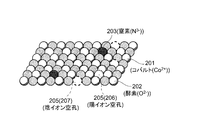
- FIG. 4 is a schematic perspective view illustrating the state of the electrode surface in the nonvolatile memory device according to the first embodiment of the invention. That is, this figure illustrates, as an example, the state of elements in the second layer 141b on the interface side of the first electrode 141 with the memory layer 142 when the first electrode 141 is cobalt oxide.
- the first electrode 141 is made of cobalt oxide. That is, the metallic element 201 is cobalt, and the first nonmetallic element 202 is oxygen.
- the second nonmetallic element 203 contains nitrogen.
- the second non-metallic element 203 having a valence 1 larger than that of the first non-metallic element 202 (oxygen) is formed in the second layer 141b of the first electrode 141.
- (Nitrogen) has been introduced.
- the lattice defects 205 in the second layer 141b correspond to metal elements compared to the number of second lattice defects (anion vacancies) 207 of anions corresponding to nonmetallic elements in order to maintain electrical neutrality.
- the number of first lattice defects (cation vacancies) 206 of the cation to be reduced is relatively reduced.
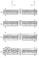
- FIG. 5 is a schematic cross-sectional view illustrating the operation in the nonvolatile memory device according to the first embodiment of the invention. That is, FIG. 5A illustrates an initial state of the storage unit 140 of the nonvolatile storage device 10, and FIG. 6B illustrates a state where the storage operation is repeated a predetermined number of times. (C) illustrates the state when the number of repetitions of the storage operation is larger than that in FIG.
- the first electrode 141 and the memory layer 142 are both made of oxide.
- a region doped with a group V element, that is, a second layer 141b is provided at the interface between the first electrode 141 and the memory layer 142.
- the first electrode 141 that repeats the storage operation of the nonvolatile storage device 10 and energizes the storage layer 142 by energizing the storage layer 142
- the first electrode The interface on the memory layer 142 side of 141 is oxidized, and the oxide layer 141p can be partially formed.
- the second layer 141b containing the second nonmetallic element is provided at the interface of the first electrode 141 on the memory layer 142 side.
- the number of the first lattice defects 206 of the cation corresponding to the metal element described with reference to FIG. 4 is relatively reduced, and the cobalt element is difficult to move, and thus is generated at the interface.
- the growth of the oxide layer 141p is suppressed. That is, the oxide layer 141p is prevented from proceeding into the first layer 141a, for example.
- the thickness of the oxide layer 141p generated by energization remains very thin.
- the thickness of the oxide layer 141p generated by energization is suppressed to about 1 nm or less. Thereby, the electrical characteristics of the storage unit 140 due to the partial formation of the oxide layer 141p do not change in practice.
- the oxide layer 141p has the first electrode 141, the storage layer 142, It can be formed on the entire surface of the interface.
- the thickness of the oxide layer 141p remains very thin.
- the thickness of the oxide layer 141p is also suppressed to about 1 nm or less.
- the first electrode 141 is oxidized with a large thickness by controlling lattice defects at the interface between the first electrode 141 and the memory layer 142. This can be suppressed. That is, according to the nonvolatile memory device 10, a nonvolatile memory device that suppresses deterioration of the electrode (first electrode 141) and has a long operation life is provided.
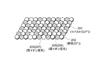
- FIG. 6 is a schematic perspective view illustrating the state of the electrode surface in the nonvolatile memory device of the comparative example. That is, this figure illustrates the state of elements in the second layer 141b on the interface side with the memory layer 142 of the first electrode 141 when the first electrode 141 is cobalt oxide.
- the second layer 141 b is not provided on the interface side of the first electrode 141 with the memory layer 142.
- the first electrode 141 in the nonvolatile memory device of the comparative example is made of cobalt oxide. That is, the metallic element 201 is cobalt, and the first nonmetallic element 202 is oxygen.
- a lattice defect 205 is formed in the cobalt oxide that becomes the first electrode 141.
- the defect of the metal element 201 cobalt
- the nonmetallic element 202 oxygen
- the second lattice defects 207 due to anion vacancies.
- five first lattice defects 206 that are cation vacancies and five second lattice defects 207 that are anion vacancies are formed in a predetermined area. Is done.
- many lattice defects are formed. Thereby, the first electrode 141 is easily oxidized.
- FIG. 7 is a schematic cross-sectional view illustrating the operation in the nonvolatile memory device of the comparative example. That is, FIG. 6A illustrates an initial state of the storage unit 140 of the nonvolatile storage device, and FIG. 6B illustrates a state where the storage operation is repeated a predetermined number of times. c) illustrates a state when the number of repetitions of the storage operation is larger than that in FIG.
- both the first electrode 141 and the memory layer 142 are made of oxide.
- the first electrode 141 that causes current to flow into the memory layer 142 is oxidized, and the memory layer 142 of the first electrode 141
- An oxide layer 141p is partially formed, for example, on the interface side.
- the metal element 201 included in the first electrode 141 is easily oxidized. If the metal element 201 is a material that is oxidized by oxygen contained in the memory layer 142, oxidation occurs without delivering electrons, and an oxide layer 141 p serving as a resistance layer is formed. Further, in the nonvolatile memory device, if Joule heat is generated even during resetting of current conduction, particularly when a large current flows, oxidation of the metal element is likely to occur.
- the oxide layer 141p increases in thickness, and is formed on the entire surface of the first electrode 141 on the memory layer 142 side.
- the thickness of the oxide layer 141p is 5 nm to 10 nm as a result of observation with a transmission electron microscope.
- the interface between the first electrode 141 and the memory layer 142 has a large influence such as poor conductivity.
- the operation of the storage unit 140 becomes unstable.
- a voltage is applied to the storage unit 140 in which such an oxide layer 141p is formed, current consumption due to the resistance of the oxide layer 141p is added and heat is also generated.
- the oxide layer 141p is formed thick, and this oxide layer 141p increases resistance and causes unstable operation. This causes heat generation and leads to shortening of the lifetime of the nonvolatile memory device itself.
- the number of first lattice defects 206 can be significantly reduced to 1/5 as compared with the nonvolatile memory device of the comparative example.
- the density of cobalt defects becomes low, cobalt becomes difficult to move, and the diffusion rate decreases.
- the first electrode 141 can be prevented from being oxidized with a large thickness at the interface between the first electrode 141 and the storage layer 142, and the electrode (first electrode 141) can be prevented.
- a nonvolatile memory device that suppresses deterioration and has a long operation life is provided.
- the thickness of the oxide layer 141p that can be formed on the first electrode 141 is less than half that of the comparative example due to the effect of the present embodiment. Then, the number of first lattice defects 206 due to metal element deficiency is extremely reduced. When the oxidation from the interface to the inner side of the first electrode 141 is extremely suppressed, the thickness of the oxide layer 141p is suppressed to about 1 nm, which is about 1/5 of the comparative example. Thus, the oxide layer 141p grows as the number of memory operations increases, and the thickness of the oxide layer 141p is a comparative example even when the oxide layer 141p covers the entire interface with the memory layer 142 of the first electrode 141. It is thinner than that, and good memory operation can be continued.
- the second non-metallic element 203 is included in the interface portion of the first electrode 141 on the memory layer 142 side. In the case where the second nonmetallic element 203 is contained over the thickness of the first electrode 141, it is not desirable because it adversely affects the electrical characteristics of the first electrode 141.
- the second electrode 141b containing the second non-metallic element is provided with a thin layer thickness at the interface of the first electrode 141 on the memory layer 142 side, and the first electrode
- the electrical characteristics of 141 are exhibited by the first layer 141a, and the thin second layer 141b is provided with a function of preventing oxidation of the first layer 141a.
- the oxidation of the first electrode 141 can be suppressed while maintaining the electrical characteristics of the first electrode 141.
- the first electrode 141 that conducts current from the electrode toward the memory layer 142 includes the metal element 201 and the first nonmetallic element 202 having the first valence n.
- the first electrode 141 that conducts current from the electrode toward the memory layer 142 includes the metal element 201 and the first nonmetallic element 202 having the first valence n. And a second non-metallic element 203 having a second valence (n + 1) larger than the first valence n in addition to the metal element 201 at the interface on the memory layer 142 side.
- the density of defects of the metal element 201 becomes low, the metal element (for example, cobalt) becomes difficult to move, and the diffusion rate decreases.
- the first valence n can be 2 and the second valence (n + 1) can be 3.
- the first nonmetallic element 202 is oxygen
- the second nonmetallic element 203 can include at least one selected from the group consisting of nitrogen, phosphorus, arsenic, and antimony. .
- the metal element 201 can be Co
- the first nonmetallic element 202 can be oxygen
- the second nonmetallic element 203 can be nitrogen or phosphorus. That is, the first electrode 141 is CoO 2 and contains nitrogen or phosphorus on the interface side with the memory layer 142.
- the metal element 201 can be W
- the first nonmetallic element 202 can be oxygen
- the second nonmetallic element 203 can be nitrogen or phosphorus. That is, the first electrode 141 is WO 3 and contains nitrogen or phosphorus on the interface side with the memory layer 142.
- the proportion of nitrogen in the second nonmetallic element 203 is 50 mole percent. This can be done. That is, by using more stable nitrogen among nitrogen, phosphorus, arsenic, and antimony, generation of the oxide layer 141p can be suppressed more stably.
- first valence n can be set to 3
- second valence (n + 1) can be set to 4.
- the first nonmetallic element 202 is nitrogen
- the second nonmetallic element 203 may include at least one selected from the group consisting of carbon, silicon, and germanium.
- the metal element 201 can be Ti
- the first nonmetallic element 202 can be nitrogen
- the second nonmetallic element 203 can be carbon. That is, the first electrode 141 is TiN and contains carbon on the interface side with the memory layer 142.
- the ratio of the second nonmetallic element 203 to the first nonmetallic element 202 is preferably 0.03 mole percent (mol%) to 10 mole percent (mol%).
- the ratio of the second nonmetallic element 203 to the first nonmetallic element 202 is lower than 0.03 mol%, the effect obtained by the nonvolatile memory device according to this embodiment described above is reduced.
- the ratio of the second nonmetallic element 203 to the first nonmetallic element 202 is higher than 10 mol%, it is easy to form a heterogeneous phase, leading to deterioration of electrical contact.
- the ratio of the second nonmetallic element 203 to the first nonmetallic element 202 is more preferably 0.5 mole percent to 10 mole percent.
- the thickness of the second layer 141b is preferably 0.1 nm or more and 10 nm or less.
- the thickness of the second layer 141b is thinner than 0.1 nm, the effect obtained by the nonvolatile memory device according to this embodiment described above is reduced.
- the thickness of the second layer 141b is larger than 10 nm, for example, the electric resistance of the second layer 141b is higher than that of the first layer 141a, and as a result, the resistance of the first electrode 141 is increased, which is not desirable. .
- the thickness of the second layer 141b is more preferably 1 nm or more and 5 nm or less.
- the metal element 201 includes at least one selected from the group consisting of Ti, Ta, Zr, Hf, W, Mo, Ni, Er, Mn, Nb, Co, Fe, Cu, Zn, and Sr. it can. That is, the first electrode 141 includes at least one selected from the group consisting of Ti, Ta, Zr, Hf, W, Mo, Ni, Er, Mn, Nb, Co, Fe, Cu, Zn, and Sr. Including.
- the memory layer 142 includes an oxide including at least one selected from the group consisting of Ti, Ta, Zr, Hf, W, Mo, Ni, Er, Mn, Ir, Nb, Sr, and Ce. be able to. Further, the memory layer 142 can include an oxide containing two or more metal elements.
- the film formation is performed.
- a method including a step of forming a film using a target mixed with a material to be a second nonmetallic element in the part can be used.
- nitride that becomes the second non-metallic element 203 is mixed in, for example, an oxide containing the metal element 201 and the second non-metallic element 202, and the target is sintered while maintaining uniformity as much as possible.
- a metal oxide doped with the second non-metallic element 203 can be obtained by forming a film of the material from the target by forming a plume with a laser or knocking it out by a sputtering method.
- the second non-metallic element 203 for example, a raw material of a nitrogen compound is separately prepared, and film formation is thereby performed. Formation of the layer 141b can be realized. At this time, the amount of the compound containing the metal element 201 and the first nonmetallic element (for example, an oxide compound) can be reduced in accordance with the increase in the compound containing the second nonmetallic element 203 (for example, a nitrogen compound).
- MOCVD Metal Organic Chemical Vapor Deposition
- the second non-metallic element 203 for example, nitride is dissolved in the coating solution within a range that does not cause precipitation in the raw material. It becomes possible.
- the MOCVD method for example, it is necessary to reduce the amount of oxygen compound corresponding to the increase in the amount of nitrogen compound, but this maintains the stoichiometry.
- This technique is also a technique that makes it easy to improve the compositional uniformity of the material because it is precipitated from the solution.
- the order of the formation of the first electrode 141 and the formation of the memory layer 142 is arbitrary as long as technically possible.
- the second layer 141b is formed after the formation of the first layer 141a of the first electrode 141.
- a method of forming a nitride thin film by physical vapor deposition can be used.
- the film thickness of the second layer 141b can be controlled by the film formation time and the film formation conditions.
- the total thickness of the second layer 141b is 10 nm or less, and a layer to be the memory layer 142 is formed thereon.
- the total thickness of the second layer 141b is set to 10 nm or less because the thermal history that the material to be the memory layer 142 receives during film formation (for example, about 500 ° C. for a total of 1 hour or 900 ° C. (Several seconds), based on the transmission electron microscope M observation results that the growth of other oxide-based oxide films is about 1 nm when the number is small and 10 nm when the number is large.
- the material that becomes the memory layer 142 is, for example, a temperature of 700 to 900 ° C. for several seconds when the diode that becomes the rectifying element portion 150 is activated. Receive history. As a result, the p-type semiconductor and the n-type semiconductor are interdiffused, and the configuration of the present embodiment is realized. At this time, a trace amount of a component of the second non-metallic element (for example, nitrogen) is also diffused into the interface of the memory layer 142 on the first electrode 141 side.
- a trace amount of a component of the second non-metallic element for example, nitrogen
- the first electrode 141 is formed after the memory layer 142 is formed
- various methods similar to the method described above can be used.
- the second layer 141b containing, for example, nitrogen, phosphorus, arsenic, and antimony that becomes the second nonmetallic element 203 is formed at a distance at which sufficient mutual diffusion can be expected due to the thermal history. That is, these non-metal layers that become the memory layer 142 are diffused.
- the second nonmetallic element 203 (for example, nitrogen, phosphorus, arsenic, antimony, etc.) is introduced into the interface of the first electrode 141 on the storage layer 142 side, and the first A non-metallic element 202 (for example, oxygen) is substituted. That is, for example, if nitrogen is introduced into a metal oxide, it enters a site where oxygen is present, so that lattice defects move to maintain electrical neutrality. In this case, when a new substance is not particularly added to the metal element, since nitrogen is trivalent and has a higher valence than oxygen divalent, a state where there are many defects on the side where oxygen mainly exists is realized. .
- the amount of lattice defects is determined by the material and temperature, but when the doped material is small, the total amount of lattice defects often does not change significantly. Therefore, in the state where nitrogen is slightly doped in the metal oxide, the number of lattice defects is almost the same as that before doping, and in addition, a lattice is used to maintain electrical neutrality on the side occupying oxygen and nitrogen which are non-metallic sites. There are many defects. Conversely, the number of metal site lattice defects, that is, the first lattice defect 206 is reduced.
- the metal element 201 of the first electrode 141 is densely present at the interface between the memory layer 142 and the first electrode 141. Therefore, even if oxidation occurs, the oxidation is limited to the metal element 201 existing in the vicinity of the boundary layer.
- the metal element 201 inside the first electrode 141 is likely to be oxidized due to defects in the metal element 201. In this case, the metal element 201 inside the first electrode 141 is oxidized. Contact resistance increases because volume expansion and the like can occur. In general, when a metal atom is oxidized, the molecular weight of the unit increases and the density decreases, so the volume often expands to about twice.
- the second nonmetallic element 203 is included in the interface between the memory layer 142 of the first electrode 141, thereby Oxidation of the one electrode 141 is suppressed, and it is possible to operate stably without increasing the interface resistance over a long period of operation.
- a second non-metallic element 203 (for example, carbon, silicon, germanium, or the like) is introduced into the interface of the first electrode 141 on the memory layer 142 side to replace the first non-metallic element 202 (for example, nitrogen). You may do it. Also in this case, the mechanism similar to the above can suppress the oxidation of the first electrode 141, and can operate stably without increasing the interface resistance over a long period of operation.
- the first electrode 141 it is preferable to use an oxide for the memory layer 142. If a material that is not an oxide is used as the memory layer 142, mutual diffusion or another compound may be formed between the oxide of the first electrode 141 and the stability may be impaired. . For this reason, it is desirable to use an oxide-based material for both the first electrode 141 on the side where current flows into the memory layer 142 and the memory layer 142.
- the nonvolatile memory device of the example according to the present embodiment will be described.
- the memory unit 140 including the memory layer 142 and the first electrode 141 is characterized, other components such as the first wiring 110, the second wiring 120, and the rectifying element are included. Description of the unit 150 is omitted.
- TiN is used for the first layer 141a of the first electrode 141, and a material containing nitrogen in TiO 2 is used for the second layer 141b.
- the metal element 201 is Ti
- the first nonmetallic element 202 is oxygen
- the second nonmetallic element 203 is nitrogen.
- the doping amount of nitrogen in the second layer 141b is changed.
- ZnMn 2 O 4 is used as the memory layer 142.
- TiO 2 powder and TiN powder in the molar ratio of nonmetallic elements of 0.010, 0.030, 0.10, 0.30, 1.0, 3.0, 5.0, 10, 20, 25, respectively. % And sintering to produce 2 inch diameter targets.
- a Si substrate provided with a TiN layer to be the first layer 141a of the first electrode 141 is placed in a vacuum chamber, and a film is formed by the PLD method using each of the targets 1Ta to 1Tj.
- the temperature of the Si substrate is 500 ° C.
- the laser light output is 130 mJ / mm 2 under oxygen conditions of 1 ⁇ 10 ⁇ 1 Pa.
- the film thickness to be formed is set to about 10 nm.
- a sample is obtained in which the second layer 141b in which oxygen (O) of TiO 2 is substituted with nitrogen (N) at various component ratios is formed on the TiN layer of the silicon substrate.
- the second layer 141b in which the metal element 201 is Ti, the first nonmetal element 202 is oxygen, and the second nonmetal element 203 is nitrogen is obtained.
- Samples obtained corresponding to the targets 1Ta, 1Tb, 1Tc, 1Td, 1Te, 1Tf, 1Tg, 1Thg, 1Ti, and 1Tj were used as samples 1Tab, 1Tbb, 1Tcb, 1Tdb, 1Teb, 1Tfb, 1Tgb, 1Thb, 1Tib. And 1Tjb.
- the content rate of the nitrogen which is the 2nd nonmetallic element 203 is changed.
- a target made of ZnMn 2 O 4 is used on the second layer 141b of each of the samples 1Tab, 1Tbb, 1Tcb, 1Tdb, 1Tb, 1Tfb, 1Tgb, 1Thb, 1Tib, and 1Tjb.
- a memory layer film is formed on the second layer 141b of each of the samples 1Tab, 1Tbb, 1Tcb, 1Tdb, 1Tb, 1Tfb, 1Tgb, 1Thb, 1Tib, and 1Tjb.
- the film thickness is set to about 20 nm by adjusting the film formation time.
- the film forming temperature is 400 ° C. and the oxygen partial pressure is 1 Pa.
- the samples corresponding to the samples 1Tab, 1Tbb, 1Tcb, 1Tdb, 1Tb, 1Tfb, 1Tgb, 1Thb, 1Tib and 1Tjb obtained in this way are respectively sample 1Tar, 1Tbr, 1Tcr, 1Tdr, 1Ter, 1Tfr, 1Tgr, 1Thr, 1Tir, and 1Tjr.
- samples 1Tar, 1Tbr, 1Tcr, 1Tdr, 1Ter, 1Tfr, 1Tgr, 1Thr, 1Tir and 1Tjr are set in a vacuum chamber, and a 50 ⁇ m diameter circle is formed on the memory layer film by sputtering using a mask. A columnar Pt pad is formed.
- the samples corresponding to the above samples 1Tar, 1Tbr, 1Tcr, 1Tdr, 1Ter, 1Tfr, 1Tgr, 1Thr, 1Tr, and 1Tjr obtained in this way are respectively sample 1Tas, 1Tbs, 1Tcs, 1Tds, 1Tes, 1Tfs, 1Tgs, Let 1Ths, 1Tis, and 1Tjs.
- the samples whose switching operation is no longer in the operation state after 10,000 times are samples 1Tas, 1Ths, 1Tis, and 1Tjs.
- the samples 1Tbs, 1Tcs, 1Tds, 1Tes, 1Tfs, and 1Tgs are confirmed to operate even when the number of switching is 50,000.
- the amount of nitrogen to be doped when the amount of nitrogen to be doped is 0.030 mol% to 10.0 mol%, there is an effect of increasing the number of times of switching. That is, the oxidation of the first electrode 141 is suppressed.
- the amount of nitrogen to be doped when the amount of nitrogen to be doped is less than 0.030 mol%, it is considered that the antioxidant power of the first electrode 141 is insufficient.
- TiN is used for the first layer 141a of the first electrode 141 and nitrogen is added to TiO 2 for the second layer 141b, as in the first embodiment.
- a material containing is used.
- ZnMnO 3 is used as the memory layer 142.
- the nitrogen doping amount in the second layer 141b can be changed.
- the TiN powder is mixed with the TiO 2 powder in a molar ratio of nonmetallic elements of 0.010, 0.030, 0.10, 0.30, 1.0, and 3. It is mixed and sintered at 0, 5.0, 10, 20, and 25% to obtain targets 2Ta, 2Tb, 2Tc, 2Td, 2Te, 2Tf, 2Tg, 2Th, 2Ti, and 2Tj, respectively.
- a Si substrate provided with a TiN layer to be the first layer 141a of the first electrode 141 is placed in a vacuum chamber, and a film is formed by the PLD method using the various targets described above. .
- the conditions at this time are the same as in the first embodiment.
- a sample is obtained in which the second layer 141b containing TiO 2 and TiN with various component ratios is formed on the TiN layer of the silicon substrate.
- Samples obtained corresponding to the respective targets used are designated as samples 2Tab, 2Tbb, 2Tcb, 2Tdb, 2Teb, 2Tfb, 2Tgb, 2Thb, 2Tib and 2Tjb.
- a storage layer film to be the storage layer 142 is formed by a PLD method using a target made of ZnMnO 3 .
- the conditions at this time are the same as in the first embodiment.
- the samples thus obtained are referred to as samples 2Tar, 2Tbr, 2Tcr, 2Tdr, 2Ter, 2Tfr, 2Tgr, 2Thr, 2Tir and 2Tjr, respectively.
- samples 2Tas, 2Tbs, 2Tcs, 2Tds, 2Tes, 2Tfs, 2Tgs, 2Ths, 2Tis and 2Tjs are referred to as samples 2Tas, 2Tbs, 2Tcs, 2Tds, 2Tes, 2Tfs, 2Tgs, 2Ths, 2Tis and 2Tjs, respectively.
- the samples whose switching operation is no longer in the operation state after 10,000 times are Samples 2Tas, 2Ths, 2Tis, and 2Tjs.
- the samples 2Tbs, 2Tcs, 2Tds, 2Tes, 2Tfs, and 2Tgs are confirmed to operate even when the number of switching is 50,000.
- the amount of nitrogen to be doped when the amount of nitrogen to be doped is 0.030 mol% to 10.0 mol%, there is an effect of increasing the number of times of switching. That is, the oxidation of the first electrode 141 is suppressed.
- the amount of nitrogen to be doped when the amount of nitrogen to be doped is less than 0.030 mol%, it is considered that the antioxidant power of the first electrode 141 is insufficient.
- TiN is used for the first layer 141a of the first electrode 141
- TiO 2 and nitrogen are used for the second layer 141b, as in the first embodiment.
- a material containing phosphorus and phosphorus is used.
- the nitrogen and phosphorus dope ratio can be changed.
- ZnMn 2 O 4 is used as in the first embodiment.
- a target in which nitrogen and phosphorus are doped at a total atomic percentage (atm%) in terms of oxygen ratio is prepared on a TiO 2 target.
- the nitrogen ratio with respect to the total amount of nitrogen and phosphorus is set to 10, 20, 30, 40, 50, 60, 70, 80, 90, and 100%.
- the target is 2 inches in diameter.
- targets having nitrogen ratios of 10, 20, 30, 40, 50, 60, 70, 80, 90, and 100% are converted into targets 3Ta, 3Tb, 3Tc, 3Td, 3Te, 3Tf, 3Tg, 3Th, and 3Ti, respectively.
- 3Tj targets having nitrogen ratios of 10, 20, 30, 40, 50, 60, 70, 80, 90, and 100% are converted into targets 3Ta, 3Tb, 3Tc, 3Td, 3Te, 3Tf, 3Tg, 3Th, and 3Ti, respectively.
- 3Tj is a target in which nitrogen and phosphorus are doped at a total atomic percentage (atm%)
- a film is formed on the Si substrate provided with the TiN layer to be the first layer 141a of the first electrode 141 by the PLD method using each of the targets 3Ta to 3Tj. To do.
- the conditions at this time are the same as in the first embodiment.
- a sample is obtained in which the second layer 141b containing TiO 2 , nitrogen, and phosphorus is formed in various component ratios on the TiN layer of the silicon substrate. That is, the second layer 141b is obtained in which the metal element 201 is Ti, the first nonmetallic element 202 is oxygen, and the second nonmetallic element 203 includes at least one of nitrogen and phosphorus.
- Samples obtained corresponding to the respective targets are designated as samples 3Tab, 3Tbb, 3Tcb, 3Tdb, 3Teb, 3Tfb, 3Tgb, 3Thb, 3Tib and 3Tjb.
- the content ratio of nitrogen and phosphorus in the second nonmetallic element 203 is changed.
- a memory layer film that becomes the memory layer 142 is formed by a PLD method using a target made of ZnMn 2 O 4 .
- the conditions at this time are the same as in the first embodiment.
- the samples thus obtained are referred to as samples 3Tar, 3Tbr, 3Tcr, 3Tdr, 3Ter, 3Tfr, 3Tgr, 3Thr, 3Tir and 3Tjr, respectively.
- a Pt pad is formed on each of the various samples as in the first embodiment.
- the samples thus obtained are referred to as Samples 3Tas, 3Tbs, 3Tcs, 3Tds, 3Tes, 3Tfs, 3Tgs, 3Ths, 3Tis and 3Tjs, respectively.
- the samples whose switching operation is no longer in the operation state after 10,000 times are samples 3Tfs, 3Tgs, 3Ths, 3Tis, and 3Tjs.
- the samples 3Tas, 3Tbs, 2Tcs, 2Tds, and 2Tes are confirmed to operate even when the number of switching is 80,000.
- the proportion of nitrogen in the second nonmetallic element 203 is 50 mole percent. This can be done. That is, by using more stable nitrogen among nitrogen, phosphorus, arsenic, and antimony, generation of the oxide layer 141p can be suppressed more stably.
- TiN is used for the first layer 141a of the first electrode 141 and CoO 2 and nitrogen are used for the second layer 141b, as in the first embodiment.
- a material containing is used. That is, in this example, the metal element 201 is Co, the first nonmetallic element 202 is oxygen, and the second nonmetallic element 203 is nitrogen.
- ZnMn 2 O 4 is used as in the first embodiment. Then, the film thickness of the memory layer 142 is changed.
- a target obtained by doping CoO 2 target with nitrogen at 1.0 atm% in terms of oxygen ratio is prepared.
- a film is formed on the Si substrate provided with the TiN layer to be the first layer 141a of the first electrode 141 by the PLD method using the above target.
- the conditions at this time are the same as in the first embodiment.
- a sample is obtained in which the second layer 141b containing CoO 2 and nitrogen is formed on the TiN layer of the silicon substrate. And let the obtained sample be the sample 4 Tab.
- a storage layer film to be the storage layer 142 is formed by a PLD method using a target made of ZnMn 2 O 4 .
- the film thickness is adjusted to 5, 10, 15, 20, 25, 30, 40, 50, 75, and 100 nm by adjusting the film formation time.
- the film forming temperature is 400 ° C. and the oxygen partial pressure is 1 Pa.
- Samples corresponding to the film thicknesses of 5, 10, 15, 20, 25, 30, 40, 50, 75, and 100 nm obtained in this manner were respectively obtained as samples 4Tar, 4Tbr, 4Tcr, 4Tdr, 4Ter, 4Tfr, 4Tgr, 4Thr, 4Tir, and 4Tjr.
- a Pt pad is formed on each of the various samples as in the first embodiment.
- the samples thus obtained are referred to as Samples 3Tas, 3Tbs, 3Tcs, 3Tds, 3Tes, 3Tfs, 3Tgs, 3Ths, 3Tis and 3Tjs, respectively.
- the switching frequency in this case is 50,000 times.
- the sample 4Tas is the only sample that is not in the operating state after switching operation is 10,000 times or less. That is, the operating state of the samples 3Tbs, 3Tcs, 3Tds, 3Tes, 3Tfs, 3Tgs, 3Ths, 3Tis, and 3Tjs is confirmed even when the number of switching is 50,000 times.
- the second layer 141b of the first electrode 141 is a Co-based electrode
- the effect of preventing oxidation is exhibited by doping with nitrogen.
- the number of times of switching is small due to a short circuit between the electrodes.
- the oxidation of the first electrode 141 proceeds. Can be suppressed.
- the TiN powder is mixed with the TiO 2 powder in a molar ratio of nonmetallic elements of 0.010, 0.030, 0.10, 0.30, 1.0, and 3. It is mixed and sintered at 0, 5.0, 10, 20, 25% to obtain targets 5Ta, 5Tb, 5Tc, 5Td, 5Te, 5Tf, 5Tg, 5Th, 5Ti, and 5Tj, respectively.
- a Si substrate provided with a TiN layer to be the first layer 141a of the first electrode 141 is placed in a vacuum chamber, and a film is formed by the PLD method using the various targets described above. .
- the conditions at this time are the same as in the first embodiment.
- a sample is obtained in which the second layer 141b containing TiO 2 and TiN with various component ratios is formed on the TiN layer of the silicon substrate.
- Samples obtained corresponding to the respective targets used are referred to as samples 5Tab, 5Tbb, 5Tcb, 5Tdb, 5Teb, 5Tfb, 5Tgb, 5Thb, 5Tib, and 5Tjb.
- a storage layer film to be the storage layer 142 is formed by a PLD method using a target made of Pr 2 CaMn 3 O 6 .
- the conditions at this time are the same as in the first embodiment.
- the film forming temperature is 700 ° C.
- the samples thus obtained are referred to as samples 5Tar, 5Tbr, 5Tcr, 5Tdr, 5Tr, 5Tfr, 5Tgr, 5Thr, 5Tir, and 5Tjr, respectively.
- samples 5Tas, 5Tbs, 5Tcs, 5Tds, 5Tes, 5Tfs, 5Tgs, 5Ths, 5Tis and 5Tjs are referred to as samples 5Tas, 5Tbs, 5Tcs, 5Tds, 5Tes, 5Tfs, 5Tgs, 5Ths, 5Tis and 5Tjs, respectively.
- the samples whose switching operation is no longer in the operation state after 10,000 times are samples 5Tas, 5Ths, 5Tis, and 5Tjs.
- the sample 5Tbs, 5Tcs, 5Tds, 5Tes, 5Tfs, and 5Tgs are confirmed to operate even when the number of switching is 50,000.
- Example 1 when the amount of nitrogen to be doped is 0.030 mol% to 10.0 mol%, there is an effect of increasing the number of switching operations. That is, the oxidation of the first electrode 141 is suppressed. On the other hand, when the amount of nitrogen to be doped is less than 0.030 mol%, it is considered that the antioxidant power of the first electrode 141 is insufficient.
- a perovskite oxide having a relatively high deposition temperature is used as the material used for the memory layer 142. In this case, the first electrode 141 similar to the first embodiment is used. An antioxidant effect is obtained.
- FIG. 8 is a flowchart illustrating the method for manufacturing the nonvolatile memory device according to the second embodiment of the invention.
- the stacked structure 145 including the memory layer 142 and an electrode (first electrode 141) that flows current toward the memory layer 142, and the voltage applied to the memory layer 142.
- a voltage application unit 101 for storing information by causing a resistance change in the memory layer 142 by applying a current to the memory layer 142 and manufacturing the nonvolatile memory device.
- the voltage application unit 101 can include, for example, a bit wiring (BL) that is the first wiring 110 and a word line (WL) that is the second wiring 120.
- BL bit wiring
- WL word line
- the metal element 201 that becomes a part of the electrode (first electrode 141) and the first valence n are set.
- a first layer film 141af having the first nonmetallic element 202 is formed (step S110).
- the metal element 201 and the first valence n of the first nonmetal element 202 which are another part of the electrode (first electrode 141) and become the second layer 141b on the memory layer 142 side.
- a second layer film 141bf having a second non-metallic element 203 having a second valence (n + 1) larger than 1 is formed (step S120).
- the second layer film 141bf may further contain the first non-metallic element 202.
- the second nonmetallic element 203 having a valence 1 larger than that of the first nonmetallic element 202 can be included on the interface side of the memory layer 142 of the first electrode 141, and the electrode (first electrode 141)
- a method of manufacturing a nonvolatile memory device that suppresses deterioration and has a long operation life is provided.
- step S120 a film to be the memory layer 142 is formed.
- the order of step S110 and step S120 can be interchanged, and after step S120 for forming the second layer film 141bf to be the second layer 141b, the first layer 141a to be the first layer 141a of the first electrode 141 is formed.
- Step S110 for forming the single-layer film 141af may be performed. In this case, a film that becomes the memory layer 142 is formed before step S120.
- Step S110, Step S120, and the formation of the film that becomes the memory layer 142 for example, various films that become the rectifying element unit 150, films that become the first wiring 110, and second wiring A film to be 120 can be formed.
- the stacked structure 145 including the first electrode 141 and the memory layer 142 is sandwiched between the first and second wirings 110 and 120.
- a case where the manufacturing method is a cross-point type nonvolatile memory device will be described.
- FIG. 9 is a schematic cross-sectional view in order of the processes, illustrating the method for manufacturing the nonvolatile memory device according to the second embodiment of the invention.
- FIG. 10 is a schematic cross-sectional view in order of the processes following FIG. 9 and 10, the left side is a cross-sectional view parallel to the Y axis (cross-sectional view taken along the line AA ′ in FIG. 2), and the right side is a cross-sectional view parallel to the X axis (B-- in FIG. 2). B 'line sectional view).
- a film (first conductive film 110f) to be the first wiring 110 is formed on the substrate 105 made of silicon, and the second electrode 143 is formed thereon.
- a second electrode film 143f is formed, a memory layer film 142f to be the memory layer 142 is further formed thereon, and a second layer film 141bf to be the second layer 141b is further formed thereon.
- the first wiring 110 and the second electrode 143 can be used together, and in this case, the first conductive film 110f or the second electrode film 143f can be omitted.
- the first conductive film 110f imparts conductivity to at least the surface of the first wiring 110.
- Ti, Ta, Zr, Hf, W, Mo, W, Ni, Pt, Er, Ni, Ir At least one selected from the group consisting of Ru, Au, Nb, Sr, Si, Ga, and As can be used. Furthermore, an alloy containing at least two selected from this group can be used.
- the second layer film 141bf includes a metal element 201 and a second non-metal element 203.
- the second nonmetallic element 203 has a second valence (n + 1) that is one greater than the first valence n of the first nonmetallic element 202.
- the second layer film 141bf may further contain the first non-metallic element 202.
- the second layer film 141bf can be formed by various methods such as the PLD method, the MOCVD method, and the MOD method described above.
- the process illustrated in FIG. 9A corresponds to step S120 illustrated in FIG.
- a first layer film 141af to be the first layer 141a is formed on the second layer film 141bf.
- the metal element 201 includes at least one selected from the group consisting of Ti, Ta, Zr, Hf, W, Mo, Ni, Er, Mn, Nb, Co, Fe, Cu, Zn, and Sr. Can do.
- the first nonmetallic element for example, oxygen or nitrogen can be used.
- the first nonmetallic element 202 has a first valence n.
- step S110 illustrated in FIG. 9 is an example in which steps S110 and S120 illustrated in FIG. 8 are performed in the reverse order.
- the first layer film 141af can be formed by various methods such as the PLD method, the MOCVD method, and the MOD method described above.
- the first layer film 141af is formed on the memory layer film 142f, and then the second non-metallic element 203 included in the memory layer film 142f is diffused into the first layer film 141af, whereby the second layer film 141f is diffused.
- the layer film 141bf can also be formed.
- the second layer film 141bf is formed not by the film deposition method but by the diffusion method of the second non-metallic element 203.
- FIG. 9A a case where the second layer film 141 bf is formed by film deposition will be described.
- a rectifying element portion film 150f to be the rectifying element portion 150 is formed.
- the first conductive film 110f, the second electrode film 143f, the memory layer film 142f, the second layer film 141bf, the first layer film 141af, and the rectifying element portion film 150f are continuously formed. be able to.
- the rectifying element portion film 150f the first layer film 141af, the second layer film 141bf, the memory layer film 142f, the second electrode film 143f, and the first conductive film 110f.
- patterning is performed using photolithography and dry etching, and a film (insulating part film 160f) to be the insulating part 160 is formed (formed) by CVD (Chemical Vapor Deposition) or a coating method.
- the surface is flattened by CMP (Chemical Mechanical Polishing) method.
- the first wiring 110 is patterned so as to extend in a direction parallel to the X axis.
- a film for the second wiring 120 (second conductive film 120f) is formed by sputtering or CVD, and the first film is formed by, for example, photolithography and dry etching.
- the second conductive film 120f, the rectifying element part film 150f, the first layer film 141af, the second layer film 141bf, the memory layer film 142f, the second electrode film 143f, and the insulating part film 160f are patterned.
- tungsten, tungsten silicide, tungsten nitride, or the like can be used as the material of the second wiring 120, for example.
- these films are patterned so as to be orthogonal to the patterning direction of the first wiring 110, that is, so that the second wiring 120 extends in the Y-axis direction.
- a SiO 2 film is formed as a film to be the insulating part 160 so as to embed the space between the memory part 140 and the like by a CVD method or a coating method. Accordingly, the surface is flattened by the CMP method. Thereby, the nonvolatile memory device 10 having the single memory layer 142 illustrated in FIGS. 1 to 3 can be formed.
- a nonvolatile memory device having a multilayer memory unit 140 can be formed.
- a film for the second wiring 120 (second conductive film 120 f) is formed to form a memory portion including the first memory layer 142, and then a second rectifier element
- the partial film 150f, the first layer film 141af, the second layer film 141bf, the memory layer film 142f, and the second electrode film 143f are formed, the second conductive film 120f for the second wiring 120 of the first layer, the rectifying element Simultaneously with the patterning of the part film 150f, the first layer film 141af, the second layer film 141bf film, the memory layer film 142f, the second electrode film 143f, and the insulating part film 160f, the second rectifier element part film 150f, 1-layer film 141af, first Layer film 141Bf, storage layer film 142f, and the second electrode layer 143 f, can also be the second wiring 120 is patterned so as to extend in the Y-axis direction. Thereby, a process can be omitted. Furthermore, this
- the manufacturing method of the nonvolatile memory device provides the manufacturing method of the nonvolatile memory device that suppresses the deterioration of the electrode (first electrode 141) and has a long operation life.
- the third embodiment is a probe memory type nonvolatile memory device.
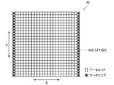
- 11 and 12 are a schematic perspective view and a schematic plan view illustrating the configuration of the nonvolatile memory device according to the third embodiment of the invention.
- the storage unit 522 provided on the conductive layer 521 is disposed on the XY scanner 516.
- the probe array is arranged so as to face the storage unit 522.
- the probe array includes a substrate 523 and a plurality of probes (heads) 524 arranged in an array on one surface side of the substrate 523.
- Each of the plurality of probes 524 is composed of a cantilever, for example, and is driven by multiplex drivers 525 and 526.
- Each of the plurality of probes 524 can be individually operated using the microactuator in the substrate 523. However, all the probes can be collectively operated to access the data area of the storage medium.
- all the probes 524 are reciprocated in the X direction at a constant cycle, and the position information in the Y direction is read from the servo area of the storage medium.
- the position information in the Y direction is transferred to the driver 515.
- the driver 515 drives the XY scanner 516 based on this position information, moves the storage medium in the Y direction, and positions the storage medium and the probe.
- data reading or writing is performed simultaneously and continuously on all the probes 524 on the data area.
- Data reading and writing are continuously performed because the probe 524 reciprocates in the X direction.
- Data reading and writing are performed on the data area line by line by sequentially changing the position of the storage unit 522 in the Y direction.
- the storage unit 522 may be reciprocated in the X direction at a constant period to read position information from the storage medium, and the probe 524 may be moved in the Y direction.
- the storage unit 522 is provided over the conductive layer 521 provided on the substrate 520, for example.
- the storage unit 522 has a plurality of data areas and servo areas arranged at both ends in the X direction of the plurality of data areas.
- the plurality of data areas occupy the main part of the storage unit 522.
- Servo burst signal is stored in the servo area.
- the servo burst signal indicates position information in the Y direction within the data area.
- the storage unit 522 further includes an address area for storing address data and a preamble area for synchronization.
- the data and servo burst signal are stored in the storage unit 522 as storage bits (electrical resistance fluctuation).
- the “1” and “0” information of the storage bit is read by detecting the electrical resistance of the storage unit 522.
- one probe is provided corresponding to one data area, and one probe is provided for one servo area.
- the data area is composed of a plurality of tracks.
- a track in the data area is specified by an address signal read from the address area.
- the servo burst signal read from the servo area is used to move the probe 524 to the center of the track and eliminate the storage bit reading error.
- the X direction correspond to the down-track direction
- the Y direction correspond to the track direction, it becomes possible to use the head position control technology of the HDD.
- the memory unit 522 has a stacked structure including an electrode (first electrode 141 not shown) and a memory layer (not shown).
- a voltage application unit is provided that applies a voltage to the storage layer and causes a current to flow to cause a resistance change in the storage layer to store information.
- the voltage application units are the conductive layer 521 and the probe 524. Note that in the above, the conductive layer 521 and the electrode of the memory portion 522 (first electrode 141) may be combined.
- storage part 522 supplies an electric current toward the said memory
- the electrode is provided between the first layer 141a including the metal element 201 and the first nonmetallic element 202 having the first valence n, and between the first layer 141a and the memory layer 142, and the metal A second layer 141b including an element 201, a first nonmetallic element 202, and a second nonmetallic element 203 having a second valence (n + 1) that is one greater than the first valence n.
- a combination of the metal element 201, the first non-metal element 202, and the second non-metal element 203 is applicable as in the first embodiment.
- the second layer 141b and the like can be implemented in the same manner as in the first embodiment.
- the method for manufacturing the nonvolatile memory device according to the second embodiment already described can be applied to the probe memory type nonvolatile memory device 30 according to this embodiment.
- a nonvolatile memory device that suppresses electrode deterioration and has a long operating life and a method for manufacturing the same are provided.
Landscapes
- Engineering & Computer Science (AREA)
- Chemical & Material Sciences (AREA)
- Nanotechnology (AREA)
- Materials Engineering (AREA)
- Physics & Mathematics (AREA)
- Mathematical Physics (AREA)
- Theoretical Computer Science (AREA)
- Crystallography & Structural Chemistry (AREA)
- Semiconductor Memories (AREA)
Abstract
電極と、前記電極に接続され、前記電極から流される電流により抵抗が変化する記憶層と、を備え、前記電極は、金属元素と、第1価数nを有する第1非金属元素と、を含む第1層と、前記第1層と前記記憶層との間に設けられ、前記金属元素と、前記第1価数nよりも1大きい第2価数(n+1)を有する第2非金属元素と、を含む第2層と、を有することを特徴とする不揮発性記憶装置が提供される。
Description
本発明は、不揮発性記憶装置及びその製造方法に関する。
近年、小型の携帯機器が世界的に普及すると同時に、高速情報伝送網の大幅な進展がみられ、小型大容量不揮発性メモリの需要が急速に拡大してきている。その中で、NAND型フラッシュメモリ及び小型HDD(hard disk drive)は、特に、急速な記録密度の進化を遂げ、携帯音楽市場や携帯ゲーム記録用メモリ、パソコンの記憶装置等、さまざまな用途に用いられている。しかしながら、これらの不揮発性メモリは、高密度化の限界があると言われている。
これに対し、次の不揮発性記憶装置として、相変化を利用するもの、磁気変化を用いるもの、強誘電体を利用するもの、抵抗変化を利用いるものなど、さまざまなメモリが提案されている。このなかで、抵抗変化型のメモリ、いわゆるReRAM(Resistive Random Access Memory)は、微細加工により消費電力が低減し、書き込み読み出し速度が従来よりも大幅に改善できるとして、期待が大きい。
このReRAMにおいては、記憶層となる抵抗変化型材料に電流を通電するための電極が設けられる。この時、ReRAMの動作中に、記憶層に電流が流れ込む側の電極が酸化され、この電極の特に記憶層に接する界面に高抵抗層が形成されることが懸念される。この高抵抗層は、ReRAMの動作を不安定にし、また、消費電力が増大させる他、例えば、大電流が通電されるリセット時に発生するジュール熱を大きくし、さらなる酸化を引き起こし、ReRAMの寿命を縮めてしまう。
一方、上記の電極として、酸化されにくい例えばPtなどの貴金属を用いることも考えられるが、高コストであり、また、加工性の点で実用性が低い。すなわち、上記の電極には、例えば金属酸化物などの金属化合物を用いることが望ましい。
従って、安価で加工性の高い金属化合物を用い、電極の劣化を抑制する技術が強く望まれている。
なお、特許文献1に、電気信号により抵抗が変化する金属酸化物層に接する電極として、TiNやZnOなどの窒化物や酸化物を用いる技術が開示されている。
特開2007-42784号公報
本発明は、電極の劣化を抑制し、動作寿命の長い不揮発性記憶装置及びその製造方法を提供する。
本発明の一態様によれば、電極と、前記電極に接続され、前記電極から流される電流により抵抗が変化する記憶層と、を備え、前記電極は、金属元素と、第1価数nを有する第1非金属元素と、を含む第1層と、前記第1層と前記記憶層との間に設けられ、前記金属元素と、前記第1価数nよりも1大きい第2価数(n+1)を有する第2非金属元素と、を含む第2層と、を有することを特徴とする不揮発性記憶装置が提供される。
また、本発明の他の一態様によれば、電極と、前記電極から流される電流により抵抗が変化する記憶層と、を有する積層構造体を有する不揮発性記憶装置の製造方法であって、前記電極の一部となる、金属元素と、第1価数nを有する第1非金属元素と、を有する第1層膜を形成する工程と、前記電極の別の一部であり前記記憶層の側の第2層となる、前記金属元素と、前記第1価数nよりも1大きい第2価数(n+1)を有する第2非金属元素と、を有する第2層膜を形成する工程と、を備えたことを特徴とする不揮発性記憶装置の製造方法が提供される。
10、20、21、30 不揮発性記憶装置
101 電圧印加部
105 基板
110 第1の配線
110f 第1の導電膜
120 第2の配線
120f 第2の導電膜
130 交差部
140 記憶部
141 第1電極
141a 第1層
141af 第1層膜
141b 第2層
141bf 第2層膜
141p 酸化層
142 記憶層
142f 記憶層膜
143 第2電極
143f 第2電極膜
145 積層構造体
150 整流素子部
150f 整流素子部膜
160 絶縁部
160f 絶縁部膜
201 金属元素
202 第1非金属元素
203 第2非金属元素
205 格子欠陥
206 第1格子欠陥(陽イオン空孔)
207 第2格子欠陥(陰イオン空孔)
515 ドライバ
516 XYスキャナ
520、523 基板
521 導電層
522 記憶部
524 プローブ
525、526 マルチプレクスドライバ
101 電圧印加部
105 基板
110 第1の配線
110f 第1の導電膜
120 第2の配線
120f 第2の導電膜
130 交差部
140 記憶部
141 第1電極
141a 第1層
141af 第1層膜
141b 第2層
141bf 第2層膜
141p 酸化層
142 記憶層
142f 記憶層膜
143 第2電極
143f 第2電極膜
145 積層構造体
150 整流素子部
150f 整流素子部膜
160 絶縁部
160f 絶縁部膜
201 金属元素
202 第1非金属元素
203 第2非金属元素
205 格子欠陥
206 第1格子欠陥(陽イオン空孔)
207 第2格子欠陥(陰イオン空孔)
515 ドライバ
516 XYスキャナ
520、523 基板
521 導電層
522 記憶部
524 プローブ
525、526 マルチプレクスドライバ
以下、本発明の実施の形態について図面を参照して詳細に説明する。
なお、図面は模式的または概念的なものであり、各部分の厚みと幅との関係、部分間の大きさの比率などは、必ずしも現実のものと同一とは限らない。また、同じ部分を表す場合であっても、図面により互いの寸法や比率が異なって表される場合もある。
なお、本願明細書と各図において、既出の図に関して前述したものと同様の要素には同一の符号を付して詳細な説明は適宜省略する。
なお、図面は模式的または概念的なものであり、各部分の厚みと幅との関係、部分間の大きさの比率などは、必ずしも現実のものと同一とは限らない。また、同じ部分を表す場合であっても、図面により互いの寸法や比率が異なって表される場合もある。
なお、本願明細書と各図において、既出の図に関して前述したものと同様の要素には同一の符号を付して詳細な説明は適宜省略する。
(第1の実施の形態)
図1は、本発明の第1の実施形態に係る不揮発性記憶装置の構成を例示する模式図である。
すなわち、同図(a)は要部の模式的斜視図、同図(b)は同図(c)のA-A’線断面図、同図(c)は同図(b)のB-B’線断面図である。
図2は、本発明の第1の実施形態に係る不揮発性記憶装置の構成を例示する模式図である。
すなわち、同図(a)は模式的斜視図、同図(b)は平面図である。
図3は、本発明の第1の実施形態に係る別の不揮発性記憶装置の構成を例示する模式的斜視図である。
図1は、本発明の第1の実施形態に係る不揮発性記憶装置の構成を例示する模式図である。
すなわち、同図(a)は要部の模式的斜視図、同図(b)は同図(c)のA-A’線断面図、同図(c)は同図(b)のB-B’線断面図である。
図2は、本発明の第1の実施形態に係る不揮発性記憶装置の構成を例示する模式図である。
すなわち、同図(a)は模式的斜視図、同図(b)は平面図である。
図3は、本発明の第1の実施形態に係る別の不揮発性記憶装置の構成を例示する模式的斜視図である。
第1の実施形態に係る不揮発性記憶装置はクロスポイント型の不揮発性記憶装置である。
まず、図1及び図2により、本実施形態の不揮発性記憶装置の構成の概要を説明する。 図2(a)、(b)に表したように、本発明の第1の実施形態に係る不揮発性記憶装置10においては、基板105の主面の上に、X軸方向に延在する帯状の第1の配線110が設けられている。そして、基板105に平行な面内でX軸と直交するY軸方向に延在する帯状の第2の配線120が、第1の配線110に対向して設けられている。
なお、上記では、第1の配線110と第2の配線120が直交する例であるが、第1の配線110と第2の配線120とは交差(非平行)であれば良い。
なお、このように、基板105の主面に対して並行な平面をX-Y平面とし、第1の配線110の延在する方向をX軸とし、X-Y平面内においてX軸と直交する軸をY軸とし、X軸及びY軸に対して垂直方向をZ軸とする。
まず、図1及び図2により、本実施形態の不揮発性記憶装置の構成の概要を説明する。 図2(a)、(b)に表したように、本発明の第1の実施形態に係る不揮発性記憶装置10においては、基板105の主面の上に、X軸方向に延在する帯状の第1の配線110が設けられている。そして、基板105に平行な面内でX軸と直交するY軸方向に延在する帯状の第2の配線120が、第1の配線110に対向して設けられている。
なお、上記では、第1の配線110と第2の配線120が直交する例であるが、第1の配線110と第2の配線120とは交差(非平行)であれば良い。
なお、このように、基板105の主面に対して並行な平面をX-Y平面とし、第1の配線110の延在する方向をX軸とし、X-Y平面内においてX軸と直交する軸をY軸とし、X軸及びY軸に対して垂直方向をZ軸とする。
なお、図2(a)、(b)においては、第1の配線110と第2の配線120とは、それぞれ4本ずつ設けられている例が示されているが、これには限らず、第1の配線110と第2の配線120の数は任意である。そして、例えば、第1の配線110がビット配線(BL)となり、第2の配線120がワード線(WL)となる。ただし、この場合、第1の配線110をワード線(WL)、第2の配線120をビット線(BL)としても良い。以下では、第1の配線110がビット配線(BL)であり、第2の配線120がワード線(WL)であるとして説明する。
そして、第1の配線110と第2の配線120の間に記憶部140が挟まれている。すなわち、不揮発性記憶装置10では、ビット配線とワード配線が3次元的に交差して形成される交差部130(クロスポイント)に記憶部140が設けられている。
図1に表したように、記憶部140は、第1電極(電極)141と、第2電極143と、第1電極141と第2電極143との間に設けられた記憶層142を有する積層構造体145を有する。
記憶層142には、例えば、電圧を印加して電流が流れると電気抵抗値が変化する、酸化ニッケル(NiOx)、酸化チタン(TiOx)、ZnMn2O4、PrxCa1-xMnO3等を用いることができる。さらに、記憶層142には、Ti、Ta、Zr、Hf、W、Mo、Ni、Er、Mn、Ir、Nb、Sr、及び、Ceよりなる群から選ばれた少なくとも1つを含む酸化物を含むことができる。ただし、本発明はこれに限らず、記憶層142には、電圧を印加して電流が流れると抵抗変化を示す全ての材料を用いることができる。
そして、第1の配線110に与える電位と第2の配線120に与える電位の組み合わせによって、各記憶部140(各積層構造体145)に印加される電圧が変化し、その時の記憶部140の特性によって、情報を記憶することができる。
この時、記憶部140に印加される電圧の極性に方向性を持たせるために、例えば整流特性を有する整流素子部150を設けることができる。整流素子部150には、例えば、PINダイオードやMIM(Metal-Insulator-Metal)素子などを用いることができる。なお、整流素子部150は、第1の配線110と第2の配線120とが対向する領域以外の領域に設けても良い。
なお、第1配線110と第2配線120との間に、記憶部140(積層構造体145)及び整流素子部150を設ける場合において、記憶部140及び整流素子部150の積層順は任意である。そして、後述するように、第1配線110、記憶部140、整流素子部150及び第2配線120からなる積層構造が、さらに複数設けられる場合において、記憶部140及び整流素子部150の積層順は任意であり、例えば、それぞれの積層構造において、記憶部140及び整流素子部150の積層順を同一にしても良く、また、変えても良い。
なお、第1配線110と第2配線120との間に、記憶部140(積層構造体145)及び整流素子部150を設ける場合において、記憶部140及び整流素子部150の積層順は任意である。そして、後述するように、第1配線110、記憶部140、整流素子部150及び第2配線120からなる積層構造が、さらに複数設けられる場合において、記憶部140及び整流素子部150の積層順は任意であり、例えば、それぞれの積層構造において、記憶部140及び整流素子部150の積層順を同一にしても良く、また、変えても良い。
基板105には、例えばシリコン基板を用いることができ、不揮発性記憶装置を駆動する駆動回路を設けることもできる。
第1の配線110及び第2の配線120には、金属元素を含む各種の導電性材料を用いることができる。
第1の配線110及び第2の配線120には、金属元素を含む各種の導電性材料を用いることができる。
なお、図1(a)及び図2(b)に表したように、第1の配線110と第2の配線120とが、3次元的に交差して形成される両者間の領域に、記憶部140は設けられ、この1つの記憶部140が1つの要素であり、セルと言う。
また、図1(b)、(c)に表したように、第1の配線110と、第2の配線120と、記憶部140は、間隔を置いて設けられた複数の領域を有しており、その複数の領域に挟まれるように、絶縁部160が設けられている。なお、図1(a)及び、図2(a)、(b)においては、絶縁部160は省略されて描かれている。
これら、絶縁部160には、例えば、電気抵抗の高い酸化珪素(SiO2)等を用いることができる。ただし、これに限らず、絶縁部160には、記憶部140の電気抵抗より高い各種の材料を用いることができる。
これら、絶縁部160には、例えば、電気抵抗の高い酸化珪素(SiO2)等を用いることができる。ただし、これに限らず、絶縁部160には、記憶部140の電気抵抗より高い各種の材料を用いることができる。
なお、上記において、第1電極141及び第2電極143の少なくともいずれかは、第1配線110及び第2配線120のいずれかで兼用されても良い。また、第1電極141及び第2電極143の少なくともいずれかは、整流素子部150となる導電層の例えば一部で兼用されても良い。
上記のように、本実施形態に係る不揮発性記憶装置10は、電極(第1電極141)と記憶層142とを有する積層構造体145と、記憶層142に電圧を印加し電流を流して記憶層142に抵抗変化を生じさせて情報を記憶させる電圧印加部101(すなわち、第1配線110及び第2配線120)と、を備える。
なお、以上の図1及び図2においては、第1の配線110、第2の配線120及びその間の記憶部140が積層された1層の積層構造体のみを例示しているが、この積層構造体を多数積層することで、高密度の記憶装置が構成できる。
すなわち、本実施形態に係る不揮発性記憶装置は、図3(a)に例示した不揮発性記憶装置20のような2層の積層構造体、図3(b)に例示した不揮発性記憶装置21のような4層構造の他、それ以上の数の層構造を有することができる。以下では、本実施形態に係る不揮発性記憶装置として、図1及び図2に例示した不揮発性記憶装置10を例に挙げて説明する。
すなわち、本実施形態に係る不揮発性記憶装置は、図3(a)に例示した不揮発性記憶装置20のような2層の積層構造体、図3(b)に例示した不揮発性記憶装置21のような4層構造の他、それ以上の数の層構造を有することができる。以下では、本実施形態に係る不揮発性記憶装置として、図1及び図2に例示した不揮発性記憶装置10を例に挙げて説明する。
本実施形態に係る不揮発性記憶装置10においては、第1電極(電極)141から第2電極143に向けて電流が通電されるものとする。すなわち、第1電極141は、第1電極141から記憶層142に向けて電流を通電する。
そして、本実施形態に係る不揮発性記憶装置10においては、第1電極141は、第1層141aと、第1層141aと記憶層142との間に設けられた第2層141bとを有する。
第1電極141は、金属元素と、第1価数nを有する第1非金属元素と、を含む。
そして、第1電極141は、記憶層142との界面に設けられた第2層141bを有し、第2層141bは、金属元素と、第1非金属元素よりも価数(の絶対値)が1つ大きい第2非金属元素と、を含んでいる。なお、第2層141bは、金属元素及び第2非金属元素に加え、上記の第1非金属元素を含んでも良い。
そして、第1電極141は、記憶層142との界面に設けられた第2層141bを有し、第2層141bは、金属元素と、第1非金属元素よりも価数(の絶対値)が1つ大きい第2非金属元素と、を含んでいる。なお、第2層141bは、金属元素及び第2非金属元素に加え、上記の第1非金属元素を含んでも良い。
すなわち、第2層141bにおいては、金属元素及び第1非金属元素からなる化合物において、例えば、第1非金属元素の少なくとも一部が第2非金属元素に置換されている。なお、本発明は、これに限らず、第1電極141の記憶層142との界面側に、第1非金属元素よりも価数(の絶対値)が1つ大きい第2非金属元素を含めば良い。
これにより、第1電極141の酸化の進行を防止し、電極(第1電極141)の劣化を抑制し、動作寿命の長い不揮発性記憶装置が提供される。
以下、一例として、上記の第1非金属元素が酸素である場合として説明する。
すなわち、第1電極141が、金属酸化物または金属複合体の酸化物からなり、記憶層142が別の金属酸化物または金属複合体の酸化物からなる場合において、第1電極141の記憶層142との界面の近傍に、例えば、窒素などのV族元素を導入することにより、第1電極141に含まれる金属元素が動き難くなり、その結果、金属元素の酸化層が増大することが防止できる。
すなわち、第1電極141が、金属酸化物または金属複合体の酸化物からなり、記憶層142が別の金属酸化物または金属複合体の酸化物からなる場合において、第1電極141の記憶層142との界面の近傍に、例えば、窒素などのV族元素を導入することにより、第1電極141に含まれる金属元素が動き難くなり、その結果、金属元素の酸化層が増大することが防止できる。
図4は、本発明の第1の実施形態に係る不揮発性記憶装置における電極表面の状態を例示する模式的斜視図である。
すなわち、同図は、一例として、第1電極141が酸化コバルトである場合について、第1電極141の記憶層142との界面側の第2層141bにおける元素の状態を例示している。
図4に表したように、第1電極141は酸化コバルトで構成されている。すなわち、金属元素201がコバルトであり、第1非金属元素202が酸素である。そして、第2非金属元素203として窒素を含有している。
すなわち、同図は、一例として、第1電極141が酸化コバルトである場合について、第1電極141の記憶層142との界面側の第2層141bにおける元素の状態を例示している。
図4に表したように、第1電極141は酸化コバルトで構成されている。すなわち、金属元素201がコバルトであり、第1非金属元素202が酸素である。そして、第2非金属元素203として窒素を含有している。
この時、本実施形態に係る不揮発性記憶装置10においては、第1電極141の第2層141bに、第1非金属元素202(酸素)に比べて価数が1大きい第2非金属元素203(窒素)が導入されている。第2層141bにおける格子欠陥205においては、電気的中性を保つために、非金属元素に対応する陰イオンの第2格子欠陥(陰イオン空孔)207の数に比べて、金属元素に対応する陽イオンの第1格子欠陥(陽イオン空孔)206の数が相対的に減少する。すなわち、酸素の代わりに導入した窒素の数が多くなると、コバルトの欠損による第1格子欠陥206が減少する。そして、このコバルトの密度が相対的に高くなった第2層141bにおいてコバルトは移動し難くなり、拡散速度が低下する。例えば、酸化コバルトにおいて、窒素を導入しない場合に比べて、窒素を導入すると、コバルトの拡散速度は、1/10~1/100以下に低下する。これにより、第1電極141の第2層141bから第1層141aに向けて金属元素201の酸化が進行することを抑制することができる。
図5は、本発明の第1の実施形態に係る不揮発性記憶装置における動作を例示する模式的断面図である。
すなわち、同図(a)は、不揮発性記憶装置10の記憶部140の初期状態を例示しており、同図(b)は、記憶動作を所定回数繰り返した状態を例示しており、同図(c)は、同図(b)よりも記憶動作の繰り返し回数が多い時の状態を例示している。
すなわち、同図(a)は、不揮発性記憶装置10の記憶部140の初期状態を例示しており、同図(b)は、記憶動作を所定回数繰り返した状態を例示しており、同図(c)は、同図(b)よりも記憶動作の繰り返し回数が多い時の状態を例示している。
図5(a)に表したように、不揮発性記憶装置10の初期状態において、第1電極141と記憶層142とは、共に酸化物で構成されている。そして、第1電極141の記憶層142との界面にV族元素でドープされた領域、すなわち、第2層141bが設けられている。
そして、図5(b)に表したように、不揮発性記憶装置10の記憶動作を繰り返し、記憶層142への通電により、電流を記憶層142向けて通電する第1電極141において、第1電極141の記憶層142の側の界面が酸化され、酸化層141pが部分的に形成され得る。
この時、本実施形態に係る不揮発性記憶装置10においては、第1電極141の記憶層142の側の界面に、第2非金属元素を含む第2層141bが設けられている。このため、第2層141bにおいて、図4で説明した金属元素に対応する陽イオンの第1格子欠陥206の数が相対的に減少しており、コバルト元素は移動し難いので、界面に発生した酸化層141pが成長することを抑制する。すなわち、酸化層141pが、例えば第1層141aの内部に進行することを抑制する。
この時、本実施形態に係る不揮発性記憶装置10においては、第1電極141の記憶層142の側の界面に、第2非金属元素を含む第2層141bが設けられている。このため、第2層141bにおいて、図4で説明した金属元素に対応する陽イオンの第1格子欠陥206の数が相対的に減少しており、コバルト元素は移動し難いので、界面に発生した酸化層141pが成長することを抑制する。すなわち、酸化層141pが、例えば第1層141aの内部に進行することを抑制する。
このため、通電によって発生する酸化層141pの厚さは、非常に薄いままである。例えば、本実施形態に係る不揮発性記憶装置10においては、通電によって発生する酸化層141pの厚さは1nm程度以下に抑制される。これにより、酸化層141pの部分的形成による記憶部140の電気的特性は、実施的に変化しない。
そして、図5(c)に表したように、さらに、駆動動作を繰り返し、記憶層142への通電の回数と時間が増した場合において、酸化層141pは、第1電極141と記憶層142との界面の全面に形成され得る。ただし、この場合においても、酸化層141pの厚さは非常に薄いままであり、例えば、酸化層141pの厚さは、やはり1nm程度以下に抑制される。これにより、酸化層141pの部分的形成による記憶部140の電気的特性は、実施的に変化しない。
このように、本実施形態に係る不揮発性記憶装置10においては、第1電極141の記憶層142との界面において、格子欠陥を制御することにより、第1電極141が厚い厚さで酸化されることを抑制することができる。すなわち、不揮発性記憶装置10によれば、電極(第1電極141)の劣化を抑制し、動作寿命の長い不揮発性記憶装置が提供される。
(比較例)
図6は、比較例の不揮発性記憶装置における電極表面の状態を例示する模式的斜視図である。
すなわち、同図は、第1電極141が酸化コバルトである場合について、第1電極141の記憶層142との界面側の第2層141bにおける元素の状態を例示している。
比較例の不揮発性記憶装置においては、第1電極141の記憶層142との界面側には第2層141bが設けられていない。
図6に表したように、比較例の不揮発性記憶装置における第1電極141は酸化コバルトで構成されている。すなわち、金属元素201がコバルトであり、第1非金属元素202が酸素である。
図6は、比較例の不揮発性記憶装置における電極表面の状態を例示する模式的斜視図である。
すなわち、同図は、第1電極141が酸化コバルトである場合について、第1電極141の記憶層142との界面側の第2層141bにおける元素の状態を例示している。
比較例の不揮発性記憶装置においては、第1電極141の記憶層142との界面側には第2層141bが設けられていない。
図6に表したように、比較例の不揮発性記憶装置における第1電極141は酸化コバルトで構成されている。すなわち、金属元素201がコバルトであり、第1非金属元素202が酸素である。
そして、第1電極141となる酸化コバルトには、格子欠陥205が形成される。この時、格子欠陥205においては、陽イオンと陰イオンの電気的中性を保とうとするため、金属元素201(コバルト)の欠損、すなわち、陽イオン空孔による第1格子欠陥206と、第1非金属元素202(酸素)の欠損、すなわち、陰イオン空孔による第2格子欠陥207と、が実質的に同数存在することとなる。
例えば、図6に表したように、所定の面積において、例えば、陽イオン空孔である第1格子欠陥206は5つ形成され、陰イオン空孔である第2格子欠陥207は、5つ形成される。このように、比較例の不揮発性記憶装置においては、格子欠陥が多数形成される。これにより、第1の電極141は酸化し易くなる。
例えば、図6に表したように、所定の面積において、例えば、陽イオン空孔である第1格子欠陥206は5つ形成され、陰イオン空孔である第2格子欠陥207は、5つ形成される。このように、比較例の不揮発性記憶装置においては、格子欠陥が多数形成される。これにより、第1の電極141は酸化し易くなる。
図7は、比較例の不揮発性記憶装置における動作を例示する模式的断面図である。
すなわち、同図(a)は、不揮発性記憶装置の記憶部140の初期状態を例示しており、同図(b)は、記憶動作を所定回数繰り返した状態を例示しており、同図(c)は、同図(b)よりも記憶動作の繰り返し回数が多い時の状態を例示している。
すなわち、同図(a)は、不揮発性記憶装置の記憶部140の初期状態を例示しており、同図(b)は、記憶動作を所定回数繰り返した状態を例示しており、同図(c)は、同図(b)よりも記憶動作の繰り返し回数が多い時の状態を例示している。
図7(a)に表したように、比較例の不揮発性記憶装置の初期状態において、第1電極141と記憶層142とは、共に酸化物で構成されている。
そして、図7(b)に表したように、不揮発性記憶装置を一定の時間動作させると、記憶層142に電流を流れ込ませる第1電極141は酸化され、第1電極141の記憶層142との界面側に酸化層141pが、例えば部分的に形成される。
すなわち、記憶層142に第1電極141から電流を通電すると、記憶層142から第1電極141へと電子が渡される。その際、第1電極14の記憶層142との界面における電子が、第1電極141の内部の奥側に移動した後に、記憶層142から第1電極141へと電子が渡されることになる。
この時、第1電極141の内部の電子のサイトが空になった時に第1電極141に含まれる金属元素201は酸化されやすい状態となる。そして、その金属元素201が、記憶層142に含まれる酸素により酸化される材料であれば、電子を受け渡すことなく酸化が起き、抵抗層となる酸化層141pが形成されてしまう。また、不揮発性記憶装置において、電流の導通、特に大電流が流れるリセット時にもジュール熱が発生すればそれによる金属元素の酸化も起こり易くなる。
この時、第1電極141の内部の電子のサイトが空になった時に第1電極141に含まれる金属元素201は酸化されやすい状態となる。そして、その金属元素201が、記憶層142に含まれる酸素により酸化される材料であれば、電子を受け渡すことなく酸化が起き、抵抗層となる酸化層141pが形成されてしまう。また、不揮発性記憶装置において、電流の導通、特に大電流が流れるリセット時にもジュール熱が発生すればそれによる金属元素の酸化も起こり易くなる。
そして、図7(c)に表したように、さらに動作を続けると、この酸化層141pは、その厚みが増大し、また、第1電極141の記憶層142の側の全面に形成される。
この酸化層141pの厚さは、透過型電子顕微鏡による観察の結果、5nm~10nmである。また、この厚みで酸化層141pが形成された場合、第1電極141と記憶層142との界面において、導電性が悪くなるなどの影響が大きく出る。その結果、記憶部140の動作が不安定となる。
そしてこのような酸化層141pが形成された記憶部140に電圧を印加した場合、この酸化層141pの抵抗による消費電流が上乗せされ、また発熱することにもなる。 このように、比較例の不揮発性記憶装置においては、記憶層142に通電することにより、酸化層141pが厚く形成され、この酸化層141pが抵抗増大と動作不安定の原因となり、また場合によっては発熱を招き、不揮発性記憶装置自体の寿命を縮めることにもつながる。
そしてこのような酸化層141pが形成された記憶部140に電圧を印加した場合、この酸化層141pの抵抗による消費電流が上乗せされ、また発熱することにもなる。 このように、比較例の不揮発性記憶装置においては、記憶層142に通電することにより、酸化層141pが厚く形成され、この酸化層141pが抵抗増大と動作不安定の原因となり、また場合によっては発熱を招き、不揮発性記憶装置自体の寿命を縮めることにもつながる。
これに対し、本実施形態に係る不揮発性記憶装置10においては、図4に表したように、図6に例示した比較例の不揮発性記憶装置における2つの酸素の位置に、例えば2つの窒素が導入されている。このため、既に説明したように、電気的中性を保つために、4つのコバルトが導入される。その結果、陽イオン空孔である第1格子欠陥206は1つに減少し、陰イオン空孔である第2格子欠陥207は、3つとなる。
このように、本実施形態に係る不揮発性記憶装置10においては、第1格子欠陥206の数が、比較例の不揮発性記憶装置に対して、1/5と著しく減少させることができる。
すなわち、第2層141bにおいて、コバルトの欠陥の密度が低くなり、コバルトは移動し難くなり、拡散速度が低下する。
これにより、既に説明したように、第1電極141の記憶層142との界面において、第1電極141が厚い厚さで酸化されることを抑制することができ、電極(第1電極141)の劣化を抑制し、動作寿命の長い不揮発性記憶装置が提供される。
例えば、第1電極141に形成され得る酸化層141pの厚さは、本実施形態の効果により、比較例の半分以下となる。そして、金属元素の欠損による第1格子欠陥206の数が極度に低減される。そして、界面から第1電極141の内部側への酸化が極度に抑制される場合は、酸化層141pの厚さは、比較例の1/5程度の1nm程度の厚みに抑制される。これにより、記憶動作回数が増えるに伴って酸化層141pが成長し、酸化層141pが第1電極141の記憶層142との界面の全面を覆う場合においても、酸化層141pの厚さが比較例よりも薄く、良好な記憶動作を継続することができる。
なお、本実施形態に係る不揮発性記憶装置10においては、第1電極141の記憶層142の側の界面部分に第2非金属元素203を含むようにするが、もし、第1電極141の全ての膜厚にわたって、第2非金属元素203を含有するように構成した場合には、第1電極141の電気的特性に悪影響を与えるために望ましくない。すなわち、本実施形態に係る不揮発性記憶装置10においては、第1電極141の記憶層142の側の界面に第2非金属元素を含有する第2層141bを薄い層厚で設け、第1電極141の電気的特性は第1層141aで発揮させ、薄い第2層141bには、第1層141aの酸化を防止する機能を持たせる。これにより、第1電極141の電気的特性を維持したまま、第1電極141の酸化を抑制できる。
すなわち、本実施形態に係る不揮発性記憶装置10において、電極から記憶層142に向けて電流を通電する第1電極141は、金属元素201と、第1価数nを有する第1非金属元素202と、を含む第1層141aと、第1層141aと記憶層142との間に設けられ、金属元素201と、前記第1価数nよりも1大きい第2価数(n+1)を有する第2非金属元素203と、を含む第2層141bと、を有する。なお、第2層141bは、さらに第1非金属元素202を含んでも良い。
すなわち、本実施形態に係る不揮発性記憶装置10において、電極から記憶層142に向けて電流を通電する第1電極141は、金属元素201と、第1価数nを有する第1非金属元素202と、を含み、記憶層142側の界面において、金属元素201に加え、前記第1価数nよりも1大きい第2価数(n+1)を有する第2非金属元素203と、を含む。
これにより、既に説明したように、金属元素201の欠陥の密度が低くなり、金属元素(例えばコバルト)は移動し難くなり、拡散速度が低下する。
上記において、例えば、上記の第1価数nを2とし、上記の第2価数(n+1)を3とすることができる。
この場合、例えば、上記の第1非金属元素202が酸素であり、上記の第2非金属元素203は、窒素、リン、ヒ素、アンチモンからなる群から選ばれた少なくとも1つを含むことができる。
この場合、例えば、上記の第1非金属元素202が酸素であり、上記の第2非金属元素203は、窒素、リン、ヒ素、アンチモンからなる群から選ばれた少なくとも1つを含むことができる。
例えば、金属元素201をCoとし、第1非金属元素202を酸素とし、第2非金属元素203を窒素やリンとすることができる。すなわち、第1電極141がCoO2であり、記憶層142との界面側に窒素やリンを含む。また、金属元素201をWとし、第1非金属元素202を酸素とし、第2非金属元素203を窒素やリンとすることができる。すなわち、第1電極141がWO3であり、記憶層142との界面側に窒素やリンを含む。
また、上記の第2非金属元素203が窒素、リン、ヒ素、アンチモンからなる群から選ばれた少なくとも1つを含む時、第2の非金属元素203のうち、窒素が占める割合は50モルパーセント以上とすることができる。すなわち、窒素、リン、ヒ素、アンチモンのうち、より安定な窒素を多く用いることにより、より安定して酸化層141pの生成を抑制することができる。
また、上記の第1価数nを3とし、上記の第2価数(n+1)を4とすることができる。
この場合、例えば、上記の1非金属元素202は窒素であり、上記の第2非金属元素203は、炭素、シリコン、ゲルマニウムからなる群から選ばれた少なくとも1つを含むことができる。
この場合、例えば、上記の1非金属元素202は窒素であり、上記の第2非金属元素203は、炭素、シリコン、ゲルマニウムからなる群から選ばれた少なくとも1つを含むことができる。
例えば、金属元素201をTiとし、第1非金属元素202を窒素とし、第2非金属元素203を炭素とすることができる。すなわち、第1電極141がTiNであり、記憶層142との界面側に炭素を含む。
さらに、第2非金属元素203の第1非金属元素202に対する割合は、0.03モルパーセント(mol%)~10モルパーセント(mol%)とすることが望ましい。第2非金属元素203の第1非金属元素202に対する割合が、0.03mol%よりも低い場合は、上記で説明した本実施形態に係る不揮発性記憶装置によって得られる効果が小さくなる。一方、第2非金属元素203の第1非金属元素202に対する割合が、10mol%よりも高い場合は、異相を形成し易く、電気的接触性の悪化に繋がる。
さらに、第2非金属元素203の第1非金属元素202に対する割合は、0.5モルパーセント~10モルパーセントであることがさらに望ましい。
また、第2層141bの厚さは、0.1nm以上10nm以下であることが望ましい。第2層141bの厚さが0.1nmよりも薄い場合は、上記で説明した本実施形態に係る不揮発性記憶装置によって得られる効果が小さくなる。また、第2層141bの厚さが10nmよりも厚い場合は、例えば第2層141bの電気抵抗が第1層141aに比べて高くなり、結果として第1電極141の抵抗を上昇させ、望ましくない。
さらに、第2層141bの厚さは、1nm以上5nm以下であることがさらに望ましい。
金属元素201は、Ti、Ta、Zr、Hf、W、Mo、Ni、Er、Mn、Nb、Co、Fe、Cu、Zn、及び、Srよりなる群から選ばれた少なくとも1つを含むことができる。すなわち、第1電極141は、Ti、Ta、Zr、Hf、W、Mo、Ni、Er、Mn、Nb、Co、Fe、Cu、Zn、及び、Srよりなる群から選ばれた少なくとも1つを含む。
また、記憶層142は、Ti、Ta、Zr、Hf、W、Mo、Ni、Er、Mn、Ir、Nb、Sr、及び、Ceよりなる群から選ばれた少なくとも1つを含む酸化物を含むことができる。
さらに、記憶層142は、2種類以上の金属元素を含む酸化物を含むことができる。
さらに、記憶層142は、2種類以上の金属元素を含む酸化物を含むことができる。
なお、第2非金属元素203を第2層141bに導入する方法としては、例えば、第1電極141を、PLD(Pulsed Laser Deposition)法やスパッタ法によって成膜する場合に、その成膜の一部に、第2非金属元素となる材料を混入させたターゲットを用いて成膜する工程を含む方法を用いることができる。
例えば、金属元素201と第2非金属元素202を含む、例えば酸化物に、第2非金属元素203となる微量の窒化物などを混入し、可能な限り均一性を保ってターゲットを焼結し、そのターゲットからレーザーによるプルーム形成やスパッタ法によるたたき出しにより材料の成膜を行うことにより、第2非金属元素203がドープされた金属酸化物が得られる。
また、MOCVD(Metal Organic Chemical Vapor Deposition)法のような方法を用いる場合は、第2非金属元素203となる、例えば窒素化合物の原材料を別途準備し、これにより成膜を行うことにより、第2層141bの形成が実現できる。この際、第2非金属元素203を含む化合物(例えば窒素化合物)の増大に応じて、金属元素201及び第1非金属元素を含む化合物(例えば酸化化合物)の量を減じることができる。
また、MOD(Metal Organic Decomposition)法のような化学溶液法を用いる場合においては、第2非金属元素203となる、例えば窒化物を、原材料に沈殿を生じない範囲でコーティング溶液に溶解させることにより可能となる。この場合も、MOCVD法の場合と同様に、例えば窒素化合物量の増大分の酸素化合物の量を減じる必要があるが、これにより化学量論が保たれることとなる。この手法は、溶液から沈殿させるため、材料の組成均一性の向上が特に容易となる手法でもある。
また、上記において、第1電極141の形成と、記憶層142の形成と、の順序は技術的に可能な限り任意である。
なお、例えば、酸化物からなる第1電極141を形成した後に、酸化物からなる記憶層142を形成する場合には、第1電極141の第1層141aの形成後に、第2層141bとなる例えば窒化物の薄膜を物理蒸着法で成膜する方法を用いることができる。この時、第2層141bの膜厚は、成膜時間と成膜条件で制御可能であり、第2層141bの合計の厚さを10nm以下とし、その上に記憶層142となる層を成膜することができる。 なお、ここで、第2層141bの合計の厚さを10nm以下としたのは、記憶層142となる材料が成膜時に受ける熱履歴(例えば500℃程度で合計1時間、または、900℃で数秒)によって、他の酸化物系の酸化膜の成長が、少ない場合に1nm程度、多い場合で10nmという膜厚であるという透過型電子顕微鏡M観察結果に基づいている。
また、記憶層142を形成した後に整流素子部150となる膜を形成する場合、記憶層142となる材料は、整流素子部150となる例えばダイオードの活性化時において700~900℃で数秒の温度履歴を受ける。これにより、p型半導体とn型半導体とが相互拡散し、本実施形態の構成が実現することとなる。なお、この時に、記憶層142の第1電極141の側の界面にも、微量の第2非金属元素(例えば窒素)の成分が拡散することとなる。
一方、記憶層142を形成した後に第1電極141を形成する場合においても、上に説明した方法と同様の各種手法を用いることができる。この場合も、熱履歴により十分な相互拡散が期待できる距離に、第2非金属元素203となる例えば窒素、リン、ヒ素、アンチモンを含む第2層141bが形成される。すなわち、記憶層142となるこれら非金属層が拡散する。
本実施形態に係る不揮発性記憶装置10においては、第1電極141の記憶層142の側の界面に、第2非金属元素203(例えば窒素、リン、ヒ素、アンチモンなど)を導入し、第1非金属元素202(例えば酸素)を置換する。すなわち、例えば、窒素が金属酸化物に導入されれば酸素が存在するサイトに入るため、電気的な中性を保とうとして格子欠陥の移動が起きる。この場合、金属元素に特に新たな物質が加わるわけでない場合には、窒素が3価をとり酸素の2価よりも価数が多いため、酸素が主として存在する側に欠陥が多い状態が実現する。
格子欠陥の量は物質や温度などにより決まるが、ドープされた物質が少量である場合には格子欠陥の総量が大きく変化しない場合が多い。そのため窒素が金属酸化物に微量ドープされた状態では、ドープ前と格子欠陥数がほぼ同一である上に、非金属サイトである酸素と窒素を占める側に電気的な中性を保つために格子欠陥が多くなる。逆に言えば金属サイトの格子欠陥、すなわち、第1格子欠陥206は少なくなることになる。
金属側の格子欠陥量が減少すれば、記憶層142と第1電極141の界面において、第1電極141の金属元素201が、密に存在することになる。そのため、酸化が起きたとしても境界層付近に存在する金属元素201に酸化が限られることになる。
もし、そうでない場合は、金属元素201の欠陥により、第1電極141の内部の金属元素201が酸化される可能性が高く、この場合は、第1電極141の内部の金属元素201の酸化による体積膨張などが起き得るために、接触抵抗が増大する。一般に、金属原子が酸化されるとユニットの分子量が増大し、かつ密度が低下するために体積が倍程度に膨張することが多い。
このように本発明においては、例えば、共に酸化物からなる記憶層142と第1電極141において、第1電極141の記憶層142の界面に、第2非金属元素203を含ませることにより、第1電極141の酸化を抑制し、長期にわたる動作で界面抵抗を増大させることなく安定して動作させることが可能となる。
また、同様に、第1電極141の記憶層142の側の界面に、第2非金属元素203(例えば炭素、シリコン、ゲルマニウムなど)を導入し、第1非金属元素202(例えば窒素)を置換しても良い。この場合も上記と同様の機構により、第1電極141の酸化を抑制し、長期にわたる動作で界面抵抗を増大させることなく安定して動作させることが可能となる。
なお、第1電極141として、金属酸化物を用いる場合には、記憶層142にも酸化物を用いることが望ましい。もし、記憶層142として酸化物でない物質を用いた場合には、第1電極141の酸化物との間で、相互拡散や別の化合物などが形成され、安定を損なう可能性があるためである。このため、記憶層142に電流が流れ込む側の第1電極141と、記憶層142と、の両方に、酸化物を基礎とした材料を用いることが望ましい。
以下、本実施形態に係る実施例の不揮発性記憶装置について説明する。本実施形態に係る不揮発性記憶装置においては、記憶層142と第1電極141を含む記憶部140に特徴があるので、その他の構成要素である例えば第1配線110、第2配線120及び整流素子部150については説明を省略する。
(第1の実施例)
第1の実施例の不揮発性記憶装置においては、第1電極141の第1層141aには、TiNが用いられ、第2層141bには、TiO2に窒素を含む材料が用いられる例である。すなわち、金属元素201がTiであり、第1非金属元素202が酸素であり、第2非金属元素203が窒素である例である。そして、第2層141bにおける窒素のドープ量が変えられる。また、記憶層142として、ZnMn2O4が用いられている。以下では、第1電極141及び記憶層142と、これらを含む記憶部140の特性について説明する。
第1の実施例の不揮発性記憶装置においては、第1電極141の第1層141aには、TiNが用いられ、第2層141bには、TiO2に窒素を含む材料が用いられる例である。すなわち、金属元素201がTiであり、第1非金属元素202が酸素であり、第2非金属元素203が窒素である例である。そして、第2層141bにおける窒素のドープ量が変えられる。また、記憶層142として、ZnMn2O4が用いられている。以下では、第1電極141及び記憶層142と、これらを含む記憶部140の特性について説明する。
TiO2粉末にTiN粉末を、非金属元素のモル比で、それぞれ0.010、0.030、0.10、0.30、1.0、3.0、5.0、10、20、25%で混合して焼結し、直径2インチのターゲットをそれぞれ作製する。上記の非金属元素のモル比0.010、0.030、0.10、0.30、1.0、3.0、5.0、10、20、25%に対応するターゲットを、それぞれ、1Ta、1Tb、1Tc、1Td、1Te、1Tf、1Tg、1Th、1Ti及び1Tjとする。
第1電極141の第1層141aとなるTiN層が設けられたSi基板を真空チャンバー中に設置し、上記のターゲット1Ta~1Tjのそれぞれを用い、PLD法により成膜する。この時、Si基板の温度は500℃とし、1×10⁻¹Paの酸素条件で、レーザー光出力は130mJ/mm2とする。そして、成膜時間を調整することにより成膜する膜厚を約10nmとする。これにより、シリコン基板のTiN層の上に、各種の成分比でTiO2の酸素(O)が窒素(N)で置換された第2層141bが成膜された試料が得られる。すなわち、金属元素201がTiであり、第1非金属元素202が酸素であり、第2非金属元素203が窒素である、第2層141bが得られる。
使用したターゲット1Ta、1Tb、1Tc、1Td、1Te、1Tf、1Tg、1Th、1Ti及び1Tjに対応して得られた試料を、試料1Tab、1Tbb、1Tcb、1Tdb、1Teb、1Tfb、1Tgb、1Thb、1Tib及び1Tjbとする。そして、上記の各試料においては、第2非金属元素203である窒素の含有比率が変えられている。
使用したターゲット1Ta、1Tb、1Tc、1Td、1Te、1Tf、1Tg、1Th、1Ti及び1Tjに対応して得られた試料を、試料1Tab、1Tbb、1Tcb、1Tdb、1Teb、1Tfb、1Tgb、1Thb、1Tib及び1Tjbとする。そして、上記の各試料においては、第2非金属元素203である窒素の含有比率が変えられている。
上記の試料1Tab、1Tbb、1Tcb、1Tdb、1Teb、1Tfb、1Tgb、1Thb、1Tib及び1Tjbのそれぞれの第2層141bの上に、ZnMn2O4からなるターゲットを用い、PLD法により記憶層142となる記憶層膜を形成する。
この時、成膜時間を調整することにより、膜厚を約20nmとする。成膜温度は400℃であり、酸素分圧は1Paである。こうして得られた、上記の試料1Tab、1Tbb、1Tcb、1Tdb、1Teb、1Tfb、1Tgb、1Thb、1Tib及び1Tjbに対応する試料を、それぞれ、試料1Tar、1Tbr、1Tcr、1Tdr、1Ter、1Tfr、1Tgr、1Thr、1Tir及び1Tjrとする。
そして、試料1Tar、1Tbr、1Tcr、1Tdr、1Ter、1Tfr、1Tgr、1Thr、1Tir及び1Tjrを、真空チャンバー内にセットし、記憶層膜の上に、マスクを用いたスパッタ法により、直径50μmの円柱状のPtパッドを成膜する。こうして得られた、上記の試料1Tar、1Tbr、1Tcr、1Tdr、1Ter、1Tfr、1Tgr、1Thr、1Tir及び1Tjrに対応する試料を、それぞれ、試料1Tas、1Tbs、1Tcs、1Tds、1Tes、1Tfs、1Tgs、1Ths、1Tis及び1Tjsとする。
このようにして得られた各試料において、それぞれの積層膜の表面に微小領域での切り込みを入れ、TiN層に導通するように一方のプローブをTiN層に接触させ、もう片方のプローブをPtパッドに接触させ、抵抗変化素子としての動作試験を行う。すなわち、Ptパッド側を正極とし、TiN層側を負極として、最大3Vまでの電圧により第1電極141及び記憶層142に電流を通電する。この時、オン状態とオフ状態を切り替えて繰り返してスイッチング動作を行い、それぞれの試料について、5万回のオン及びオフの切り替えのスイッチング動作試験を行う。この時、100回のオン及びオフの切り替えのスイッチング動作において、オン及びオフの状態における電位差が平均1V以上維持された状態を、「動作状態」と判定する。
そして、上記の各試料において、スイッチング動作が、1万回以下で動作状態ではなくなった試料は、試料1Tas、1Ths、1Tis及び1Tjsである。一方、試料1Tbs、1Tcs、1Tds、1Tes、1Tfs及び1Tgsは、スイッチング回数が5万回においても、動作状態が確認される。
すなわち、上記において、ドープする窒素量が、0.030mol%~10.0mol%の時に、特にスイッチング回数の増大の効果がある。すなわち、第1電極141の酸化が抑制されている。一方、ドープする窒素量が、0.030mol%よりも少ない場合においては、第1電極141の酸化防止力が不足しているものと考えられる。
(第2の実施例)
第2の実施例の不揮発性記憶装置においては、第1の実施形態と同様に、第1電極141の第1層141aには、TiNが用いられ、第2層141bには、TiO2に窒素を含む材料が用いられる。ただし、本実施例においては、記憶層142として、ZnMnO3が用いられている。なお、実施例1と同様に、第2層141bにおける窒素のドープ量が変えられる。
第2の実施例の不揮発性記憶装置においては、第1の実施形態と同様に、第1電極141の第1層141aには、TiNが用いられ、第2層141bには、TiO2に窒素を含む材料が用いられる。ただし、本実施例においては、記憶層142として、ZnMnO3が用いられている。なお、実施例1と同様に、第2層141bにおける窒素のドープ量が変えられる。
まず、第1の実施例と同様に、TiO2粉末にTiN粉末を、非金属元素のモル比で、それぞれ0.010、0.030、0.10、0.30、1.0、3.0、5.0、10、20、25%で混合して焼結し、それぞれ、ターゲット2Ta、2Tb、2Tc、2Td、2Te、2Tf、2Tg、2Th、2Ti及び2Tjとする。
第1の実施例と同様に、第1電極141の第1層141aとなるTiN層が設けられたSi基板を真空チャンバー中に設置し、上記の各種のターゲットを用い、PLD法により成膜する。この時の条件は第1の実施例と同様である。
これにより、シリコン基板のTiN層の上に、各種の成分比でTiO2とTiNとを含む第2層141bが成膜された試料が得られる。
使用したそれぞれのターゲットに対応して得られた試料を、試料2Tab、2Tbb、2Tcb、2Tdb、2Teb、2Tfb、2Tgb、2Thb、2Tib及び2Tjbとする。
これにより、シリコン基板のTiN層の上に、各種の成分比でTiO2とTiNとを含む第2層141bが成膜された試料が得られる。
使用したそれぞれのターゲットに対応して得られた試料を、試料2Tab、2Tbb、2Tcb、2Tdb、2Teb、2Tfb、2Tgb、2Thb、2Tib及び2Tjbとする。
上記の試料のそれぞれの第2層141bの上に、ZnMnO3からなるターゲットを用い、PLD法により記憶層142となる記憶層膜を形成する。この時の条件は第1の実施例と同様である。こうして得られた試料を、それぞれ、試料2Tar、2Tbr、2Tcr、2Tdr、2Ter、2Tfr、2Tgr、2Thr、2Tir及び2Tjrとする。
そして、上記の各種の試料に対して、第1の実施例と同様に、Ptパッドを成膜する。こうして得られた試料を、それぞれ、試料2Tas、2Tbs、2Tcs、2Tds、2Tes、2Tfs、2Tgs、2Ths、2Tis及び2Tjsとする。
このようにして得られた各試料について、第1の実施例と同様に、スイッチング動作試験を行う。
上記の各試料において、スイッチング動作が、1万回以下で動作状態ではなくなった試料は、試料2Tas、2Ths、2Tis及び2Tjsである。一方、試料2Tbs、2Tcs、2Tds、2Tes、2Tfs及び2Tgsは、スイッチング回数が5万回においても、動作状態が確認される。
すなわち、上記において、ドープする窒素量が、0.030mol%~10.0mol%の時に、特にスイッチング回数の増大の効果がある。すなわち、第1電極141の酸化が抑制されている。一方、ドープする窒素量が、0.030mol%よりも少ない場合においては、第1電極141の酸化防止力が不足しているものと考えられる。
このように、第1の実施例に対して記憶層142の材料を変えた第2の実施例においても、第1の実施例と同様の効果が得られる。
(第3の実施例)
第3の実施例の不揮発性記憶装置においては、第1の実施形態と同様に、第1電極141の第1層141aには、TiNが用いられ、第2層141bには、TiO2と窒素とリンとを含む材料が用いられる。そして、窒素とリンのドープの割合が変えられる。なお、記憶層142としては、第1の実施例と同様に、ZnMn2O4が用いられている。
第3の実施例の不揮発性記憶装置においては、第1の実施形態と同様に、第1電極141の第1層141aには、TiNが用いられ、第2層141bには、TiO2と窒素とリンとを含む材料が用いられる。そして、窒素とリンのドープの割合が変えられる。なお、記憶層142としては、第1の実施例と同様に、ZnMn2O4が用いられている。
まず、TiO2ターゲットに、酸素比換算で、窒素とリンとを、合計1原子百分率(atm%)でドープしたターゲットを準備する。この時、窒素とリンの合計量に対する窒素比を、10、20、30、40、50、60、70、80、90、100%とする。なお、ターゲットは、直径2インチの大きさである。そして、窒素比が、10、20、30、40、50、60、70、80、90、100%のターゲットを、それぞれ、ターゲット3Ta、3Tb、3Tc、3Td、3Te、3Tf、3Tg、3Th、3Ti及び3Tjとする。
そして、第1の実施例と同様に、第1電極141の第1層141aとなるTiN層が設けられたSi基板の上に、上記のターゲット3Ta~3Tjのそれぞれを用い、PLD法により成膜する。この時の条件は、第1の実施例と同様である。これにより、シリコン基板のTiN層の上に、各種の成分比でTiO2と窒素とリンを含む第2層141bが成膜された試料が得られる。すなわち、金属元素201がTiであり、第1非金属元素202が酸素であり、第2非金属元素203が窒素及びリンの少なくともいずれかを含む、第2層141bが得られる。
それぞれのターゲットに対応して得られた試料を、試料3Tab、3Tbb、3Tcb、3Tdb、3Teb、3Tfb、3Tgb、3Thb、3Tib及び3Tjbとする。そして、上記の各試料においては、第2非金属元素203における窒素とリンと含有比率が変えられている。
それぞれのターゲットに対応して得られた試料を、試料3Tab、3Tbb、3Tcb、3Tdb、3Teb、3Tfb、3Tgb、3Thb、3Tib及び3Tjbとする。そして、上記の各試料においては、第2非金属元素203における窒素とリンと含有比率が変えられている。
上記の各試料のそれぞれの第2層141bの上に、ZnMn2O4からなるターゲットを用い、PLD法により記憶層142となる記憶層膜を形成する。この時の条件は、第1の実施例と同様である。こうして得られた試料を、それぞれ、試料3Tar、3Tbr、3Tcr、3Tdr、3Ter、3Tfr、3Tgr、3Thr、3Tir及び3Tjrとする。
そして、上記の各種の試料に対して、第1の実施例と同様に、Ptパッドを成膜する。こうして得られた試料を、それぞれ、試料3Tas、3Tbs、3Tcs、3Tds、3Tes、3Tfs、3Tgs、3Ths、3Tis及び3Tjsとする。
このようにして得られた各試料について、第1の実施例と同様に、スイッチング動作試験を行う。ただし、本実施例の動作試験においては、オン状態とオフ状態を切り替えの繰り返しの回数は、8万回とした。なお、動作状態の判定は、第1の実施例と同様である。
そして、上記の各試料において、スイッチング動作が、1万回以下で動作状態ではなくなった試料は、試料3Tfs、3Tgs、3Ths、3Tis及び3Tjsである。一方、試料3Tas、3Tbs、2Tcs、2Tds及び2Tesは、スイッチング回数が8万回においても、動作状態が確認される。
すなわち、上記において、第2非金属元素203として、窒素量が多い試料で大きな酸化防止効果が現れているが、リンなどでは同じV族元素で効果があるものの反応性の関係から燐酸など別の化合物を形成すると考えられ、このために、リンを相対的に多く含む場合にはスイッチング回数減少につながったものと考えられる。
このように、第2非金属元素203が窒素、リン、ヒ素、アンチモンからなる群から選ばれた少なくとも1つを含む時、第2の非金属元素203のうち、窒素が占める割合は50モルパーセント以上とすることができる。すなわち、窒素、リン、ヒ素、アンチモンのうち、より安定な窒素を多く用いることにより、より安定して酸化層141pの生成を抑制することができる。
(第4の実施例)
第4の実施例の不揮発性記憶装置においては、第1の実施形態と同様に、第1電極141の第1層141aには、TiNが用いられ、第2層141bには、CoO2と窒素を含む材料が用いられる。すなわち、金属元素201がCoであり、第1非金属元素202が酸素であり、第2非金属元素203が窒素である例である。また、記憶層142としては、第1の実施例と同様に、ZnMn2O4が用いられている。そして、記憶層142の膜厚が変えられる。
第4の実施例の不揮発性記憶装置においては、第1の実施形態と同様に、第1電極141の第1層141aには、TiNが用いられ、第2層141bには、CoO2と窒素を含む材料が用いられる。すなわち、金属元素201がCoであり、第1非金属元素202が酸素であり、第2非金属元素203が窒素である例である。また、記憶層142としては、第1の実施例と同様に、ZnMn2O4が用いられている。そして、記憶層142の膜厚が変えられる。
まず、CoO2ターゲットに、酸素比換算で窒素を1.0atm%でドープしたターゲットを準備する。
そして、第1の実施例と同様に、第1電極141の第1層141aとなるTiN層が設けられたSi基板の上に、上記のターゲットを用いて、PLD法により成膜する。この時の条件は、第1の実施例と同様である。
これにより、シリコン基板のTiN層の上に、CoO2と窒素とを含む第2層141bが成膜された試料が得られる。そして、得られた試料を試料4Tabとする。
これにより、シリコン基板のTiN層の上に、CoO2と窒素とを含む第2層141bが成膜された試料が得られる。そして、得られた試料を試料4Tabとする。
上記の試料4Tabの第2層141bの上に、ZnMn2O4からなるターゲットを用い、PLD法により記憶層142となる記憶層膜を形成する。
この時、成膜時間を調整することにより、膜厚を、5、10、15、20、25、30、40、50、75、100nmとする。成膜温度は400℃であり、酸素分圧は1Paである。こうして得られた、膜厚が、5、10、15、20、25、30、40、50、75、100nmにそれぞれ対応する試料を、それぞれ、試料4Tar、4Tbr、4Tcr、4Tdr、4Ter、4Tfr、4Tgr、4Thr、4Tir及び4Tjrとする。
この時、成膜時間を調整することにより、膜厚を、5、10、15、20、25、30、40、50、75、100nmとする。成膜温度は400℃であり、酸素分圧は1Paである。こうして得られた、膜厚が、5、10、15、20、25、30、40、50、75、100nmにそれぞれ対応する試料を、それぞれ、試料4Tar、4Tbr、4Tcr、4Tdr、4Ter、4Tfr、4Tgr、4Thr、4Tir及び4Tjrとする。
そして、上記の各種の試料に対して、第1の実施例と同様に、Ptパッドを成膜する。こうして得られた試料を、それぞれ、試料3Tas、3Tbs、3Tcs、3Tds、3Tes、3Tfs、3Tgs、3Ths、3Tis及び3Tjsとする。
このようにして得られた各試料について、第1の実施例と同様に、スイッチング動作試験を行う。すなわち、この場合のスイッチングの繰り返しの回数は5万回である。
そして、上記の各試料において、スイッチング動作が、1万回以下で動作状態ではなくなった試料は、試料4Tasのみである。すなわち、試料3Tbs、3Tcs、3Tds、3Tes、3Tfs、3Tgs、3Ths、3Tis及び3Tjsは、スイッチング回数が5万回においても、動作状態が確認される。
このように、第1電極141の第2層141bがCo系電極であっても、窒素のドープにより、酸化防止の効果が発揮される。なお、記憶層142の膜厚が薄い試料4Tbsにおいては、電極どうしのショートなどによりスイッチング回数が少なかった可能性がある。
このように、第1電極141において、第1層141aがCo系酸化物であり、第2層がCo系酸化物に窒素を含む材料を用いた場合も、第1電極141の酸化の進行を抑制することができる。
(第5の実施例)
第5の実施例の不揮発性記憶装置においては、第1の実施形態と同様に、第1電極141の第1層141aには、TiNが用いられ、第2層141bには、TiO2に窒素を含む材料が用いられる。ただし、本実施例においては、記憶層142として、Pr2CaMn3O6が用いられている。なお、実施例1と同様に、第2層141bにおける窒素のドープ量が変えられる。
第5の実施例の不揮発性記憶装置においては、第1の実施形態と同様に、第1電極141の第1層141aには、TiNが用いられ、第2層141bには、TiO2に窒素を含む材料が用いられる。ただし、本実施例においては、記憶層142として、Pr2CaMn3O6が用いられている。なお、実施例1と同様に、第2層141bにおける窒素のドープ量が変えられる。
まず、第1の実施例と同様に、TiO2粉末にTiN粉末を、非金属元素のモル比で、それぞれ0.010、0.030、0.10、0.30、1.0、3.0、5.0、10、20、25%で混合して焼結し、それぞれ、ターゲット5Ta、5Tb、5Tc、5Td、5Te、5Tf、5Tg、5Th、5Ti及び5Tjとする。
第1の実施例と同様に、第1電極141の第1層141aとなるTiN層が設けられたSi基板を真空チャンバー中に設置し、上記の各種のターゲットを用い、PLD法により成膜する。この時の条件は第1の実施例と同様である。
これにより、シリコン基板のTiN層の上に、各種の成分比でTiO2とTiNとを含む第2層141bが成膜された試料が得られる。
使用したそれぞれのターゲットに対応して得られた試料を、試料5Tab、5Tbb、5Tcb、5Tdb、5Teb、5Tfb、5Tgb、5Thb、5Tib及び5Tjbとする。
これにより、シリコン基板のTiN層の上に、各種の成分比でTiO2とTiNとを含む第2層141bが成膜された試料が得られる。
使用したそれぞれのターゲットに対応して得られた試料を、試料5Tab、5Tbb、5Tcb、5Tdb、5Teb、5Tfb、5Tgb、5Thb、5Tib及び5Tjbとする。
上記の試料のそれぞれの第2層141bの上に、Pr2CaMn3O6からなるターゲットを用い、PLD法により記憶層142となる記憶層膜を形成する。この時の条件は第1の実施例と同様である。ただし、成膜温度は700℃である。こうして得られた試料を、それぞれ、試料5Tar、5Tbr、5Tcr、5Tdr、5Ter、5Tfr、5Tgr、5Thr、5Tir及び5Tjrとする。
そして、上記の各種の試料に対して、第1の実施例と同様に、Ptパッドを成膜する。こうして得られた試料を、それぞれ、試料5Tas、5Tbs、5Tcs、5Tds、5Tes、5Tfs、5Tgs、5Ths、5Tis及び5Tjsとする。
このようにして得られた各試料について、第1の実施例と同様に、スイッチング動作試験を行う。
そして、上記の各試料において、スイッチング動作が、1万回以下で動作状態ではなくなった試料は、試料5Tas、5Ths、5Tis及び5Tjsである。一方、試料5Tbs、5Tcs、5Tds、5Tes、5Tfs及び5Tgsは、スイッチング回数が5万回においても、動作状態が確認される。
すなわち、実施例1と同様に、ドープする窒素量が、0.030mol%~10.0mol%の時に、特にスイッチング回数の増大の効果がある。すなわち、第1電極141の酸化が抑制されている。一方、ドープする窒素量が、0.030mol%よりも少ない場合においては、第1電極141の酸化防止力が不足しているものと考えられる。
そして、本実施例の場合は、記憶層142に用いる材料として、成膜温度が比較的高いペロブスカイト系酸化物を用いているが、この場合も第1の実施例と同様の第1電極141に対する酸化防止効果が得られる。
そして、本実施例の場合は、記憶層142に用いる材料として、成膜温度が比較的高いペロブスカイト系酸化物を用いているが、この場合も第1の実施例と同様の第1電極141に対する酸化防止効果が得られる。
(第2の実施の形態)
図8は、本発明の第2の実施形態に係る不揮発性記憶装置の製造方法を例示するフローチャート図である。
本実施形態に係る不揮発性記憶装置の製造方法は、記憶層142と、記憶層142に向けて電流を流す電極(第1電極141)と、を有する積層構造体145と、記憶層142に電圧を印加し電流を流して記憶層142に抵抗変化を生じさせて情報を記憶させる電圧印加部101と、を有する不揮発性記憶装置の製造方法である。
図8は、本発明の第2の実施形態に係る不揮発性記憶装置の製造方法を例示するフローチャート図である。
本実施形態に係る不揮発性記憶装置の製造方法は、記憶層142と、記憶層142に向けて電流を流す電極(第1電極141)と、を有する積層構造体145と、記憶層142に電圧を印加し電流を流して記憶層142に抵抗変化を生じさせて情報を記憶させる電圧印加部101と、を有する不揮発性記憶装置の製造方法である。
上記の電圧印加部101は、例えば、第1の配線110であるビット配線(BL)と、第2の配線120であるワード線(WL)と、を含むことができる。
図8に表したように、実施形態に係る不揮発性記憶装置の製造方法においては、まず、前記電極(第1の電極141)の一部となる、金属元素201と、第1価数nを有する第1非金属元素202と、を有する第1層膜141afを形成する(ステップS110)。
そして、前記電極(第1の電極141)の別の一部であり記憶層142の側の第2層141bとなる、前記金属元素201と、前記第1非金属元素202の第1価数nよりも1大きい第2価数(n+1)を有する第2非金属元素203と、を有する第2層膜141bfを形成する(ステップS120)。なお、このとき、第2層膜141bfは、さらに前記第1非金属元素202を含んでも良い。
これにより、第1電極141の記憶層142の界面側に、第1非金属元素202よりも価数が1大きい第2非金属元素203を含ませることができ、電極(第1電極141)の劣化を抑制し、動作寿命の長い不揮発性記憶装置の製造方法が提供される。
図8に例示した製造方法においては、第1電極141の第1層141aとなる第1層膜141afを形成するステップS110の後に、第2層141bとなる第2層膜141bfを形成するステップS120を実施する。この場合は、ステップS120の後に、記憶層142となる膜の形成が実施される。
ただし、上記のステップS110とステップS120との順序は入れ替えが可能であり、第2層141bとなる第2層膜141bfを形成するステップS120の後に、第1電極141の第1層141aとなる第1層膜141afを形成するステップS110を実施しても良い。この場合には、ステップS120の前に、記憶層142となる膜の形成が実施される。
ただし、上記のステップS110とステップS120との順序は入れ替えが可能であり、第2層141bとなる第2層膜141bfを形成するステップS120の後に、第1電極141の第1層141aとなる第1層膜141afを形成するステップS110を実施しても良い。この場合には、ステップS120の前に、記憶層142となる膜の形成が実施される。
さらに、上記のステップS110、ステップS120及び、記憶層142となる膜の形成の、前または後に、例えば、整流素子部150となる各種の膜、第1配線110となる膜、及び、第2配線120となる膜の形成を行うことができる。
以下、本実施形態に係る不揮発性記憶装置の製造方法が、第1及び第2の配線110、120の間に、第1電極141と記憶層142とを含む積層構造体145が挟まれた、クロスポイント型の不揮発性記憶装置の製造方法である場合として説明する。
図9は、本発明の第2の実施形態に係る不揮発性記憶装置の製造方法を例示する工程順断面模式図である。
図10は、図9に続く工程順断面模式図である。
また、図9と図10において、左側の図はY軸に平行な断面図(図2のA-A’線断面図)、右側の図はX軸に平行な断面図(図2のB-B’線断面図)である。
図10は、図9に続く工程順断面模式図である。
また、図9と図10において、左側の図はY軸に平行な断面図(図2のA-A’線断面図)、右側の図はX軸に平行な断面図(図2のB-B’線断面図)である。
図9(a)に表したように、まず、シリコンからなる基板105の上に、第1の配線110となる膜(第1の導電膜110f)を形成し、その上に、第2電極143となる第2電極膜143fを形成し、さらにその上に記憶層142となる記憶層膜142fを形成し、さらに、その上に第2層141bとなる第2層膜141bfを形成する。
なお、既に説明したように、第1の配線110と第2電極143とは兼用することができ、この場合には、上記の第1の導電膜110fまたは第2電極膜143fは省略できる。
第1の導電膜110fには、第1の配線110の少なくとも表面に導電性を付与するものであり、Ti、Ta、Zr、Hf、W、Mo、W、Ni、Pt、Er、Ni、Ir、Ru、Au、Nb、Sr、Si、Ga及びAsよりなる群から選ばれた少なくとも1つを用いることができる。さらに、この群から選ばれた少なくとも2つを含む合金を用いることができる。
なお、既に説明したように、第1の配線110と第2電極143とは兼用することができ、この場合には、上記の第1の導電膜110fまたは第2電極膜143fは省略できる。
第1の導電膜110fには、第1の配線110の少なくとも表面に導電性を付与するものであり、Ti、Ta、Zr、Hf、W、Mo、W、Ni、Pt、Er、Ni、Ir、Ru、Au、Nb、Sr、Si、Ga及びAsよりなる群から選ばれた少なくとも1つを用いることができる。さらに、この群から選ばれた少なくとも2つを含む合金を用いることができる。
第2層膜141bfは、金属元素201と、第2非金属元素203を含む。第2非金属元素203は、第1非金属元素202の第1価数nよりも1大きい第2価数(n+1)を有する。なお、このとき、第2層膜141bfは、さらに第1非金属元素202を含んでも良い。第2層膜141bfは、例えば、既に説明した、PLD法、MOCVD法、MOD法等の各種の方法により形成することができる。
なお、図9(a)に例示した工程が、図8に例示したステップS120に相当する。
なお、図9(a)に例示した工程が、図8に例示したステップS120に相当する。
そして、図9(b)に表したように、第2層膜141bfの上に、第1層141aとなる第1層膜141afを形成する。
第1層膜141afは、金属元素201と第1非金属元素202とを含む各種の材料を用いることができる。金属元素201としては、Ti、Ta、Zr、Hf、W、Mo、Ni、Er、Mn、Nb、Co、Fe、Cu、Zn、及び、Srよりなる群から選ばれた少なくとも1つを含むことができる。第1非金属元素としては、例えば酸素や窒素とすることができる。第1非金属元素202は、第1価数nを有する。
なお、この工程が、図8に例示したステップS110に相当する。
このように、図9に例示する製造方法では、図8に例示したステップS110及びステップS120が逆の順序で実施される例である。
このように、図9に例示する製造方法では、図8に例示したステップS110及びステップS120が逆の順序で実施される例である。
上記の第1層膜141afは、例えば、既に説明した、PLD法、MOCVD法、MOD法等の各種の方法により形成することができる。
なお、例えば、記憶層膜142fの上に第1層膜141afを形成し、その後、記憶層膜142fに含まれる第2非金属元素203を、第1層膜141afに拡散させることによって、第2層膜141bfを形成することもできる。この場合は、第2層膜141bfは、膜の堆積という方法ではなく、第2非金属元素203の拡散の方法によって形成される。以下では、図9(a)に例示したように、第2層膜141bfを膜の堆積によって形成する方法場合として説明する。
この後、図9(c)に表したように、整流素子部150となる整流素子部膜150fを形成する。
なお、上記の第1の導電膜110f、第2電極膜143f、記憶層膜142f、第2層膜141bf、第1層膜141af、及び、整流素子部膜150fの形成は、連続して実施することができる。
そして、図9(d)に表したように、整流素子部膜150f、第1層膜141af、第2層膜141bf、記憶層膜142f、第2電極膜143f、及び、第1の導電膜110fを、例えば、フォトリソグラフィーとドライエッチング法を用いてパターニングし、絶縁部160となる膜(絶縁部膜160f)をCVD(Chemical Vapor Deposition)または塗布法により成膜(形成)し、必要に応じてCMP(Chemical Mechanical Polishing)法により表面を平坦化する。なお、上記において、第1の配線110が、X軸に平行な方向に延在するように、パターニングする。
そして、図10(a)に表したように、第2の配線120用の膜(第2の導電膜120f)をスパッタまたはCVD法により成膜し、例えばフォトリソグラフィー法とドライエッチング法により、第2の導電膜120f、整流素子部膜150f、第1層膜141af、第2層膜141bf、記憶層膜142f、第2電極膜143f、及び、絶縁部膜160fをパターニングする。
なお、第2の配線120の材料には、例えば、タングステン、タングステンシリサイド、タングステンナイトライド等を用いることができる。また、この時、これらの膜は、第1の配線110のパターニング方向と直交するように、すなわち、第2の配線120がY軸方向に延在するようにパターニングする。
なお、第2の配線120の材料には、例えば、タングステン、タングステンシリサイド、タングステンナイトライド等を用いることができる。また、この時、これらの膜は、第1の配線110のパターニング方向と直交するように、すなわち、第2の配線120がY軸方向に延在するようにパターニングする。
そして、図10(b)に表したように、絶縁部160となる膜として、例えばSiO2膜をCVD法や塗布法により、記憶部140等の間を埋め込むようにして成膜し、必要に応じてCMP法により表面を平坦化する。
これにより、図1~図3に例示した、1層の記憶層142を有する不揮発性記憶装置10が形成できる。
これにより、図1~図3に例示した、1層の記憶層142を有する不揮発性記憶装置10が形成できる。
さらに、上記の工程を繰り返すことにより多層の記憶部140を有する不揮発性記憶装置が形成できる。
なお、上記において、図9(d)に例示した、整流素子部膜150f、第1層膜141af、第2層膜141bf、記憶層膜142f、第2電極膜143f、及び、第1の導電膜110fのパターニングの後に、第2の配線120用の膜(第2の導電膜120f)を形成して1層目の記憶層142を含む記憶部を形成した後、さらに、2層目の整流素子部膜150f、第1層膜141af、第2層膜141bf、記憶層膜142f、第2電極膜143fを形成し、1層目の第2の配線120用の第2の導電膜120f、整流素子部膜150f、第1層膜141af、第2層膜141bf膜、記憶層膜142f、第2電極膜143f、及び、絶縁部膜160fのパターニングと同時に、2層目の整流素子部膜150f、第1層膜141af、第2層膜141bf、記憶層膜142f、及び、第2電極膜143fを、第2の配線120がY軸方向に延在するようにパターニングすることもできる。これにより、工程の省略ができる。さらに、これを繰り返して実施することができる。
なお、上記において、図9(d)に例示した、整流素子部膜150f、第1層膜141af、第2層膜141bf、記憶層膜142f、第2電極膜143f、及び、第1の導電膜110fのパターニングの後に、第2の配線120用の膜(第2の導電膜120f)を形成して1層目の記憶層142を含む記憶部を形成した後、さらに、2層目の整流素子部膜150f、第1層膜141af、第2層膜141bf、記憶層膜142f、第2電極膜143fを形成し、1層目の第2の配線120用の第2の導電膜120f、整流素子部膜150f、第1層膜141af、第2層膜141bf膜、記憶層膜142f、第2電極膜143f、及び、絶縁部膜160fのパターニングと同時に、2層目の整流素子部膜150f、第1層膜141af、第2層膜141bf、記憶層膜142f、及び、第2電極膜143fを、第2の配線120がY軸方向に延在するようにパターニングすることもできる。これにより、工程の省略ができる。さらに、これを繰り返して実施することができる。
このように、本実施形態に不揮発性記憶装置の製造方法によって、電極(第1電極141)の劣化を抑制し、動作寿命の長い不揮発性記憶装置の製造方法が提供される。
(第3の実施の形態)
第3の実施の形態は、プローブメモリ型の不揮発性記憶装置である。
図11及び図12は、本発明の第3の実施形態に係る不揮発性記憶装置の構成を例示する模式的斜視図及び模式的平面図である。
図11及び図12に表したように、本発明の第3の実施形態に係る不揮発性記憶装置30では、XYスキャナ516の上には、導電層521の上に設けられた記憶部522が配置されている。そして、この記憶部522に対向する形で、プローブアレイが配置される。
第3の実施の形態は、プローブメモリ型の不揮発性記憶装置である。
図11及び図12は、本発明の第3の実施形態に係る不揮発性記憶装置の構成を例示する模式的斜視図及び模式的平面図である。
図11及び図12に表したように、本発明の第3の実施形態に係る不揮発性記憶装置30では、XYスキャナ516の上には、導電層521の上に設けられた記憶部522が配置されている。そして、この記憶部522に対向する形で、プローブアレイが配置される。
プローブアレイは、基板523と、基板523の一面側にアレイ状に配置される複数のプローブ(ヘッド)524と、を有する。複数のプローブ524の各々は、例えば、カンチレバーから構成され、マルチプレクスドライバ525、526により駆動される。
複数のプローブ524は、それぞれ、基板523内のマイクロアクチュエータを用いて個別に動作可能であるが、全てをまとめて同じ動作をさせて記憶媒体のデータエリアに対してアクセスを行うこともできる。
複数のプローブ524は、それぞれ、基板523内のマイクロアクチュエータを用いて個別に動作可能であるが、全てをまとめて同じ動作をさせて記憶媒体のデータエリアに対してアクセスを行うこともできる。
まず、マルチプレクスドライバ525、526を用いて、全てのプローブ524をX方向に一定周期で往復動作させ、記憶媒体のサーボエリアからY方向の位置情報を読み出す。Y方向の位置情報は、ドライバ515に転送される。
ドライバ515は、この位置情報に基づいてXYスキャナ516を駆動し、記憶媒体をY方向に移動させ、記憶媒体とプローブとの位置決めを行う。
両者の位置決めが完了したら、データエリア上のプローブ524の全てに対して、同時、かつ、連続的に、データの読み出し又は書き込みを行う。
データの読み出し及び書き込みは、プローブ524がX方向に往復動作していることから連続的に行われる。また、データの読み出し及び書き込みは、記憶部522のY方向の位置を順次変えることにより、データエリアに対して、一行ずつ、実施される。
なお、記憶部522をX方向に一定周期で往復運動させて記憶媒体から位置情報を読み出し、プローブ524をY方向に移動させるようにしても良い。
ドライバ515は、この位置情報に基づいてXYスキャナ516を駆動し、記憶媒体をY方向に移動させ、記憶媒体とプローブとの位置決めを行う。
両者の位置決めが完了したら、データエリア上のプローブ524の全てに対して、同時、かつ、連続的に、データの読み出し又は書き込みを行う。
データの読み出し及び書き込みは、プローブ524がX方向に往復動作していることから連続的に行われる。また、データの読み出し及び書き込みは、記憶部522のY方向の位置を順次変えることにより、データエリアに対して、一行ずつ、実施される。
なお、記憶部522をX方向に一定周期で往復運動させて記憶媒体から位置情報を読み出し、プローブ524をY方向に移動させるようにしても良い。
記憶部522は、例えば、基板520に設けられた導電層521の上に設けられる。
記憶部522は、複数のデータエリア、並びに、複数のデータエリアのX方向の両端にそれぞれ配置されるサーボエリアを有する。複数のデータエリアは、記憶部522の主要部を占める。
記憶部522は、複数のデータエリア、並びに、複数のデータエリアのX方向の両端にそれぞれ配置されるサーボエリアを有する。複数のデータエリアは、記憶部522の主要部を占める。
サーボエリア内には、サーボバースト信号が記憶される。サーボバースト信号は、データエリア内のY方向の位置情報を示している。
記憶部522内には、これらの情報の他に、さらに、アドレスデータが記憶されるアドレスエリア及び同期をとるためのプリアンブルエリアが配置される。
データ及びサーボバースト信号は、記憶ビット(電気抵抗変動)として記憶部522に記憶される。記憶ビットの“1”及び“0”情報は、記憶部522の電気抵抗を検出することにより読み出す。
データ及びサーボバースト信号は、記憶ビット(電気抵抗変動)として記憶部522に記憶される。記憶ビットの“1”及び“0”情報は、記憶部522の電気抵抗を検出することにより読み出す。
本例では、1つのデータエリアに対応して1つのプローブ(ヘッド)が設けられ、1つのサーボエリアに対して1つのプローブが設けられる。
データエリアは、複数のトラックから構成される。アドレスエリアから読み出されるアドレス信号によりデータエリアのトラックが特定される。また、サーボエリアから読み出されるサーボバースト信号は、プローブ524をトラックの中心に移動させ、記憶ビットの読み取り誤差をなくすためのものである。
ここで、X方向をダウントラック方向、Y方向をトラック方向に対応させることにより、HDDのヘッド位置制御技術を利用することが可能になる。
データエリアは、複数のトラックから構成される。アドレスエリアから読み出されるアドレス信号によりデータエリアのトラックが特定される。また、サーボエリアから読み出されるサーボバースト信号は、プローブ524をトラックの中心に移動させ、記憶ビットの読み取り誤差をなくすためのものである。
ここで、X方向をダウントラック方向、Y方向をトラック方向に対応させることにより、HDDのヘッド位置制御技術を利用することが可能になる。
このような構成の不揮発性記憶装置30において、記憶部522は、電極(図示しない第1電極141)と記憶層(図示しない)とを有する積層構造体を有している。そして、前記記憶層に電圧を印加し電流を流して前記記憶層に抵抗変化を生じさせて情報を記憶させる電圧印加部が設けられている。この場合の電圧印加部は、導電層521及びプローブ524である。なお、上記において、導電層521と、記憶部522の電極(第1電極141)とが兼用されても良い。
そして、記憶部522の前記電極(第1電極141)は、前記電極から前記記憶層に向けて電流を通電する。そして、この電極は、金属元素201と、第1価数nを有する第1非金属元素202と、を含む第1層141aと、第1層141aと記憶層142との間に設けられ、金属元素201と、第1非金属元素202と、前記第1価数nよりも1大きい第2価数(n+1)を有する第2非金属元素203と、を含む第2層141bと、を有する。
これにより、第1電極141の酸化の進行を防止し、電極(第1電極141)の劣化を抑制し、動作寿命の長い不揮発性記憶装置が提供される。
これにより、第1電極141の酸化の進行を防止し、電極(第1電極141)の劣化を抑制し、動作寿命の長い不揮発性記憶装置が提供される。
なお、本実施形態に係る不揮発性記憶装置30においても、第1の実施形態と同様に、金属元素201、第1非金属元素202、及び、第2非金属元素203の組み合わせが適用可能である。また、第2層141bの等も第1の実施形態と同様に実施することができる。
また、本実施形態に係るプローブメモリ型の不揮発性記憶装置30においても、既に説明した第2の実施形態に係る不揮発性記憶装置の製造方法が適用できる。
以上、具体例を参照しつつ、本発明の実施の形態について説明した。しかし、本発明は、これらの具体例に限定されるものではない。例えば、不揮発性記憶装置及びその製造方法を構成する各要素の具体的な構成に関しては、当業者が公知の範囲から適宜選択することにより本発明を同様に実施し、同様の効果を得ることができる限り、本発明の範囲に包含される。
また、各具体例のいずれか2つ以上の要素を技術的に可能な範囲で組み合わせたものも、本発明の要旨を包含する限り本発明の範囲に含まれる。
また、各具体例のいずれか2つ以上の要素を技術的に可能な範囲で組み合わせたものも、本発明の要旨を包含する限り本発明の範囲に含まれる。
その他、本発明の実施の形態として上述した不揮発性記憶装置及びその製造方法を基にして、当業者が適宜設計変更して実施し得る全ての不揮発性記憶装置及びその製造方法も、本発明の要旨を包含する限り、本発明の範囲に属する。
その他、本発明の思想の範疇において、当業者であれば、各種の変更例及び修正例に想到し得るものであり、それら変更例及び修正例についても本発明の範囲に属するものと了解される。
本発明によれば、電極の劣化を抑制し、動作寿命の長い不揮発性記憶装置及びその製造方法が提供される。
Claims (20)
- 電極と、
前記電極に接続され、前記電極から流される電流により抵抗が変化する記憶層と、
を備え、
前記電極は、
金属元素と、第1価数nを有する第1非金属元素と、を含む第1層と、
前記第1層と前記記憶層との間に設けられ、前記金属元素と、前記第1価数nよりも1大きい第2価数(n+1)を有する第2非金属元素と、を含む第2層と、
を有することを特徴とする不揮発性記憶装置。 - 前記第1価数nは2であり、前記第2価数(n+1)は3であることを特徴とする請求項1記載の不揮発性記憶装置。
- 前記第1非金属元素は酸素であり、前記第2非金属元素は窒素、リン、ヒ素、アンチモンよりなる群から選ばれた少なくとも1つを含むことを特徴とする請求項1記載の不揮発性記憶装置。
- 前記第2非金属元素のうち、窒素が占める割合は50モルパーセント以上であることを特徴とする請求項3記載の不揮発性記憶装置。
- 前記第1価数nは3であり、前記第2価数(n+1)は4であることを特徴とする請求項1記載の不揮発性記憶装置。
- 前記第1非金属元素は窒素であり、前記第2非金属元素は炭素、シリコン、ゲルマニウムからなる群から選ばれた少なくとも1つを含むことを特徴とする請求項1記載の不揮発性記憶装置。
- 前記第2非金属元素の前記第1非金属元素に対する割合は、0.03モルパーセント~10モルパーセントであることを特徴とする請求項1記載の不揮発性記憶装置。
- 前記第2非金属元素の前記第1非金属元素に対する割合は、0.5モルパーセント~102モルパーセントであることを特徴とする請求項1記載の不揮発性記憶装置。
- 前記第2層の厚さは、0.1nm以上10nm以下であることを特徴とする請求項1記載の不揮発性記憶装置。
- 前記第2層の厚さは、1nm以上5nm以下であることを特徴とする請求項1記載の不揮発性記憶装置。
- 前記金属元素は、Ti、Ta、Zr、Hf、W、Mo、Ni、Er、Mn、Nb、Co、Fe、Cu、Zn、及び、Srよりなる群から選ばれた少なくとも1つを含むことを特徴とする請求項1記載の不揮発性記憶装置。
- 前記記憶層は、Ti、Ta、Zr、Hf、W、Mo、Ni、Er、Mn、Ir、Nb、、Sr及びCeよりなる群から選ばれた少なくとも1つを含む酸化物を含むことを特徴とする請求項1記載の不揮発性記憶装置。
- 前記記憶層は、2種類以上の金属元素を含む酸化物を含むことを特徴とする請求項1記載の不揮発性記憶装置。
- 前記電極と前記記憶層とを含む積層構造体は、ワード線とビット線との間に挟まれてなることを特徴とする請求項1記載の不揮発性記憶装置。
- 前記電極と前記記憶層とを含む積層構造体に前記電流を供給するプローブを含むことを特徴とする請求項1記載の不揮発性記憶装置。
- 電極と、前記電極から流される電流により抵抗が変化する記憶層と、を有する積層構造体を有する不揮発性記憶装置の製造方法であって、
前記電極の一部となる、金属元素と、第1価数nを有する第1非金属元素と、を有する第1層膜を形成する工程と、
前記電極の別の一部であり前記記憶層の側の第2層となる、前記金属元素と、前記第1価数nよりも1大きい第2価数(n+1)を有する第2非金属元素と、を有する第2層膜を形成する工程と、
を備えたことを特徴とする不揮発性記憶装置の製造方法。 - 前記第1価数nは2であり、前記第2価数(n+1)は3であることを特徴とする請求項16記載の不揮発性記憶装置の製造方法。
- 前記第1非金属元素は酸素であり、前記第2非金属元素は窒素、リン、ヒ素、アンチモンからなる群から選ばれた少なくとも1つであることを特徴とする請求項16記載の不揮発性記憶装置の製造方法。
- 前記第1価数nは3であり、前記第2価数(n+1)は4であることを特徴とする請求項16記載の不揮発性記憶装置の製造方法。
- 前記第1非金属元素は炭素であり、前記第2非金属元素は炭素、シリコン、ゲルマニウムからなる群から選ばれた少なくとも1つであることを特徴とする請求項16記載の不揮発性記憶装置の製造方法。
Priority Applications (3)
| Application Number | Priority Date | Filing Date | Title |
|---|---|---|---|
| JP2010528581A JP5395799B2 (ja) | 2008-09-12 | 2008-09-12 | 不揮発性記憶装置 |
| PCT/JP2008/066603 WO2010029645A1 (ja) | 2008-09-12 | 2008-09-12 | 不揮発性記憶装置及びその製造方法 |
| US13/045,608 US20110233508A1 (en) | 2008-09-12 | 2011-03-11 | Nonvolatile memory device and method for manufacturing the same |
Applications Claiming Priority (1)
| Application Number | Priority Date | Filing Date | Title |
|---|---|---|---|
| PCT/JP2008/066603 WO2010029645A1 (ja) | 2008-09-12 | 2008-09-12 | 不揮発性記憶装置及びその製造方法 |
Related Child Applications (1)
| Application Number | Title | Priority Date | Filing Date |
|---|---|---|---|
| US13/045,608 Continuation US20110233508A1 (en) | 2008-09-12 | 2011-03-11 | Nonvolatile memory device and method for manufacturing the same |
Publications (1)
| Publication Number | Publication Date |
|---|---|
| WO2010029645A1 true WO2010029645A1 (ja) | 2010-03-18 |
Family
ID=42004913
Family Applications (1)
| Application Number | Title | Priority Date | Filing Date |
|---|---|---|---|
| PCT/JP2008/066603 Ceased WO2010029645A1 (ja) | 2008-09-12 | 2008-09-12 | 不揮発性記憶装置及びその製造方法 |
Country Status (3)
| Country | Link |
|---|---|
| US (1) | US20110233508A1 (ja) |
| JP (1) | JP5395799B2 (ja) |
| WO (1) | WO2010029645A1 (ja) |
Cited By (1)
| Publication number | Priority date | Publication date | Assignee | Title |
|---|---|---|---|---|
| JP2012129286A (ja) * | 2010-12-14 | 2012-07-05 | Toshiba Corp | 半導体記憶装置 |
Families Citing this family (5)
| Publication number | Priority date | Publication date | Assignee | Title |
|---|---|---|---|---|
| JP2012256643A (ja) * | 2011-06-07 | 2012-12-27 | Tokyo Electron Ltd | 相変化メモリ及び相変化メモリの製造方法 |
| US8853046B2 (en) * | 2012-02-16 | 2014-10-07 | Intermolecular, Inc. | Using TiON as electrodes and switching layers in ReRAM devices |
| WO2014148872A1 (ko) * | 2013-03-21 | 2014-09-25 | 한양대학교 산학협력단 | 양방향 스위칭 특성을 갖는 2-단자 스위칭 소자 및 이를 포함하는 저항성 메모리 소자 크로스-포인트 어레이, 및 이들의 제조방법 |
| US10833264B2 (en) * | 2016-03-23 | 2020-11-10 | Forschungszentrum Juelich Gmbh | Method for producing a memory cell having a porous dielectric and use of the memory cell |
| KR102737502B1 (ko) * | 2019-01-28 | 2024-12-05 | 삼성전자주식회사 | 정보 저장 패턴을 포함하는 반도체 소자 및 그 제조 방법 |
Citations (7)
| Publication number | Priority date | Publication date | Assignee | Title |
|---|---|---|---|---|
| WO2006009218A1 (ja) * | 2004-07-22 | 2006-01-26 | Nippon Telegraph And Telephone Corporation | 2安定抵抗値取得装置及びその製造方法並びに金属酸化物薄膜及びその製造方法 |
| WO2006075574A1 (ja) * | 2005-01-14 | 2006-07-20 | Matsushita Electric Industrial Co., Ltd. | 抵抗変化素子とその製造方法 |
| JP2007134724A (ja) * | 2005-11-11 | 2007-05-31 | Samsung Electronics Co Ltd | 不揮発性メモリ素子及びその製造方法 |
| JP2007273618A (ja) * | 2006-03-30 | 2007-10-18 | Toshiba Corp | 抵抗変化メモリ装置 |
| JP2007273548A (ja) * | 2006-03-30 | 2007-10-18 | Toshiba Corp | 電気抵抗変化素子およびこの電気抵抗変化素子を備えた半導体装置ならびにその製造方法 |
| JP2008244397A (ja) * | 2007-03-29 | 2008-10-09 | Matsushita Electric Ind Co Ltd | 抵抗変化素子とその製造方法ならびに抵抗変化型メモリ |
| WO2008126365A1 (ja) * | 2007-03-29 | 2008-10-23 | Panasonic Corporation | 不揮発性記憶装置、不揮発性記憶素子および不揮発性記憶素子アレイ |
Family Cites Families (2)
| Publication number | Priority date | Publication date | Assignee | Title |
|---|---|---|---|---|
| JP4857014B2 (ja) * | 2006-04-19 | 2012-01-18 | パナソニック株式会社 | 抵抗変化素子とそれを用いた抵抗変化型メモリ |
| JP5361864B2 (ja) * | 2008-04-03 | 2013-12-04 | 株式会社東芝 | 不揮発性記憶装置及びその製造方法 |
-
2008
- 2008-09-12 WO PCT/JP2008/066603 patent/WO2010029645A1/ja not_active Ceased
- 2008-09-12 JP JP2010528581A patent/JP5395799B2/ja not_active Expired - Fee Related
-
2011
- 2011-03-11 US US13/045,608 patent/US20110233508A1/en not_active Abandoned
Patent Citations (7)
| Publication number | Priority date | Publication date | Assignee | Title |
|---|---|---|---|---|
| WO2006009218A1 (ja) * | 2004-07-22 | 2006-01-26 | Nippon Telegraph And Telephone Corporation | 2安定抵抗値取得装置及びその製造方法並びに金属酸化物薄膜及びその製造方法 |
| WO2006075574A1 (ja) * | 2005-01-14 | 2006-07-20 | Matsushita Electric Industrial Co., Ltd. | 抵抗変化素子とその製造方法 |
| JP2007134724A (ja) * | 2005-11-11 | 2007-05-31 | Samsung Electronics Co Ltd | 不揮発性メモリ素子及びその製造方法 |
| JP2007273618A (ja) * | 2006-03-30 | 2007-10-18 | Toshiba Corp | 抵抗変化メモリ装置 |
| JP2007273548A (ja) * | 2006-03-30 | 2007-10-18 | Toshiba Corp | 電気抵抗変化素子およびこの電気抵抗変化素子を備えた半導体装置ならびにその製造方法 |
| JP2008244397A (ja) * | 2007-03-29 | 2008-10-09 | Matsushita Electric Ind Co Ltd | 抵抗変化素子とその製造方法ならびに抵抗変化型メモリ |
| WO2008126365A1 (ja) * | 2007-03-29 | 2008-10-23 | Panasonic Corporation | 不揮発性記憶装置、不揮発性記憶素子および不揮発性記憶素子アレイ |
Cited By (2)
| Publication number | Priority date | Publication date | Assignee | Title |
|---|---|---|---|---|
| JP2012129286A (ja) * | 2010-12-14 | 2012-07-05 | Toshiba Corp | 半導体記憶装置 |
| US8796663B2 (en) | 2010-12-14 | 2014-08-05 | Kabushiki Kaisha Toshiba | Semiconductor memory device |
Also Published As
| Publication number | Publication date |
|---|---|
| JP5395799B2 (ja) | 2014-01-22 |
| JPWO2010029645A1 (ja) | 2012-02-02 |
| US20110233508A1 (en) | 2011-09-29 |
Similar Documents
| Publication | Publication Date | Title |
|---|---|---|
| US9324944B2 (en) | Selection device and nonvolatile memory cell including the same and method of fabricating the same | |
| JP4792010B2 (ja) | 情報記録再生装置 | |
| KR102514350B1 (ko) | 스위치 소자 및 기억 장치 | |
| JP4805865B2 (ja) | 可変抵抗素子 | |
| JP5368741B2 (ja) | 遷移金属酸化膜を有する半導体素子およびその製造方法 | |
| JP4792107B2 (ja) | 情報記録再生装置 | |
| TWI406395B (zh) | 記憶體及其製造方法 | |
| JP5395799B2 (ja) | 不揮発性記憶装置 | |
| JP4792007B2 (ja) | 情報記録再生装置 | |
| JP5650855B2 (ja) | 不揮発性記憶素子の製造方法、不揮発性記憶素子及び不揮発性記憶装置 | |
| JP2012191184A (ja) | 半導体記憶装置及びその製造方法 | |
| JPWO2009122569A1 (ja) | 情報記録再生装置 | |
| JP2008310856A (ja) | 情報記録再生装置 | |
| JP2008060091A (ja) | 抵抗変化素子 | |
| JP4908555B2 (ja) | 情報記録再生装置 | |
| US8410540B2 (en) | Non-volatile memory device including a stacked structure and voltage application portion | |
| TW201212319A (en) | Composition of memory cell with resistance-switching layers | |
| TWI404203B (zh) | Information recording and reproducing device | |
| JPWO2015125449A1 (ja) | 抵抗変化素子及びその製造方法 | |
| TWI396281B (zh) | Information recording and reproducing device | |
| KR101416243B1 (ko) | 상보적 저항 스위칭 메모리 소자 및 그 제조방법 | |
| JP2010123808A (ja) | 不揮発性記憶素子、その製造方法及び不揮発性記憶装置 | |
| JP4760058B2 (ja) | 記憶素子及びメモリ | |
| WO2010087000A1 (ja) | 不揮発性記憶装置の製造方法 | |
| JP5306363B2 (ja) | 情報記録再生装置 |
Legal Events
| Date | Code | Title | Description |
|---|---|---|---|
| 121 | Ep: the epo has been informed by wipo that ep was designated in this application |
Ref document number: 08810654 Country of ref document: EP Kind code of ref document: A1 |
|
| WWE | Wipo information: entry into national phase |
Ref document number: 2010528581 Country of ref document: JP |
|
| NENP | Non-entry into the national phase |
Ref country code: DE |
|
| 122 | Ep: pct application non-entry in european phase |
Ref document number: 08810654 Country of ref document: EP Kind code of ref document: A1 |