WO2010027076A1 - Procédé de fabrication d'une structure transférée et matrice mère pour une utilisation dans le procédé - Google Patents
Procédé de fabrication d'une structure transférée et matrice mère pour une utilisation dans le procédé Download PDFInfo
- Publication number
- WO2010027076A1 WO2010027076A1 PCT/JP2009/065612 JP2009065612W WO2010027076A1 WO 2010027076 A1 WO2010027076 A1 WO 2010027076A1 JP 2009065612 W JP2009065612 W JP 2009065612W WO 2010027076 A1 WO2010027076 A1 WO 2010027076A1
- Authority
- WO
- WIPO (PCT)
- Prior art keywords
- transfer
- pattern
- silane coupling
- coupling agent
- group
- Prior art date
Links
Images


Classifications
-
- B—PERFORMING OPERATIONS; TRANSPORTING
- B29—WORKING OF PLASTICS; WORKING OF SUBSTANCES IN A PLASTIC STATE IN GENERAL
- B29C—SHAPING OR JOINING OF PLASTICS; SHAPING OF MATERIAL IN A PLASTIC STATE, NOT OTHERWISE PROVIDED FOR; AFTER-TREATMENT OF THE SHAPED PRODUCTS, e.g. REPAIRING
- B29C33/00—Moulds or cores; Details thereof or accessories therefor
- B29C33/56—Coatings, e.g. enameled or galvanised; Releasing, lubricating or separating agents
- B29C33/60—Releasing, lubricating or separating agents
-
- H—ELECTRICITY
- H05—ELECTRIC TECHNIQUES NOT OTHERWISE PROVIDED FOR
- H05K—PRINTED CIRCUITS; CASINGS OR CONSTRUCTIONAL DETAILS OF ELECTRIC APPARATUS; MANUFACTURE OF ASSEMBLAGES OF ELECTRICAL COMPONENTS
- H05K3/00—Apparatus or processes for manufacturing printed circuits
- H05K3/02—Apparatus or processes for manufacturing printed circuits in which the conductive material is applied to the surface of the insulating support and is thereafter removed from such areas of the surface which are not intended for current conducting or shielding
- H05K3/022—Processes for manufacturing precursors of printed circuits, i.e. copper-clad substrates
- H05K3/025—Processes for manufacturing precursors of printed circuits, i.e. copper-clad substrates by transfer of thin metal foil formed on a temporary carrier, e.g. peel-apart copper
-
- H—ELECTRICITY
- H05—ELECTRIC TECHNIQUES NOT OTHERWISE PROVIDED FOR
- H05K—PRINTED CIRCUITS; CASINGS OR CONSTRUCTIONAL DETAILS OF ELECTRIC APPARATUS; MANUFACTURE OF ASSEMBLAGES OF ELECTRICAL COMPONENTS
- H05K3/00—Apparatus or processes for manufacturing printed circuits
- H05K3/10—Apparatus or processes for manufacturing printed circuits in which conductive material is applied to the insulating support in such a manner as to form the desired conductive pattern
- H05K3/20—Apparatus or processes for manufacturing printed circuits in which conductive material is applied to the insulating support in such a manner as to form the desired conductive pattern by affixing prefabricated conductor pattern
-
- B—PERFORMING OPERATIONS; TRANSPORTING
- B29—WORKING OF PLASTICS; WORKING OF SUBSTANCES IN A PLASTIC STATE IN GENERAL
- B29C—SHAPING OR JOINING OF PLASTICS; SHAPING OF MATERIAL IN A PLASTIC STATE, NOT OTHERWISE PROVIDED FOR; AFTER-TREATMENT OF THE SHAPED PRODUCTS, e.g. REPAIRING
- B29C33/00—Moulds or cores; Details thereof or accessories therefor
- B29C33/42—Moulds or cores; Details thereof or accessories therefor characterised by the shape of the moulding surface, e.g. ribs or grooves
- B29C33/424—Moulding surfaces provided with means for marking or patterning
-
- B—PERFORMING OPERATIONS; TRANSPORTING
- B29—WORKING OF PLASTICS; WORKING OF SUBSTANCES IN A PLASTIC STATE IN GENERAL
- B29C—SHAPING OR JOINING OF PLASTICS; SHAPING OF MATERIAL IN A PLASTIC STATE, NOT OTHERWISE PROVIDED FOR; AFTER-TREATMENT OF THE SHAPED PRODUCTS, e.g. REPAIRING
- B29C37/00—Component parts, details, accessories or auxiliary operations, not covered by group B29C33/00 or B29C35/00
- B29C37/0053—Moulding articles characterised by the shape of the surface, e.g. ribs, high polish
-
- H—ELECTRICITY
- H05—ELECTRIC TECHNIQUES NOT OTHERWISE PROVIDED FOR
- H05K—PRINTED CIRCUITS; CASINGS OR CONSTRUCTIONAL DETAILS OF ELECTRIC APPARATUS; MANUFACTURE OF ASSEMBLAGES OF ELECTRICAL COMPONENTS
- H05K2201/00—Indexing scheme relating to printed circuits covered by H05K1/00
- H05K2201/02—Fillers; Particles; Fibers; Reinforcement materials
- H05K2201/0203—Fillers and particles
- H05K2201/0206—Materials
- H05K2201/0239—Coupling agent for particles
-
- H—ELECTRICITY
- H05—ELECTRIC TECHNIQUES NOT OTHERWISE PROVIDED FOR
- H05K—PRINTED CIRCUITS; CASINGS OR CONSTRUCTIONAL DETAILS OF ELECTRIC APPARATUS; MANUFACTURE OF ASSEMBLAGES OF ELECTRICAL COMPONENTS
- H05K2201/00—Indexing scheme relating to printed circuits covered by H05K1/00
- H05K2201/03—Conductive materials
- H05K2201/0332—Structure of the conductor
- H05K2201/0364—Conductor shape
- H05K2201/0373—Conductors having a fine structure, e.g. providing a plurality of contact points with a structured tool
-
- H—ELECTRICITY
- H05—ELECTRIC TECHNIQUES NOT OTHERWISE PROVIDED FOR
- H05K—PRINTED CIRCUITS; CASINGS OR CONSTRUCTIONAL DETAILS OF ELECTRIC APPARATUS; MANUFACTURE OF ASSEMBLAGES OF ELECTRICAL COMPONENTS
- H05K2203/00—Indexing scheme relating to apparatus or processes for manufacturing printed circuits covered by H05K3/00
- H05K2203/11—Treatments characterised by their effect, e.g. heating, cooling, roughening
- H05K2203/1152—Replicating the surface structure of a sacrificial layer, e.g. for roughening
-
- Y—GENERAL TAGGING OF NEW TECHNOLOGICAL DEVELOPMENTS; GENERAL TAGGING OF CROSS-SECTIONAL TECHNOLOGIES SPANNING OVER SEVERAL SECTIONS OF THE IPC; TECHNICAL SUBJECTS COVERED BY FORMER USPC CROSS-REFERENCE ART COLLECTIONS [XRACs] AND DIGESTS
- Y10—TECHNICAL SUBJECTS COVERED BY FORMER USPC
- Y10T—TECHNICAL SUBJECTS COVERED BY FORMER US CLASSIFICATION
- Y10T428/00—Stock material or miscellaneous articles
- Y10T428/24—Structurally defined web or sheet [e.g., overall dimension, etc.]
- Y10T428/24479—Structurally defined web or sheet [e.g., overall dimension, etc.] including variation in thickness
- Y10T428/24612—Composite web or sheet
-
- Y—GENERAL TAGGING OF NEW TECHNOLOGICAL DEVELOPMENTS; GENERAL TAGGING OF CROSS-SECTIONAL TECHNOLOGIES SPANNING OVER SEVERAL SECTIONS OF THE IPC; TECHNICAL SUBJECTS COVERED BY FORMER USPC CROSS-REFERENCE ART COLLECTIONS [XRACs] AND DIGESTS
- Y10—TECHNICAL SUBJECTS COVERED BY FORMER USPC
- Y10T—TECHNICAL SUBJECTS COVERED BY FORMER US CLASSIFICATION
- Y10T428/00—Stock material or miscellaneous articles
- Y10T428/24—Structurally defined web or sheet [e.g., overall dimension, etc.]
- Y10T428/24802—Discontinuous or differential coating, impregnation or bond [e.g., artwork, printing, retouched photograph, etc.]
- Y10T428/24926—Discontinuous or differential coating, impregnation or bond [e.g., artwork, printing, retouched photograph, etc.] including ceramic, glass, porcelain or quartz layer
-
- Y—GENERAL TAGGING OF NEW TECHNOLOGICAL DEVELOPMENTS; GENERAL TAGGING OF CROSS-SECTIONAL TECHNOLOGIES SPANNING OVER SEVERAL SECTIONS OF THE IPC; TECHNICAL SUBJECTS COVERED BY FORMER USPC CROSS-REFERENCE ART COLLECTIONS [XRACs] AND DIGESTS
- Y10—TECHNICAL SUBJECTS COVERED BY FORMER USPC
- Y10T—TECHNICAL SUBJECTS COVERED BY FORMER US CLASSIFICATION
- Y10T428/00—Stock material or miscellaneous articles
- Y10T428/31504—Composite [nonstructural laminate]
- Y10T428/31652—Of asbestos
- Y10T428/31663—As siloxane, silicone or silane
Definitions
- the present invention relates to a method for producing a transfer structure and a mother die used therefor.
- a method of performing transfer using a mold (original) corresponding to the fine pattern to be formed there is a method of performing transfer using a mold (original) corresponding to the fine pattern to be formed.
- a mold original
- a conductive film is formed on a glass substrate
- a predetermined pattern is formed on the conductive film with a photoresist
- a plating film is formed on a portion where the conductive film is exposed
- a base film is further formed on the plating film.
- a method of transferring the plating film by bonding the films is disclosed (see Japanese Patent Application Laid-Open No. 2004-63694).
- the transfer pattern of the master mold is several ⁇ m or less, especially on the order of nm, and fine irregularities with a high aspect ratio are densely formed, a release agent is preliminarily applied to the transfer pattern surface of the master mold. Even if the transfer material is bonded and transferred, the transfer material cannot be peeled off due to strong contact with the mother die, or if it is forcibly removed, the transfer pattern of the mother die will be destroyed. The problem that it cannot be used repeatedly arises.
- a roll-shaped Ni stamper provided with a fine pattern is used to produce a compact disk (CD), and the surface is treated with a release agent to transfer the fine pattern onto a roll-shaped transfer material (raw material). Although it is expected to be mass-produced, there is actually no release agent that can maintain the durability and the life according to the length (for example, several kM) of the raw material on the transfer side.
- the present invention can easily separate the transfer material from the matrix without destroying the fine pattern as described above, and the transfer pattern of the matrix can be satisfactorily transferred to the transfer material. It is an object of the present invention to provide a method for producing a transfer structure while maintaining the durability of the mother die for a long period of time in transfer, and a mother die used therefor.
- n represents an integer of 8, 10, 12, or 14, m represents an integer of 3 or 4, and X, Y, and Z each independently represent a methoxy group, an ethoxy group, It is a hydrolyzable group representing a propoxy group, an isopropoxy group, or a halogen atom.
- n represents 10, 12, or 14.
- X, Y, and Z are all the same.
- ⁇ 4> Production of a transfer structure according to any one of ⁇ 1> to ⁇ 3>, wherein in the general formula (I), m is 3, and X, Y, and Z are all methoxy groups Method.
- ⁇ 5> The method according to ⁇ 1> to ⁇ 4>, further including a step of preparing a matrix having a transfer pattern formed on the surface as a pre-step of the step of forming the silane coupling agent film
- ⁇ 6> In the step of forming the silane coupling agent film, after applying a liquid containing the silane coupling agent on the surface of the matrix on which the transfer pattern is formed, heat treatment is performed, and the heat treatment is performed.
- the transfer pattern formed on the surface of the mother die is a pattern including a fine protrusion group having a height of less than 1 ⁇ m and an aspect ratio of 2 or more.
- ⁇ 1> to ⁇ 6 > A method for producing a transfer structure according to any one of the above.
- the matrix is made of a glassy carbon base material, and a transfer pattern made of a fine projection group having a shape whose diameter is reduced toward the tip is formed on the surface of the base material.
- ⁇ 1> to ⁇ 7> The method for producing a transfer structure according to any one of ⁇ 1> to ⁇ 7>.
- ⁇ 9> A transfer structure produced by the method according to any one of ⁇ 1> to ⁇ 8>.
- ⁇ 10> A matrix having a transfer pattern formed on the surface, and a film of a silane coupling agent having a biphenylalkyl chain represented by the following general formula (I) is formed on the surface on which the transfer pattern is formed Matrix that has been.
- n represents an integer of 8, 10, 12, or 14, m represents an integer of 3 or 4, and X, Y, and Z each independently represent a methoxy group, an ethoxy group, a propoxy group, (It is a hydrolyzable group representing an isopropoxy group or a halogen atom.)
- m is 3, and X, Y, and Z are all methoxy groups.
- the transfer pattern formed on the surface of the matrix is a pattern including a fine protrusion group having a height of less than 1 ⁇ m and an aspect ratio of 2 or more. > The mother mold described in>.
- the master mold and the transfer material can be easily peeled off without destroying the fine transfer pattern formed on the master mold, and the transfer pattern of the master mold is transferred to the transfer material.
- FIG. 1 shows an example of the process of manufacturing a transfer structure by this invention.
- FIG. 1 shows an example of the process of manufacturing a transfer structure by this invention.
- FIG. 1 shows an example of the ECR type ion beam processing apparatus used for preparation of the mother die which has a transfer pattern.
- It is the SEM image which observed the surface which changed the processing time for the glassy carbon substrate by ECR.
- It is a NMR spectrum of 10F2P3S3M.
- IR spectrum of 10F2P3S3M It is a mass spectrum of 10F2P3S3M.
- 2 is an SEM image obtained by observing a transfer surface of a resin in Example 1.
- FIG. 1 shows an example of the process of manufacturing a transfer structure by this invention.
- FIG. 1 shows an example of the ECR type ion beam processing apparatus used for preparation of the mother die which has a transfer pattern.
- It is the SEM image which observed the surface which changed the processing time for the glassy carbon substrate by ECR.
- FIG. 6 is an SEM image showing a fine pattern formed on a glassy carbon substrate in Example 7.
- FIG. 10 is an SEM image showing an Au film transferred to the surface of a PET substrate in Example 7.
- 21 is an SEM image showing a resin layer in which the pattern of the Au film in FIG. 20 is retransferred in Example 7.
- FIG. It is a SEM image which shows the surface of the Au film
- 10 is a SEM image showing a processed surface of a GC substrate in Example 8. It is a figure which shows the reflectance of GC substrate in Example 8.
- the present inventors previously used glassy carbon as a base material, and if this is subjected to ion beam processing by ECR (electron cyclotron resonance), needles, cones, pyramids, etc., from the root to the tip And developed a structure in which a fine pattern having a reflectance of 1% or less formed of a group of fine protrusions having a diameter that decreases toward the surface, and filed a patent application first (Japanese Patent Laid-Open No. 2008-233850 and WO 2008/018570 A1). Then, using the structure on which the fine pattern is formed as a matrix, the fine pattern is transferred to another general-purpose transferable material such as resin or metal, with the aim of giving a good antireflection effect, The research on the transfer technology of fine structure was repeated.
- ECR electron cyclotron resonance
- the transfer pattern of the master mold is a pattern in which fine irregularities having a height of less than 1 ⁇ m and an aspect ratio of 2 or more are densely formed (as appropriate, “fine transfer pattern”, “fine pattern” If the material to be transferred cannot be peeled off due to strong contact with the matrix, or if it is forcibly removed, the transfer pattern of the matrix will be destroyed and used repeatedly. The problem that cannot be done. For example, this problem cannot be solved by using commercially available products such as OPTOOL (manufactured by Daikin Industries) and Durasurf 1101Z (manufactured by Harves), which are known as general mold release agents.
- OPTOOL manufactured by Daikin Industries
- Durasurf 1101Z manufactured by Harves
- the present inventors invented a novel silane coupling agent represented by the following formula (1) that can be used as a mold release agent and filed a patent application first (Japanese Patent Application No. 2007-055975, PCT). / JP2008 / 054074), and after further research, in the transfer using a matrix having a fine transfer pattern with a high aspect ratio, such as the glassy carbon substrate, the silane coupling agent is used as a release agent. It has been found that the use allows the material to be transferred and the matrix to be easily peeled off without destroying the transfer pattern, and that the pattern on the matrix is well transferred to the material to be transferred.
- R represents a perfluoroalkyl chain of F (CF 2 ) n, and n is an integer of 1 to 14.
- the present inventors have developed a novel release agent represented by the above general formula (1) for transfer using a matrix made of glassy carbon or the like having a fine transfer pattern with a high aspect ratio.
- a compound having n of 7 or less does not provide a sufficient transfer effect of the fine pattern as described above.
- n is 8 or more in the general formula (1).
- silane coupling agent represented by the following general formula (I) the material to be transferred and the mother die can be easily peeled off without destroying the fine transfer pattern. It has been found that the transfer pattern can be transferred to the material to be transferred well, and the transfer structure reflecting the fine pattern of the mother mold can be manufactured by maintaining the durability of the mother mold over a long period of time in repeated transfer.
- n represents an integer of 8, 10, 12, or 14
- m represents an integer of 3 or 4
- X, Y, and Z each independently represent a methoxy group, an ethoxy group, It is a hydrolyzable group representing a propoxy group, an isopropoxy group, or a halogen atom.
- X, Y and Z are preferably all the same, and X, Y and Z are preferably a methoxy group or a chlorine atom in terms of high reactivity with the matrix base material, and surface reaction Chlorine atoms are particularly preferred in view of reactivity to the substrate surface, except for the risk of hydrochloric acid generation.
- FIG. 12 shows that in general formula (I), X, Y, and Z are all methoxy groups, and the perfluoroalkyl chain (F (CF 2 ) n ) is F (CF 2 ) 10 (10F2P3S3M), F (CF 2 ) The relationship between temperature and contact angle verified by the present inventors for 8F2P3S3M) and F (CF 2 ) 6 (6F2P3S3M) is shown. The heating time at each temperature is 120 minutes.
- a compound represented by the general formula (I), for example may be referred to as "10F2P3S3M” is "10F” is the n of F (CF 2) n 10, "2P” biphenylene
- the group “3S” means a compound in which m of (CH 2 ) m Si is 3, and “3M” means three methoxy groups, that is, X, Y and Z are all methoxy groups.
- those having n of 6 in the general formula (I) show a contact angle of about 100 degrees at 200 ° C., but higher temperatures. Then, the contact angle decreases rapidly, and the heat resistance is not sufficient. In addition, when n is 4 or less, the contact angle and the heat resistance are further lowered. Therefore, when n is 6 or less, it is insufficient for application to transfer of a fine pattern in the case of a high temperature process. Was confirmed.
- the silane coupling agent having n of 8 or more in the general formula (I) has a low surface energy, exhibits a contact angle of 100 degrees or more with respect to water, and has a heat resistance of about 300 ° C. or more. Therefore, it is useful for transferring a fine pattern as described above.
- the silane coupling agent having n of 10 or more in the general formula (I) has extremely high heat resistance even at a high temperature of about 400 ° C. Therefore, when a silane coupling agent represented by the general formula (I) is 8 or more, and particularly n is 10 or more, the silane coupling agent formed on the surface of the matrix having a fine pattern to be transferred.
- a metal film is formed by vapor deposition usually performed at a high temperature, or a thermosetting resin is applied and then thermally cured, and after peeling, the metal film or resin film is transferred.
- the pattern can be transferred under a high temperature environment so that the pattern is transferred as a material.
- the silane coupling agent used in the present invention is very effective for transferring a fine pattern.
- the space between the fine protrusions is filled with a release agent, the subsequent transfer becomes impossible, so the separation is as thin as possible and the same thickness as possible on the transfer pattern. It is considered essential to form a mold layer.
- the silane coupling agent used in the present invention is presumed to easily form a monomolecular layer having a thickness of about 0.25 nm between the base material constituting the base (the surface of the fine pattern of the base). Since the above conditions are satisfied and the surface free energy is small, it is effective for fine pattern transfer that it has high releasability, is thermally stable and has little damage to various physical stimuli. Conceivable.
- the silane coupling agent used in the present invention has high water resistance because it has a water- and oil-repellent fluorine chain, and forms a stable bond with the base material of the matrix.
- the release agent may cause the silane molecules to come close to each other due to the interaction of the biphenyl ring and the film of the silane coupling agent becomes dense, and the CF 3 on the outermost surface thereby becomes dense. It is guessed that it will be a factor that brings high performance as.
- FIG. 1 is a diagram showing an example of steps of a method for producing a transfer structure according to the present invention.
- a method for producing a transfer structure according to the present invention includes: Forming a film of a silane coupling agent having a perfluorobiphenylalkyl chain represented by the following general formula (I) on the surface of a matrix on which a fine transfer pattern is formed; A step of transferring a pattern on the surface of the mother die by applying a material to be transferred to the surface of the mother die on which the film of the silane coupling agent is formed; Separating the material to be transferred from the matrix to obtain a transfer structure made of the material to be transferred; including.
- n represents an integer of 8, 10, 12, or 14
- m represents an integer of 3 or 4
- X, Y, and Z each independently represent a methoxy group, an ethoxy group, or a propoxy group.
- a hydrolyzable group representing a group, an isopropoxy group or a halogen atom.
- a heat treatment may be performed after the liquid containing the silane coupling agent is applied to the surface of the matrix on which the transfer pattern is formed, or the heat treatment is performed. It does not have to be. Moreover, it is preferable to perform the rinse before or after the heat treatment as necessary.
- the purpose of the heat treatment is to promote the siloxane bond and the bond of the silane coupling agent to the substrate surface, and to bring the fluorine chain into a stable state.
- the silane coupling agent When the silane coupling agent is applied to the substrate surface in the air, the moisture in the air acts to cause the methoxy groups. Becomes an OH group, methanol is released, and when it becomes an OH group, it reacts with a methoxy group of another molecule to form a siloxane bond. Moreover, it reacts with the OH group or adsorbed water on the surface of the substrate to produce a relatively weak bond due to a hydrogen bond.
- the main purpose of the heat treatment after the release agent is applied is to change the hydrogen bond to a covalent bond to remove water or methanol.
- heat treatment is performed at 130 to 150 ° C.
- the heat treatment is preferably performed at 130 ° C. or less, more preferably at 80 to 100 ° C. If heat treatment is not performed, a decrease in peelability is suppressed even if the number of transfers is increased.
- the purpose of rinsing is simply physical adsorption on the outside of the silane coupling agent that is firmly bonded to the substrate surface by covalent bond, the bonding direction is disjoint, and the fluorine chain is not necessarily directed to the air side, the surface free energy It is to wash away an extra silane coupling agent that hinders the decrease in the temperature.
- the rinsing liquid an organic solvent, water, or the like can be used.
- a fluorine-based solvent such as HFE-7100 (manufactured by Sumitomo 3M) can be used. After rinsing with a fluorine solvent, the coupling effect can be improved by further rinsing with water and changing the methoxy group to an OH group.
- a mother die 10 having a transfer pattern formed on the surface is prepared.
- the material, shape, size, and transfer (unevenness) pattern of the base material 12 serving as the main body of the mother die 10 are not particularly limited, and may be selected according to the material to be transferred, the use, and the like.
- Examples of the material (mold material) of the base material 12 include glassy carbon (glassy carbon) from the viewpoints of formability of the pattern 14, mechanical strength as the mother die 10, heat resistance, and film formability of the metal film. , Silicon, SOG, quartz, ceramics, nickel, particularly a nickel plate produced by plating, or a metal such as tantalum.
- the shape of the substrate is usually a sheet-like flat plate shape, but it can also be used in a roll shape. Further, a thin film flat plate with a fine pattern is wound around a roll, It can also be used for a toe roll transfer system.
- the uneven pattern 14 on the surface of the substrate 12 may be formed according to the purpose.
- the desired uneven pattern 14 may be formed on the surface of the substrate 12 by lithography, electron beam processing, ion beam processing, or the like.
- a desired wiring pattern can be formed on the surface (one surface) of the base material 12 such as a silicon substrate by lithography (photolithography, electron beam lithography, etc.) and etching. Further, after baking SOG (Spin on Glass) on a flat substrate such as a silicon substrate, it can be formed into a predetermined uneven pattern.
- SOG Spin on Glass
- a fine projection group of nm order may be formed on the surface (processed surface) of the base material 12 by using a base material 12 such as carbon and performing ion beam processing on the base material 12.
- a base material 12 such as carbon
- ion beam processing by ECR electron cycloton resonance
- the height is less than 1 ⁇ m and the aspect ratio is 2 or more, such as needle shape, cone shape, pyramid shape, etc.
- Transfer patterns are easier than transfer patterns consisting of protrusions with a substantially constant diameter, such as a cylindrical shape, if the transfer pattern consists of protrusions with a diameter that decreases from the root toward the tip. Is advantageous.
- the height and pitch P of the protrusions formed on the surface of the substrate can be controlled to some extent by adjusting the processing time, acceleration voltage, and gas flow rate (Japanese Patent Laid-Open No. 2008-233850). reference).
- FIG. 2 schematically shows an example of the configuration of an ECR (Electron Cycloton Resonance) type ion beam processing apparatus (plasma etching apparatus) that can be used for manufacturing a matrix according to the present invention.
- the ion beam processing apparatus 50 includes a holder 66 for holding the substrate 52, a gas introduction tube 54, a plasma generation chamber 56, an extractor 58, an electromagnet 60, an ion beam extraction electrode 62, a Faraday cup 64, and the like.
- the extractor 58 is a grid for extracting ions on the plasma side from the extraction electrode 62 in order to increase the current density. If the extractor 58 is used, even if the acceleration voltage is low, the current density increases and the machining speed can be increased.
- a base material 52 made of glassy carbon (glassy carbon) as a raw material is prepared, and this is set in a holder 66.
- the glassy carbon substrate to be used may be plate-like or may have a curved surface on which ion beam processing is performed. Note that the surface to be subjected to ion beam processing is preferably polished. If it is a polished surface, it is a smooth surface before etching, and it is easy to form fine protrusions uniformly by processing.
- a reactive gas is introduced and a predetermined acceleration voltage is applied to the surface of the substrate 52 to perform ion beam processing.
- a gas containing oxygen is used, and only oxygen may be used, or a gas in which a CF-based gas such as CF 4 is mixed with oxygen may be used.
- a minute projection group having a shape that decreases in diameter toward the tip is formed. Can do.
- the shape and pitch of the protrusions formed on the surface of the glassy carbon substrate 52 are greatly influenced by the acceleration voltage, processing time, and gas flow rate during ion beam processing. Therefore, the shape and pitch of the protrusions formed on the surface of the substrate can be controlled by controlling at least one of the acceleration voltage, the processing time, and the gas flow rate.
- the shape of the protrusion is not only a needle shape but also a conical shape, a polygonal pyramid shape as a shape having a diameter decreasing toward the tip It is also possible to form fine projection groups such as a truncated cone shape, a polygonal truncated cone shape, and a parabolic shape.
- the ECR type ion beam processing apparatus 50 is used, even a relatively large surface can be processed in a lump. And according to such a method, the glass-like carbon base material can be surface-processed easily, and the mother die which can exhibit the antireflection effect near non-reflection can be manufactured.
- the acceleration voltage is 1000 V or less and the processing time is 30 minutes or less. It is preferable.
- the surface on which the fine protrusion group having a shape that decreases in diameter toward the tip as described above is reflected by the incident light compared to the case where the protrusion of the columnar body is formed. It is difficult to achieve a higher antireflection effect.
- the fine protrusion 14 having a diameter reduced toward the tip formed on the surface of the mother die 10 according to the present invention has an average height (H) of 200 nm to 3000 nm, more preferably 720 nm to 1370 nm. 14 root diameters, that is, the average maximum diameter is in a range of 50 nm to 300 nm, more preferably 80 nm to 220 nm, and a pitch (P) of 50 nm to 300 nm, more preferably 120 nm to 220 nm. It was found that a high antireflection effect was exhibited. In particular, if the height of the protrusion is 200 nm or more and is formed with a pitch of 140 nm or less, a non-reflective structure can be obtained.
- the present inventor has investigated the relationship between the angle of the protrusion tip and the reflectance.
- the angle (vertical angle) of the tip portion of the protrusion 14 is 2 ⁇ and the radius of the root portion (D / 2)
- r the height
- h the height
- tan ⁇ r / h
- ⁇ tan ⁇ 1 (r / h)
- the angle of the tip portion of the protrusion 14 satisfies the above relationship, it is considered that non-reflection or a reflectance close thereto can be achieved.
- the angle of the tip of the protrusion is preferably 3 ° or more, more preferably 10 ° or more, and particularly preferably 15 ° or more.
- a matrix having a fine projection group having a shape that shrinks toward the tip, such as a needle shape, on the surface of such a glassy carbon substrate has a transfer pattern with an antireflection structure that is nearly nonreflective. It becomes. And since the matrix made from such glassy carbon has extremely high heat resistance and high mechanical strength unlike carbon materials such as graphite, for example, not only resin materials but also quartz glass and metal Such a member having a high melting point can be repeatedly transferred.
- the mother die may be manufactured by plating or vapor-depositing a processed surface of glassy carbon with a metal such as nickel or gold.
- the mold produced in this manner reflects the uneven pattern formed on the processed surface of the glassy carbon. Therefore, if this matrix is used, the antireflection structure can be indirectly transferred to a member having a relatively low melting point (softening point) such as a film made of a resin material, and an antireflection function close to non-reflection is achieved.
- the resin film etc. which have can be manufactured.
- the matrix according to the present invention has a shape that has a width and height that is five times or more of the fine protrusions that constitute the antireflection structure on the surface of the glassy carbon substrate, and that is reduced in diameter toward the tip. It is good also as what has the large protrusion which has.
- ion beam processing may be performed in a state where a mask material for forming large protrusions is scattered on the surface of a glassy carbon substrate. As a result, portions other than the mask portion are processed, and the masked portion remains as a large protrusion.
- the mask material for example, a siloxane polymer or the like can be used, and the mask can be scattered at predetermined positions on the glassy carbon substrate by photolithography, electron beam lithography, or the like.
- an optical substrate such as quartz glass is used.
- a surface structure having a micro-order notch referred to as a microprism array or the like
- an optical member having a higher antireflection effect can be obtained.
- the case where glassy carbon (glassy carbon) is used as the material (mold material) of the base material 12 has been mainly described.
- the material is not limited to glassy carbon, and as described above, silicon, SOG Further, quartz, ceramics, nickel, particularly metals such as nickel or tantalum produced by plating, and the like can also be used.
- silane coupling agent having a perfluorobiphenylalkyl chain represented by the following general formula (I) (hereinafter referred to as “silane coupling agent” or “release agent” as appropriate). ) Is used to form the silane coupling agent film 16 on the surface of the mother die 10 on which the transfer pattern 14 is formed (FIG. 1A).
- n represents an integer of 8, 10, 12, or 14
- m represents an integer of 3 or 4
- X, Y, and Z each independently represent a methoxy group, an ethoxy group, It is a hydrolyzable group representing a propoxy group, an isopropoxy group, or a halogen atom.
- the above silane coupling agent has a low surface energy, exhibits a contact angle of 100 ° or more with respect to water, and has a heat resistance of about 300 ° C. or more.
- a silane coupling agent having n of 10 or more can maintain the value of the contact angle even when exposed to an atmosphere of 350 ° C. or more for 4 hours or more, or 400 ° C. for 10 hours. That is, it has excellent heat resistance such that the contact angle of the modified surface due to the silane coupling agent is not lowered, and is excellent in durability, releasability and antifouling property.
- silane coupling agent represented by the above general formula (I) can be produced, for example, by the following method.
- the 4-perfluoroalkyl-4′-vinylalkylbiphenyl is reacted with one selected from the following silanes in an organic solvent using a chloroplatinic acid catalyst, and represented by the general formula (I).
- a silane coupling agent can be produced.
- Silanes Trimethoxysilane, triethoxysilane, tripropylsilane, triisopropylsilane, methyldimethoxysilane, methyldiethoxysilane, methyldipropoxysilane, methyldiisopropoxysilane, trichlorosilane, methyldichlorosilane
- the method for applying the silane coupling agent to the transfer pattern surface of the matrix is not particularly limited. However, in the case of a nano-sized fine pattern, if the applied silane coupling agent film is too thick, the pattern is buried. On the other hand, if the application of the silane coupling agent is insufficient, the release agent may not be sufficiently distributed to the bottom of the fine pattern (especially high aspect ratio). In order not to cause these problems, for example, it can be selected from known coating methods such as spray coating, spin coating, dipping, their overcoating, roll coating, screen printing, and vapor deposition.
- the transfer pattern has a fine structure in which the height of the protrusion (convex portion) is less than 1 ⁇ m and the aspect ratio is on the order of 2 nm or more
- the silane coupling agent is coated
- the silane coupling agent is preferably dissolved in a solvent and applied by spin coating. In the case of a large mold, dipping is preferable.
- convection and ultrasonic vibration can be applied to reach the silane coupling agent to the bottom of the mold.
- the release agent layer may be formed on the entire pattern. Depending on the size and density of the fine pattern, the use of the transferred pattern, the material of the non-transfer member, etc. You may form only in a part.
- Solvents for dissolving the silane coupling agent include, for example, benzene, toluene, xylene, fluorine-based solvents (for example, HFE-7100, HFE-7200 [(CF 3 ) 2 CFCF 2 —O—CH 2 CH manufactured by Sumitomo 3M) 3 ], fluoropolyether solvents, alternative chlorofluorocarbons, etc.), diethyl ether, tetrahydrofuran, ethyl acetate and the like. It is preferable to use a silane coupling agent in a solvent selected from these at a concentration of 0.01 to 10%, more preferably 0.1 to 1.0%.
- the film thickness of the release agent formed on the transfer pattern surface of the matrix is preferably a monomolecular layer to 50 nm, and more preferably a monomolecular layer to 10 nm.
- the film thickness of the silane coupling agent can be adjusted by, for example, the concentration of the silane coupling agent in the solution used when applying to the transfer pattern surface, and a solution containing the silane coupling agent is applied to the transfer pattern surface. Then, the film can be thinned by rinsing with a solvent.
- the matrix on which the silane coupling agent film is formed is baked by heat treatment as necessary. Moreover, it is preferable to rinse after giving a mold release agent to the transfer pattern surface of the matrix before or after heat treatment. In particular, rinsing is preferably performed after the heat treatment.
- the heat treatment conditions are not limited. For example, the heat treatment may be performed in an oven at 130 ° C. for 30 minutes, 150 ° C. for 20 to 30 minutes, or 120 to 160 ° C. for 15 to 35 minutes.
- the release agent film becomes a monolayer (a molecular layer), and a two-dimensional or three-dimensional network siloxane bond is formed by heat treatment. Since the siloxane network to be formed is constructed, it is presumed that this is effective for transferring a fine pattern.
- a transfer material 18 is applied to the surface of the mother die 10 on which the silane coupling agent film 16 is formed, and the pattern 14 on the surface of the mother die 10 is transferred (FIG. 1B).
- the material (transfer material) 18 for transferring the transfer pattern of the mother die 10 is not particularly limited, and may be selected according to the use after transfer.
- the mother die 10 is made of glassy carbon, the heat resistance is extremely high and the mechanical strength is much higher than that of a carbon material such as graphite.
- resin materials such as thermosetting resins and thermoplastic resins, materials having a high melting point such as quartz glass and metals can also be used.
- the method of applying the material to be transferred 18 to the surface of the mother die 10 on which the silane coupling agent film 16 is formed is not particularly limited, and may be selected according to the material of the material to be transferred 18 and the mother die 10.
- a resin material is used as the material to be transferred 18
- a known coating method such as spray coating, spin coating, roll coating, or screen printing is suitable.
- an ultraviolet curable resin or a thermosetting resin it may be applied by spin coating or the like to the transfer pattern surface on which the silane coupling agent film 16 is formed and then cured by ultraviolet irradiation or heating.
- the uneven pattern 14 of the mother die 10 is formed on the softened resin by pressing and heating a pre-formed film against the transfer pattern 14 of the mother die 10. It may be transferred and then cooled and cured again.
- the material to be transferred 18 when a metal material is used as the material to be transferred 18, vapor deposition or film formation by plating can be applied.
- the silane coupling agent used in the present invention has high heat resistance
- the material to be transferred 18 is, for example, 200 ° C. or higher on the fine pattern 14 of the matrix 10 on which the film 16 of the silane coupling agent is formed.
- a metal layer is formed by vacuum deposition under the temperature conditions of the above, and then heated and peeled off by applying a resin plate such as PET as the supporting member 20 on the metal layer, a finely patterned metal is formed on the resin plate.
- a layer provided can be manufactured, and for example, a wiring board can be manufactured.
- two metal layers made of different metals were sequentially formed on the fine pattern 14 of the matrix 10 without using the silane coupling agent.
- a resin plate is applied and heated to peel off the upper second metal layer to produce a resin plate provided with the second metal layer.
- a silane coupling agent layer is formed on the fine pattern of the resin plate provided with the second metal layer in the form of a fine pattern and used as a mold, and the fine pattern is transferred to a photocurable resin and repeatedly performed.
- SOG Spin on Glass
- SOG Spin on Glass
- the silane coupling agent used as a release agent in the present invention has high heat resistance, and can maintain the release property even when baked at the above temperature.
- a support member 20 may be bonded to the transfer material 18 and integrated so that the transfer material 18 can be easily peeled off from the mother die 10 (FIG. 1C). For example, after the resin solution is applied to the transfer pattern 14, the support member 20 is bonded, and the transfer material 18 is cured in a state where the support member 20 is pressed against the mother die 10 as necessary. If the transfer material 18 is integrated with the support member 20 in this way, the support member 20 can be held, so that the separation from the mother die 10 can be performed more easily.
- the supporting member 20 is not limited as long as it can support the material to be transferred 18 when it is bonded to the material to be transferred 18 and peeled off from the mother die 10. What is necessary is just to select according to a use etc. For example, when a resin material is used as the material to be transferred 18, a substrate containing the same kind of resin material can be suitably used.
- a convex portion of a fine pattern is formed in a wiring pattern shape, and after depositing a metal layer on the convex portion, the metal layer formed corresponding to this wiring pattern is transferred to a resin that becomes the support member 20.
- a wiring member can be produced.
- the mother die in which the silane coupling agent film represented by the general formula (I) is provided on the fine pattern repeatedly produces a transfer structure such as a wiring member having the above wiring pattern. Can be advantageously used.
- the surface of the support member 20 to be bonded with the material to be transferred 18 may be roughened.
- the surface of the support member 20 is roughened by a method of attaching fine particles to the surface of the support member 20 or a method of blowing fine particles at a high pressure (blasting), thereby forming irregularities and increasing the bonding strength with the material to be transferred 18. Can be improved.
- the material to be transferred 18 is peeled off from the mother die 10 (FIG. 1D).
- the transfer material 18 is integrated with the support member 20, the support member 20 may be held and pulled away from the mother die 10. Thereby, the transfer structure 30 in which the transfer pattern 14 of the mother die 10 is accurately reflected on the transfer material 18 is obtained.
- the silane coupling agent represented by the general formula (I) is used as a release agent, a transfer material 18 (transfer member) in which the uneven pattern 14 of the mother die 10 is transferred and cured is used. While being able to peel easily from the mother die 10, destruction of the transfer pattern 14 of the mother die 10 can be effectively suppressed.
- the silane coupling agent film 16 depends on the material of the mother die 10, for example, when glassy carbon is used as the mother die 10, it firmly binds to the transfer pattern surface even after the material to be transferred 18 is peeled off. Therefore, after peeling, the transfer to the transfer material 18 can be repeatedly performed without applying the silane coupling agent again. Therefore, when the present invention is applied, for example, a resin film or a glass substrate having an antireflection function close to non-reflection can be mass-produced at low cost.
- the transfer structure manufactured using the mother die 10 having a fine pattern according to the present invention as a mold, it is possible to repeatedly produce a large number of copies having a fine pattern by transferring again.
- Cr and Au are sequentially deposited on the mother die 10 having the fine pattern 14 to form two types of metal layers, and then the patterned Au film is transferred to a resin, and further has a transferred pattern.
- the surface of the resin Au film may be treated with the silane coupling agent represented by the above general formula (I) or other release agent, and then the fine pattern of the Au film may be re-transferred to the photo-curing resin. it can.
- the ion beam processing apparatus 50 includes a holder 66 for holding the substrate 52, a gas introduction tube 54, a plasma generation chamber 56, an extractor 58, an electromagnet 60, an ion beam extraction electrode 62, a Faraday cup 64, and the like.
- the extractor 58 is a grid for extracting ions on the plasma side from the extraction electrode 62 in order to increase the current density. If the extractor 58 is used, even if the acceleration voltage is low, the current density increases and the machining speed can be increased.
- the glassy carbon substrate 52 was set in a holder 66, oxygen was introduced as a reaction gas, and a predetermined acceleration voltage was applied to the surface of the glassy carbon substrate 52 to perform ion beam processing.
- the processing conditions are as follows. Beam irradiation angle: perpendicular to the processing surface (90 ° to the transfer pattern surface of the substrate) Reaction gas: Oxygen Gas flow rate: 3.0 SCCM Microwave: 100W Acceleration voltage: 500V Processing time: 45 minutes Vacuum degree: 1.3 ⁇ 10 ⁇ 2 Pa
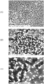
- FIG. 3 is an SEM image showing the surface state of the glassy carbon substrate processed by changing the processing time.
- the surface (processed surface) of the glassy carbon substrate is formed with a pattern consisting of minute protrusions having a shape that decreases in diameter toward the tip, and the height and pitch of the protrusions according to the processing time. Changed.
- X, Y and Z are all methoxy groups and (1) R is F (CF 2 ) 8 (8F2P3S3M), (2) F (CF 2 ) 10 by the following steps. (10F2P3S3M) and (3) F (CF 2 ) 12 (12F2P3S3M) were respectively synthesized.
- a 500 ml eggplant type flask equipped with a reflux condenser and a dropping funnel was replaced with a nitrogen atmosphere, 23.0 g (362 mmol) of copper bronze powder, 25.0 g (80.1 mmol) of 4,4′-dibromobiphenyl, and DMSO as a solvent. After adding 120 ml, the mixture was heated and stirred at 120 ° C. Two hours later, 23.6 ml (80.5 mmol) of perfluorooctyl iodide was slowly added dropwise, followed by heating and stirring at 120 ° C. for 24 hours. After the refluxing, the solution was cooled to room temperature, and excess copper powder and white solid were separated by filtration using a Kiriyama funnel.
- a 200 ml eggplant type flask equipped with a dropping funnel was replaced with a nitrogen atmosphere, cooled with dry ice / methanol refrigerant ( ⁇ 78 ° C.), and then 6.79 ml (18.1 mmol) of a 2.66M n-butyllithium / hexane solution. Then, 11.9 ml (9.04 mmol) of a 0.76 M isopropylmagnesium bromide / THF solution was added and stirred for 1 hour. Thereafter, 4.80 g (7.40 mmol) of 8F2PB dissolved in 50 ml of diethyl ether was slowly added dropwise, and the mixture was stirred at ⁇ 78 ° C. for 1 hour.
- the obtained distillate was identified as 8F2PA by 1 H-NMR, FT-IR, and Mass (m / z 612) spectra. Yield 1.86 g (3.04 mmol) Yield 41% Boiling point 164-167 ° C / 80Pa The property was a white solid.
- the obtained distillate was identified as 8F2P3S3M by 1 H-NMR, FT-IR, and Mass spectra. Yield 1.50 g (2.04 mmol) Yield 67% Boiling point 160-165 ° C / 30Pa The property was a white solid.
- a 500 ml eggplant type flask equipped with a reflux condenser and a dropping funnel was replaced with a nitrogen atmosphere, 20.0 g (315 mmol) of copper bronze powder, 20.0 g (64.1 mmol) of 4,4′-dibromobiphenyl, and DMSO as a solvent. After adding 120 ml, the mixture was heated and stirred at 120 ° C. After 2 hours, 42.6 g (66 mmol) of perfluorodecyl iodide was slowly added dropwise, followed by heating and stirring at 120 ° C. for 24 hours. After completion of the reflux, the solution was cooled to room temperature, and excess copper powder and white solid were separated by filtration using a Kiriyama funnel.
- a 200 ml eggplant type flask equipped with a dropping funnel was replaced with a nitrogen atmosphere and cooled with a dry ice / methanol refrigerant ( ⁇ 78 ° C.), and then 7.2 ml (19.2 mmol) of a 2.66M n-butyllithium / hexane solution. Subsequently, 0.73 M isopropylmagnesium bromide / THF solution (12.3 ml, 9.3 mmol) was added, and the mixture was stirred for 1 hour. Thereafter, 5.27 g (7.40 mmol) of 10F2PB dissolved in 50 ml of diethyl ether was slowly added dropwise and stirred at ⁇ 78 ° C. for 1 hour.
- a glass slide that had been washed by the above method was placed in a 200 ml wide-mouth receiver, and nitrogen substitution was performed.
- the modified solution prepared above was added to the wide-mouth receiver, and the slide glass was completely immersed in the modified solution, and heated and refluxed for 2 hours.
- the removed glass was washed with a modifying solvent and then with distilled water to change the methoxy group to an OH group.
- heat treatment is performed in an oven at 150 ° C. for 30 minutes for the purpose of constructing a siloxane network that forms a two-dimensional or three-dimensional network siloxane bond by condensation reaction with OH groups between adjacent silane coupling agents. It was. After the heat treatment, the glass was cooled to room temperature in a desiccator to obtain a modified glass.
- the contact angle of water with the modified glass was measured.
- the contact angle was measured using a droplet method in which a CA-X type contact angle measuring device manufactured by Kyowa Interface Science Co., Ltd. was used and 0.9 ⁇ l of water droplets were dropped on a horizontal glass plate to measure the contact angle.
- the glass surface modified with the silane coupling agent 8F2P3S3M shows a high contact angle after 2 hours at a temperature of 350 ° C.
- the modified glass using the silane coupling agent 8F2P3S3M solution maintains a high contact angle at 350 ° C. even after 8 hours.
- silane coupling agent 8F2P3S3M has higher heat resistance than 8F2P2S3M.
- the glass surface modified with the silane coupling agent 10F2P3S3M shows a high contact angle even after 2 hours at a temperature of 400 ° C.
- the modified glass using the silane coupling agent 10F2P3S3M solution maintains a high contact angle even after 10 hours at 400 ° C.
- the high contact angle with water shown in the above data indicates that the surface free energy is low, indicating that the releasability and antifouling properties are high.
- Example 1 A 0.5% solution of the synthesized 10F2P3S3M silane coupling agent (solvent: “HFE-7100” manufactured by Sumitomo 3M Limited) is applied to the processed surface (transfer pattern surface) of the glassy carbon substrate whose surface is processed by the ECR. After spin coating, it was baked at 130 ° C. for 10 minutes. Next, the transfer pattern surface was rinsed with HFE-7100. Thereby, a thin film of 10F2P3S3M silane coupling agent was formed on the transfer pattern surface of the glassy carbon substrate.
- solvent solvent: “HFE-7100” manufactured by Sumitomo 3M Limited
- PAK-02 a photocurable acrylic resin
- Toyo Gosei Co., Ltd. a photocurable acrylic resin
- PET polyethylene terephthalate
- PAK-02 was peeled from the glassy carbon substrate while holding the PET film.
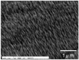
- FIGS. 7A to 7C are SEM images of 10,000 times, 30,000 times, and 60,000 times, respectively, observing the transfer surface of the resin.
- FIGS. 8A to 8C show the transfer surface of the resin. They are SEM images of 10,000 times, 30,000 times, and 60,000 times observed from an oblique direction (75 degrees), respectively. The transfer pattern of the glassy carbon matrix is accurately transferred.
- FIGS. 9A to 9C are SEM images of 10,000 times, 30,000 times and 60,000 times, respectively, observing the transfer pattern surface of the glassy carbon matrix after transfer, and the needle-like uneven pattern. The destruction of was not seen.
- FIGS. 10A to 10C are SEM images of 10,000 times, 30,000 times, and 60,000 times, respectively, when the transfer surface of the resin is observed. The transfer pattern of the glassy carbon matrix is accurately transferred.
- FIGS. 11A to 11C are SEM images of 10,000 times, 30,000 times, and 60,000 times, respectively, observing the transfer pattern surface of the glassy carbon matrix after transfer. The destruction of was not seen.
- Example 3 A Ni substrate (consisting only of Ni, hereinafter also referred to as a plated Ni plate) prepared by plating was first ultrasonically washed with acetone for about 15 minutes, then with ethanol for about 15 minutes, and then with ozone for about 1 hour. The surface of this plated Ni plate was coated with a 0.1% solution containing the synthesized 8F2P3S3M silane coupling agent (solvent: “HFE-7100” manufactured by Sumitomo 3M) by dipping for about 24 hours, and then HFE. After rinsing at ⁇ 7100 for about 1 minute, the mixture was heated at 150 ° C. for 30 minutes.
- solvent solvent: “HFE-7100” manufactured by Sumitomo 3M
- a photocurable acrylic resin (“PAK-01”, manufactured by Toyo Gosei Co., Ltd.) is applied to the surface of the plated Ni plate to which the silane coupling agent has been applied and cured, and then transferred by peeling it off.
- PAK-01 photocurable acrylic resin
- the contact angle was measured after resin peeling (transfer). The contact angle was measured at three points and the average value was calculated. After measuring the contact angle, it was rinsed with acetone and the next transfer was performed.
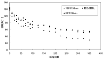
- the contact angle was measured by repeating the transfer in the same manner as described above.
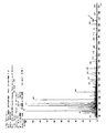
- the relationship between the number of transfers and the contact angle is shown in FIG. As can be seen in this figure, the contact angle decreases when the number of times of transfer is repeated, but the contact angle decreases when heat treatment is performed at 80 ° C and when heat treatment is not performed when compared with heat treatment performed at 150 ° C. Therefore, it can be said that it is advantageous when the transfer of a fine pattern is repeated.
- Example 4 The plated Ni plate was first ultrasonically washed with acetone for about 15 minutes, then with ethanol for about 15 minutes, and then ozone washed for about 1 hour. Next, a 0.1% solution containing the synthesized 10F2P3S3M silane coupling agent (solvent: “HFE-7100”, manufactured by Sumitomo 3M Ltd.) is used on the surface of the plated Ni plate, and heat treatment is not performed, and dipping is performed. After coating over a period of time, it was rinsed with HFE-7100 for about 1 minute, or after applying the silane coupling agent solution and heated at 80 ° C. for 30 minutes, the same rinsing was performed.
- solvent solvent: “HFE-7100”, manufactured by Sumitomo 3M Ltd.
- Example 3 the transfer was repeated in the same manner as in Example 3 to measure the contact angle. Further, when 8F2P3S3M is used as a mold release agent and when Durasurf 1101Z (manufactured by Harves) is used as a comparison, the contact angle is measured in the same manner as described above. The relationship is shown in FIG. As can be seen from this figure, when 8F2P3S3M is used and when 10F2P3S3M is used, the contact angle decreases less than when Durasurf is used, and it can be said that it is advantageous for transferring a fine pattern.
- the contact angle decrease is smaller than when 8F2P3S3M is used up to about 200 times of transfer, and it can be said that it is advantageous for transferring a fine pattern.
- the contact angle is generally smaller than when 8F2P3S3M or 10F2P3S3M is used, and the initial contact angle is 100 degrees or more. Was confirmed to occur.
- Example 5 Using the apparatus having the configuration shown in FIG. 2, the surface of the glassy carbon substrate (GC substrate) was finely processed under the following conditions. Beam irradiation angle: perpendicular to the processing surface (90 ° to the transfer pattern surface of the substrate) Reaction gas: Oxygen Gas flow rate: 3.0 SCCM Microwave: 100W Acceleration voltage: 500V Time: 20 minutes Vacuum: 1.3 ⁇ 10 ⁇ 2 Pa This finely processed surface is shown in FIG. A fine structure composed of a group of conical fine projections (pitch 53 nm, height 430 nm) is formed.
- FIG. 16 shows the transfer surface of the peeled PAK-01.
- An uneven pattern (pitch 110 nm, height 420 nm) on the finely processed surface of the GC substrate is transferred to PAK-01.
- a mold having a concavo-convex pattern having a height of 180 nm and a space width of 270 nm was produced on the Si substrate by SOG (Acuglass 512B manufactured by Honeywell) under the following conditions.
- EB exposure conditions Acceleration voltage: 10 KV Beam current: 10 pA
- Dose amount 800 ⁇ C / cm 2
- Development conditions-Developer BHF-Development time: 1 minute
- a mold having this concavo-convex pattern is treated with a 0.1% solution containing 8F2P3S3M silane coupling agent (solvent: "HFE-7100" manufactured by Sumitomo 3M) for 24 hours.
- Liquid phase treatment was performed, followed by rinsing with hydrofluoroether (Sumitomo 3M, HFE-7100) for 1 minute, followed by heating at 100 ° C. for 30 minutes.
- an Au film having a thickness of 330 mm was formed on the heat-treated silane coupling agent layer by vacuum vapor deposition using an apparatus of VPC-260F (manufactured by ULVAC KIKO).
- VPC-260F manufactured by ULVAC KIKO
- the PET substrate was pressed onto the Au film and heated at 90 ° C. for 10 minutes, and then the PET substrate was peeled off and observed with an SEM. As shown in FIG. The reflected Au film was transferred.
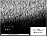
- Example 7 Using the apparatus having the configuration shown in FIG. 2, the surface of the glassy carbon substrate (GC substrate) was finely processed under the following conditions. Beam irradiation angle: perpendicular to the processing surface (90 ° to the transfer pattern surface of the substrate) Reaction gas: Oxygen Gas flow rate: 3.0 SCCM Microwave: 100W Acceleration voltage: 500V Time: 30 minutes Vacuum: 1.3 ⁇ 10 ⁇ 2 Pa This finely processed surface is shown in FIG. A fine structure pattern composed of a group of conical fine protrusions (pitch: 62 nm, height: 540 nm) is formed.
- a Cr film having a thickness of 30 nm was formed on the fine pattern, and an Au film having a thickness of 340 nm was further formed on the Cr film. Furthermore, after pressing the PET substrate onto the Au film and heating at 90 ° C. for 30 minutes, the PET substrate was peeled off and observed with an SEM. As shown in FIG. As a result, an Au film having a height of 550 nm and a pitch of 122 nm was transferred.
- a PET substrate having an Au film reflecting the irregularities of the mold was used as a mold, and this mold was used as a 0.1% solution containing 8F2P3S3M silane coupling agent (solvent: “HFE-7100, manufactured by Sumitomo 3M Limited). ))
- a photocurable resin PAK-01, manufactured by Toyo Gosei Kogyo Co., Ltd.
- the resin was cured by irradiating with ultraviolet rays at 5 J / cm 2 .
- the transferred and formed shape reflected the uneven shape of the mold formed on the first glassy carbon substrate, and had a height of 217 nm and a pitch of 91 nm.
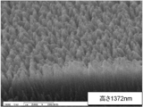
- Example 8> The surface of the glassy carbon substrate (10 mm square) was finely processed under the following conditions using the apparatus having the configuration shown in FIG. Acceleration voltage: 500 [V] Processing time: 60 [min] Gas type: O 2 Gas flow rate: 3.00 [SCCM]
- FIG. 23 shows the SEM image of the processed surface of the GC substrate after the processing, and
- FIG. 24 shows the reflectance.
- the height of the fine protrusions of the fine pattern formed on the processed surface was 1398 nm, and the pitch was 84 nm.
- the processed GC substrate was immersed in a 0.1% solution containing 8F2P3S3M silane coupling agent (solvent: “HFE-7100” manufactured by Sumitomo 3M Limited) for 1 hour, and then a photocurable resin (PAK-) was applied to the fine pattern.
- PAK- photocurable resin
- 02 manufactured by Toyo Gosei Kogyo Co., Ltd.
- a PET film was further pressed to perform UV irradiation (5 J / cm 2 ) from the PET film side to cure the resin.
- UV irradiation 5 J / cm 2
- FIG. 25 shows the resin layer transferred to the PET film.
- the antireflection structure according to the present invention has been described above, but the present invention is not limited to the above-described embodiments and examples.
- the matrix according to the present invention is manufactured using a glassy carbon substrate, it is not limited to the ECR type ion beam processing apparatus as shown in FIG. 2, and other processing apparatuses such as ICP may be used. Good.
Landscapes
- Engineering & Computer Science (AREA)
- Manufacturing & Machinery (AREA)
- Microelectronics & Electronic Packaging (AREA)
- Mechanical Engineering (AREA)
- Shaping Of Tube Ends By Bending Or Straightening (AREA)
- Manufacturing Of Printed Wiring (AREA)
Abstract
Priority Applications (2)
| Application Number | Priority Date | Filing Date | Title |
|---|---|---|---|
| US13/060,692 US8865049B2 (en) | 2008-09-05 | 2009-09-07 | Method for producing transfer structure and matrix for use therein |
| EP09811600.7A EP2330876B1 (fr) | 2008-09-05 | 2009-09-07 | Procédé de fabrication d'une structure de transfert et matrice pour une utilisation dedans |
Applications Claiming Priority (4)
| Application Number | Priority Date | Filing Date | Title |
|---|---|---|---|
| JP2008-228937 | 2008-09-05 | ||
| JP2008228937 | 2008-09-05 | ||
| JP2009-206479 | 2009-09-07 | ||
| JP2009206479A JP5419040B2 (ja) | 2008-09-05 | 2009-09-07 | 転写構造体の製造方法及びそれに用いる母型 |
Publications (1)
| Publication Number | Publication Date |
|---|---|
| WO2010027076A1 true WO2010027076A1 (fr) | 2010-03-11 |
Family
ID=41797239
Family Applications (1)
| Application Number | Title | Priority Date | Filing Date |
|---|---|---|---|
| PCT/JP2009/065612 WO2010027076A1 (fr) | 2008-09-05 | 2009-09-07 | Procédé de fabrication d'une structure transférée et matrice mère pour une utilisation dans le procédé |
Country Status (5)
| Country | Link |
|---|---|
| US (1) | US8865049B2 (fr) |
| EP (1) | EP2330876B1 (fr) |
| JP (1) | JP5419040B2 (fr) |
| KR (1) | KR101549063B1 (fr) |
| WO (1) | WO2010027076A1 (fr) |
Cited By (2)
| Publication number | Priority date | Publication date | Assignee | Title |
|---|---|---|---|---|
| JP2011184304A (ja) * | 2010-03-04 | 2011-09-22 | Tokyo Univ Of Science | シランカップリング剤及びその製造方法 |
| JP2012164787A (ja) * | 2011-02-07 | 2012-08-30 | Dainippon Printing Co Ltd | インプリント用モールド、およびインプリント方法 |
Families Citing this family (10)
| Publication number | Priority date | Publication date | Assignee | Title |
|---|---|---|---|---|
| JP5818306B2 (ja) * | 2011-03-07 | 2015-11-18 | 学校法人東京理科大学 | 転写構造体の製造方法及びそれに用いる母型 |
| JP5870627B2 (ja) * | 2011-11-01 | 2016-03-01 | 富士通株式会社 | 半導体装置の製造方法 |
| EP3012097A3 (fr) * | 2012-06-13 | 2016-06-22 | Asahi Kasei E-materials Corporation | Produit de transfert de fonction, procédé de transfert de couche fonctionnelle, produit conditionné et rouleau de film de transfert de fonction |
| US9587425B2 (en) * | 2013-09-13 | 2017-03-07 | 3M Innovative Properties Company | Vacuum glazing pillars delivery films and methods for insulated glass units |
| JP6277802B2 (ja) * | 2014-03-18 | 2018-02-14 | 富士通株式会社 | 電子部品の製造方法、電子部品および支持具 |
| JP6609402B2 (ja) * | 2014-06-19 | 2019-11-20 | デクセリアルズ株式会社 | 光学フィルム及びその製造方法 |
| CN106153178A (zh) * | 2015-03-17 | 2016-11-23 | 中国科学院苏州纳米技术与纳米仿生研究所 | 柔性导电振膜、柔性振动传感器及其制备方法和应用 |
| CN111094463A (zh) * | 2017-09-21 | 2020-05-01 | 捷德货币技术有限责任公司 | 产生具有预定内部和/或外部轮廓的颜料碎片的方法及颜料碎片 |
| JP7457645B2 (ja) * | 2018-03-09 | 2024-03-28 | 株式会社有沢製作所 | 積層体及びその製造方法 |
| KR102084911B1 (ko) * | 2018-12-05 | 2020-04-20 | 주식회사 델키 | 주방용 조리기구의 손잡이 구조 |
Citations (8)
| Publication number | Priority date | Publication date | Assignee | Title |
|---|---|---|---|---|
| JP2004063694A (ja) | 2002-07-26 | 2004-02-26 | Seiko Epson Corp | パターン転写フィルム、パターン転写フィルムの製造方法、機能性マスク、機能性マスクの製造方法 |
| JP2004107274A (ja) * | 2002-09-19 | 2004-04-08 | Norio Yoshino | 耐熱性シランカップリング剤、およびそれらの化合物の製造方法 |
| JP2005051095A (ja) * | 2003-07-30 | 2005-02-24 | Tdk Corp | 転写用基体およびその製造方法 |
| JP2007055975A (ja) | 2005-08-26 | 2007-03-08 | Mitsui Eng & Shipbuild Co Ltd | メタノール製造装置及びメタノール製造方法 |
| JP2007238567A (ja) * | 2006-03-10 | 2007-09-20 | Tokyo Univ Of Science | シランカップリング剤、歯科用コンポジットレジン、及びこのシランカップリング剤を含む歯科用プライマー |
| WO2008018570A1 (fr) | 2006-08-09 | 2008-02-14 | Tokyo University Of Science Educational Foundation Administrative Organization | Structure antireflet, procédé pour la produire et procédé pour produire un élément optique |
| JP2008054074A (ja) | 2006-08-25 | 2008-03-06 | Orion Denki Kk | ズーム機能を備えた光ディスク再生装置 |
| JP2008141167A (ja) * | 2006-09-29 | 2008-06-19 | Semiconductor Energy Lab Co Ltd | 導電層及び導電層を有する基板の形成方法、並びに半導体装置の作製方法 |
Family Cites Families (8)
| Publication number | Priority date | Publication date | Assignee | Title |
|---|---|---|---|---|
| US3565978A (en) * | 1967-09-11 | 1971-02-23 | Xerox Corp | Replication of surface deformation images |
| US3620895A (en) * | 1969-01-03 | 1971-11-16 | Polaroid Corp | Corrugated micropermeable membrane |
| US5204126A (en) * | 1990-02-06 | 1993-04-20 | Nanofilm Corporation | Mold surfaces with ultra thin release films |
| JPH10319222A (ja) * | 1997-05-16 | 1998-12-04 | Matsushita Electric Ind Co Ltd | 微細パターンの製造方法 |
| US7150844B2 (en) * | 2003-10-16 | 2006-12-19 | Seagate Technology Llc | Dry passivation process for stamper/imprinter family making for patterned recording media |
| JP2008063594A (ja) * | 2006-09-05 | 2008-03-21 | T & K:Kk | 含フッ素薄膜および該含フッ素薄膜を有する基材の製造方法 |
| JP5062521B2 (ja) * | 2007-02-27 | 2012-10-31 | 独立行政法人理化学研究所 | レプリカモールドの製造方法およびレプリカモールド |
| JP4487037B2 (ja) * | 2007-03-06 | 2010-06-23 | 学校法人東京理科大学 | 耐熱性、耐久性、離型性、及び防汚性シランカップリング剤、並びにそれらの化合物の製造方法 |
-
2009
- 2009-09-07 WO PCT/JP2009/065612 patent/WO2010027076A1/fr active Application Filing
- 2009-09-07 US US13/060,692 patent/US8865049B2/en not_active Expired - Fee Related
- 2009-09-07 JP JP2009206479A patent/JP5419040B2/ja not_active Expired - Fee Related
- 2009-09-07 KR KR1020117004063A patent/KR101549063B1/ko not_active IP Right Cessation
- 2009-09-07 EP EP09811600.7A patent/EP2330876B1/fr not_active Not-in-force
Patent Citations (9)
| Publication number | Priority date | Publication date | Assignee | Title |
|---|---|---|---|---|
| JP2004063694A (ja) | 2002-07-26 | 2004-02-26 | Seiko Epson Corp | パターン転写フィルム、パターン転写フィルムの製造方法、機能性マスク、機能性マスクの製造方法 |
| JP2004107274A (ja) * | 2002-09-19 | 2004-04-08 | Norio Yoshino | 耐熱性シランカップリング剤、およびそれらの化合物の製造方法 |
| JP2005051095A (ja) * | 2003-07-30 | 2005-02-24 | Tdk Corp | 転写用基体およびその製造方法 |
| JP2007055975A (ja) | 2005-08-26 | 2007-03-08 | Mitsui Eng & Shipbuild Co Ltd | メタノール製造装置及びメタノール製造方法 |
| JP2007238567A (ja) * | 2006-03-10 | 2007-09-20 | Tokyo Univ Of Science | シランカップリング剤、歯科用コンポジットレジン、及びこのシランカップリング剤を含む歯科用プライマー |
| WO2008018570A1 (fr) | 2006-08-09 | 2008-02-14 | Tokyo University Of Science Educational Foundation Administrative Organization | Structure antireflet, procédé pour la produire et procédé pour produire un élément optique |
| JP2008233850A (ja) | 2006-08-09 | 2008-10-02 | Tokyo Univ Of Science | 反射防止構造体及びその製造方法並びに光学部材の製造方法 |
| JP2008054074A (ja) | 2006-08-25 | 2008-03-06 | Orion Denki Kk | ズーム機能を備えた光ディスク再生装置 |
| JP2008141167A (ja) * | 2006-09-29 | 2008-06-19 | Semiconductor Energy Lab Co Ltd | 導電層及び導電層を有する基板の形成方法、並びに半導体装置の作製方法 |
Non-Patent Citations (1)
| Title |
|---|
| See also references of EP2330876A4 * |
Cited By (2)
| Publication number | Priority date | Publication date | Assignee | Title |
|---|---|---|---|---|
| JP2011184304A (ja) * | 2010-03-04 | 2011-09-22 | Tokyo Univ Of Science | シランカップリング剤及びその製造方法 |
| JP2012164787A (ja) * | 2011-02-07 | 2012-08-30 | Dainippon Printing Co Ltd | インプリント用モールド、およびインプリント方法 |
Also Published As
| Publication number | Publication date |
|---|---|
| US20110159245A1 (en) | 2011-06-30 |
| JP2010087500A (ja) | 2010-04-15 |
| EP2330876B1 (fr) | 2017-11-01 |
| KR20110063433A (ko) | 2011-06-10 |
| EP2330876A4 (fr) | 2015-11-04 |
| KR101549063B1 (ko) | 2015-09-01 |
| JP5419040B2 (ja) | 2014-02-19 |
| EP2330876A1 (fr) | 2011-06-08 |
| US8865049B2 (en) | 2014-10-21 |
Similar Documents
| Publication | Publication Date | Title |
|---|---|---|
| JP5419040B2 (ja) | 転写構造体の製造方法及びそれに用いる母型 | |
| US8344065B2 (en) | Nanoimprint resist, nanoimprint mold and nanoimprint lithography | |
| TWI628516B (zh) | 採用具有金屬或氧化物塗層之可重複使用聚合物模板的奈米壓印技術 | |
| TWI432892B (zh) | 供壓印微影術用之使用一黏著底層的方法 | |
| JP5818306B2 (ja) | 転写構造体の製造方法及びそれに用いる母型 | |
| US20220088834A1 (en) | Imprinting apparatus | |
| JP5578513B2 (ja) | 金属微細構造体の製造方法並びに樹脂成形物の製造方法 | |
| JP2005515617A (ja) | 非粘着性のモールドを使用する、パターン化された構造の複製 | |
| JP2016502227A (ja) | 熱融着転写を用いた柔軟埋込型電極フィルムの製造方法 | |
| JP5818252B2 (ja) | 金属膜パターン付き基体の製造方法 | |
| WO2013148126A1 (fr) | Photoréserves tridimensionnelles obtenues par fonctionnalisation de couches minces polymères fabriquées par icvd | |
| US20080003424A1 (en) | Particle Laminated Substate and Method for Manufacturing the Same | |
| JP5569927B2 (ja) | 金属膜を有する構造体の製造方法及びそれにより製造される構造体 | |
| KR102112029B1 (ko) | 나노 구조의 내부 집적형 개질층을 갖는 연료 전지 및 그 제조 방법 | |
| KR101291727B1 (ko) | 임프린트 레진의 제조방법 및 임프린팅 방법 | |
| US20150337494A1 (en) | Roller device using suction roller, and production method for member having uneven structure | |
| JP2010084162A (ja) | レプリカモールドの製造方法 | |
| KR20140099409A (ko) | 자기조립 단분자막의 표면 개질을 이용한 패턴의 전사 방법 | |
| KR100508108B1 (ko) | 중합체 패턴의 형성 방법 |
Legal Events
| Date | Code | Title | Description |
|---|---|---|---|
| 121 | Ep: the epo has been informed by wipo that ep was designated in this application |
Ref document number: 09811600 Country of ref document: EP Kind code of ref document: A1 |
|
| ENP | Entry into the national phase |
Ref document number: 20117004063 Country of ref document: KR Kind code of ref document: A |
|
| REEP | Request for entry into the european phase |
Ref document number: 2009811600 Country of ref document: EP |
|
| WWE | Wipo information: entry into national phase |
Ref document number: 2009811600 Country of ref document: EP |
|
| WWE | Wipo information: entry into national phase |
Ref document number: 13060692 Country of ref document: US |
|
| NENP | Non-entry into the national phase |
Ref country code: DE |