WO2010026843A1 - 慣性センサ - Google Patents
慣性センサ Download PDFInfo
- Publication number
- WO2010026843A1 WO2010026843A1 PCT/JP2009/063421 JP2009063421W WO2010026843A1 WO 2010026843 A1 WO2010026843 A1 WO 2010026843A1 JP 2009063421 W JP2009063421 W JP 2009063421W WO 2010026843 A1 WO2010026843 A1 WO 2010026843A1
- Authority
- WO
- WIPO (PCT)
- Prior art keywords
- inertial sensor
- detection
- movable
- unit
- detection unit
- Prior art date
Links
Images


Classifications
-
- G—PHYSICS
- G01—MEASURING; TESTING
- G01P—MEASURING LINEAR OR ANGULAR SPEED, ACCELERATION, DECELERATION, OR SHOCK; INDICATING PRESENCE, ABSENCE, OR DIRECTION, OF MOVEMENT
- G01P15/00—Measuring acceleration; Measuring deceleration; Measuring shock, i.e. sudden change of acceleration
- G01P15/02—Measuring acceleration; Measuring deceleration; Measuring shock, i.e. sudden change of acceleration by making use of inertia forces using solid seismic masses
- G01P15/08—Measuring acceleration; Measuring deceleration; Measuring shock, i.e. sudden change of acceleration by making use of inertia forces using solid seismic masses with conversion into electric or magnetic values
- G01P15/125—Measuring acceleration; Measuring deceleration; Measuring shock, i.e. sudden change of acceleration by making use of inertia forces using solid seismic masses with conversion into electric or magnetic values by capacitive pick-up
-
- G—PHYSICS
- G01—MEASURING; TESTING
- G01P—MEASURING LINEAR OR ANGULAR SPEED, ACCELERATION, DECELERATION, OR SHOCK; INDICATING PRESENCE, ABSENCE, OR DIRECTION, OF MOVEMENT
- G01P1/00—Details of instruments
- G01P1/02—Housings
- G01P1/023—Housings for acceleration measuring devices
-
- G—PHYSICS
- G01—MEASURING; TESTING
- G01P—MEASURING LINEAR OR ANGULAR SPEED, ACCELERATION, DECELERATION, OR SHOCK; INDICATING PRESENCE, ABSENCE, OR DIRECTION, OF MOVEMENT
- G01P15/00—Measuring acceleration; Measuring deceleration; Measuring shock, i.e. sudden change of acceleration
- G01P15/02—Measuring acceleration; Measuring deceleration; Measuring shock, i.e. sudden change of acceleration by making use of inertia forces using solid seismic masses
- G01P15/08—Measuring acceleration; Measuring deceleration; Measuring shock, i.e. sudden change of acceleration by making use of inertia forces using solid seismic masses with conversion into electric or magnetic values
- G01P2015/0805—Measuring acceleration; Measuring deceleration; Measuring shock, i.e. sudden change of acceleration by making use of inertia forces using solid seismic masses with conversion into electric or magnetic values being provided with a particular type of spring-mass-system for defining the displacement of a seismic mass due to an external acceleration
- G01P2015/0808—Measuring acceleration; Measuring deceleration; Measuring shock, i.e. sudden change of acceleration by making use of inertia forces using solid seismic masses with conversion into electric or magnetic values being provided with a particular type of spring-mass-system for defining the displacement of a seismic mass due to an external acceleration for defining in-plane movement of the mass, i.e. movement of the mass in the plane of the substrate
- G01P2015/0811—Measuring acceleration; Measuring deceleration; Measuring shock, i.e. sudden change of acceleration by making use of inertia forces using solid seismic masses with conversion into electric or magnetic values being provided with a particular type of spring-mass-system for defining the displacement of a seismic mass due to an external acceleration for defining in-plane movement of the mass, i.e. movement of the mass in the plane of the substrate for one single degree of freedom of movement of the mass
- G01P2015/0814—Measuring acceleration; Measuring deceleration; Measuring shock, i.e. sudden change of acceleration by making use of inertia forces using solid seismic masses with conversion into electric or magnetic values being provided with a particular type of spring-mass-system for defining the displacement of a seismic mass due to an external acceleration for defining in-plane movement of the mass, i.e. movement of the mass in the plane of the substrate for one single degree of freedom of movement of the mass for translational movement of the mass, e.g. shuttle type
Definitions
- the present invention relates to an inertial sensor that is formed by a microelectromechanical systems (MEMS) process and measures an inertial force such as applied acceleration by detecting a change in capacitance, and more particularly, a plurality of measurements.
- MEMS microelectromechanical systems
- the present invention relates to a technology that enables selection of a range.
- the general use of the acceleration sensor is organized according to its measurement range as follows.
- ⁇ 2G Measurements that require accuracy such as ride comfort, body shake, automatic transport vehicle, and posture in a stationary state.
- accuracy such as ride comfort, body shake, automatic transport vehicle, and posture in a stationary state.
- mobile phone posture measurement digital camera shake correction, inclinometer, automobile Adopted for suspension control and brake control of automobiles such as ABS (Antilock Brake System).
- ABS Antilock Brake System
- acceleration sensors often require different measurement ranges for various applications, and conventionally, a plurality of acceleration sensors with different output ranges have been supported.
- acceleration sensors having a plurality of measurement ranges with a single sensor have been developed in order to save space and reduce costs.
- an acceleration sensor with one sensor and multiple measurement ranges mainly the method of adjusting or selecting the measurement range by electrical signal processing and the integration of multiple sensors with different measurement ranges on one chip
- a method of sharing a circuit and a substrate, and a method of measuring a wide range with a single sensor have been developed.
- Patent Document 1 when measuring applied acceleration by differentially detecting a change in capacitance using a parallel plate type detection electrode, a plurality of detection signals having different frequencies and a filter matched therewith are detected.
- the control method of the accelerometer that can select the measurement range of acceleration by using.
- Patent Document 2 a plurality of acceleration sensors having greatly different measurement ranges are formed in one frame, so that the size can be reduced, and the plurality of acceleration sensors in the formation process include photolithography and etching.
- the manufacturing cost is low because a single chip can be formed in one step in the process, and the acceleration detection axes of a plurality of sensor elements can be matched with high accuracy by the mask accuracy of photolithography.
- the movable part of the acceleration sensor is composed of a plurality of divided movable parts, and the divided movable parts are connected to each other by a beam that can be elastically deformed.
- the acceleration detection sensitivity is improved and the acceleration response range is expanded. There is a description of that.
- Patent Document 1 the first problem of the conventional technology such as Patent Document 1 is that it is impossible to achieve both improvement in SNR (signal to noise ratio) and improvement in linearity of acceleration output.
- SNR signal to noise ratio
- linearity of acceleration output the general acceleration sensor examined as a premise of the present invention by the inventor will be described with reference to FIGS.
- the detection unit D1 includes a movable electrode D1a and fixed electrodes D1b and D1c, and a distance variation between the respective electrodes (displacement x of the movable electrode D1a).
- the detected change in capacitance ⁇ C is differentially detected by the electric circuit (sensor control / signal processing IC 100) shown in FIG. 2 to output the applied acceleration as a voltage signal.
- the applied acceleration a and the displacement x of the movable electrode D1a are expressed by the following equation (1) and are linear.
- x Displacement of the movable electrode D1a (movable part) a: Applied acceleration f0: Natural frequency of the acceleration sensor S1 m: Mass of the movable part k: Spring constant of the support beam on which the movable part is suspended.
- Expression (2) is a relational expression between the displacement x and the change in capacitance ⁇ C.
- the displacement x is 3 ⁇ m and 6 ⁇ m when the distance g between the movable electrode D1a and the fixed electrodes D1b and D1c is 3 ⁇ m and 6 ⁇ m. All the capacitance changes ⁇ C are shown. From FIG. 3 and the following equation (2), it can be seen that the capacitance change ⁇ C and the displacement x have a non-linear relationship.
- ⁇ dielectric constant of air
- A area between fixed electrodes D1b and D1c and movable electrode D1a
- g distance between fixed electrodes D1b and D1c and movable electrode D1a
- the output Vo of the acceleration sensor S1 includes the change in capacitance ⁇ C caused by the displacement x of the movable part 6 and the movable electrode D1a generated by the application of the acceleration a, and the carrier wave 101 applied to the fixed electrodes D1b and D1c of the detection part D1. Is obtained from the relational expression of the amplitude (voltage) Vi of the reference capacitor Cf and the reference capacitor Cf.
- Expression (3) describes an output relational expression of the acceleration sensor S1.
- the range of acceleration to be measured is ⁇ a
- the distance between the movable electrode D1a of the detection unit D1 and the fixed electrodes D1b and D1c is g
- the acceleration of ⁇ a is applied.
- the displacement x may be set to a value close to g as long as it does not collide.
- the capacitance change ⁇ C becomes extremely nonlinear as the displacement x approaches the interval g.
- the maximum value of the displacement x is determined by the non-linearity range allowed in the specification and the interval g.
- the maximum value of the displacement x is the widest range among the plurality of measurement ranges due to non-linearity limitations. It is necessary to decide together. Therefore, in the case of a narrow measurement range, there is a problem that the displacement x becomes small and the SNR is lowered (sacrificed).
- each vibration system can be configured depending on the size of the measurement range.
- the length and width of the movable part and the spring differ greatly.
- the processing error in processing may depend on the detailed shape of the mechanical structure constituting the sensor, but if a layout rule is determined, it often appears as a uniform dimensional shift in the wafer surface.
- This dimension shift uniformly shifts the width of the springs that make up each vibration system from the design value, so it has a large effect on sensor structures with a narrow measurement range, and it has an effect on sensor structures with a wide measurement range. small. For example, if a uniform size shift of ⁇ 0.5 ⁇ m occurs in the wafer, the support beam having a width of 3 ⁇ m is 2.5 ⁇ m, and the support beam having a width of 6 ⁇ m is 5.5 ⁇ m. Therefore, if the length of the support beam constituting each spring is constant, the respective spring constants are reduced by 42% and 23%, respectively, and the reduction amounts are different. The difference in the degree of influence for each structure results in a decrease in yield, making process management difficult. Naturally, since each vibration system is positionally independent from each other, the occupied area becomes large, which is disadvantageous for miniaturization.
- Patent Document 3 The third problem of the prior art such as Patent Document 3 is that a plurality of divided movable parts are connected to each other, and the measurement range is expanded by stopping the displacement of a part of the divided movable parts for each measurement range.
- the present invention solves the above-described problems, and its main object is to provide an inertial sensor such as an acceleration sensor that can be downsized and have a high SNR while having a plurality of measurement ranges. There is.
- the first is to provide an inertial sensor capable of achieving both improvement in linearity of SNR and acceleration output in all measurement ranges.
- a second object is to provide an inertial sensor that has a greatly different measurement range but is robust to processing errors and can be downsized.
- a third object is to provide an inertial sensor capable of obtaining an output range larger than the number of vibration systems composed of movable parts and springs.
- the outline of a typical one is characterized by having a plurality of detection ranges having different sensitivities defined by the ratio between the applied inertial force and the physical quantity generated from each detection unit, and having a plurality of measurement ranges. It is.
- N natural numbers of 2 or more
- (N + 1) or more measurement ranges are provided.
- a movable unit suspended on an elastic body via an elastic body, a movable unit formed on the movable unit, and a detection unit configured by a fixed electrode provided on the substrate.
- An inertial sensor that detects the inertial force of acceleration based on the change in capacitance of the detection unit, and the sensitivity differs when the ratio between the applied inertial force and the physical quantity generated from the detection unit is defined as the sensitivity
- a plurality of detection units are installed to obtain a plurality of range outputs.
- N movable parts includes N movable parts, a detection part that detects relative displacement of each movable part with respect to the fixed part, and a detection part (at least one) that detects relative displacement between the movable parts, Since N + 1 or more range outputs are obtained and the movable part and the spring are shared with each other, it is advantageous for miniaturization.
- the effect obtained by a typical one can provide an inertial sensor such as an acceleration sensor that can be downsized and have a high SNR while having a plurality of measurement ranges.
- FIG. 5 is a cross-sectional view showing a cross section taken along line A-A ′ of FIG. 4. It is sectional drawing which shows an example of the package structure which mounted the inertial sensor in Example 1 of this invention. It is explanatory drawing which shows the vibration system model of the inertial sensor in Example 1 of this invention.
- inertial sensor in Example 1 of this invention it is a graph which shows the nonlinearity with respect to a displacement, and an electrostatic capacitance change.
- FIG. 4 is a plan view illustrating an example of a main configuration of the inertial sensor according to the first embodiment.
- FIG. 5 is a cross-sectional view showing a cross section taken along line A-A ′ of FIG. 4.
- the inertial sensor S2 is formed by, for example, processing an SOI (Silicon On Insulator) substrate 1 by using photolithography and DRIE (Deep Reactive Ion Etching).
- SOI Silicon On Insulator
- DRIE Deep Reactive Ion Etching
- It may be manufactured using a so-called bulk MEMS process to be formed, or a thin film is deposited on the surface of a silicon substrate on which a signal processing circuit such as a transistor is formed in advance, and the deposited thin film is repeatedly patterned.
- the structure may be manufactured by using a so-called surface MEMS process.
- an intermediate insulating layer 1c is formed on a support substrate 1b, and an active layer (conductor layer) 1a is formed on the intermediate insulating layer 1c.
- the support substrate 1b is made of, for example, silicon (Si)
- the intermediate insulating layer 1c is made of, for example, silicon oxide (SiO 2 ).
- the active layer 1a formed on the intermediate insulating layer 1c is made of, for example, conductive silicon.
- the inertial sensor S2 of the first embodiment supports a fixed portion 2 supported and fixed to the support substrate 1b via the intermediate insulating layer 1c, and a movable portion 6 described later on the fixed portion 2 in a movable state.
- electrode pads 2e, D1be, D1ce, D2be, D2ce for exchanging signals with an external circuit by wire bonding or the like.
- the movable electrode D1a and the fixed electrodes D1b and D1c are arranged in a parallel plate shape, and form capacitances C1 and C2, respectively.
- the movable electrode D2a and the fixed electrodes D2b and D2c are arranged in parallel plates, and form capacitances C3 and C4, respectively.
- Each of the detection units D1 and D2 is configured to be capable of differential detection. For example, when the movable unit 6 is displaced in the + x direction, the detection unit D1 has a capacitance C1 and a capacitance that decrease in capacitance. The capacitance C2 increases.
- the detection unit D2 when the movable unit 6 is displaced in the + x direction, the detection unit D2 includes a capacitance C3 that reduces the capacitance and a capacitance C4 that increases the capacitance.
- These detection units D1 and D2 have different sensitivities (S) defined by the ratio between the inertial force of the applied acceleration and the physical quantity generated from each detection unit.
- inertial sensor S2 on the surface of one fixed portion 2 of the four fixed portions 2 that fix the movable portion 6 to the SOI substrate 1 so as to be movable by support beams 3 extending from the movable portion 6 in four directions. Is provided with an electrode pad 2e. It is also possible to provide the fixing portions 2 at four places. Further, electrode pads D1be and D1ce are provided on the surfaces of the outer end portions of the fixed electrodes D1b and D1c of the detection unit D1. Similarly, electrode pads D2be and D2ce are provided on the surface of the outer end of each electrode pad D2b and D2c of the detection unit D2.
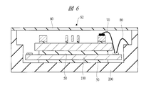
- FIG. 6 is a cross-sectional view showing an example of a package structure in which the inertial sensor S2 of the first embodiment is mounted.
- the package structure on which the inertial sensor S2 of the first embodiment is mounted uses a ceramic PKG (package) 200.
- the sensor control / signal processing IC 100 shown in FIG. 9 to be described later is mounted on the inner bottom surface of the concave portion of the ceramic PKG 200 via the adhesive 50.
- the inertial sensor S2 is mounted on the sensor control / signal processing IC 100 via the adhesive 50 again.
- the sensor control / signal processing IC 100 and the inertial sensor S2 are electrically connected by a wire 70 by wire bonding.
- the sensor control / signal processing IC 100 and the ceramic PKG 200 are electrically connected with a wire 80 and sealed with a lid 60, thereby completing an inertial sensor having a package structure.
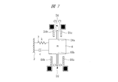
- the feature of the present invention is to have a plurality of detection units corresponding to each range in order to measure a plurality of ranges with one vibration system.
- one vibration system means a vibration structure that can be expressed by one movable part and one spring (corresponding to a support beam).
- the inertial sensor S2 shown in FIG. 4 is rewritten into a vibration system model constituted by the springs (spring constant k), the movable part, the damping (c), and the detection parts D1 and D2 for the convenience of explanation of functions, FIG. 7
- FIG. 7 is an explanatory view showing a vibration system model of the inertial sensor S2 of the first embodiment, and the same members are denoted by the same reference numerals so as to correspond to the actual shapes.
- the mass of the movable part 6 and the movable electrodes D1a and D2a is mainly m in the equation (1), and the total of the spring constants of the support beam 3 is k. Accordingly, the natural frequency f0 of the inertial sensor S2 and the displacement amount of the displacement x of the movable portion 6 when the acceleration a is applied in the detection direction (x direction) can be obtained from the equation (1).
- Capacitances C1 and C2 and capacitances C3 and C4 of the detection unit D2 change, respectively.
- This change in capacitance can be detected by a sensor control / signal processing IC 100 shown in FIG. That is, the change in capacitance is caused by the carrier wave 101 for detecting capacitance from the sensor control / signal processing IC 100 being applied to the electrode pads D1be and D1ce of the detection unit D1 and the electrode pads D2be and D2ce of the detection unit D2.
- a differential input is made to the CV conversion unit 102 of the sensor control / signal processing IC 100 via the electrode pad (common electrode) 2e connected to the movable unit 6.
- the change in capacitance is converted into a voltage signal.
- only the necessary signal component is extracted by the synchronous detection circuit 103, and finally converted into a digital value by the A / D conversion unit 104. Output to.
- an acceleration sensor that detects the acceleration ranges ⁇ 2G and ⁇ 4G with a detection nonlinearity of ⁇ 1%.
- the input of the capacitance change ( ⁇ C) at which the CV conversion unit 102 of the sensor control / signal processing IC 100 is saturated is 0.25 pF, and the movable electrode of the detection unit D1 among the plurality of detection units D1 and D2
- An interval g between D1a and the fixed electrodes D1b and D1c is 3 ⁇ m.
- the interval g is often determined by process restrictions.
- the initial capacitance is proportional to the opposing area A of both electrodes forming the capacitance and inversely proportional to the gap g between the electrodes. Therefore, the smaller the gap g is, the smaller the facing area A can be, resulting in a reduction in size.
- the natural frequency f0 of the inertial sensor S2 and another detection unit D2 may be designed based on the concept of the first embodiment (the present invention).
- the natural frequency f0 is determined by the narrower interval g (here, the interval of the detection unit D1 is 3 ⁇ m) and the nonlinearity specification ⁇ 1% among the detection units D1 and D2.
- FIG. 8 is an enlarged view of a part of FIG. 3 with detection nonlinearity at the displacement x of the movable portion 6 added. That is, FIG. 8 is a graph showing nonlinearity NL and capacitance change ⁇ C with respect to displacement x.
- the definition of the non-linearity NL is obtained by substituting 0 as the displacement x into the capacity change rate of the detection unit when the displacement x is 0, that is, the equation (2) differentiated from the displacement x. This is the ratio of the capacitance change ⁇ C actually obtained by the displacement x to the ideal capacitance change line obtained by multiplying the obtained value (sensitivity S) by the displacement x. Equation (4) below shows the definition of sensitivity S, and equation (5) shows the definition of nonlinearity NL.
- FIG. 8 shows that when the distance g of the detection part D1 is 3 ⁇ m, the displacement x that satisfies the nonlinearity NL of ⁇ 1% or less is ⁇ 0.3 ⁇ m.
- the displacement x that satisfies the nonlinearity NL of ⁇ 1% or less is ⁇ 0.3 ⁇ m.
- ⁇ C larger than the assumed capacitance change ⁇ C is generated due to the influence of vibration disturbance other than the signal component. Therefore, in actual design, it is necessary to design with a margin in nonlinearity.
- the description is omitted because it is not related to the essence of the invention. However, even in this case, the basic concept of the present invention can be applied.
- the natural frequency f0 is determined from the relational expression between the displacement x and the natural frequency f0 in the equation (1).
- the natural frequency f0 is 1300 Hz.
- the design of the detection unit D2 will be described.
- the displacement x when ⁇ 4 G is applied is ⁇ 0.6 ⁇ m from the equation (1). Accordingly, when the displacement x becomes ⁇ 0.6 ⁇ m, the distance g between the movable electrode D2a of the detection unit D2 and the fixed electrodes D2b and D2c at which the nonlinearity NL becomes ⁇ 1% may be determined. 6 ⁇ m (see FIG. 8).
- the initial capacitances C3 and C4 of the detection unit D2 are also reduced, so that the absolute value of ⁇ C when ⁇ 4G is applied is also reduced.
- the ratio of the capacitance change ⁇ C of the detection unit D1 when ⁇ 2G is applied to the capacitance change ⁇ C of the detection unit D2 when ⁇ 4G is applied is 7.43. Therefore, the CV conversion unit 102 can be shared by increasing the electrode size of the detection unit D2 to 7.43 times that of the detection unit D1.
- the scale of the detection unit D2 is increased by increasing the facing area A between the electrodes.
- both the detection units D1 and D2 have the same capacitance change ⁇ C with respect to the maximum measured acceleration ( ⁇ 2G and ⁇ 4G). That is, the change value of the capacitance when the maximum acceleration that can be measured for each measurement range of each of the detection units D1 and D2 is applied is the same value.
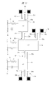
- FIG. 9 is a configuration diagram illustrating an example of an electrical configuration of the inertial sensor S2 according to the first embodiment. In FIG. 9, selection of each range and the processing method of the detection part which is not selected are demonstrated.
- the inertial sensor S2 includes, in an electrical configuration, a sensor control / signal processing IC 100 connected to a mechanical structure including the detection units D1 and D2 and the movable unit 6 as described above, and a changeover switch monitor. 107 and the like, and an external input 108 is possible.
- the sensor control / signal processing IC 100 includes a CV conversion unit 102 that converts a capacitance change value of the detection units D1 and D2 into a voltage value, a synchronous detection circuit 103 that synchronously detects an output from the CV conversion unit 102, An A / D converter 104 for analog / digital conversion of the output from the detection circuit 103, and an output value from the CV converter 102 (specifically, an output of the A / D converter 104 after synchronous detection and analog / digital conversion) Value) exceeds a certain range, the overrange determination unit 105, the carrier wave 101 applied to the detection units D1, D2 based on the output signal from the overrange determination unit 105, and the signals from the detection units D1, D2
- a range changeover switch 106 is provided for switching between the measurement range, and the range changeover switch 106 is a switch for selecting one of the measurement ranges. Even functioning.
- the inertial sensor S2 of the first embodiment can cope with a method of manually switching the measurement range and a method of automatically switching the measurement range.
- the range changeover switch 106 in FIG. 9 is set to state 1, and the carrier wave 101 is applied to the detection unit D1 ( ⁇ 2G range).
- the detection unit D2 is connected to a common potential and has the same potential as the DC level of the movable unit 6.
- the CV conversion unit 102 is saturated or the voltage at the output terminal of the A / D conversion unit 104 exceeds a certain value.
- the movable part 6 When the acceleration is applied, the movable part 6 is displaced in the direction opposite to the acceleration according to the law of inertia. At this time, a change in electrostatic capacitance between the movable electrode D1a of the detection unit D1 and the fixed electrodes D1b and D1c and between the movable electrode D2a of the detection unit D2 and the fixed electrodes D2b and D2c is changed to a change in voltage value by the CV conversion unit 102. After the conversion and further synchronous detection by the synchronous detection circuit 103, the analog value is converted into a digital value by the A / D converter 104.
- the overrange determination unit 105 determines whether or not it is overrange based on the output value from the A / D conversion unit 104, and in the case of overrange (yes), controls the state of the range changeover switch 106. Is switched to a wider measurement range (from state 1 to state 2) by switching the range changeover switch 106. On the other hand, when it is not the overrange (no), it is not necessary to switch to the wide measurement range, so that the state 1 remains.
- the range changeover switch 106 outputs the current state to an external changeover switch monitor 107 to notify the selected measurement range to the outside.
- the range selector switch 106 is switched from state 1 to state 2 by the external input 108.
- ⁇ 2G and ⁇ 4G measurement ranges can be selected.
- the measurement range is limited by the natural frequency f0 of the inertial sensor S2 and the interval between the movable electrode and the fixed electrode in the detection units D1 and D2, which is narrower.
- ⁇ 4G the distance between the movable electrode D1a of the detection unit D1 and the fixed electrodes D1b and D1c is 3 ⁇ m, and when the acceleration of 20 G is applied from the equation (1), The movable electrode D1a of the detection unit D1 and the fixed electrodes D1b and D1c are in physical contact. Therefore, the measurement limit of the inertial sensor S2 is 20G.
- the natural frequency f0 may be increased. From the relationship of the formula (1), if the natural frequency f0 is increased five times, the measurable range is 25 times. That is, when f0 is 1300 Hz, the output range which was ⁇ 2 G and ⁇ 4 G becomes ⁇ 50 G and ⁇ 100 G by changing f0 to 6500 Hz. In addition, the number of measurement ranges that can be selected is increased by adding detectors with different sensitivities S.
- the inertial sensor S2 By performing the design procedure of the inertial sensor S2 in the first embodiment described above, it is possible to provide an inertial sensor that can ensure the maximum SNR and acceleration output linearity below a specified value in all measurement ranges. . That is, a plurality of range outputs are obtained by a plurality of detection units D1 and D2 having different sensitivities (S: Formula (4)) defined by the ratio between the applied acceleration and the physical quantity generated from the detection unit. , SNR and acceleration output linearity can be improved at the same time.
- Example 2 The greatest feature of the inertial sensor in Example 2 is that it has two greatly different measurement ranges. Although the inertial sensor described in the first embodiment has a plurality of ranges, the ratio between the ranges is 5 due to the gap g between the electrodes that can be actually manufactured together and the size of the mechanical structure. The following will be realistic.
- the inertial sensor according to the second embodiment includes a plurality of movable parts, a detection part that detects relative displacement of each movable part with respect to the fixed part, and a detection part (at least one) that detects relative displacement between the movable parts.
- the ratio between the measurement ranges is 10 or more.
- FIG. 10 is a plan view illustrating an example of a main configuration of the inertial sensor according to the second embodiment.
- the inertial sensor S3 is capable of moving fixed portions 2a, 2b, and 2c supported and fixed to the support substrate 1b, and movable portions 6a, 6b, and 6c described later on the fixed portions 2a, 2b, and 2c, respectively.
- Support beams 3a, 3b, 3c supported in a state, and movable parts 6a, 6b, 6c that are suspended by the support beams 3a, 3b, 3c and are displaced following the acceleration when acceleration is applied.
- detection units D1, D2, D3, and D4 for detecting the displacement amounts of the movable units 6a, 6b, and 6c, and electrode pads (not shown) for exchanging signals with an external circuit by wire bonding or the like. It consists of
- the detection unit D1 is a detection unit that detects a relative displacement of the movable unit 6a with respect to the fixed unit 2a, and the movable electrode D1a and the fixed electrodes D1b and D1c are arranged in a parallel plate shape.
- the detection unit D2 is a detection unit that detects a relative displacement between the movable unit 6a and the movable units 6b and 6c.
- One movable electrode D2a and the fixed electrode D2b, and the other movable electrode D2a and the fixed electrode D2c are parallel to each other. It is arranged in a flat plate shape.
- the detection unit D3 is a detection unit that detects relative displacement of the movable unit 6b with respect to the fixed unit 2b, and the movable electrode D3a and the fixed electrodes D3b and D3c are arranged in a parallel plate shape.
- the detection unit D4 is also a detection unit that detects relative displacement of the movable unit 6c with respect to the fixed unit 2c, and the movable electrode D4a and the fixed electrodes D4b and D4c are arranged in a parallel plate shape.
- the manufacturing process and mounting form of the inertial sensor S3 of the second embodiment are the same as those of the first embodiment, the description thereof will be omitted, and why a greatly different measurement range, which is a feature of the second embodiment, is possible. And why it can be realized by a detection unit having a similar shape such as an interval will be described in detail.
- a specific measurement range of ⁇ 2G and ⁇ 100G will be described as an example.
- FIG. 11 is an explanatory diagram showing a vibration system model of the inertial sensor S3 of the second embodiment, and the same reference numerals are assigned to the same members so as to correspond to the actual shapes.
- the inertial sensor S3 of the second embodiment is configured as three vibration systems.
- the first vibration system is composed of a movable part 6a, a spring (support beam 3a), and detection parts D1, D2, and the second vibration system is composed of a movable part 6b, a spring (support beam 3b), and detection parts D2, D3.
- the third vibration system includes a movable part 6c, a spring (support beam 3c), and detection parts D2 and D4.
- a wide measurement range (for example, ⁇ 100 G) is measured using the displacement difference between the displacement x1 and x2 or x3. That is, the greatest feature of the second embodiment is that a wide measurement range is measured by using a relative displacement (displacement difference) between the plurality of movable parts 6a and 6b.
- the input of the capacitance change ( ⁇ C) at which the CV conversion section 102 (see FIG. 12 described later) of the sensor control / signal processing IC 100 is saturated is 0.25 pF, and the process
- the distance g between the movable electrode and the fixed electrode of the detection unit is set to 3 ⁇ m due to physical restrictions.
- the output nonlinearity is also set to ⁇ 1% or less.
- the inertial sensor S3 detects an acceleration of ⁇ 100G
- the natural frequency at which the displacement x is 3 ⁇ m is 2877 Hz.
- the natural frequency of the first vibration system is f1 is set to 3000 Hz. Since the natural frequency f1 is set to 3000 Hz, the displacement amount x1 of the movable portion 6a of the first vibration system when ⁇ 2G is applied is 55 nm, which is 300 nm or less as shown in FIG. % Or less is satisfied.
- the electrode scale that is 5.3 times that of the detection unit of the inertial sensor S2 of the first embodiment is required.
- the thickness of the active layer 1a is 40 ⁇ m, and the movable electrode D1a and the fixed electrodes D1b and D1c of the detection unit D1 overlap. Since the thickness is 200 ⁇ m, the number of electrodes is 140.
- the detection unit D1 is a parallel plate type capacitance detection method. When the width of the comb teeth constituting the movable electrode and the fixed electrode is 4 ⁇ m, the length required to form the detection unit D1 is 2940 ⁇ m. Thus, since the electrodes are formed on both sides of the movable portion 6a, the first vibration system has a size of approximately 1.5 mm ⁇ 1.5 mm. The size of the inertial sensor can be further reduced if the aspect ratio defined as the ratio of the distance g between the detection portions D1 and the thickness of the active layer 1a can be increased.
- the natural frequencies f2 and f3 of the second and third vibration systems will be described.
- the natural frequencies f2 and f3 are set to 300 nm so that the relative displacement between the movable parts 6a and 6b or 6c when applying ⁇ 100G is as small as possible while the nonlinearity satisfies ⁇ 1% or less.
- the natural frequencies f2 and f3 are set to 3178 Hz from the above equation (1), the relative displacement (x1-x2 or x1-x3) between the movable parts 6a and 6b or 6c when ⁇ 100 G is applied is 300 nm, and the nonlinearity is reduced. While satisfying the specification of ⁇ 1% or less, it is possible to form the detection unit D2 having a capacitance change ⁇ C of 0.25 pF with an electrode scale approximately one-third of the detection unit D1.
- the natural frequency f1 of the first vibration system is set to 3000 Hz
- the natural frequencies f2 and f3 of the second and third vibration systems are set to 3178 Hz.
- the natural frequency f2 and f3 may be 3000 Hz.
- the detection part D1 with a large electrode scale can be arranged around the inertial sensor S3, it is advantageous for downsizing.
- the detection units (which also have the function of the natural frequency adjusting unit, which will be described as the natural frequency adjusting unit in the following) D3 and D4 will be described with reference to FIG.
- the inertial sensor S3 of the second embodiment it is already known by applying a DC voltage between the movable electrodes D3a, D4a and the fixed electrodes D3b, D3c, D4b, D4c of the natural frequency adjusting units D3, D4.
- the natural frequencies f2 and f3 of the second and third vibration systems including the movable parts 6b and 6c are adjusted using the electrostatic spring effect.
- the relative displacement between the movable part 6a and the movable parts 6b and 6c is used for the measurement of ⁇ 100G. Therefore, the movable parts 6b and 6c need to have the same displacement per unit acceleration.
- the second and third vibration systems including the movable parts 6b and 6c are separated from each other and are configured as independent vibration systems, the natural frequencies of the respective vibration systems are made to exactly match from the influence of processing errors. It is almost impossible. Therefore, by providing the natural frequency adjusting units D3 and D4, the natural frequencies f2 and f3 of the second and third vibration systems are adjusted.
- the inertial sensor S3 is vibrated AC at the time of shipment, and the DC voltages 109 and 110 applied to the natural frequency adjusting units D3 and D4 are adjusted so that the DC level output of the inertial sensor S3 becomes zero. (See FIG. 12).
- the natural frequency adjusting units D3 and D4 have the same configuration as the detecting unit D1, the natural frequency adjusting units D3 and D4 can also be used to detect the displacements x2 and x3 of the movable units 6b and 6c.
- the difference between the natural frequencies f1 of the first vibration system and the natural frequencies f2 and f3 of the second and third vibration systems is large. Therefore, the deviation of the natural frequency due to the processing error can be almost ignored, and the number of measurement ranges can be increased by diverting the natural frequency adjustment units D3 and D4 as the detection unit.
- FIG. 12 shows an electrical configuration of the inertial sensor S3 of the second embodiment, and shows a case where the D3 and D4 are used as the natural frequency adjusting unit, respectively.
- the natural frequency adjusting units D3 and D4 are used as detecting units for detecting the displacements x2 and x3 of the movable units 6b and 6c, the carrier wave 101 is applied to the natural frequency adjusting units D3 and D4. That's fine.
- the measurement range can be switched manually through the external input 108 or automatically through the overrange determination unit 105. Since the specific contents for switching the measurement range are the same as those of the inertial sensor S2 of the first embodiment, description thereof is omitted.
- the detection portions D1, D2, D3, and D4 are similar in shape such as the distance between them, and the shapes of the movable portions 6a, 6b, and 6c and the springs (support beams 3a, 3b, and 3c) constituting each vibration system.
- the influence of the processing error on the performance variation is relatively small, the processing error is robust, and downsizing can be realized.
- the third embodiment is an inertial sensor having a plurality of measurement ranges, in which a plurality of vibration systems composed of a plurality of movable parts and springs are connected to each other. It is characterized by having a measurement range of +1 or more vibration systems by measuring the relative displacement between the parts, and because each vibration system shares a movable part and a spring with each other, which is advantageous for downsizing.
- the third embodiment will be described in detail with reference to the drawings.
- the same reference numerals are given to portions overlapping with the first and second embodiments, and the description thereof is omitted.
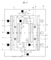
- FIG. 13 is a plan view illustrating an example of a main configuration of the inertial sensor according to the third embodiment.
- the inertial sensor S4 according to the third embodiment has fixed portions 2a, 2b, and 2c supported and fixed to the support substrate 1b, and a support that supports a movable portion 6b, which will be described later, on the fixed portions 2a, 2b, and 2c in a movable state.
- the detection unit D1 one movable electrode D1a and the fixed electrode D1b, and the other movable electrode D1a and the fixed electrode D1c are arranged in a parallel plate shape.
- the detection unit D2 includes one movable electrode D2a and fixed electrode D2b, the other movable electrode D2a and fixed electrode D2c
- the detection unit D3 includes one movable electrode D3a and fixed electrode D3b, and the other movable electrode D2b.
- Each of the electrode D3a and the fixed electrode D3c is arranged in a parallel plate shape.
- the inertial sensor S4 of the third embodiment is an inertial sensor configured as two vibration systems.
- the present invention is not limited to two vibration systems, and may be configured as N vibration systems.
- the measurement range when it is configured as N vibration systems is N + 1 or more.
- FIG. 14 is an explanatory diagram showing a vibration system model of the inertial sensor S4 of the third embodiment.
- the same reference numerals are assigned to the same members so as to correspond to the actual shapes.
- the inertial sensor S4 according to the third embodiment includes a first vibration system that includes a movable portion 6a (movable portion m1) and a spring (support beam 3a), a movable portion 6b (movable portion m2), and a spring (support beam 3b). This is configured as a second vibration system.
- the second vibration system is divided into three equal parts by the insulating film 7 in which the movable portion 6b is an insulating material, and the movable portions 6b1, 6b2, and 6b3 are mechanically connected and electrically separated. ing.
- the insulating film 7 is formed by deepening the active layer 1a by DRIE and embedding an insulating film such as an oxide film by thick film CVD (Chemical Vapor Deposition) or the like. Further, the insulating film 7 prevents the movable parts 6b1, 6b2 and 6b3 from breaking at the interface of the insulating film 7 at least once as shown in FIG. 13 (four examples in FIG. 13). Is formed as a bent shape.
- the measurement range of the inertial sensor S4 of the third embodiment is to measure the displacement x1 of the first movable part 6a, the displacement x2 of the second movable part 6b, and the relative displacement xr of the movable parts 6a and 6b. Three can be selected.
- the inertial sensor S4 of the present embodiment has a first mode natural frequency in which the two movable parts 6a and 6b vibrate in the same phase in the several kHz band.
- the acceleration sensor mainly measures frequency components of several tens to 100 Hz or less, and there is no phase difference between the displacements of the movable parts 6a and 6b. This is the sum of the displacement x2 and the relative displacement xr of the movable parts 6a and 6b. Therefore, the relationship of x1> x2 is established for all acceleration applications.
- the displacement amounts x1, x2, and xr can be obtained by using the equation (1).
- the relative displacement xr of the movable parts 6a and 6b is determined when the vibration system model shown in FIG. 14 is regarded as two independent one-degree-of-freedom systems, and the movable electrode 6a and the movable electrodes D1a of the detection parts D1 and D2.
- D2a is m
- the spring constant of the support beam 3a that supports the movable portion 6a is k, and is obtained by substituting the first natural frequency f1 obtained by substituting into the equation (1). .
- the displacement amount x2 is the displacement of the movable part 6b.
- the second natural frequency f2 obtained by setting the mass of the movable electrode D2a of the portion D2 to m and the spring constant of the support beam 3b supporting the movable portion 6b to k is substituted into the equation (1). Is required.
- the displacement x1 of the movable portion 6a with respect to the support substrate 1b can be obtained as the sum of the displacements x2 and xr. By detecting the displacements x1, xr, and x2 using the detection units D1, D2, and D3, respectively, three measurement ranges can be obtained.
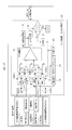
- FIG. 15 shows an electrical configuration of the inertial sensor S4 of the third embodiment.
- the three measurement ranges are switched automatically or manually by using an overrange determination unit 105, a range changeover switch 106, and an external input 108. be able to.
- an overrange determination unit 105 a range changeover switch 106
- an external input 108 an external input 108.
- the range changeover switch 106 has three states according to the measurement range. First, in state 1, the carrier wave 101 is applied to the movable part 6a via the movable part 6b2, and the outputs from the fixed electrodes D1b and D1c of the detection part D1 are input to the CV conversion part 102, whereby the displacement of the movable part 6a. x1 is detected. At this time, the other detection units D2 and D3 and the movable units 6b1 and 6b3 are connected to the DC bias of the CV conversion unit 102.
- the carrier wave 101 is applied to the movable part 6a via the movable part 6b2, and the outputs from the fixed electrodes D2b and D2c of the detection part D2 are respectively transmitted via the movable parts 6b1 and 6b2.
- the relative displacement xr of the movable parts 6a and 6b is detected by inputting it to the CV conversion part 102.
- the other detection units D 1 and D 3 are connected to the DC bias of the CV conversion unit 102.
- the carrier wave 101 is applied to the movable parts 6b1 and 6b3, and the outputs from the fixed electrodes D3b and D3c of the detection part (natural frequency adjustment part) D3 are input to the CV conversion part 102, thereby moving the state.
- the displacement x2 of the part 6b is detected.
- the movable part 6b2 and the other detection part D1 are connected to the DC bias of the CV conversion part 102.
- the relative displacement between the vibration systems is measured while having N vibration systems so that three measurement ranges can be obtained with the two vibration systems.
- N + 1 measurement ranges can be obtained. That is, it is possible to obtain an output range that is larger than the number of vibration systems configured by the movable parts 6a and 6b and the springs (support beams 3a and 3b).
- the inertial sensor according to the present invention can be used in a wide variety of applications such as automobiles, portable devices, amusement devices, and information appliances.
Abstract
複数の測定レンジを持ちながらも小型化かつ高いSNRを得ることが可能な加速度センサなどの慣性センサを提供するため、検出部の静電容量の変化に基づいて加速度の慣性力を検出する慣性センサにおいて、印加された慣性力と各検出部から発生する物理量との比で定義した感度が異なる複数の検出部D1~D4を備え、複数の測定レンジを有する。または、N(2以上の自然数)個の可動部6a~6cを備える場合に、(N+1)個以上の測定レンジを有する。
Description
本発明は、半導体微細加工技術(microelectromechanical systems(MEMS)プロセス)により形成され、印加された加速度などの慣性力を静電容量の変化を検出することで測定する慣性センサに関し、特に、複数の測定レンジを選択可能とする技術に関する。
例えば、慣性センサに関して、一般的な加速度センサの用途をその測定レンジ別に整理してみると、以下のようになる。
(1)±2G:乗り心地、身体の動揺、自動搬送車、静止状態での姿勢など、精度を要する測定であり、例えば、携帯電話機の姿勢測定、デジタルカメラの手ぶれ補正、傾斜計、自動車のサスペンション制御やABS(Antilock Brake System)など自動車のブレーキ制御などに採用。
(2)±4G:四肢の動きなどの測定であり、例えば、ゲーム機のリモコンなどアミューズメントとコンピュータのヒューマンインタフェースに採用。
(3)±30G~50G:主に自動車のエアーバック用としてECU(Electronic Control Unit)側に取り付けられるセンサとして採用。
(4)±50G~250G:主に自動車のエアーバック用として車両の前方もしくは後方に取り付けられるセンサとして採用。
上述のように加速度センサは様々な用途で夫々の測定レンジが必要とされる場合が多く、従来では出力レンジが異なる複数の加速度センサで対応してきた。しかし、最近は、省スペース、低コスト化の要求から、一つのセンサで複数の測定レンジを持つ加速度センサも開発されている。
一つのセンサで複数の測定レンジを持つ加速度センサとしては、主に、電気的な信号処理によって測定レンジを調整もしくは選択する方法と、測定レンジが違う複数のセンサを一つのチップに集積し、周辺回路や基板などを共有する方法、一つのセンサで広い範囲のレンジを測定する方法が開発されている。
例えば、特許文献1には、並行平板型の検出電極を用いて静電容量の変化を差動検出することで印加された加速度を測定する際、周波数が異なる複数の検波信号とそれに合わせたフィルタを使うことで、加速度の測定レンジが選択できる加速度計の制御方法についての記述がある。
また、特許文献2には、測定レンジの大きく異なる複数の加速度センサを一つの枠の中に形成しているため、小型化ができることと、形成プロセス上複数の加速度センサはフォトリソグラフィやエッチングなどの工程で一つのチップに一括形成できるので製造コストが低く、かつ複数のセンサ素子の加速度検出軸をフォトリソグラフィのマスク精度で高精度に一致させることができることの記述がある。
また、特許文献3には、加速度センサの可動部を複数の分割可動部から構成し、この分割可動部同士を弾性変形可能な梁で接続する。各分割可動部の可動範囲、質量、各梁の剛性等を調整する、または、加速度に対する感度領域の異なる複数の変形モードを併用することにより、加速度の検出感度を向上させるとともに加速度応答範囲を広げることの記述がある。
ところで、前述したような加速度センサに関して、本発明者が検討した結果、以下のようなことが明らかとなった。
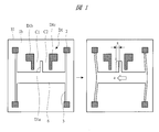
例えば、前記特許文献1などの従来技術の第1の問題点は、SNR(signal to noise ratio)の向上と、加速度出力の線形性向上の両立ができないことである。ここで、本発明者が本発明の前提として検討した一般的な加速度センサを示す図1~図3を用いて説明する。
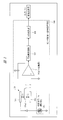
一つの加速度検出部を用いて電気的な信号処理によって複数のレンジを持たせた場合、測定レンジが狭い方のSNRが犠牲される。図1に示している並行平板型の加速度センサS1の場合、検出部D1は、可動電極D1aと固定電極D1b,D1cとで構成され、夫々の電極間の距離変動(可動電極D1aの変位x)に伴う静電容量の変化ΔCを図2に示す電気回路(センサ制御・信号処理用IC100)で差動検出することで、印加された加速度を電圧信号として出力する。印加される加速度aと可動電極D1aの変位xは下記式(1)の関係となり、線形である。

式(1)において、
x:可動電極D1a(可動部)の変位
a:印加される加速度
f0:加速度センサS1の固有振動数
m:可動部の質量
k:可動部を懸架している支持梁のばね定数
を示す。
x:可動電極D1a(可動部)の変位
a:印加される加速度
f0:加速度センサS1の固有振動数
m:可動部の質量
k:可動部を懸架している支持梁のばね定数
を示す。
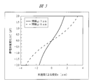
しかし、並行平板型の検出部D1の場合、変位xに対しての静電容量の変化ΔC(ΔC=C2-C1)は非線形性を持つ。式(2)は、変位xと静電容量の変化ΔCの関係式であり、図3で、可動電極D1aと固定電極D1b,D1c間の間隔gを3μmと6μmにした場合の変位xに対しての静電容量の変化ΔCを示している。図3と下記式(2)から静電容量の変化ΔCと変位xは非線形的な関係にあることがわかる。

式(2)において、
ε:空気の誘電率
A:固定電極D1b,D1cと可動電極D1a間の面積
g:固定電極D1b,D1cと可動電極D1a間の間隔
を示す。
ε:空気の誘電率
A:固定電極D1b,D1cと可動電極D1a間の面積
g:固定電極D1b,D1cと可動電極D1a間の間隔
を示す。
加速度センサS1の出力Voは加速度aの印加により発生する可動部6と可動電極D1aの変位xに起因する静電容量の変化ΔCと、検出部D1の固定電極D1b,D1cに印加される搬送波101の振幅(電圧)Viと参照容量Cfの関係式から得られる。式(3)に加速度センサS1の出力関係式を記述する。

式(3)において、
Vo:加速度センサS1の出力電圧
ΔC:検出部D1の静電容量変化
Cf:参照容量
Vi:搬送波101の電圧
を示す。
Vo:加速度センサS1の出力電圧
ΔC:検出部D1の静電容量変化
Cf:参照容量
Vi:搬送波101の電圧
を示す。
加速度センサS1のSNRを最大にするためには、単位加速度当たりの機械的な変位Δxを大きくする必要がある。これ以外にも、前記式(3)の搬送波の振幅Viを大きくするとか、参照容量Cfを小さくする方法もあるが、これらは、あくまでも最適化の問題であり、一番支配的な因子は、単位加速度当たりの機械的な変位Δxを大きくすることになる。
従って、最大のSNRを得るためには、測定したい加速度の範囲を±a、検出部D1の可動電極D1aと固定電極D1b,D1cの間隔をgとした場合、±aの加速度が印加された場合の変位xをぶつからない程度で限りなくgに近い値にすればよい。しかし、前記図3と式(2)で説明したように並行平板型の検出部D1の場合、静電容量の変化ΔCは変位xが間隔gに近くなるに従って極端に非線形となる。結局、変位xの最大値は、仕様上許容される非線形性の範囲と間隔gによって決まることとなる。
一つの検出部D1を用いて電気的な信号処理によって複数の測定レンジを持たせた加速度センサの場合、変位xの最大値は非線形性の制限から複数の測定レンジの中で一番広いレンジに合わせて決める必要がある。そのため、狭い測定レンジの場合には変位xが小さくなりSNRが低下する(犠牲になる)問題がある。
また、前記特許文献2などの従来技術の第2の問題点は、大きく異なる測定レンジを持つ場合、プロセスに起因する寸法シフトによる性能バラツキが大きいために歩留まりが低下することと、小型化に不利であることである。
複数の測定レンジを得るために複数個の振動系(独立した可動部とばねで構成される振動系)を一つの基板上に形成した場合、測定レンジの大きさによっては夫々の振動系を構成する可動部とばねの長さや幅が大きく異なる。プロセス的な加工誤差はセンサを構成する機械構造の詳細な形状に依存する場合もあるが、レイアウトルールを決めておけばウエハ面内で一律的な寸法シフトとして現れる場合が多い。
この寸法シフトは各振動系を構成するばねの幅を設計値から一律的にシフトさせるため、測定レンジが狭いセンサ構造にはその影響が大きく、測定レンジが広いセンサ構造に対してはその影響が小さい。例えば、ウエハ内に一律的に-0.5μmの寸法シフトが発生したとすると、幅3μmの支持梁は2.5μmとなり、幅6μmの支持梁は5.5μmとなる。従って、夫々のばね定数は各ばねを構成する支持梁の長さを一定だとすると、夫々42%と23%減少し、その減少量が異なる。構造ごとの影響度の差は結果的に歩留まりを低下させるため、プロセス管理が難しくなる。当然ながら、各振動系は互いに位置的に独立しているため、占有面積が大きくなり、小型化に不利である。
また、前記特許文献3などの従来技術の第3の問題点は、複数の分割可動部を互いに連結し、測定レンジごとに分割可動部の一部の変位を止めることで測定レンジを拡大した場合、全測定範囲での線形性が悪化する点と、全測定範囲を数分割して夫々の振動系を構成して検出した場合より感度(感度=出力/加速度)が低下する点である。
そこで、本発明は上述のような問題点を解決して、その主な目的は、複数の測定レンジを持ちながらも小型化かつ高いSNRを得ることが可能な加速度センサなどの慣性センサを提供することにある。
具体的には、第1に、全ての測定レンジにおいて、SNRと加速度出力の線形性向上を両立させることができる慣性センサを提供することにある。第2に、大きく異なる測定レンジを持ちながらも、加工誤差にロバストで、小型化を実現することができる慣性センサを提供することにある。第3に、可動部とばねとで構成される振動系の数より多い出力レンジを得ることができる慣性センサを提供することにある。
本発明の前記ならびにその他の目的と新規な特徴は、本明細書の記述および添付図面から明らかになるであろう。
本願において開示される発明のうち、代表的なものの概要を簡単に説明すれば、次のとおりである。
すなわち、代表的なものの概要は、印加された慣性力と各検出部から発生する物理量との比で定義した感度が異なる複数の検出部を備え、複数の測定レンジを有することを特徴とするものである。または、N(2以上の自然数)個の可動部を備える場合に、(N+1)個以上の測定レンジを有することを特徴とするものである。
具体的には、第1に、基板上に弾性体を介して懸架された可動部と、可動部に形成された可動電極と基板上に設けられた固定電極とで構成される検出部とを備え、検出部の静電容量の変化に基づいて加速度の慣性力を検出する慣性センサであって、印加された慣性力と検出部から発生する物理量の比を感度として定義した場合、感度が異なる複数の検出部が設置され、複数のレンジ出力を得ることを特徴とするものである。
また、第2に、複数の可動部と、各可動部の固定部に対する相対変位を検出する検出部と、各可動部間の相対変位を検出する検出部(少なくとも1個)とを備えることで、複数の出力レンジを持ちながらも、各測定レンジ間の比が10以上と大きく離れていることを特徴とする。さらに、夫々の検出部は互いにその間隔などの形状が類似しているため、加工誤差による性能バラツキが少なく、歩留まりが高いため低コスト化に有利であることを特徴とするものである。
また、第3に、N個の可動部と、各可動部の固定部に対する相対変位を検出する検出部と、各可動部間の相対変位を検出する検出部(少なくとも1個)とを備え、N+1個以上のレンジ出力を得ることと、互いに可動部とばねを共有するために小型化に有利であることを特徴とするものである。
本願において開示される発明のうち、代表的なものによって得られる効果を簡単に説明すれば以下のとおりである。
すなわち、代表的なものによって得られる効果は、複数の測定レンジを持ちながらも小型化かつ高いSNRを得ることが可能な加速度センサなどの慣性センサを提供することができる。
具体的には、第1に、全ての測定レンジにおいて、SNRと加速度出力の線形性向上を両立させることができる。また、第2に、大きく異なる測定レンジを持ちながらも、加工誤差にロバストで、小型化を実現することができる。さらに、第3に、可動部とばねとで構成される振動系の数より多い出力レンジを得ることができる。
以下の実施例においては便宜上その必要があるときは、複数のセクションまたは実施例に分割して説明するが、特に明示した場合を除き、それらは互いに無関係なものではなく、一方は他方の一部または全部の変形例、詳細、補足説明等の関係にある。
また、以下の実施例において、要素の数等(個数、数値、量、範囲等を含む)に言及する場合、特に明示した場合および原理的に明らかに特定の数に限定される場合等を除き、その特定の数に限定されるものではなく、特定の数以上でも以下でもよい。
さらに、以下の実施例において、その構成要素(要素ステップ等も含む)は、特に明示した場合および原理的に明らかに必須であると考えられる場合等を除き、必ずしも必須のものではないことは言うまでもない。
同様に、以下の実施例において、構成要素等の形状、位置関係等に言及するときは、特に明示した場合および原理的に明らかにそうではないと考えられる場合等を除き、実質的にその形状等に近似または類似するもの等を含むものとする。このことは、上記数値および範囲についても同様である。
また、実施例を説明するための全図において、同一の部材には原則として同一の符号を付し、その繰り返しの説明は省略する。なお、図面をわかりやすくするために平面図であってもハッチングを付す場合がある。
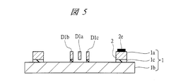
本実施例1における慣性センサについて図面を参照しながら説明する。図4は、本実施例1における慣性センサの主要な構成の一例を示す平面図である。図5は、図4のA-A’線で切断した断面を示す断面図である。
まず、本実施例1における慣性センサの主要な構成(機械構造部)について説明する。図4および図5において、慣性センサS2は、例えば、SOI(Silicon On Insulator)基板1をフォトリソグラフィとDRIE(Deep Reactive Ion Etching)を用いて加工することで形成する場合を想定している。勿論ここではSOI基板1を使って製作する例を説明しているだけであって、本発明の概念はガラス・シリコン・ガラスの接合技術などのシリコン基板の表・裏面を加工することで構造を形成する所謂バルクMEMSプロセスを用いて製作してもよく、または、予めトランジスタなどの信号処理用の回路が形成されているシリコン基板の表面に薄膜を堆積し、堆積した薄膜をパターニングすることを繰り返すことで構造を形成する所謂表面MEMSプロセスを用いて製作してもよい。
ここで例として挙げているSOI基板1は、支持基板1b上に中間絶縁層1cが形成されており、この中間絶縁層1c上に活性層(導体層)1aが形成されている。支持基板1bは、例えば、シリコン(Si)より形成され、中間絶縁層1cは、例えば、酸化シリコン(SiO2)より形成されている。さらに、中間絶縁層1c上に形成されている活性層1aは、例えば、導電性シリコンより形成されている。
本実施例1の慣性センサS2は、前記支持基板1bに前記中間絶縁層1cを介して支持固定されている固定部2と、この固定部2に後述する可動部6を可動状態に支えている支持梁3と、この支持梁3に懸架され、加速度が印加された際にその加速度に追従して変位する可動部6と、この可動部6の変位量を検出するための検出部D1,D2と、ワイヤボンディング等により外部回路と信号のやり取りを行うための電極パッド2e,D1be,D1ce,D2be,D2ceとで構成されている。
前記検出部D1は、可動電極D1aと固定電極D1b,D1cが並行平板状に配置され、夫々静電容量C1,C2を形成している。同様に、前記検出部D2は、可動電極D2aと固定電極D2b,D2cが並行平板状に配置され、夫々静電容量C3,C4を形成している。夫々の検出部D1,D2は差動検出ができるように構成され、例えば、検出部D1には可動部6が+x方向に変位した場合、静電容量が減少する静電容量C1と静電容量が増加する静電容量C2で構成される。同様に、検出部D2には可動部6が+x方向に変位した場合、静電容量が減少する静電容量C3と静電容量が増加する静電容量C4で構成される。これらの検出部D1,D2は、印加された加速度の慣性力と各検出部から発生する物理量の比で定義した感度(S)が異なる構成となっている。
この慣性センサS2においては、可動部6をこの可動部6から4方向に延びる支持梁3で可動可能にSOI基板1に固定する4箇所の固定部2のうちの一つの固定部2の表面上に電極パッド2eが設けられている。なお、4箇所の固定部2に設けることも可能である。また、前記検出部D1の夫々の固定電極D1b,D1cの外側端部の表面上に電極パッドD1be,D1ceが設けられている。同様に、前記検出部D2の夫々の電極パッドD2b,D2cの外側端部の表面上に電極パッドD2be,D2ceが設けられている。
図6は、本実施例1の慣性センサS2を実装したパッケージ構造の一例を示す断面図である。
本実施例1の慣性センサS2を実装したパッケージ構造は、セラミックPKG(パッケージ)200を用いている。まず、セラミックPKG200の凹部の内側底面に、接着剤50を介して、後述する図9に示すセンサ制御・信号処理用IC100を実装する。さらに、センサ制御・信号処理用IC100の上に、再び接着剤50を介して前記慣性センサS2を実装する。その後、前記センサ制御・信号処理用IC100と前記慣性センサS2間をワイヤボンディングによりワイヤ70で電気的に接続する。最後に、前記センサ制御・信号処理用IC100と前記セラミックPKG200間をワイヤ80で電気的に接続し、蓋60で封止することで、パッケージ構造の慣性センサが完成する。
次に、本実施例1(本発明)の特徴的構成についてさらに詳しく説明する。本発明の特徴は、複数のレンジを一つの振動系で測定するため、夫々のレンジに対応する複数の検出部を持っていることである。ここで、一つの振動系とは一つの可動部と一つのばね(支持梁に相当)で表現できる振動構造を意味する。例えば、前記図4に示している慣性センサS2を、ばね(ばね定数k)、可動部、減衰(c)と、機能説明の便宜上、検出部D1,D2で構成した振動系モデルに書き直せば図7となる。
図7は、本実施例1の慣性センサS2の振動系モデルを示す説明図であり、実際の形状と対応するように同一部材には同一の符号を付している。この振動系モデルにおいて、主に前記可動部6と前記可動電極D1a,D2aの質量が前記式(1)のmとなり、前記支持梁3のばね定数の合計がkとなる。従って、前記式(1)より前記慣性センサS2の固有振動数f0と、検出方向(x方向)に加速度aが印加された場合の前記可動部6の変位xの変位量を求めることができる。
変位xが発生すると、前記検出部D1とD2の夫々の、可動電極D1aと固定電極D1b,D1c間、可動電極D2aと固定電極D2b,D2c間の間隔が変動し、前記検出部D1の静電容量C1,C2、前記検出部D2の静電容量C3,C4は夫々変化する。この静電容量の変化は、後述する図9に示すセンサ制御・信号処理用IC100で検出することができる。すなわち、静電容量の変化は、センサ制御・信号処理用IC100から静電容量を検出するための搬送波101を前記検出部D1の電極パッドD1be,D1ce、前記検出部D2の電極パッドD2be,D2ceに印加することで、前記可動部6に連結されている電極パッド(共通電極)2eを介して前記センサ制御・信号処理用IC100のCV変換部102に差動入力される。このCV変換部102で、静電容量の変化は電圧信号に変換され、さらに同期検波回路103で必要な信号成分のみを取り出し、最後にA/D変換部104でデジタル値に変換した後、外部に出力する。
次に、前記検出部D1,D2の設計に関してより詳しく説明する。ここでは、説明の便宜上、具体的な数値を用いるが、特に本実施例1(本発明)の効果を限定しているわけではなく、本発明の概念は一般的に適用可能である。
例えば、加速度範囲±2Gと±4Gを±1%の検出非線形性で検出する加速度センサを想定する。そして、前記センサ制御・信号処理用IC100のCV変換部102が飽和する静電容量変化(ΔC)の入力を0.25pFとし、前記複数の検出部D1,D2の中で検出部D1の可動電極D1aと固定電極D1b,D1c間の間隔gを3μmとする。ここで、間隔gは、プロセス的な制約により決まる場合が多い。並行平板型の静電容量検出方式の検出部の場合、その初期容量は静電容量を形成する両電極の対抗面積Aに比例し、両電極間の間隔gに反比例する。そのため、間隔gを狭く形成するほど、対抗面積Aを小さくすることができ、結果的に小型化になる。
以上で、設計に必要な前提条件もしくは仕様が揃ったので、本実施例1(本発明)の概念に基づき慣性センサS2の固有振動数f0ともう一つの検出部D2を設計すればよい。まず、固有振動数f0は検出部D1,D2の中で間隔gが狭い方(ここでは、検出部D1の間隔3μm)と非線形性仕様±1%により決まる。図8は、前記図3の一部を拡大した図に可動部6の変位xにおける検出非線形性を上乗せしたものである。すなわち、図8は、変位xに対する非線形性NLと静電容量変化ΔCを示すグラフである。
ここで、非線形性NLの定義は、変位xが0の時の検出部の容量変化率、つまり、前記式(2)を変位xに対して微分した式に変位xとして0を代入して得られる値(感度S)に変位xを掛けた理想的な容量変化直線に対して、実際に変位xによって得られる静電容量変化ΔCの比である。下記の式(4)に感度Sの定義を示し、式(5)に非線形性NLの定義を示す。

式(4)において、
S:慣性センサの感度(x=0)
を示す。
S:慣性センサの感度(x=0)
を示す。

式(5)において、
S(0):慣性センサの感度
x:可動部6の変位
を示す。
S(0):慣性センサの感度
x:可動部6の変位
を示す。
図8から、前記検出部D1の間隔gが3μmの場合、非線形性NLが±1%以下を満足する変位xは±0.3μmであることがわかる。これは、検出部D1を用いて出力の非線形性が±1%を満足しながら最大のSNRを得るためには加速度測定範囲である±2Gで可動部6を±0.3μm変位させる必要があることを意味する。勿論、信号成分以外の振動外乱等の影響により想定した静電容量変化ΔCより大きいΔCが発生するため、実際の設計時には非線形性にマージンを持った設計をする必要があるが、これは、本発明の本質とは関係がないために説明は省略する。しかし、この場合でも、本発明の基本概念は適用可能である。ここでは、信号成分以外の振動外乱等はないものと仮定し、説明を続ける。
必要な変位量が決まれば、前記式(1)の変位xと固有振動数f0の関係式から固有振動数f0が決まる。ここで例として説明している慣性センサS2の場合、固有振動数f0は1300Hzとなる。
次に、前記検出部D2の設計について説明する。検出部D2で検出非線形性が±1%以下を満足しながら最大のSNRを得るためには、加速度範囲が±4Gを検出非線形性NLが±1%で検出できればよい。本慣性センサS2の固有振動数f0は1300Hzであるため、±4G印加時の変位xは、前記式(1)から±0.6μmになる。従って、変位xが±0.6μmになった場合、非線形性NLが±1%になる検出部D2の可動電極D2aと固定電極D2b,D2c間の間隔gを決めればよく、本慣性センサS2では、6μmとなる(図8参照)。
しかし、ただ単に間隔だけを広くしただけでは、前記検出部D2の初期静電容量C3,C4も小さくなるため、±4G印加時のΔCの絶対値も小さくなる。慣性センサS2の場合、±2G印加時の検出部D1の静電容量変化ΔCと±4G印加時の検出部D2の静電容量変化ΔCとの比は7.43となる。従って、検出部D2の電極規模を検出部D1の7.43倍にしてあげることで、CV変換部102を共有することができる。ここでは、電極間の対抗面積Aを大きくすることで、検出部D2の規模を大きくしている。結果的に、検出部D1とD2は両方とも最大測定加速度(±2Gと±4G)に対して同じ静電容量変化ΔCとなる。すなわち、各検出部D1,D2の測定レンジごとに測定可能な最大加速度が印加された場合の静電容量の変化値が同じ値である。
図9は、本実施例1における慣性センサS2の電気的構成の一例を示す構成図である。図9では、各レンジの選択と選択されていない検出部の処理方法を説明する。
本実施例1の慣性センサS2は、電気的構成において、前述したような検出部D1,D2と可動部6などからなる機械構造部に接続されるセンサ制御・信号処理用IC100と、切換スイッチモニタ107などから構成され、また外部入力108が可能となっている。センサ制御・信号処理用IC100には、検出部D1,D2の静電容量の変化値を電圧値に変換するCV変換部102、CV変換部102からの出力を同期検波する同期検波回路103、同期検波回路103からの出力をアナログ/デジタル変換するA/D変換部104、CV変換部102からの出力値(具体的には同期検波およびアナログ/デジタル変換した後のA/D変換部104の出力値)が一定範囲を超えているかどうかを判断するオーバーレンジ判断部105、オーバーレンジ判断部105からの出力信号に基づいて検出部D1,D2に印加する搬送波101と検出部D1,D2からの信号とを切換えるレンジ切換スイッチ106などが設けられ、また、レンジ切換スイッチ106は、測定レンジのいずれかを選択するスイッチとしても機能している。
本実施例1の慣性センサS2は、手動で測定レンジを切換える方法と、自動で測定レンジを切換える方法に対応できる。
まず、自動で測定レンジを切換える方法から説明する。慣性センサS2の初期状態として、図9のレンジ切換スイッチ106はステート1に設定され、前記検出部D1(±2Gレンジ)に前記搬送波101が印加される。一方、前記検出部D2はコモン電位に接続され、可動部6のDCレベルと同じ電位となる。この状態で、±2G以上の加速度が印加されると、前記CV変換部102が飽和するか、もしくはA/D変換部104の出力端の電圧は一定値を超えることとなる。
加速度が印加されると、可動部6は慣性の法則に従い加速度とは逆の方向に変位する。この時の検出部D1の可動電極D1aと固定電極D1b,D1c間、検出部D2の可動電極D2aと固定電極D2b,D2c間の静電容量の変化を、CV変換部102によって電圧値の変化に変換し、さらに同期検波回路103で同期検波した後に、A/D変換部104によってアナログ値をデジタル値に変換する。
そして、オーバーレンジ判断部105は、前記A/D変換部104からの出力値に基づきオーバーレンジか否かを判断し、オーバーレンジの場合(yes)には、前記レンジ切換スイッチ106の状態を制御する信号を生成し、レンジ切換スイッチ106を切換えることでより広い測定レンジ(ステート1からステート2)に切換える。一方、オーバーレンジでない場合(no)は、広い測定レンジに切換える必要がないので、ステート1のままとなる。また、前記レンジ切換スイッチ106は現在の状態を外部の切換スイッチモニタ107に出力することで、選択されている測定レンジを外部に通知する。
一方、手動で測定レンジを切換える方法では、外部入力108により、レンジ切換スイッチ106をステート1からステート2に切換える。
本実施例1の慣性センサS2では、±2Gと±4Gの測定レンジが選択できる。また、測定レンジは、前記慣性センサS2の固有振動数f0と前記検出部D1とD2の中で可動電極と固定電極間の間隔が狭い方の間隔によって制限されるのであって、特に、±2Gと±4Gに限定しているわけではない。例えば、本実施例1の慣性センサS2の場合、前記検出部D1の可動電極D1aと固定電極D1b,D1cの間隔が3μmであり、前記式(1)から20Gの加速度が印加された場合に前記検出部D1の可動電極D1aと固定電極D1b,D1cが物理的に接触する。従って、前記慣性センサS2の測定限界は20Gとなる。
しかし、より広範囲の加速度を測定したい場合には前記固有振動数f0を高くすればよい。前記式(1)の関係から、固有振動数f0を5倍高くすれば、測定可能なレンジは25倍となる。つまり、f0が1300Hzの場合に±2Gと±4Gだった出力レンジがf0を6500Hzにすることで、±50Gと±100Gとなる。また、感度Sが異なる検出部を増設することで、選択できる測定レンジも増える。
以上説明した本実施例1における慣性センサS2の設計の手順を実施することで、全ての測定レンジにおいて、最大のSNRと規定値以下の加速度出力線形性が確保できる慣性センサを提供することができる。すなわち、印加された加速度と検出部から発生する物理量の比で定義した感度(S:式(4))が異なる複数の検出部D1,D2によって複数のレンジ出力が得られ、全ての測定レンジにおいて、SNRと加速度出力の線形性向上を両立させることができる。
本実施例2における慣性センサの最大の特徴は、大きく異なる二つの測定レンジを持つことである。前記実施例1で説明した慣性センサは、複数のレンジを持つものの、現実的に一緒に製作可能な前記電極間の間隔gと、機械構造の大きさの制限から、各レンジ間の比は5以下が現実的であろう。
本実施例2における慣性センサは、複数の可動部と、各可動部の固定部に対する相対変位を検出する検出部と、各可動部間の相対変位を検出する検出部(少なくとも1個)を備えることで、複数の出力レンジを持ちながらも、測定レンジ間の比が10以上であることを特徴とする。さらに、夫々の検出部は互いにその間隔などの形状が類似しているため、加工誤差による性能バラツキが少なく、加工誤差にロバストである。
以下に、本実施例2における慣性センサについて図面を参照しながら説明するが、前記実施例1と重複するところは同一の符号を付し、説明は省略する。図10は、本実施例2における慣性センサの主要な構成の一例を示す平面図である。
本実施例2の慣性センサS3は、支持基板1bに支持固定されている固定部2a,2b,2cと、この固定部2a,2b,2cの夫々に後述する可動部6a,6b,6cを可動状態に支えている支持梁3a,3b,3cと、この支持梁3a,3b,3cの夫々に懸架され、加速度が印加された際にその加速度に追従して変位する可動部6a,6b,6cと、この可動部6a,6b,6cの変位量を検出するための検出部D1,D2,D3,D4と、ワイヤボンディング等により外部回路と信号のやり取りを行うための電極パッド(符号省略)とで構成されている。
前記検出部D1は、可動部6aの固定部2aに対する相対変位を検出する検出部であり、可動電極D1aと固定電極D1b,D1cが並行平板状に配置されている。前記検出部D2は、可動部6aと可動部6b,6c間の相対変位を検出する検出部であり、一方の可動電極D2aと固定電極D2b、他方の可動電極D2aと固定電極D2cの夫々が並行平板状に配置されている。また、前記検出部D3は、前記検出部D1と同様に、可動部6bの固定部2bに対する相対変位を検出する検出部であり、可動電極D3aと固定電極D3b,D3cが並行平板状に配置されている。前記検出部D4も、可動部6cの固定部2cに対する相対変位を検出する検出部であり、可動電極D4aと固定電極D4b,D4cが並行平板状に配置されている。
本実施例2の慣性センサS3の製造プロセスや実装形態などは前記実施例1と同じであるために説明を省略し、本実施例2の特徴である、大きく異なる測定レンジがなぜ可能であるのかと、なぜ間隔などの形状が類似した検出部で実現することができるのかを詳細に説明する。ここでも、前記実施例1と同様に限定するわけではないが、説明の便宜上、±2Gと±100Gの具体的な測定レンジを例として説明する。
図10を振動系モデルとして書き直せば図11となる。図11は、本実施例2の慣性センサS3の振動系モデルを示す説明図であり、実際の形状と対応するように同一部材には同一の符号を付している。本実施例2の慣性センサS3は、三つの振動系として構成される。第1の振動系は可動部6aとばね(支持梁3a)、検出部D1,D2とで構成され、第2の振動系は可動部6bとばね(支持梁3b)、検出部D2,D3で構成され、第3の振動系は可動部6cとばね(支持梁3c)、検出部D2,D4とで構成される。前記第1の振動系の変位x1を狭い測定レンジ(例えば、±2G)の検出に用いる。また、前記第2と第3の振動系は同じ固有振動数f2=f3を持つように形成されているため、前記式(1)からその単位加速度当たりの変位x2,x3もx2=x3になる。本実施例2の慣性センサS3では、前記変位x1とx2もしくはx3との変位差を用いて広い測定レンジ(例えば、±100G)の測定を行う。つまり、本実施例2の最大の特徴は複数の可動部6a,6b間の相対変位(変位差)を用いることで広い測定レンジを測定していることである。
次に、本実施例2の慣性センサS3の設計と機能に関して説明する。本実施例2でも前記実施例1と同様、センサ制御・信号処理用IC100のCV変換部102(後述する図12参照)が飽和する静電容量変化(ΔC)の入力を0.25pFとし、プロセス的な制約から検出部の可動電極と固定電極間の間隔gを3μmとする。また、出力非線形性も±1%以下とする。本慣性センサS3は、±100Gの加速度を検出するため、±100Gの加速度が印加されても全ての検出部D1,D2,D3,D4を構成する可動電極D1a,D2a,D3a,D4aと固定電極D1b,D1c,D2b,D2c,D3b,D3c,D4b,D4cが物理的に接触しないように第1から第3の各振動系の固有振動数f1,f2,f3を設計する必要がある。
前記式(1)から、±100Gの加速度が印加された場合、変位xが3μmとなる固有振動数は2877Hzであり、本実施例2の慣性センサS3では前記第1の振動系の固有振動数f1を3000Hzに設定している。固有振動数f1を3000Hzにしたため、第1の振動系の可動部6aの±2G印加時の変位量x1は55nmとなり、図8で示しているように300nm以下であるために非線形性が±1%以下を満足する。しかし、静電容量変化ΔCを0.25pFとするためには、前記実施例1の慣性センサS2の検出部の5.3倍の電極規模が必要となる。活性層1aの厚さなどによって変わるが、本実施例2の慣性センサS3では、活性層1aの厚さは40μmであり、検出部D1の可動電極D1aと固定電極D1b,D1cとのオーバーラップを200μmにしているため、電極の本数を140本としている。前記検出部D1は並行平板型の静電容量検出方式であり、可動電極と固定電極を構成している櫛歯の幅を4μmとすると、検出部D1を形成するために必要な長さは2940μmとなり、可動部6aの両側に電極を形成しているため、第1の振動系は概ね1.5mm×1.5mmの大きさになる。慣性センサの大きさは前記検出部D1の間隔gと前記活性層1aの厚さの比として定義されるアスペクト比が大きくできれば、もっと小型にすることができる。
次に、前記第2と第3の振動系の固有振動数f2,f3について説明する。固有振動数f2とf3は±100G印加時に可動部6aと6bもしくは6c間の相対変位が、非線形性が±1%以下を満足しながら電極の規模をなるべく小さくするために、300nmになるように設計すればよい。前記式(1)から固有振動数f2とf3を3178Hzにすれば、±100G印加時の可動部6aと6bもしくは6cとの相対変位(x1-x2もしくはx1-x3)は300nmとなり、非線形性が±1%以下の仕様を満足しながらも検出部D1のおおよそ5.3分の1の電極規模で静電容量変化ΔCが0.25pFとなる検出部D2を形成することができる。
ここでは、前記第1の振動系の固有振動数f1を3000Hzとし、前記第2と第3の振動系の固有振動数f2,f3を3178Hzとしているが、その逆である前記固有振動数f1を3178Hzとし、前記固有振動数f2,f3を3000Hzにしても構わない。この場合は、電極規模が大きい検出部D1を慣性センサS3の外回りに配置することができるため、小型化に有利となる。
次に、検出部(固有振動数調整部の機能も具備、以下において固有振動数調整部と記載する)D3,D4について、後述する図12を参照しながら説明する。本実施例2の慣性センサS3では、前記固有振動数調整部D3,D4の可動電極D3a,D4aと固定電極D3b,D3c,D4b,D4cの間にDC電圧を印加することで、既に公知である静電ばね効果を用いて前記可動部6bと6cを含む前記第2と第3の振動系の固有振動数f2,f3を調整している。
上述したように、±100Gの測定には可動部6aと可動部6b,6cとの相対変位を用いている。従って、可動部6bと6cは単位加速度当たりの変位量が同じである必要がある。しかし、可動部6bと6cを含む第2と第3の振動系は場所的に離れ、独立した振動系として構成されているため、加工誤差の影響から各振動系の固有振動数をぴったり一致させることはほぼ不可能に近い。従って、固有振動数調整部D3,D4を設けることによって、第2と第3の振動系の固有振動数f2,f3を調整している。具体的には出荷時に前記慣性センサS3をAC的に加振し、慣性センサS3のDCレベル出力が0となるように固有振動数調整部D3,D4に印加するDC電圧109,110を調整する(図12参照)。
前記固有振動数調整部D3,D4は前記検出部D1と同じ構成となっているため、可動部6b,6cの変位x2,x3を検出するために用いることも可能である。特に、各測定レンジ間の比が小さい慣性センサでは、第1の振動系の固有振動数f1と第2と第3の振動系の固有振動数f2,f3間の固有振動数の差は大きくなるため、加工誤差による固有振動数のずれはほぼ無視でき、固有振動数調整部D3,D4を検出部として転用することで測定レンジ数を増やすことができる。
図12は、本実施例2の慣性センサS3における電気的構成であり、夫々、前記D3,D4を固有振動数調整部として使った場合を示す。図示はしないが、前記固有振動数調整部D3,D4を、可動部6bと6cの変位x2,x3を検出する検出部として使う場合は、搬送波101を固有振動数調整部D3,D4に印加すればよい。
本実施例2でも、前記実施例1の慣性センサS2と同様、前記測定レンジは外部入力108を通じて手動で切換えることもできれば、オーバーレンジ判断部105を通じて自動で切換えることもできる。この測定レンジを切換える具体的な内容としては前記実施例1の慣性センサS2と同じであるため、説明は省略する。
以上説明した本実施例2における慣性センサS3の設計の手順を実施することで、大きく異なる(±2Gと±100G)測定レンジを持ちながらも、加工バラツキにロバストな慣性センサを提供することができる。すなわち、夫々の検出部D1,D2,D3,D4は互いにその間隔などの形状が類似し、各振動系を構成する可動部6a,6b,6cとばね(支持梁3a,3b,3c)の形状をほぼ同じにできるので、加工誤差による性能バラツキへの影響は比較的に小さく、加工誤差にロバストとなり、また小型化を実現することができる。
本実施例3は複数の測定レンジを持つ慣性センサであり、複数の可動部とばねで構成する複数の振動系が互いに連結され、夫々の振動系の可動部の基板に対する絶対変位と、各可動部間の相対変位を測定することで振動系の数+1以上の測定レンジを持つことと、各振動系は互いに可動部とばねを共有するため、小型化に有利であることが特徴である。以下に、図面を参照しながら本実施例3を詳細に説明する。また、前記実施例1,2と重複する部分については同じ符号を付し、説明は省略する。
図13は、本実施例3における慣性センサの主要な構成の一例を示す平面図である。本実施例3の慣性センサS4は、支持基板1bに支持固定されている固定部2a,2b,2cと、この固定部2a,2b,2cに後述する可動部6bを可動状態に支えている支持梁3bと、この支持梁3bに懸架され、加速度が印加された際にその加速度に追従して変位する可動部6bと、この可動部6bに後述する可動部6aを可動状態に支えている支持梁3aと、この支持梁3aに懸架され、加速度が印加された際にその加速度に追従して変位する可動部6aと、可動部6a,6bの変位量を検出するための検出部D1,D2,D3と、ワイヤボンディング等により外部回路と信号のやり取りを行うための電極パッド(符号省略)とで構成されている。
前記検出部D1は、一方の可動電極D1aと固定電極D1b、他方の可動電極D1aと固定電極D1cの夫々が並行平板状に配置されている。同様に、前記検出部D2は、一方の可動電極D2aと固定電極D2b、他方の可動電極D2aと固定電極D2cの夫々、前記検出部D3は、一方の可動電極D3aと固定電極D3b、他方の可動電極D3aと固定電極D3cの夫々、が並行平板状に配置されている。
本実施例3の慣性センサS4は、二つの振動系として構成される慣性センサを示している。勿論、二つの振動系に限定するわけではなく、N個の振動系として構成してもよい。また、N個の振動系として構成した場合の測定レンジはN+1個以上となる。
図13を振動系モデルとして書き直せば図14となる。図14は、本実施例3の慣性センサS4の振動系モデルを示す説明図であり、実際の形状と対応するように同一部材には同一の符号を付している。本実施例3の慣性センサS4は、可動部6a(可動部m1)とばね(支持梁3a)となる第1の振動系と、可動部6b(可動部m2)とばね(支持梁3b)となる第2の振動系として構成される。特に、前記第2の振動系は前記可動部6bが絶縁物質となる絶縁膜7により3等分され、夫々の可動部6b1,6b2,6b3は機械的には接続され、電気的には分離されている。
前記絶縁膜7は活性層1aをDRIEで深堀し、厚膜CVD(Chemical Vapor Deposition)等により酸化膜などの絶縁膜を埋め込むことにより形成される。さらに、前記絶縁膜7は可動部6b1,6b2,6b3同士が絶縁膜7の界面で壁壊することを防ぐため、図13に示しているように少なくとも1回(図13では4回の例)は折り曲がった形状として形成されている。
本実施例3の慣性センサS4の測定レンジは、第1の可動部6aの変位x1と、第2の可動部6bの変位x2と、可動部6a,6bの相対変位xrを測定することで、三つを選択することができる。本実施例の慣性センサS4は、数kHz帯域に二つの可動部6a,6bが同位相で振動する第1モード固有振動数を持つ。加速度センサは主に数10~100Hz以下の周波数成分を測定する場合が多く、可動部6a,6bの変位の位相差は発生せず、可動部6aの支持基板1bに対する変位x1は可動部6bの変位x2と可動部6aと6bの相対変位xrの和となる。従って、すべての加速度の印加に対してx1>x2の関係となる。
前記変位量x1,x2,xrは前記式(1)を使うことで求めることができる。まず、可動部6aと6bの相対変位xrは、図14で示している振動系モデルを二つの独立した1自由度系として見なした場合、可動部6aと検出部D1とD2の可動電極D1a,D2aの質量をmとし、可動部6aを支持している支持梁3aのばね定数をkとすることで求められる第1の固有振動数f1を前記式(1)に代入することで求められる。
次に、変位量x2は、可動部6bの変位であり、可動部6bとこの可動部6bに接続されて宙づりになっている支持梁3a、可動部6a、検出部D1の可動電極D1a、検出部D2の可動電極D2aの質量をmとし、可動部6bを支持している支持梁3bのばね定数をkとすることで求められる第2の固有振動数f2を前記式(1)に代入することで求められる。また、可動部6aの支持基板1bに対する変位x1は変位x2とxrの和として求めることができる。以上の変位x1,xr,x2を夫々検出部D1,D2,D3を用いて検出することで、三つの測定レンジが得られる。
図15は、本実施例3の慣性センサS4における電気的構成であり、前記三つの測定レンジはオーバーレンジ判断部105と、レンジ切換スイッチ106、外部入力108を用いることで、自動もしくは手動で切換えることができる。ここでは、前記実施例1の慣性センサS2と異なる内容を主として説明する。
レンジ切換スイッチ106は、測定レンジに合わせて三つのステートを持っている。まず、ステート1は、可動部6b2を介して可動部6aに搬送波101を印加し、検出部D1の固定電極D1b,D1cからの出力をCV変換部102に入力することで、可動部6aの変位x1を検出する。この際、他の検出部D2,D3と可動部6b1,6b3はCV変換部102のDCバイアスに接続される。
次に、ステート2は、前記ステート1と同様に可動部6b2を介して可動部6aに搬送波101を印加し、検出部D2の固定電極D2b,D2cからの出力を夫々可動部6b1と6b2を介してCV変換部102に入力することで、可動部6aと6bの相対変位xrを検出する。この際、他の検出部D1とD3はCV変換部102のDCバイアスに接続される。
最後に、ステート3は、搬送波101を可動部6b1,6b3に印加し、検出部(固有振動数調整部)D3の固定電極D3b,D3cからの出力をCV変換部102に入力することで、可動部6bの変位x2を検出する。この際、可動部6b2とその他の検出部D1はCV変換部102のDCバイアスに接続される。
以上説明した本実施例3における慣性センサS4によれば、二つの振動系で三つの測定レンジを得ることができるように、N個の振動系を持ちながらも各振動系間の相対変位を測定することで、少なくともN+1個の測定レンジが得られる。すなわち、可動部6a,6bとばね(支持梁3a,3b)とで構成される振動系の数より多い出力レンジを得ることができる。
以上、本発明者によってなされた発明を実施例に基づき具体的に説明したが、本発明は前記実施例に限定されるものではなく、その要旨を逸脱しない範囲で種々変更可能であることはいうまでもない。
本発明による慣性センサは、自動車、携帯用機器、アミューズメント機器、情報家電など、極めて多岐にわたって利用可能である。
1 SOI基板
1a 活性層
1b 支持基板
1c 中間絶縁層
2,2a,2b,2c 固定部
2e 電極パッド
3,3a,3b,3c 支持梁
6,6a,6b,6c 可動部
7 絶縁膜
50 接着剤
60 蓋
70,80 ワイヤ
100 センサ制御・信号処理用IC
101 搬送波
102 CV変換部
103 同期検波回路
104 A/D変換部
105 オーバーレンジ判断部
106 レンジ切換スイッチ
107 切換スイッチモニタ
108 外部入力
109,110 DC電圧
200 セラミックPKG
D1,D2,D3,D4 検出部
D1a,D2a,D3a,D4a 可動電極
D1b,D1c,D2b,D2c,D3b,D3c,D4b,D4c 固定電極
D1be,D1ce,D2be,D2ce 電極パッド
S1 加速度センサ
S2,S3,S4 慣性センサ
Claims (16)
- 基板上に弾性体を介して懸架された可動部と、
前記可動部に形成された可動電極と前記基板上に設けられた固定電極とで構成される複数の検出部と、を備え、
前記複数の検出部の静電容量の変化に基づいて加速度の慣性力を検出する慣性センサであって、
前記複数の検出部は、印加された慣性力と各検出部から発生する物理量との比で定義した感度が異なり、
複数の測定レンジを有することを特徴とする慣性センサ。 - 請求項1記載の慣性センサにおいて、
前記複数の検出部は、並行平板型の静電容量検出方式であり、各検出部の測定レンジごとに測定可能な最大加速度が印加された場合の静電容量の変化値が同じ値であることを特徴とする慣性センサ。 - 請求項1記載の慣性センサにおいて、さらに、
前記複数の測定レンジのいずれかを選択するスイッチを備えていることを特徴とする慣性センサ。 - 請求項1記載の慣性センサにおいて、さらに、
前記複数の検出部の静電容量の変化値を電圧値に変換する変換部と、
前記変換部からの出力値が一定範囲を超えているかどうかを判断する判断部と、
前記判断部からの出力信号に基づいて前記複数の検出部に印加する搬送波と前記複数の検出部からの信号とを切換えるスイッチと、を備えていることを特徴とする慣性センサ。 - 基板上の固定部に弾性体を介して接続されたN(2以上の自然数)個の可動部と、
前記N個の各可動部の前記固定部に対する相対変位を検出する複数の第1の検出部と、
前記各可動部間の相対変位を検出する少なくとも1個の第2の検出部と、を備え、
(N+1)個以上の測定レンジを有することを特徴とする慣性センサ。 - 請求項5記載の慣性センサにおいて、
前記(N+1)個以上の測定レンジは、測定レンジ間の比が10以上であることを特徴とする慣性センサ。 - 請求項5記載の慣性センサにおいて、
前記複数の第1の検出部および前記少なくとも1個の第2の検出部は、並行平板型の静電容量検出方式であり、各検出部の測定レンジごとに測定可能な最大加速度が印加された場合の静電容量の変化値が同じ値であることを特徴とする慣性センサ。 - 請求項5記載の慣性センサにおいて、さらに、
前記(N+1)個以上の測定レンジのいずれかを選択するスイッチを備えていることを特徴とする慣性センサ。 - 請求項5記載の慣性センサにおいて、さらに、
前記複数の第1の検出部および前記少なくとも1個の第2の検出部の静電容量の変化値を電圧値に変換する変換部と、
前記変換部からの出力値が一定範囲を超えているかどうかを判断する判断部と、
前記判断部からの出力信号に基づいて前記複数の第1の検出部および前記少なくとも1個の第2の検出部に印加する搬送波と前記複数の第1の検出部および前記少なくとも1個の第2の検出部からの信号とを切換えるスイッチと、を備えていることを特徴とする慣性センサ。 - 基板上の固定部に第1の弾性体を介して接続された第1の可動部と、前記第1の可動部に第2の弾性体を介して接続された第2の可動部とを少なくとも含むN(2以上の自然数)個の可動部と、
前記N個の各可動部の前記固定部に対する相対変位を検出する複数の第1の検出部と、
前記各可動部間の相対変位を検出する少なくとも1個の第2の検出部と、を備え、
(N+1)個以上の測定レンジを有することを特徴とする慣性センサ。 - 請求項10記載の慣性センサにおいて、
前記第1の可動部は、機械的には連結され、電気的には絶縁膜を挟むことで分離されていることを特徴とする慣性センサ。 - 請求項11記載の慣性センサにおいて、
前記絶縁膜は、少なくとも1回は折り曲がっていることを特徴とする慣性センサ。 - 請求項10記載の慣性センサにおいて、
前記(N+1)個以上の測定レンジは、測定レンジ間の比が10以上であることを特徴とする慣性センサ。 - 請求項10記載の慣性センサにおいて、
前記複数の第1の検出部および前記少なくとも1個の第2の検出部は、並行平板型の静電容量検出方式であり、各検出部の測定レンジごとに測定可能な最大加速度が印加された場合の静電容量の変化値が同じ値であることを特徴とする慣性センサ。 - 請求項10記載の慣性センサにおいて、さらに、
前記(N+1)個以上の測定レンジのいずれかを選択するスイッチを備えていることを特徴とする慣性センサ。 - 請求項10記載の慣性センサにおいて、さらに、
前記複数の第1の検出部および前記少なくとも1個の第2の検出部の静電容量の変化値を電圧値に変換する変換部と、
前記変換部からの出力値が一定範囲を超えているかどうかを判断する判断部と、
前記判断部からの出力信号に基づいて前記複数の第1の検出部および前記少なくとも1個の第2の検出部に印加する搬送波と前記複数の第1の検出部および前記少なくとも1個の第2の検出部からの信号とを切換えるスイッチと、を備えていることを特徴とする慣性センサ。
Priority Applications (3)
| Application Number | Priority Date | Filing Date | Title |
|---|---|---|---|
| JP2010527740A JPWO2010026843A1 (ja) | 2008-09-08 | 2009-07-28 | 慣性センサ |
| EP09811372.3A EP2336788B1 (en) | 2008-09-08 | 2009-07-28 | Inertial sensor |
| US13/058,571 US20110132089A1 (en) | 2008-09-08 | 2009-07-28 | Inertial Sensor |
Applications Claiming Priority (2)
| Application Number | Priority Date | Filing Date | Title |
|---|---|---|---|
| JP2008-229535 | 2008-09-08 | ||
| JP2008229535 | 2008-09-08 |
Publications (1)
| Publication Number | Publication Date |
|---|---|
| WO2010026843A1 true WO2010026843A1 (ja) | 2010-03-11 |
Family
ID=41797015
Family Applications (1)
| Application Number | Title | Priority Date | Filing Date |
|---|---|---|---|
| PCT/JP2009/063421 WO2010026843A1 (ja) | 2008-09-08 | 2009-07-28 | 慣性センサ |
Country Status (4)
| Country | Link |
|---|---|
| US (1) | US20110132089A1 (ja) |
| EP (1) | EP2336788B1 (ja) |
| JP (1) | JPWO2010026843A1 (ja) |
| WO (1) | WO2010026843A1 (ja) |
Cited By (10)
| Publication number | Priority date | Publication date | Assignee | Title |
|---|---|---|---|---|
| JP2012002560A (ja) * | 2010-06-15 | 2012-01-05 | Denso Corp | 力学量センサ |
| US20120036915A1 (en) * | 2010-08-12 | 2012-02-16 | Axel Franke | Sensor system and method for calibrating a sensor system |
| JP2012078337A (ja) * | 2010-09-08 | 2012-04-19 | Denso Corp | 容量式物理量検出装置 |
| US20120188237A1 (en) * | 2009-06-25 | 2012-07-26 | Samsung Electronics Co., Ltd. | Virtual world processing device and method |
| JP2013024683A (ja) * | 2011-07-20 | 2013-02-04 | Mitsubishi Electric Corp | 加速度センサ |
| JP2013076610A (ja) * | 2011-09-30 | 2013-04-25 | Akebono Brake Ind Co Ltd | 加速度センサ回路 |
| JP2013152111A (ja) * | 2012-01-24 | 2013-08-08 | Mitsubishi Electric Corp | 加速度センサ |
| CN108169515A (zh) * | 2016-12-07 | 2018-06-15 | 精工爱普生株式会社 | 物理量传感器、物理量传感器装置、电子设备及移动体 |
| WO2021246107A1 (ja) * | 2020-06-05 | 2021-12-09 | ソニーグループ株式会社 | 固体撮像装置、固体撮像装置の制御方法および移動体 |
| JP7268928B1 (ja) * | 2022-12-02 | 2023-05-08 | 株式会社PetVoice | 呼吸数推定システム、呼吸数推定サーバ、呼吸数推定方法、及び呼吸数推定プログラム |
Families Citing this family (3)
| Publication number | Priority date | Publication date | Assignee | Title |
|---|---|---|---|---|
| JP6160823B2 (ja) * | 2013-09-10 | 2017-07-12 | セイコーエプソン株式会社 | 物理量センサー、振動デバイス、電子機器および移動体 |
| CN112880667B (zh) * | 2019-11-29 | 2023-12-08 | 精工爱普生株式会社 | 传感器单元、电子设备以及移动体 |
| US20230266357A1 (en) | 2022-02-24 | 2023-08-24 | Stmicroelectronics S.R.L. | Micromechanical device for enhanced acceleration measurement |
Citations (6)
| Publication number | Priority date | Publication date | Assignee | Title |
|---|---|---|---|---|
| JP2004198310A (ja) | 2002-12-19 | 2004-07-15 | Tamagawa Seiki Co Ltd | 加速度計の制御方法 |
| JP2004361388A (ja) * | 2003-05-15 | 2004-12-24 | Mitsubishi Electric Corp | 容量型慣性力検出装置 |
| JP2007333467A (ja) * | 2006-06-13 | 2007-12-27 | Hitachi Ltd | 慣性センサ |
| JP2008008820A (ja) | 2006-06-30 | 2008-01-17 | Hitachi Ltd | 慣性センサおよびその製造方法 |
| JP2008070312A (ja) | 2006-09-15 | 2008-03-27 | Hitachi Metals Ltd | マルチレンジ加速度センサー |
| US20080098815A1 (en) * | 2006-10-27 | 2008-05-01 | Stmicroelectronics S.R.L. | Microelectromechanical sensor having multiple full-scale and sensitivity values |
Family Cites Families (9)
| Publication number | Priority date | Publication date | Assignee | Title |
|---|---|---|---|---|
| US5734105A (en) * | 1992-10-13 | 1998-03-31 | Nippondenso Co., Ltd. | Dynamic quantity sensor |
| JPH09113534A (ja) * | 1995-10-23 | 1997-05-02 | Yoshinobu Matsumoto | 加速度センサー |
| JP2000081338A (ja) * | 1999-10-05 | 2000-03-21 | Denso Corp | 力学量センサ |
| JP2002365306A (ja) * | 2001-06-06 | 2002-12-18 | Denso Corp | 力学量センサ |
| GB2393785B (en) * | 2002-10-03 | 2005-08-31 | Toshiba Res Europ Ltd | Method of making a free standing structure |
| JP2004294332A (ja) * | 2003-03-27 | 2004-10-21 | Denso Corp | 半導体力学量センサ |
| JP2006170704A (ja) * | 2004-12-14 | 2006-06-29 | Mitsubishi Electric Corp | 容量型加速度検出装置 |
| US7337671B2 (en) * | 2005-06-03 | 2008-03-04 | Georgia Tech Research Corp. | Capacitive microaccelerometers and fabrication methods |
| TW200813431A (en) * | 2006-08-09 | 2008-03-16 | Hitachi Metals Ltd | Multi-range three-axis acceleration sensor device |
-
2009
- 2009-07-28 JP JP2010527740A patent/JPWO2010026843A1/ja active Pending
- 2009-07-28 WO PCT/JP2009/063421 patent/WO2010026843A1/ja active Application Filing
- 2009-07-28 US US13/058,571 patent/US20110132089A1/en not_active Abandoned
- 2009-07-28 EP EP09811372.3A patent/EP2336788B1/en not_active Not-in-force
Patent Citations (6)
| Publication number | Priority date | Publication date | Assignee | Title |
|---|---|---|---|---|
| JP2004198310A (ja) | 2002-12-19 | 2004-07-15 | Tamagawa Seiki Co Ltd | 加速度計の制御方法 |
| JP2004361388A (ja) * | 2003-05-15 | 2004-12-24 | Mitsubishi Electric Corp | 容量型慣性力検出装置 |
| JP2007333467A (ja) * | 2006-06-13 | 2007-12-27 | Hitachi Ltd | 慣性センサ |
| JP2008008820A (ja) | 2006-06-30 | 2008-01-17 | Hitachi Ltd | 慣性センサおよびその製造方法 |
| JP2008070312A (ja) | 2006-09-15 | 2008-03-27 | Hitachi Metals Ltd | マルチレンジ加速度センサー |
| US20080098815A1 (en) * | 2006-10-27 | 2008-05-01 | Stmicroelectronics S.R.L. | Microelectromechanical sensor having multiple full-scale and sensitivity values |
Non-Patent Citations (1)
| Title |
|---|
| See also references of EP2336788A4 * |
Cited By (15)
| Publication number | Priority date | Publication date | Assignee | Title |
|---|---|---|---|---|
| US20120188237A1 (en) * | 2009-06-25 | 2012-07-26 | Samsung Electronics Co., Ltd. | Virtual world processing device and method |
| US9987553B2 (en) | 2009-06-25 | 2018-06-05 | Samsung Electronics Co., Ltd. | Virtual world processing device and method |
| US9566506B2 (en) * | 2009-06-25 | 2017-02-14 | Samsung Electronics Co., Ltd. | Virtual world processing device and method |
| JP2012002560A (ja) * | 2010-06-15 | 2012-01-05 | Denso Corp | 力学量センサ |
| US20120036915A1 (en) * | 2010-08-12 | 2012-02-16 | Axel Franke | Sensor system and method for calibrating a sensor system |
| DE102010039236B4 (de) | 2010-08-12 | 2023-06-29 | Robert Bosch Gmbh | Sensoranordnung und Verfahren zum Abgleich einer Sensoranordnung |
| US8833135B2 (en) * | 2010-08-12 | 2014-09-16 | Robert Bosch Gmbh | Sensor system and method for calibrating a sensor system |
| JP2012078337A (ja) * | 2010-09-08 | 2012-04-19 | Denso Corp | 容量式物理量検出装置 |
| JP2013024683A (ja) * | 2011-07-20 | 2013-02-04 | Mitsubishi Electric Corp | 加速度センサ |
| US9846176B2 (en) | 2011-09-30 | 2017-12-19 | Akebono Brake Industry Co., Ltd. | Acceleration sensor circuit |
| JP2013076610A (ja) * | 2011-09-30 | 2013-04-25 | Akebono Brake Ind Co Ltd | 加速度センサ回路 |
| JP2013152111A (ja) * | 2012-01-24 | 2013-08-08 | Mitsubishi Electric Corp | 加速度センサ |
| CN108169515A (zh) * | 2016-12-07 | 2018-06-15 | 精工爱普生株式会社 | 物理量传感器、物理量传感器装置、电子设备及移动体 |
| WO2021246107A1 (ja) * | 2020-06-05 | 2021-12-09 | ソニーグループ株式会社 | 固体撮像装置、固体撮像装置の制御方法および移動体 |
| JP7268928B1 (ja) * | 2022-12-02 | 2023-05-08 | 株式会社PetVoice | 呼吸数推定システム、呼吸数推定サーバ、呼吸数推定方法、及び呼吸数推定プログラム |
Also Published As
| Publication number | Publication date |
|---|---|
| EP2336788A4 (en) | 2012-03-14 |
| JPWO2010026843A1 (ja) | 2012-02-02 |
| EP2336788A1 (en) | 2011-06-22 |
| US20110132089A1 (en) | 2011-06-09 |
| EP2336788B1 (en) | 2014-07-09 |
Similar Documents
| Publication | Publication Date | Title |
|---|---|---|
| WO2010026843A1 (ja) | 慣性センサ | |
| JP5444199B2 (ja) | 複合センサ | |
| Lu et al. | A monolithic surface micromachined accelerometer with digital output | |
| US8047075B2 (en) | Vertically integrated 3-axis MEMS accelerometer with electronics | |
| JP5898283B2 (ja) | 微小電気機械システム | |
| RU2469336C2 (ru) | Емкостной датчик, содержащий блоки периодических и абсолютных электродов | |
| JP2010127763A (ja) | 半導体力学量検出センサ及びそれを用いた制御装置 | |
| JPH1151967A (ja) | 多軸加速度センサ及びその製造方法 | |
| JP4000936B2 (ja) | 容量式力学量センサを有する検出装置 | |
| JP2001099855A (ja) | マイクロマシニング型の回転角加速度センサ | |
| CN106461701B (zh) | 用于加速度传感器的微机械结构 | |
| US20130152694A1 (en) | Sensor with vacuum cavity and method of fabrication | |
| US9128114B2 (en) | Capacitive sensor device and a method of sensing accelerations | |
| WO2012124366A1 (ja) | 半導体物理量検出センサ | |
| JP2012163507A (ja) | 加速度センサ | |
| US7225675B2 (en) | Capacitance type dynamic quantity sensor | |
| TWI797395B (zh) | 微機械構件 | |
| JP2004170145A (ja) | 容量式力学量センサ | |
| KR100464309B1 (ko) | 면적변화정전용량형마이크로가속도계및그제조방법 | |
| JP2004510984A (ja) | マイクロメカニカル構成部材のために電気的ゼロ点調整するための方法および装置 | |
| WO2014156119A1 (ja) | 物理量センサ | |
| JP2012247204A (ja) | 加速度センサおよび加速度の測定方法 | |
| JPH11248733A (ja) | 角速度センサ及びその製造方法 | |
| JP3368744B2 (ja) | 振動型加速度センサ | |
| Boser et al. | Design of integrated MEMs |
Legal Events
| Date | Code | Title | Description |
|---|---|---|---|
| 121 | Ep: the epo has been informed by wipo that ep was designated in this application |
Ref document number: 09811372 Country of ref document: EP Kind code of ref document: A1 |
|
| WWE | Wipo information: entry into national phase |
Ref document number: 2010527740 Country of ref document: JP |
|
| WWE | Wipo information: entry into national phase |
Ref document number: 2009811372 Country of ref document: EP |
|
| WWE | Wipo information: entry into national phase |
Ref document number: 13058571 Country of ref document: US |
|
| NENP | Non-entry into the national phase |
Ref country code: DE |