WO2010023964A1 - 絶縁膜材料、この絶縁膜材料を用いた成膜方法および絶縁膜 - Google Patents
絶縁膜材料、この絶縁膜材料を用いた成膜方法および絶縁膜 Download PDFInfo
- Publication number
- WO2010023964A1 WO2010023964A1 PCT/JP2009/004298 JP2009004298W WO2010023964A1 WO 2010023964 A1 WO2010023964 A1 WO 2010023964A1 JP 2009004298 W JP2009004298 W JP 2009004298W WO 2010023964 A1 WO2010023964 A1 WO 2010023964A1
- Authority
- WO
- WIPO (PCT)
- Prior art keywords
- insulating film
- diffusion barrier
- copper diffusion
- dielectric constant
- film
- Prior art date
- Legal status (The legal status is an assumption and is not a legal conclusion. Google has not performed a legal analysis and makes no representation as to the accuracy of the status listed.)
- Ceased
Links
Images


Classifications
-
- C—CHEMISTRY; METALLURGY
- C23—COATING METALLIC MATERIAL; COATING MATERIAL WITH METALLIC MATERIAL; CHEMICAL SURFACE TREATMENT; DIFFUSION TREATMENT OF METALLIC MATERIAL; COATING BY VACUUM EVAPORATION, BY SPUTTERING, BY ION IMPLANTATION OR BY CHEMICAL VAPOUR DEPOSITION, IN GENERAL; INHIBITING CORROSION OF METALLIC MATERIAL OR INCRUSTATION IN GENERAL
- C23C—COATING METALLIC MATERIAL; COATING MATERIAL WITH METALLIC MATERIAL; SURFACE TREATMENT OF METALLIC MATERIAL BY DIFFUSION INTO THE SURFACE, BY CHEMICAL CONVERSION OR SUBSTITUTION; COATING BY VACUUM EVAPORATION, BY SPUTTERING, BY ION IMPLANTATION OR BY CHEMICAL VAPOUR DEPOSITION, IN GENERAL
- C23C16/00—Chemical coating by decomposition of gaseous compounds, without leaving reaction products of surface material in the coating, i.e. chemical vapour deposition [CVD] processes
- C23C16/22—Chemical coating by decomposition of gaseous compounds, without leaving reaction products of surface material in the coating, i.e. chemical vapour deposition [CVD] processes characterised by the deposition of inorganic material, other than metallic material
- C23C16/30—Deposition of compounds, mixtures or solid solutions, e.g. borides, carbides, nitrides
- C23C16/40—Oxides
- C23C16/401—Oxides containing silicon
-
- H—ELECTRICITY
- H10—SEMICONDUCTOR DEVICES; ELECTRIC SOLID-STATE DEVICES NOT OTHERWISE PROVIDED FOR
- H10P—GENERIC PROCESSES OR APPARATUS FOR THE MANUFACTURE OR TREATMENT OF DEVICES COVERED BY CLASS H10
- H10P14/00—Formation of materials, e.g. in the shape of layers or pillars
- H10P14/60—Formation of materials, e.g. in the shape of layers or pillars of insulating materials
- H10P14/66—Formation of materials, e.g. in the shape of layers or pillars of insulating materials characterised by the type of materials
- H10P14/668—Formation of materials, e.g. in the shape of layers or pillars of insulating materials characterised by the type of materials the materials being characterised by the deposition precursor materials
- H10P14/6681—Formation of materials, e.g. in the shape of layers or pillars of insulating materials characterised by the type of materials the materials being characterised by the deposition precursor materials the precursor containing a compound comprising Si
-
- H—ELECTRICITY
- H10—SEMICONDUCTOR DEVICES; ELECTRIC SOLID-STATE DEVICES NOT OTHERWISE PROVIDED FOR
- H10P—GENERIC PROCESSES OR APPARATUS FOR THE MANUFACTURE OR TREATMENT OF DEVICES COVERED BY CLASS H10
- H10P14/00—Formation of materials, e.g. in the shape of layers or pillars
- H10P14/60—Formation of materials, e.g. in the shape of layers or pillars of insulating materials
- H10P14/69—Inorganic materials
- H10P14/6903—Inorganic materials containing silicon
-
- H—ELECTRICITY
- H10—SEMICONDUCTOR DEVICES; ELECTRIC SOLID-STATE DEVICES NOT OTHERWISE PROVIDED FOR
- H10P—GENERIC PROCESSES OR APPARATUS FOR THE MANUFACTURE OR TREATMENT OF DEVICES COVERED BY CLASS H10
- H10P14/00—Formation of materials, e.g. in the shape of layers or pillars
- H10P14/60—Formation of materials, e.g. in the shape of layers or pillars of insulating materials
- H10P14/63—Formation of materials, e.g. in the shape of layers or pillars of insulating materials characterised by the formation processes
- H10P14/6326—Deposition processes
- H10P14/6328—Deposition from the gas or vapour phase
- H10P14/6334—Deposition from the gas or vapour phase using decomposition or reaction of gaseous or vapour phase compounds, i.e. chemical vapour deposition
- H10P14/6336—Deposition from the gas or vapour phase using decomposition or reaction of gaseous or vapour phase compounds, i.e. chemical vapour deposition in the presence of a plasma [PECVD]
-
- H—ELECTRICITY
- H10—SEMICONDUCTOR DEVICES; ELECTRIC SOLID-STATE DEVICES NOT OTHERWISE PROVIDED FOR
- H10P—GENERIC PROCESSES OR APPARATUS FOR THE MANUFACTURE OR TREATMENT OF DEVICES COVERED BY CLASS H10
- H10P14/00—Formation of materials, e.g. in the shape of layers or pillars
- H10P14/60—Formation of materials, e.g. in the shape of layers or pillars of insulating materials
- H10P14/66—Formation of materials, e.g. in the shape of layers or pillars of insulating materials characterised by the type of materials
- H10P14/668—Formation of materials, e.g. in the shape of layers or pillars of insulating materials characterised by the type of materials the materials being characterised by the deposition precursor materials
- H10P14/6681—Formation of materials, e.g. in the shape of layers or pillars of insulating materials characterised by the type of materials the materials being characterised by the deposition precursor materials the precursor containing a compound comprising Si
- H10P14/6684—Formation of materials, e.g. in the shape of layers or pillars of insulating materials characterised by the type of materials the materials being characterised by the deposition precursor materials the precursor containing a compound comprising Si the compound comprising silicon and oxygen
- H10P14/6686—Formation of materials, e.g. in the shape of layers or pillars of insulating materials characterised by the type of materials the materials being characterised by the deposition precursor materials the precursor containing a compound comprising Si the compound comprising silicon and oxygen the compound being a molecule comprising at least one silicon-oxygen bond and the compound having hydrogen or an organic group attached to the silicon or oxygen, e.g. a siloxane
-
- H—ELECTRICITY
- H10—SEMICONDUCTOR DEVICES; ELECTRIC SOLID-STATE DEVICES NOT OTHERWISE PROVIDED FOR
- H10P—GENERIC PROCESSES OR APPARATUS FOR THE MANUFACTURE OR TREATMENT OF DEVICES COVERED BY CLASS H10
- H10P14/00—Formation of materials, e.g. in the shape of layers or pillars
- H10P14/60—Formation of materials, e.g. in the shape of layers or pillars of insulating materials
- H10P14/69—Inorganic materials
- H10P14/692—Inorganic materials composed of oxides, glassy oxides or oxide-based glasses
- H10P14/6921—Inorganic materials composed of oxides, glassy oxides or oxide-based glasses containing silicon
- H10P14/6922—Inorganic materials composed of oxides, glassy oxides or oxide-based glasses containing silicon the material containing Si, O and at least one of H, N, C, F or other non-metal elements, e.g. SiOC, SiOC:H or SiONC
Definitions
- the present invention relates to an insulating film material used when forming an insulating film, a film forming method using the same, and an insulating film.
- the wiring layer is being miniaturized.
- the influence of the signal delay in the wiring layer is increased, which hinders the increase in the signal transmission speed.
- This signal delay is proportional to the resistance of the wiring layer and the wiring interlayer capacitance. For this reason, in order to achieve high speed, it is essential to reduce the resistance of the wiring layer and reduce the wiring interlayer capacitance.
- an interlayer insulating film having a low relative dielectric constant is used as the interlayer insulating film.
- the SiO 2 film has a relative dielectric constant of 4.1 and the SiOF film has a relative dielectric constant of 3.7, but in recent years, a SiOCH film or an organic film having a lower relative dielectric constant has been used. Yes.
- the relative dielectric constant of the interlayer insulating film has gradually decreased in recent years.
- Research and development of a low dielectric constant interlayer insulating film having a relative dielectric constant of 2.4 or less for next-generation applications has been promoted, and an interlayer insulating film having a relative dielectric constant of less than 2.0 is now reported.
- a copper diffusion barrier is used to prevent copper from diffusing into the insulating film.
- a conductive insulating film is inserted at the boundary between a copper wiring layer and an interlayer insulating film.
- an insulating film made of silicon nitride or SiCN having excellent copper diffusion barrier properties is used.
- the relative dielectric constant of these films is as high as 4-7. Such a high relative dielectric constant increases the effective relative dielectric constant of the entire insulating film constituting the multilayer wiring structure.
- an interlayer insulating film having a relative dielectric constant of about 2.5 is used, an interlayer insulating film having a relative dielectric constant of about 2.5 and a copper diffusion barrier insulating film having a relative dielectric constant of about 4 are stacked.
- the effective relative dielectric constant of this structure is about 3.
- the dielectric constant of the copper diffusion barrier insulating film is required to be lowered, and research and development for that purpose has been promoted.
- a copper diffusion barrier insulating film mainly composed of silicon and carbon using an organosilane material having a ⁇ -electron bond see Patent Document 1.
- the copper diffusion barrier insulating film disclosed in Patent Document 1 also has a high relative dielectric constant of 3.9, and has a copper diffusion barrier property as compared with a conventional copper diffusion barrier insulating film made of SiCN. There was a problem that could not be said to be particularly excellent. Thus, there has been a demand for an insulating film having a low dielectric constant and a copper diffusion barrier property in a good balance, and more preferably an insulating film made of a material that does not contain oxygen that oxidizes copper. Membranes have not been well reported so far.
- an object of the present invention is to obtain an insulating film having a copper diffusion barrier property and an extremely low relative dielectric constant.
- a first aspect of the present invention is an insulating film material for plasma CVD represented by the following chemical formula (1).
- the insulating film material for plasma CVD of the present invention is characterized in that it does not contain oxygen in the molecule.
- the insulating film material for plasma CVD of the present invention is characterized in that no double bond of carbon is contained in the molecule.
- the insulating film material for plasma CVD of the present invention is characterized in that the molecule contains two cyclic structures that are bonded to silicon and made of CH 2 .
- a second aspect of the present invention is a film forming method for forming an insulating film by plasma CVD using the insulating film material described in any of (i) to (iv) above.
- carrier gas is not accompanied during film formation.
- a third aspect of the present invention is an insulating film obtained by the film forming method described in (v) or (vi).
- the insulating film according to the third aspect of the present invention preferably has a relative dielectric constant of 3.5 or less.
- a fourth aspect of the present invention is the use of the insulating film material according to the first aspect of the present invention for forming an insulating film using a plasma CVD method.
- the insulating film of the present invention is preferably an interlayer insulating film in a multilayer wiring structure including a wiring layer and an interlayer insulating film.
- the insulating film of the present invention is preferably a copper diffusion barrier insulating film in a multilayer wiring structure including a wiring layer, a copper diffusion barrier insulating film, and an interlayer insulating film.
- the dielectric constant of the insulating film of the present invention is preferably 2.9 to 3.5.
- an insulating film formed by a plasma CVD method using the silicon compound represented by the chemical formula (1) as an insulating film material has a low dielectric constant and a high copper diffusion barrier property.
- the present invention relates to an insulating film material used when forming an insulating film useful as an interlayer insulating film of a semiconductor device, a film forming method using the same, and an insulating film.
- An insulating film having a diffusion barrier property is obtained.
- the present invention will be described in detail below.
- the insulating film material for plasma CVD of the present invention is a silicon compound represented by the chemical formula (1), and may be any known compound within this range, and can be obtained by a known synthesis method. In addition, it is not conventionally known to use the compound represented by the chemical formula (1) as a copper diffusion barrier insulating film material.
- the present invention has been newly found by the present inventors' intensive studies conducted to solve the above problems.
- This silicon compound has two cyclic structures selected from a 3-membered ring to a 6-membered ring in the molecule, and the carbons at both ends of (CH 2 ) m and (CH 2 ) n in each ring are Bonded directly to the silicon atom. In addition, this cyclic structure contains no double bond.
- Other examples of silicon compounds used include 4-silaspiro [3,3] heptane, 4-silaspiro [3,4] octane, 4-silaspiro [3,5] nonane, 4-silaspiro [3,6].
- the film forming method of the present invention basically forms a film by the plasma CVD method using the insulating film material represented by the above chemical formula (1).
- one type of silicon compound represented by the chemical formula (1) may be used, or two or more types may be mixed and used.
- the mixing ratio in the case of using a mixture of two or more insulating film materials is not particularly limited, and can be determined in consideration of the relative dielectric constant of the obtained insulating film, the copper diffusion barrier property, and the like. Further, at the time of film formation, a film can be formed by adding a carrier gas to an insulating film material made of a silicon compound represented by the chemical formula (1). However, in order to improve the copper diffusion barrier property, it is preferable to form the insulating film material of the present invention alone.
- the carrier gas examples include oxygen-free gases, for example, hydrocarbons such as nitrogen, hydrogen, methane, and ethane, in addition to rare gases such as helium, argon, krypton, and xenon.
- oxygen-free gases for example, hydrocarbons such as nitrogen, hydrogen, methane, and ethane
- rare gases such as helium, argon, krypton, and xenon.
- the film forming gas fed into the chamber of the film forming apparatus and used for film formation may be a mixed gas in which a carrier gas is mixed in addition to a gas made only of an insulating film material.
- the insulating film material and the carrier gas are gaseous at room temperature, they may be used as they are. In the case of a liquid at normal temperature, it can be used after being gasified by bubbling using an inert gas such as helium, vaporization by a vaporizer, or vaporization by heating.
- an inert gas such as helium, vaporization by a vaporizer, or vaporization by heating.
- the film can be formed using a parallel plate type plasma film forming apparatus as shown in FIG.
- the plasma film forming apparatus shown in FIG. 1 includes a chamber 1 that can be decompressed, and the chamber 1 is connected to an exhaust pump 4 via an exhaust pipe 2 and an on-off valve 3. Further, the chamber 1 is provided with a pressure gauge (not shown) so that the pressure in the chamber 1 can be measured.
- a pair of flat plate-like upper electrode 5 and lower electrode 6 that are opposed to each other are provided in the chamber 1, a pair of flat plate-like upper electrode 5 and lower electrode 6 that are opposed to each other are provided.
- the upper electrode 5 is connected to a high frequency power supply 7 so that a high frequency current is applied to the upper electrode 5.
- the lower electrode 6 also serves as a mounting table on which the substrate 8 is mounted.
- a heater 9 is built in the lower electrode 6 so that the substrate 8 can be heated.
- a gas supply pipe 10 is connected to the upper electrode 5.
- a film-forming gas supply source (not shown) is connected to the gas supply pipe 10, and a film-forming gas is supplied from the film-forming gas supply device, and this gas is formed in the upper electrode 5. It flows through the through-hole and flows out while diffusing toward the lower electrode 6.
- the film forming gas supply source includes a vaporizer for vaporizing the insulating film material of the present invention, a flow rate adjusting valve for adjusting the flow rate of the gas, and a supply device for supplying a carrier gas. It has been.
- the carrier gas also flows through the gas supply pipe 10 and flows out from the upper electrode 5 into the chamber 1.
- the substrate 8 is placed on the lower electrode 6 in the chamber 1 of the plasma film formation apparatus, and the film formation gas is sent into the chamber 1 from a film formation gas supply source.
- a high frequency current is applied to the upper electrode 5 from the high frequency power source 7 to generate plasma in the chamber 1.
- an insulating film generated from the film forming gas by a gas phase chemical reaction is formed on the substrate 8.
- the substrate 8 is mainly made of a silicon wafer. Other insulating films, conductive films, and / or wiring structures formed in advance may exist on the silicon wafer.
- ICP plasma ICP plasma, ECR plasma, magnetron plasma, high frequency plasma, microwave plasma, capacitively coupled plasma, inductively coupled plasma, etc.
- ICP plasma ECR plasma
- magnetron plasma high frequency plasma
- microwave plasma microwave plasma
- capacitively coupled plasma inductively coupled plasma
- etc. can be used in addition to the parallel plate type.
- Two-frequency excitation plasma that introduces a high frequency into the lower electrode 6 of the parallel plate type device can also be used.
- the film forming conditions in this plasma film forming apparatus are preferably in the following range, but are not limited thereto.
- Insulating film material flow rate 15 to 100 cc / min (If 2 or more types, total amount)
- Carrier gas flow rate 0 to 80 cc / min Pressure: 1 Pa to 1330 Pa
- RF power 50 to 500 W, preferably 50 to 250 W
- Substrate temperature 400 ° C. or less
- Reaction time 1 second to 180 seconds
- Film thickness 100 nm to 200 nm
- the insulating film of the present invention is formed by a plasma CVD reaction using a plasma film forming apparatus using the above-described insulating material for plasma CVD or this and a carrier gas.
- the relative dielectric constant is generally 3.5 or less, more preferably 2.9 to 3.5, which has a higher copper diffusion barrier property.
- the insulating film does not contain oxygen and is composed of silicon, hydrogen, and carbon.
- the insulating film obtained by the insulating film forming method of the present invention has excellent copper diffusion barrier properties and low dielectric constant is presumed as follows. That is, in the silicon compound forming the insulating film material of the present invention, in the cyclic structure bonded to silicon, the bond energy of the CC portion is the lowest, and therefore this bond is cut and opened by plasma.
- the ring-opened CH 2 cyclic structure is deposited on the substrate while being bonded to other ring-opened CH 2 cyclic structures.
- a CH 2 network structure such as Si—CH 2 —CH 2 —Si or Si—CH 2 —Si is generated, and this network structure forms a dense insulating film having a low dielectric constant.
- the insulating film material of the present invention does not contain oxygen. For this reason, when forming an insulating film in plasma atmosphere, the copper which comprises a electrically conductive film is not oxidized. Therefore, an insulating film that hardly generates copper ions that greatly affect the diffusibility of copper is formed. From the above, the insulating film of the present invention is considered to be an insulating film having a low relative dielectric constant and a copper diffusion barrier property.
- Example 1-Formation of Insulating Film without Using Carrier Gas- An insulating film was formed as follows. Using a parallel plate type capacitively coupled plasma CVD apparatus, an 8-inch (200 mm diameter) silicon wafer is transferred onto a susceptor heated to about 350 ° C. in advance, and 5-silaspiro [4,4] is used as the insulating film material gas. Nonane was circulated at a volume flow rate of 20 cc / min, and the output of the high frequency power supply for plasma generation was set to 180 W to form an insulating film. At this time, the pressure in the chamber of the plasma CVD apparatus was 133 Pa.
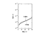
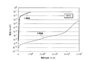
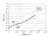
- FIG. 2 is a graph showing IV characteristics of a Cu electrode and an Al electrode, and shows characteristics of an insulating film using a material having a high copper diffusion barrier property. That is, in this example, the IV characteristics of the Cu electrode and the Al electrode are almost the same.
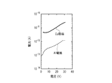
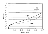
- FIG. 3 is a graph showing characteristics of an insulating film using a material having a low copper diffusion barrier property.
- the IV characteristic due to the Cu electrode is significantly different from the IV characteristic due to the Al electrode, and the current value in the IV characteristic due to the Cu electrode is two digits or more. It is larger than the current value in the characteristics.
- the IV characteristics were measured with the CV measuring apparatus in a state where the sample to be measured on which the Cu electrode was formed was placed in a vacuum probe apparatus and the inside of the apparatus was in a vacuum atmosphere of 0.133 Pa or less. Then, while filling the vacuum probe device with nitrogen until the pressure reached about 93 kPa and heating the stage temperature to 140 ° C. or 200 ° C., the IV characteristics were measured with the CV measuring device.
- the stage temperature used is indicated in the figure.
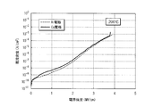
- membrane with high Cu barrier property it evaluated by the one with a higher stage temperature (200 degreeC). By increasing the stage temperature, it is possible to evaluate Cu diffusion more rapidly.
- the measurement of the IV characteristics in the sample to be measured with the Cu electrode formed above was performed in the same manner with the sample to be measured with the Al electrode formed. Due to the difference in the IV characteristics between the Cu electrode and the Al electrode, The copper diffusion barrier property of the formed insulating film was evaluated.
- the evaluation results of the IV characteristics of the insulating film obtained in Example 1 are shown in FIG.
- a spectroscopic ellipsometry apparatus manufactured by Fibravo was used to measure the film thickness used for measuring the relative dielectric constant. Table 1 shows the measurement results of the copper diffusion barrier properties.
- Example 2 Formation of insulating film without using carrier gas-
- the apparatus and method used to form the insulating film are substantially the same as those in Example 1, except that 5-silaspiro [4,4] nonane is circulated as a material gas at a volume flow rate of 35 cc / min to generate a high-frequency power source for generating plasma.
- the output of the apparatus was set to 150 W and an insulating film was formed. At this time, the pressure in the plasma CVD apparatus chamber was 66.6 Pa.
- the relative dielectric constant, copper diffusion barrier property, and film thickness of the obtained insulating film were evaluated in the same manner as in Example 1. The measurement results are shown in Table 1. The evaluation result of the copper diffusion barrier property is shown in FIG.
- Example 3 Formation of Insulating Film Using Carrier Gas
- the apparatus and method used for forming the insulating film are almost the same as those in Example 1, except that 5-silaspiro [4,4] nonane is used as a material gas at a volume flow rate of 17 cc / min, and helium is used as a carrier gas at 40 cc / min.
- the insulating film was formed by setting the output of the high frequency power supply for plasma generation to 150 W. At this time, the pressure in the plasma CVD apparatus chamber was 266 Pa.
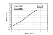
- the dielectric constant, copper diffusion barrier property, and film thickness of the obtained insulating film were evaluated in the same manner as in Example 1. The measurement results are shown in Table 1. The evaluation results of the copper diffusion barrier properties are shown in FIG.
- Example 1 Formation of Insulating Film with Material Gas Containing CH 2 and Containing No Ring Structure
- the apparatus and method used for forming the insulating film are almost the same as those in Example 1, except that tetravinylsilane is used as a material gas at a volume flow of 30 cc / min and helium is used as a carrier gas at a volume flow of 30 cc / min.
- the insulating film was formed by setting the output of the high frequency power supply device for plasma generation to 100 W.
- the plasma CVD apparatus chamber internal pressure at this time was 798 Pa.
- the relative dielectric constant, copper diffusion barrier property, and film thickness of the obtained insulating film were evaluated in the same manner as in Example 1. The measurement results are shown in Table 1. The evaluation result of the copper diffusion barrier property is shown in FIG.
- Example 2 (Comparative Example 2) -Insulation film formation using a material gas containing no cyclic structure composed of CH 2
- the apparatus and method used to form the insulating film are almost the same as in Example 1, but diallyldivinylsilane as a material gas is accompanied by a volume flow of 30 cc / min and helium as a carrier gas at a volume flow of 30 cc / min.
- the insulating film was formed by setting the output of the high frequency power supply for generating plasma to 100 W. At this time, the pressure in the plasma CVD apparatus chamber was 133 Pa.
- the relative dielectric constant, copper diffusion barrier property, and film thickness of the obtained insulating film were evaluated in the same manner as in Example 1. The measurement results are shown in Table 1. The evaluation results of the copper diffusion barrier properties are shown in FIG.
- Example 3 Comparative Example 3 (Reference Example)-Formation of Insulating Film by Material Gas Containing Ring Structure Partly of CH 2-
- the apparatus and method used to form the insulating film are almost the same as those in Example 1, but 1,1-divinyl-1-containing a single cyclic structure bonded to silicon and made of CH 2 as a material gas.
- Silacyclopentane was circulated as a carrier gas at a volume flow rate of 17 cc / min and helium was allowed to flow at a volume flow rate of 40 cc / min, and the output of the high frequency power supply for plasma generation was set to 150 W to form an insulating film.
- the pressure in the plasma CVD apparatus chamber was 133 Pa.
- 1,1-divinyl-1-silacyclopentane has been found to have an excellent effect as an insulating film material by the inventors of the present application (see JP 2009-176898 A). If there is an effect similar to or higher than this, it can be determined that the desired effect has been achieved.
- the relative dielectric constant, copper diffusion barrier property, and film thickness of the obtained insulating film were evaluated in the same manner as in Example 1. The measurement results are shown in Table 1. The evaluation results of the copper diffusion barrier properties are shown in FIG.
- the insulating film formed in Example 1 has a relative dielectric constant of 3.22 and a copper diffusion barrier property.
- the formed insulating film has a relative dielectric constant of 3.55 and has a copper diffusion barrier property
- the insulating film formed in Example 3 has a relative dielectric constant of 3.39 and has a copper diffusion barrier property.
- Example 3 since the carrier gas was used, a slight difference in IV characteristics was seen compared to the other examples, but this is in a range where there is no problem in use.
- the insulating film formed in Comparative Example 1 has a relative dielectric constant of 2.87 and does not have a copper diffusion barrier property
- the insulating film formed in Comparative Example 2 has a relative dielectric constant of 2.72. It did not have a copper diffusion barrier property.
- Comparative Examples 1 and 2 an insulating film having a low dielectric constant but no copper diffusion barrier property was obtained.
- the insulating film formed in Comparative Example 3 (Reference Example) had a relative dielectric constant of 3.38 and had a copper diffusive barrier property. It can be judged that Examples 1 to 3 have the same or higher effect as Comparative Example 3 (Reference Example). Therefore, Examples 1 to 3 are known in the art that have both a Cu barrier property and a low relative dielectric constant. It was confirmed that the material has the same performance as that of the excellent material.
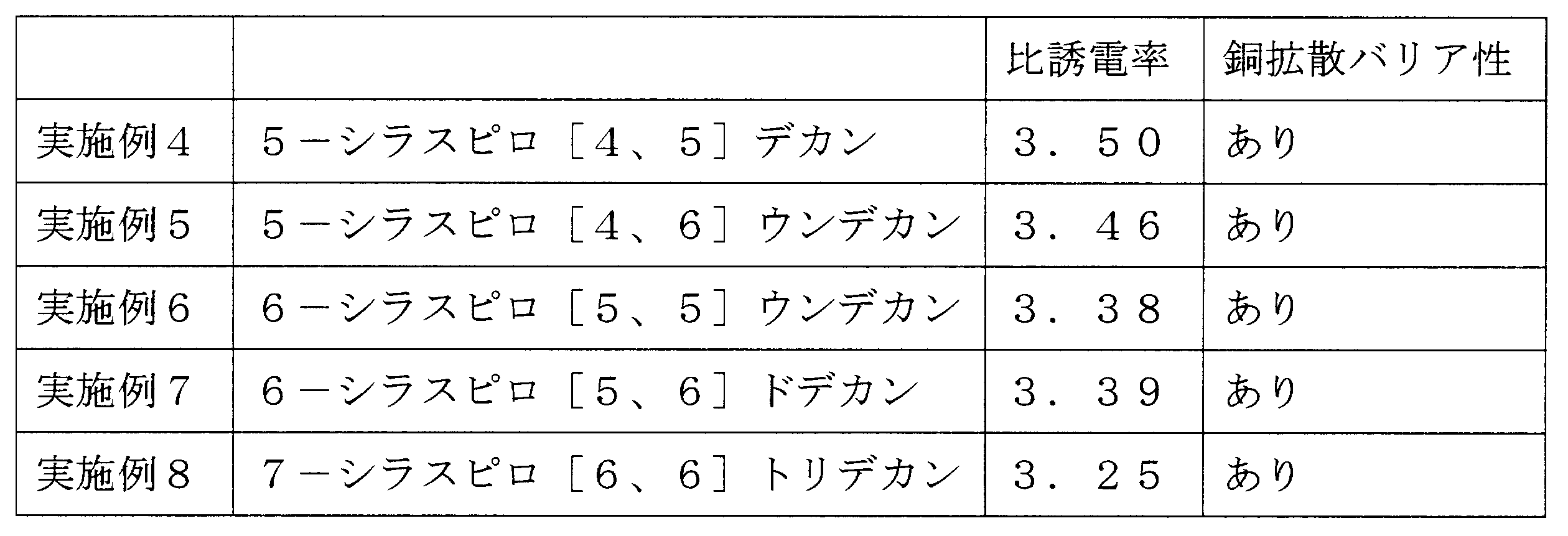
- Examples 4-8 In Examples 1 to 3, evaluation was made using 5-silaspiro [4,4] nonane, but it goes without saying that other compounds within the scope of the present application also have excellent effects. The experiment was conducted in the same manner as in Example 1 except that the following compound was used instead of 5-silaspiro [4,4] nonane. From any compound, an insulating film having a copper diffusion barrier property and a low relative dielectric constant was obtained.
- an insulating film is formed by a plasma CVD method using an insulating film material made of a silicon compound represented by the chemical formula (1), so that an insulation having a copper diffusion barrier property and a low relative dielectric constant is obtained.
- a film can be formed.
- an insulating film having a lower dielectric constant suitable for the next generation application can be formed.
- Such an insulating film can be preferably used as a copper diffusion barrier insulating film.
- the insulating film of the present invention can be preferably used as an interlayer insulating film. If the insulating film of the present invention is used as an interlayer insulating film, a copper diffusion barrier insulating film can be further omitted as required.
- the present invention can be applied to a semiconductor device using highly integrated LSI wiring required for the next generation.
Landscapes
- Chemical & Material Sciences (AREA)
- Inorganic Chemistry (AREA)
- General Chemical & Material Sciences (AREA)
- Chemical Kinetics & Catalysis (AREA)
- Engineering & Computer Science (AREA)
- Materials Engineering (AREA)
- Mechanical Engineering (AREA)
- Metallurgy (AREA)
- Organic Chemistry (AREA)
- Internal Circuitry In Semiconductor Integrated Circuit Devices (AREA)
- Chemical Vapour Deposition (AREA)
- Formation Of Insulating Films (AREA)
Abstract
Description
本願は、2008年9月1日に、日本に出願された特願2008-223907号に基づき優先権を主張し、その内容をここに援用する。
例えば、層間絶縁膜としては、SiO2膜が4.1、SiOF膜が3.7の比誘電率を有するが、近年では、さらに比誘電率の低いSiOCH膜や有機膜を用いるようになっている。
この銅拡散バリア性絶縁膜には、優れた銅拡散バリア性を有する窒化ケイ素やSiCNなどからなる絶縁膜が用いられている。しかしながらこれら膜の比誘電率は4~7と高い。このような高い比誘電率は多層配線構造を構成する絶縁膜全体としての実効的な比誘電率を高くしている。
例えば、比誘電率が2.5程度の層間絶縁膜を用いたとしても、比誘電率が2.5程度の層間絶縁膜と、比誘電率が4程度の銅拡散バリア性絶縁膜とを積層させた多層配線構造では、この構造の実効的な比誘電率は3程度となる。
例えば、これまでに、π電子結合を持つ有機シラン系材料を用いた、ケイ素と炭素を主成分とする銅拡散バリア性絶縁膜についての報告がある(特許文献1参照)。
このように、低比誘電率と銅拡散バリア性をバランスよく有する絶縁膜であって、さらに好ましくは銅を酸化させる酸素を含まない材料からなる絶縁膜が求められていたが、そのような絶縁膜はこれまであまり報告されていなかった。
(i)本発明の第一の態様は、下記化学式(1)で示されるプラズマCVD用絶縁膜材料である。

(iii)本発明のプラズマCVD用絶縁膜材料は、分子中に、炭素の二重結合を含まないことを特徴とする。
(iv)本発明のプラズマCVD用絶縁膜材料は、分子中に、ケイ素に結合し、かつCH2からなる環状構造を2つ含むことを特徴とする。
(vi)第二の態様の成膜方法は、成膜の際、キャリアガスを同伴させない事が好ましい。
(viii)本発明の第三の態様の絶縁膜は、比誘電率が3.5以下である事が好ましい。
(iv)本発明の第四の態様は、本発明の第一の態様の絶縁膜材料の、プラズマCVD法を用いた絶縁膜の形成への使用である。
本発明の絶縁膜は、配線層及び層間絶縁膜を含む多層配線構造における、層間絶縁膜である事が好ましい。
本発明の絶縁膜は、配線層、銅拡散バリア性絶縁膜、及び層間絶縁膜とを含む多層配線構造における、銅拡散バリア性絶縁膜である事が好ましい。
本発明の絶縁膜の比誘電率は、好ましくは2.9~3.5である。
以下、本発明を詳しく説明する。
本発明のプラズマCVD用絶縁膜材料は、前記化学式(1)で表されるケイ素化合物であり、この範囲のすべて公知化合物であって良く、また公知合成方法により得ることができる。なおこの化学式(1)で示される化合物を、銅拡散バリア性絶縁膜材料として使用することは、従来知られていない。前記課題を解決すべく行われた本発明者の鋭意検討によって、新たに見出されたものである。
このケイ素化合物は、分子内に3員環から6員環から選択される環状構造を2つ有し、いずれの環においても(CH2)mや(CH2)nの両端部の炭素が、ケイ素原子に直接結合している。またこの環状構造内には、二重結合が含まれていない。
これ以外に用いられるケイ素化合物の例としては、4-シラスピロ[3、3]ヘプタン、4-シラスピロ[3、4]オクタン、4-シラスピロ[3、5]ノナン、4-シラスピロ[3、6]デカン、5-シラスピロ[4、5]デカン、5-シラスピロ[4、6]ウンデカン、6-シラスピロ[5、5]ウンデカン、6-シラスピロ[5、6]ドデカン、7-シラスピロ[6、6]トリデカンなどがあげられる。
本発明の成膜方法は、基本的には、上述の化学式(1)に示される絶縁膜材料を用いプラズマCVD法により成膜を行う。この場合、化学式(1)で示されるケイ素化合物を1種使用してもよく、または2種以上を混合して使用することもできる。
また、成膜の際に、前記化学式(1)で示されるケイ素化合物からなる絶縁膜材料にキャリアガスを添加して成膜することもできる。ただし銅拡散バリア性の改善のためには、本発明の絶縁膜材料を単独で成膜する方が好ましい。
したがって、成膜装置のチャンバー内に送り込まれ成膜に供される成膜用ガスは、絶縁膜材料のみからなるガスの他に、キャリアガスが混合された混合ガスとなることがある。
図1に示したプラズマ成膜装置は、減圧可能なチャンバー1を備え、このチャンバー1は、排気管2、及び開閉弁3を介して排気ポンプ4に接続されている。また、チャンバー1には、図示しない圧力計が備えられ、チャンバー1内の圧力が測定できる。チャンバー1内には、相対向する一対の平板状の上部電極5と下部電極6とが設けられている。上部電極5は、高周波電源7に接続されており、上部電極5に高周波電流が印加されるようになっている。
また、上部電極5には、ガス供給配管10が接続されている。このガス供給配管10には、図示しない成膜用ガス供給源が接続され、この成膜用ガス供給装置からの成膜用のガスが供給され、このガスは上部電極5内に形成された複数の貫通孔を通って、下部電極6に向けて拡散しつつ流れ出る構成になっている。
基板8には、主にシリコンウェーハからなるものが用いられる。このシリコンウェーハ上には、あらかじめ形成された他の絶縁膜、導電膜、及び/又は配線構造などが存在していてもよい。
絶縁膜材料流量 :15~100cc/分 (2種以上の場合は合計量である)
キャリアガス流量 :0~80cc/分
圧力 :1Pa~1330Pa
RFパワー :50~500W、好ましくは50~250W
基板温度 :400℃以下
反応時間 :1秒~180秒
成膜厚さ :100nm~200nm
本発明の絶縁膜は、上述のプラズマCVD用絶縁膜材料、またはこれとキャリアガスとを用い、プラズマ成膜装置によって、プラズマCVD反応により成膜される。その比誘電率は一般的には3.5以下であり、より好ましくは2.9~3.5であり、これは更に銅拡散バリア性が高い。また、この絶縁膜は、酸素が含まれておらず、ケイ素と水素と炭素から構成されている。
すなわち、本発明の絶縁膜材料をなすケイ素化合物において、ケイ素に結合する環状構造では、C-C部分の結合エネルギーが最も低く、その為、プラズマによりこの結合は切断され開環される。
以上より、本発明の絶縁膜が、低比誘電率を有しかつ銅拡散バリア性を有する絶縁膜となるものと考えられる。
以下のように絶縁膜を形成した。
平行平板型の容量結合プラズマCVD装置を使用し、あらかじめ350℃程度に加熱したサセプター上に、8インチ(直径200mm)のシリコンウェーハを搬送し、絶縁膜材料ガスとして5-シラスピロ[4,4]ノナンを20cc/minの体積流量で流通させ、プラズマ発生用高周波電源装置の出力を180Wに設定して絶縁膜を形成した。このときの前記プラズマCVD装置のチャンバー内圧力は133Paであった。
得られた絶縁膜の比誘電率を測定するために、前記シリコンウェーハをSSM社製CV測定装置495上に搬送し、水銀電極を用いて絶縁膜の比誘電率を測定した。測定結果を表1に示す。
得られた絶縁膜の銅拡散バリア性の評価には、得られた絶縁膜に、銅電極(以下、Cu電極)とアルミニウム電極(以下、Al電極)をそれぞれ用いた場合における電流-電圧(I-V)特性を表にし、それらの相違を比較する方法を採用した。
これは、絶縁膜を100℃~300℃程度に加熱した状態で電界をかけることにより、銅の絶縁膜中への拡散が加速されることを利用したBiased Temperature Stress試験法である。
図3は、銅拡散バリア性が低い材料を用いた絶縁膜の特性を示したグラフである。この例では、Cu電極によるI-V特性とAl電極とによるI-V特性とが大きく異なっており、Cu電極よるI-V特性での電流値が2桁以上、Al電極とによるI-V特性での電流値よりも大きくなっている。
この試験方法に関しては、以下の文献を参照することができる。
まず、30mm2程度に切り出した被測定サンプルを2つ作成し、マスクをかけ、一方に直径約1mmのCu電極を、他方に直径約1mmのAl電極を真空蒸着により形成する。
その他、比誘電率の測定に使用する膜厚の測定には、ファイブラボ社製分光エリプソメトリ装置を使用した。
銅拡散バリア性の測定結果を表1に示す。
絶縁膜を形成するにあたって使用する装置および方法は実施例1とほぼ同じであるが、材料ガスとして5-シラスピロ[4,4]ノナンを35cc/minの体積流量で流通させ、プラズマ発生用高周波電源装置の出力を150Wに設定して絶縁膜を形成した。このときの前記プラズマCVD装置チャンバー内圧力は66.6Paであった。
絶縁膜を形成するにあたって使用する装置および方法は実施例1とほぼ同じであるが、材料ガスとして5-シラスピロ[4,4]ノナンを17cc/minの体積流量で、キャリアガスとしてヘリウムを40cc/minで同伴して流通させ、プラズマ発生用高周波電源装置の出力を150Wに設定して絶縁膜を形成した。このときの前記プラズマCVD装置チャンバー内圧力は266Paであった。
測定結果を表1に示す。銅拡散バリア性の評価結果を図6に示す。
絶縁膜を形成するにあたって使用する装置および方法は実施例1とほぼ同じであるが、材料ガスとしてテトラビニルシランを30cc/minの体積流量でキャリアガスとしてヘリウムを30cc/minの体積流量で同伴して流通させ、プラズマ発生用高周波電源装置の出力を100Wに設定して絶縁膜を形成した。このときの前記プラズマCVD装置チャンバー内圧力は798Paであった。
絶縁膜を形成するにあたって使用する装置および方法は実施例1とほぼ同じであるが、材料ガスとしてジアリルジビニルシランを30cc/minの体積流量でキャリアガスとしてヘリウムを30cc/minの体積流量で同伴して流通させ、プラズマ発生用高周波電源装置の出力を100Wに設定して絶縁膜を形成した。このときの前記プラズマCVD装置チャンバー内圧力は133Paであった。
絶縁膜を形成するにあたって使用する装置および方法は実施例1とほぼ同じであるが、材料ガスとして、ケイ素に結合しかつCH2からなる環状構造を1つ含む、1,1-ジビニル-1-シラシクロペンタンを17cc/minの体積流量でキャリアガスとしてヘリウムを40cc/minの体積流量で同伴して流通させ、プラズマ発生用高周波電源装置の出力を150Wに設定して絶縁膜を形成した。このときの前記プラズマCVD装置チャンバー内圧力は133Paであった。
なお1,1-ジビニル-1-シラシクロペンタンは、本願発明者らによって既に絶縁膜材料としての優れた効果が見出されていたものである(特開2009-176898参照)。これと同程度、あるいはそれ以上の効果を有すれば、目的の効果が達成されたと判断できる。
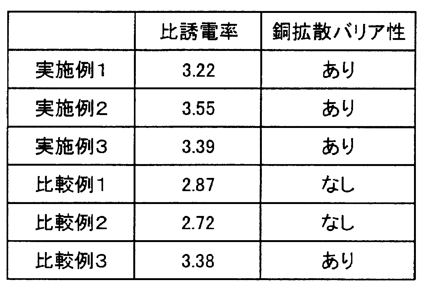
一方で、比較例1で形成された絶縁膜は比誘電率が2.87であり銅拡散バリア性を有せず、比較例2で形成された絶縁膜は比誘電率が2.72であり銅拡散バリア性を有しなかった。このように比較例1~2では、比誘電率が低いものの、銅拡散バリア性を有しない絶縁膜が得られた。比較例3(参考例)で形成された絶縁膜は、比誘電率が3.38であり銅拡散性バリア性質を有していた。実施例1~3は、比較例3(参考例)と同程度あるいはそれ以上の効果が得られたと判断でき、よって、実施例1~3は、Cuバリア性と低い比誘電率を両立する公知の優れた材料と同等な性能を有することが確認された。
実施例1~3では、5-シラスピロ[4,4]ノナンを用いて評価したが、それ以外の本願範囲に含まれる化合物も優れた効果を有する事はもちろんである。5-シラスピロ[4,4]ノナンの代わりに、以下の化合物を用いた以外は実施例1と同様に実験を行った。どの化合物からも、銅拡散バリア性を有しつつ、比誘電率が高くない絶縁膜が得られた。
2 排気管
3 開閉弁
4 排気ポンプ
5 上部電極
6 下部電極
7 高周波電源
8 基板
9 ヒータ
10 ガス供給配管
Claims (12)
- 下記化学式(1)で示されるプラズマCVD用絶縁膜材料。

- 分子中に、酸素を含まないことを特徴とする請求項1に記載のCVD用絶縁膜材料。
- 分子中に、炭素の二重結合を含まないことを特徴とする請求項1に記載のCVD用絶縁膜材料。
- 分子中に、ケイ素に結合し、かつCH2からなる環状構造を2つ含むことを特徴とする請求項1に記載のCVD用絶縁膜材料。
- 請求項1に記載の絶縁膜材料を用い、プラズマCVD法により、絶縁膜を成膜する成膜方法。
- 成膜の際、キャリアガスを同伴させない請求項5に記載の成膜方法。
- 請求項5に記載の成膜方法で得られた絶縁膜。
- 絶縁膜の比誘電率が3.5以下である請求項7に記載の絶縁膜。
- 請求項1に記載の絶縁膜材料の、プラズマCVD法を用いた絶縁膜の形成への使用。
- プラズマCVD法を用いた、配線層及び層間絶縁膜を含む多層配線構造における層間絶縁膜の形成への、請求項9に記載の絶縁膜材料の使用。
- プラズマCVD法を用いた、配線層、銅拡散バリア性絶縁膜、及び層間絶縁膜、とを含む多層配線構造における銅拡散バリア性絶縁膜の形成への、請求項9に記載の絶縁膜材料の使用。
- 絶縁膜の比誘電率が2.9~3.5である請求項7に記載の絶縁膜。
Priority Applications (2)
| Application Number | Priority Date | Filing Date | Title |
|---|---|---|---|
| US13/060,525 US20110159212A1 (en) | 2008-09-01 | 2009-09-01 | Insulating film material, method for forming film by using the insulating film material, and insulating film |
| CN2009801340046A CN102138205A (zh) | 2008-09-01 | 2009-09-01 | 绝缘膜材料、使用该绝缘膜材料的成膜方法和绝缘膜 |
Applications Claiming Priority (2)
| Application Number | Priority Date | Filing Date | Title |
|---|---|---|---|
| JP2008223907A JP5505680B2 (ja) | 2008-09-01 | 2008-09-01 | 絶縁膜材料、この絶縁膜材料を用いた成膜方法および絶縁膜 |
| JP2008-223907 | 2008-09-01 |
Publications (1)
| Publication Number | Publication Date |
|---|---|
| WO2010023964A1 true WO2010023964A1 (ja) | 2010-03-04 |
Family
ID=41721145
Family Applications (1)
| Application Number | Title | Priority Date | Filing Date |
|---|---|---|---|
| PCT/JP2009/004298 Ceased WO2010023964A1 (ja) | 2008-09-01 | 2009-09-01 | 絶縁膜材料、この絶縁膜材料を用いた成膜方法および絶縁膜 |
Country Status (6)
| Country | Link |
|---|---|
| US (1) | US20110159212A1 (ja) |
| JP (1) | JP5505680B2 (ja) |
| KR (1) | KR101635120B1 (ja) |
| CN (1) | CN102138205A (ja) |
| TW (1) | TW201016710A (ja) |
| WO (1) | WO2010023964A1 (ja) |
Cited By (1)
| Publication number | Priority date | Publication date | Assignee | Title |
|---|---|---|---|---|
| WO2010090038A1 (ja) * | 2009-02-06 | 2010-08-12 | 独立行政法人物質・材料研究機構 | 絶縁膜材料、この絶縁膜材料を用いた成膜方法および絶縁膜 |
Families Citing this family (2)
| Publication number | Priority date | Publication date | Assignee | Title |
|---|---|---|---|---|
| JP5750230B2 (ja) * | 2010-03-29 | 2015-07-15 | 大陽日酸株式会社 | 炭窒化珪素膜及び炭窒化珪素膜の成膜方法 |
| US9177783B2 (en) | 2013-12-10 | 2015-11-03 | Applied Materials, Inc. | Substituted silacyclopropane precursors and their use for the deposition of silicon-containing films |
Citations (1)
| Publication number | Priority date | Publication date | Assignee | Title |
|---|---|---|---|---|
| JP2006519496A (ja) * | 2003-02-26 | 2006-08-24 | ダウ・コーニング・コーポレイション | 水素化シリコンオキシカーバイド膜の生成方法。 |
Family Cites Families (7)
| Publication number | Priority date | Publication date | Assignee | Title |
|---|---|---|---|---|
| FR2575466B1 (fr) * | 1984-12-27 | 1987-02-20 | Centre Nat Rech Scient | Nouveaux complexes de silicium hexacoordines, leur procede de preparation et leur application |
| US5384289A (en) * | 1993-06-17 | 1995-01-24 | Micron Semiconductor, Inc. | Reductive elimination chemical vapor deposition processes utilizing organometallic precursor compounds in semiconductor wafer processing |
| KR100615410B1 (ko) * | 2000-08-02 | 2006-08-25 | 인터내셔널 비지네스 머신즈 코포레이션 | 저 유전 상수 다상 물질 및 그 증착 방법 |
| US6716770B2 (en) * | 2001-05-23 | 2004-04-06 | Air Products And Chemicals, Inc. | Low dielectric constant material and method of processing by CVD |
| JP2004149607A (ja) * | 2002-10-29 | 2004-05-27 | Jsr Corp | 多層配線間の空洞形成用重合体およびその製造方法 |
| JP2005045058A (ja) | 2003-07-23 | 2005-02-17 | Mitsui Chemicals Inc | 銅拡散バリア性絶縁膜の形成方法およびその絶縁膜 |
| EP1916253A1 (en) * | 2006-10-26 | 2008-04-30 | L'AIR LIQUIDE, Société Anonyme pour l'Etude et l'Exploitation des Procédés Georges Claude | New group V metal containing precursors and their use for metal containing film deposition |
-
2008
- 2008-09-01 JP JP2008223907A patent/JP5505680B2/ja not_active Expired - Fee Related
-
2009
- 2009-09-01 TW TW098129349A patent/TW201016710A/zh unknown
- 2009-09-01 KR KR1020117005949A patent/KR101635120B1/ko not_active Expired - Fee Related
- 2009-09-01 CN CN2009801340046A patent/CN102138205A/zh active Pending
- 2009-09-01 WO PCT/JP2009/004298 patent/WO2010023964A1/ja not_active Ceased
- 2009-09-01 US US13/060,525 patent/US20110159212A1/en not_active Abandoned
Patent Citations (1)
| Publication number | Priority date | Publication date | Assignee | Title |
|---|---|---|---|---|
| JP2006519496A (ja) * | 2003-02-26 | 2006-08-24 | ダウ・コーニング・コーポレイション | 水素化シリコンオキシカーバイド膜の生成方法。 |
Non-Patent Citations (1)
| Title |
|---|
| GERAULT, J. P., THIN SOLID FILMS, vol. 101, no. 1, 1983, pages 83 - 96 * |
Cited By (1)
| Publication number | Priority date | Publication date | Assignee | Title |
|---|---|---|---|---|
| WO2010090038A1 (ja) * | 2009-02-06 | 2010-08-12 | 独立行政法人物質・材料研究機構 | 絶縁膜材料、この絶縁膜材料を用いた成膜方法および絶縁膜 |
Also Published As
| Publication number | Publication date |
|---|---|
| JP5505680B2 (ja) | 2014-05-28 |
| CN102138205A (zh) | 2011-07-27 |
| KR20110055643A (ko) | 2011-05-25 |
| JP2010062218A (ja) | 2010-03-18 |
| TW201016710A (en) | 2010-05-01 |
| US20110159212A1 (en) | 2011-06-30 |
| KR101635120B1 (ko) | 2016-06-30 |
Similar Documents
| Publication | Publication Date | Title |
|---|---|---|
| JP5317089B2 (ja) | 成膜方法および絶縁膜 | |
| JP3930840B2 (ja) | 低κ誘電性無機/有機ハイブリッドフィルム | |
| JP3600507B2 (ja) | 半導体装置及びその製造方法 | |
| KR100407012B1 (ko) | 반도체 장치 및 그 제조 방법 | |
| US9111761B2 (en) | Multi component dielectric layer | |
| US20120301706A1 (en) | METHOD OF PE-ALD OF SiNxCy AND INTEGRATION OF LINER MATERIALS ON POROUS LOW K SUBSTRATES | |
| TWI490363B (zh) | 絕緣膜材料、使用該絕緣膜材料的成膜方法及絕緣膜 | |
| JP5320570B2 (ja) | 層間絶縁膜、配線構造および電子装置と、それらの製造方法 | |
| JP3934343B2 (ja) | 半導体装置及びその製造方法 | |
| JP5505680B2 (ja) | 絶縁膜材料、この絶縁膜材料を用いた成膜方法および絶縁膜 | |
| KR20230055964A (ko) | 펄스형 화학 기상 증착을 사용하여 질화붕소를 증착하기 위한 방법 및 시스템 | |
| JP2007318067A (ja) | 絶縁膜材料、この絶縁膜材料を用いた成膜方法および絶縁膜 | |
| JP5731841B2 (ja) | シリコン窒化膜の形成方法 | |
| JP5750230B2 (ja) | 炭窒化珪素膜及び炭窒化珪素膜の成膜方法 | |
| WO2011108456A1 (ja) | 低誘電率層間絶縁膜および低誘電率層間絶縁膜の成膜方法 | |
| JP5607394B2 (ja) | 層間絶縁膜の成膜方法および層間絶縁膜 | |
| JP2002329718A (ja) | 半導体基板上のシロキサン重合体膜及びその製造方法 | |
| KR20030007724A (ko) | 집적 회로 구조 | |
| WO2006109686A1 (ja) | 絶縁膜用材料およびその成膜方法 | |
| JP2007318070A (ja) | 絶縁膜材料、この絶縁膜材料を用いた成膜方法および絶縁膜 | |
| JP2006294671A (ja) | 低誘電率炭化珪素膜の製造方法 | |
| JP2009277686A (ja) | 絶縁膜の成膜方法および絶縁膜 |
Legal Events
| Date | Code | Title | Description |
|---|---|---|---|
| WWE | Wipo information: entry into national phase |
Ref document number: 200980134004.6 Country of ref document: CN |
|
| 121 | Ep: the epo has been informed by wipo that ep was designated in this application |
Ref document number: 09809619 Country of ref document: EP Kind code of ref document: A1 |
|
| NENP | Non-entry into the national phase |
Ref country code: DE |
|
| ENP | Entry into the national phase |
Ref document number: 20117005949 Country of ref document: KR Kind code of ref document: A |
|
| 122 | Ep: pct application non-entry in european phase |
Ref document number: 09809619 Country of ref document: EP Kind code of ref document: A1 |