WO2010023924A1 - 相互接続基板、スキュー測定方法および試験装置 - Google Patents
相互接続基板、スキュー測定方法および試験装置 Download PDFInfo
- Publication number
- WO2010023924A1 WO2010023924A1 PCT/JP2009/004177 JP2009004177W WO2010023924A1 WO 2010023924 A1 WO2010023924 A1 WO 2010023924A1 JP 2009004177 W JP2009004177 W JP 2009004177W WO 2010023924 A1 WO2010023924 A1 WO 2010023924A1
- Authority
- WO
- WIPO (PCT)
- Prior art keywords
- signal
- output
- skew
- test
- output pin
- Prior art date
- Legal status (The legal status is an assumption and is not a legal conclusion. Google has not performed a legal analysis and makes no representation as to the accuracy of the status listed.)
- Ceased
Links
Images




Classifications
-
- G—PHYSICS
- G01—MEASURING; TESTING
- G01R—MEASURING ELECTRIC VARIABLES; MEASURING MAGNETIC VARIABLES
- G01R31/00—Arrangements for testing electric properties; Arrangements for locating electric faults; Arrangements for electrical testing characterised by what is being tested not provided for elsewhere
- G01R31/28—Testing of electronic circuits, e.g. by signal tracer
- G01R31/317—Testing of digital circuits
- G01R31/31725—Timing aspects, e.g. clock distribution, skew, propagation delay
-
- G—PHYSICS
- G01—MEASURING; TESTING
- G01R—MEASURING ELECTRIC VARIABLES; MEASURING MAGNETIC VARIABLES
- G01R31/00—Arrangements for testing electric properties; Arrangements for locating electric faults; Arrangements for electrical testing characterised by what is being tested not provided for elsewhere
- G01R31/28—Testing of electronic circuits, e.g. by signal tracer
-
- G—PHYSICS
- G01—MEASURING; TESTING
- G01R—MEASURING ELECTRIC VARIABLES; MEASURING MAGNETIC VARIABLES
- G01R35/00—Testing or calibrating of apparatus covered by the other groups of this subclass
Definitions
- the present invention relates to a wiring board, a skew measurement method, and a test apparatus.
- This application is related to the following US applications and claims priority from the following US applications: For designated countries where incorporation by reference of documents is permitted, the contents described in the following application are incorporated into this application by reference and made a part of this application.
- a test apparatus for testing a device under test such as a semiconductor device or an electronic device supplies a test signal to the device under test and compares the output signal of the device under test with a predetermined expected value signal. Test the test device. The test apparatus adjusts the phase, frequency, etc. of the test signal and then supplies the test signal to the device under test.
- Patent Document 1 describes a test apparatus that tests a device under test that outputs a differential signal by supplying a differential signal to a differential terminal of the device under test via a differential driver. (See Patent Document 1). The test apparatus of Patent Document 1 adjusts the skew of the differential signal so that the differential signal correctly crosses at the differential terminal of the device under test. JP-A-2005-293808
- an object of one aspect of the present invention is to provide a wiring board, a skew measurement method, and a test apparatus that can solve the above-described problems. This object is achieved by a combination of features described in the independent claims.
- the dependent claims define further advantageous specific examples of the present invention.
- the wiring used for measuring the skew between the output pins in the test apparatus for testing the device under test by supplying the device under test with the test signal including the first signal and the second signal.
- a wiring board comprising a second wiring connecting between the two terminals and the binding node and a third wiring connecting between the binding node and the output node, wherein the first wiring and the second wiring are formed to have equal lengths.
- the wiring board may be formed such that the first wiring and the second wiring are equal and have the shortest length.
- the test apparatus includes a timing measurement circuit and an input terminal connected to the timing measurement circuit, and an output node of the wiring board is a third terminal coupled to the input terminal of the test apparatus. It may be.
- the wiring board may further include a timing measurement circuit, and the output node may be an input node of the timing measurement circuit.
- the first signal output from the first output pin of the test apparatus is a normal phase signal of the test signal
- the second signal output from the second output pin of the test apparatus is the reverse of the test signal. It may be a phase signal.
- a skew measurement method for measuring a skew between output pins in a test apparatus for testing a device under test by supplying a test signal including a first signal and a second signal to the device under test.
- a step of preparing the wiring board and a second output of the test apparatus for outputting the second signal by coupling the first output pin of the test apparatus for outputting the first signal to the first terminal of the wiring board.
- a skew measurement method is provided.
- the step of measuring skew includes outputting a first signal from the first output pin while maintaining the second output pin at a high level or a low level, and the voltage of the output node is the second output.
- a second signal is output from the second output pin, and a second timing at which the voltage of the output node coincides with a second reference voltage determined based on the relationship between the level of the first output pin and the transition state of the second signal.
- the first output pin outputs a normal phase signal of the test signal
- the second output pin outputs a negative phase signal of the test signal
- the step of measuring the skew occurs at the output node.
- the skew may be measured based on the spike voltage value.
- the first signal and the second signal are a normal phase signal and a negative phase signal of the same test signal, respectively
- the step of measuring the skew includes the step of outputting the same test signal and the output
- the skew may be measured based on the value of the spike voltage generated at the node.
- a test apparatus for testing a device under test by supplying a test signal including a first signal and a second signal to the device under test, the first output pin outputting the first signal;
- a test apparatus including a second output pin that outputs a second signal, a timing measurement circuit that measures the timing of an input signal, and the wiring board.
- FIG. 1 schematically illustrates an exemplary configuration of a test apparatus 100 including a wiring board 104 according to one embodiment.
- An example of a skew measurement method for measuring a skew between output pins in the test apparatus 100 is schematically shown.
- An example of the method of measuring the skew in the test apparatus 100 described with reference to FIG. 2 is schematically shown.
- An example of the measurement process of the 1st timing demonstrated in relation to FIG. 3 is shown roughly.
- An example of the measurement process of a 2nd timing demonstrated in relation to FIG. 3 is shown roughly.
- Another example of measuring the skew of the test apparatus 100 is schematically shown.
- produces in the 3rd terminal 118 demonstrated in relation to FIG. 6 is shown roughly.
- An example of composition of test equipment 800 provided with wiring board 804 concerning another embodiment is shown roughly.
- FIG. 1 schematically shows a configuration example of a test apparatus 100 including a wiring board 104 according to one embodiment.
- the test apparatus 100 includes an apparatus main body 102 and a wiring board 104.
- the apparatus main body 102 gives a test signal to the device under test to test the device under test.
- the wiring board 104 is used for skew measurement or skew adjustment between output pins in the test apparatus 100.
- the test apparatus 100 combines the apparatus main body 102 and the device under test to test the device under test. Moreover, the test apparatus 100 couples the apparatus main body 102 and the wiring board 104 to adjust the skew between the output pins.
- FIG. 1 shows a state in which the apparatus main body 102 and the wiring board 104 are coupled, and therefore, the device under test is not displayed.
- the apparatus main body 102 includes a reference clock generation unit 130 and a test execution unit 132.
- the test execution unit 132 includes a timing generation unit 134, a pattern generation unit 136, a waveform shaping unit 138, a skew adjustment unit 140, a differential driver 150, a first output pin 172, and a second output pin 174.
- the skew adjustment unit 140 includes a variable delay circuit 142 and a variable delay circuit 144.
- the differential driver 150 includes an output resistor 152 and an output resistor 154.
- the test execution unit 132 includes a comparator 162, a pattern comparison unit 164, a termination resistor 166, and an input terminal 176.
- the first output pin 172 and the second output pin 174 may be examples of output pins.
- the comparator 162 may be an example of a timing measurement circuit that measures transition timing of an input signal.
- the apparatus main body 102 may include a plurality of test execution units 132. Thereby, even if the device under test has a plurality of blocks under test, the test apparatus 100 can test a plurality of blocks under test simultaneously.
- the wiring board 104 includes a first terminal 112 coupled to the first output pin 172, a second terminal 114 coupled to the second output pin 174, a binding node 116, and a third terminal coupled to the input terminal 176. 118.
- the third terminal 118 may be an example of an output node.
- the wiring board 104 includes a first wiring 122 that connects the first terminal 112 and the binding node 116, a second wiring 124 that connects the second terminal 114 and the binding node 116, and the binding node 116 and the third terminal. And a third wiring 126 connecting between the first wiring 118 and the second wiring 126.
- the test operation of the device under test by the test apparatus 100 will be described.
- the test signal output from the first output pin 172 of the test apparatus 100 may be a normal phase signal
- the test signal output from the second output pin 174 of the test apparatus 100 is a reverse phase signal. It's okay.
- the positive phase signal may be an example of a first signal.
- the negative phase signal may be an example of a second signal.
- the reference clock generator 130 generates a reference clock for the test apparatus 100.
- the reference clock generation unit 130 supplies the reference clock to the timing generation unit 134 and the pattern generation unit 136.
- the timing generation unit 134 generates a timing signal and supplies it to the waveform shaping unit 138.
- the timing signal defines the timing at which the test signal supplied to the device under test is generated as a voltage signal.
- the pattern generation unit 136 generates a pattern signal and supplies it to the waveform shaping unit 138.
- the pattern signal defines the test pattern of the test signal.
- the pattern signal may be a digital pattern signal.
- the pattern generation unit 136 generates an expected value signal corresponding to the test signal and supplies it to the pattern comparison unit 164.
- the waveform shaping unit 138 shapes the pattern signal supplied from the pattern generation unit 136 and the timing signal supplied from the timing generation unit into a waveform suitable for the test of the device under test.
- the waveform shaping unit 138 supplies the shaped waveform to the device under test via the skew adjustment unit 140 and the differential driver 150.
- the waveform shaping unit 138 generates a strobe signal and supplies it to the comparator 162.
- the strobe signal is used to determine the timing phase of the signal input from the input terminal 176.
- the skew adjustment unit 140 adjusts the skew between the normal phase signal component and the negative phase signal component of the test signal supplied from the waveform shaping unit 138.
- the variable delay circuit 142 adjusts the phase of the positive phase signal component.
- the variable delay circuit 144 adjusts the phase of the anti-phase signal component.
- the skew adjustment unit 140 supplies the positive-phase signal component and the negative-phase signal component whose skew has been adjusted to the differential driver 150.
- the differential driver 150 supplies the positive phase signal component of the test signal supplied from the skew adjustment unit 140 to the first output pin 172 that outputs the test signal via the output resistor 152.
- the differential driver 150 supplies the reverse phase signal component of the test signal supplied from the skew adjustment unit 140 to the second output pin 174 that outputs the test signal via the output resistor 154.
- the resistivity of the output resistor 152 and the output resistor 154 may be the same.
- a termination voltage source may be coupled to the wiring between one input terminal of the comparator 162 and the input terminal 176 via a termination resistor 166.
- the termination voltage source applies a voltage VTT .
- a reference voltage source may be coupled to the other input terminal of the comparator 162.
- the reference voltage source applies a voltage VREF .
- Termination resistor 166 may have the same resistivity as output resistor 152 and output resistor 154. In FIG. 1, drawing of the termination voltage source and the reference voltage source is omitted.
- the comparator 162 compares the voltage of the output signal supplied from the input terminal 176 with V REF and supplies the comparison result to the pattern comparison unit 164. For example, when the voltage of the output signal is lower than V REF , the comparator 162 outputs L logic as the comparison result. On the other hand, when the voltage of the output signal is higher than V REF , the comparator 162 outputs H logic as the comparison result.
- the comparator 162 measures the transition timing of the input signal.
- the comparator 162 may measure the transition timing of the output signal of the device under test based on the strobe signal supplied from the waveform shaping unit 138.
- the pattern comparison unit 164 compares the expected value signal supplied from the pattern generation unit 136 with the comparison result supplied from the comparator 162 to determine pass / fail of the device under test. Although not shown in FIG. 1, the pattern comparison unit 164 may supply the test result to, for example, the apparatus main body 102.
- the skew adjustment between the output pins of the test apparatus 100 will be examined.
- a method of adjusting the skew between the output pins of the test apparatus 100 for example, using a probing robot having a broadband probe connected to the robot arm, directly contacting the output pin to be observed and observing the output signal Can be considered.
- the probing robot is not shown in FIG.
- the calibration of skew between output pins using a probing robot can be executed by the following procedure, for example.
- the test execution unit 132 outputs a differential signal including a normal phase signal and a negative phase signal as an example, the differential signal skew
- the procedure for calibrating is described.
- the broadband probe with one output pin of the pair of output pins you want to calibrate.
- the positive phase signal is measured by contacting the first output pin 172.
- the timing at which the positive phase signal rises is measured with a high-accuracy timing measuring instrument.
- a timing point at which the amplitude is 50% is measured with a high-precision timing measuring instrument.
- the broadband probe moves the broadband probe so that it contacts the other output pin of the pair of output pins that you want to calibrate.
- the negative phase signal is measured by contacting the second output pin 174.
- the timing at which the negative phase signal falls is measured with a high precision timing measuring instrument.
- the differential skew is obtained as a difference between a timing point obtained by measuring the first output pin 172 and a timing point obtained by measuring the second output pin 174.
- the test apparatus 100 adjusts the setting of the skew adjustment unit 140 so that the differential skew is within a predetermined range. This completes the calibration of the differential skew between the pair of output pins.
- the wideband probe is moved to calibrate the differential skew between another pair of output pins.
- the calibration of the test apparatus 100 can be executed by repeating the calibration of the skew between the pair of output pins.
- the skew between output pins can be calibrated by using a probing robot.
- the measurement time is long.
- installation and operation of the probing robot is time consuming and lacks operability.
- the test apparatus 100 outputs a differential signal, since the frequency response characteristics of the first output pin 172 and the second output pin 174 are different, if a differential signal having a frequency different from the frequency at which calibration is performed is output, Skew gets worse. Therefore, it is desirable to calibrate the differential skew every time the frequency is changed by using a skew adjustment method and a skew adjustment device that have a shorter measurement time and a higher operability.
- test apparatus 100 includes the wiring board 104, the test apparatus 100 can be implemented in a short time and can provide a skew measurement method and a skew adjustment method that are rich in operability.
- the wiring board 104 may be an example of a skew adjustment device. Signals input to the first terminal 112 and the second terminal 114 of the wiring board 104 are short-circuited at the binding node 116 and output from the third terminal 118.
- the wiring board 104 is arranged on a board such as a printed wiring board or an Si board in accordance with the arrangement of the first output pins 172, the second output pins 174, and the input terminals 176 of the apparatus main body 102, and the terminals such as the first terminals 112.
- wiring such as the first wiring 122 may be formed.
- the first wiring 122 and the second wiring 124 are formed to have an equal length. Thereby, the accuracy of skew measurement can be improved.
- the third wiring 126 is preferably formed as short as possible so as to suppress the waveform deterioration.
- the lengths of the first wiring 122 and the second wiring 124 may be, for example, 1 mm or more and 2 mm or less, and the length of the third wiring 126 may be, for example, 2 mm or more and 3 mm or less. As a result, the frequency characteristics are well matched in a wide band.
- the first terminal 112, the second terminal 114, and the binding node 116 are arranged so as to form an isosceles triangle or an equilateral triangle, but the first terminal 112, the second terminal 114, and the binding node 116 are arranged.
- the arrangement of is not limited to this.
- the first wiring 122 and the second wiring 124 may be formed to have the same and shortest length.
- the binding node 116 may be formed at the midpoint between the first terminal 112 and the second terminal 114.
- the first wiring 122 and the second wiring 124 have the same length is not limited to the case where the first wiring 122 and the second wiring 124 have the same length. This includes the case where the first wiring 122 and the second wiring 124 have substantially the same length. “The first wiring 122 and the second wiring 124 have substantially the same length” means that the first wiring 122 and the second wiring 124 have different lengths even when the length of the first wiring 122 and the length of the second wiring 124 are different. This means that the difference between the wiring delay time and the wiring delay time in the second wiring 124 is smaller than the skew tolerance.
- the skew tolerance can be determined in consideration of the operating frequency of the device under test and the skew accuracy required for testing the device under test. For example, when the operating frequency of the device under test is 6.5 GHz and the accuracy of the skew is required to be ⁇ 4 ps to +4 ps, the length of the first wiring 122 and the length of the second wiring 124 If the difference is within 0.1 mm, it can be said that the first wiring 122 and the second wiring 124 are formed to have substantially the same length.
- the test apparatus 100 can measure the skew between the output pins by coupling the apparatus main body 102 and the wiring board 104.
- the test apparatus 100 can measure the differential skew of the differential signals output from the first output pin 172 and the second output pin 174.
- the test apparatus 100 can adjust the setting of the skew adjustment unit 140 based on the measured differential skew value.
- the skew between the output pins can be calibrated with high accuracy by using the comparator 162 provided in the test apparatus 100.
- the wiring board 104 can be manufactured at a very low cost as compared with the probing robot. Furthermore, even when the test apparatus 100 has a plurality of pairs of output pins whose skew should be adjusted, the skew can be measured simultaneously for all the pairs, so that the skew can be calibrated in a short time.
- test apparatus 100 can simultaneously calibrate the skews of all the test execution units. Since the skew can be easily calibrated in a short time, it is easy to calibrate the skew each time the frequency of the test signal is changed.
- the skew adjustment device has been described using the wiring substrate 104, but the shape of the skew adjustment device is not limited to the substrate shape.
- the shape of the skew adjusting device is not particularly limited, but is preferably the same shape as the device under test.
- the wiring board 104 can be used for measuring skew between arbitrary output pins in the test apparatus 100.
- the wiring board 104 does not have a timing measurement circuit, and the test apparatus 100 has been described with respect to the case where the skew between the output pins is measured using the comparator 162 of the apparatus main body 102.
- the configuration is not limited to this.
- the wiring board 104 may include a timing measurement circuit, and the test apparatus 100 may measure the skew between the output pins using the timing measurement circuit.
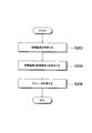
- FIG. 2 schematically shows an example of a skew measurement method for measuring the skew between output pins in the test apparatus 100.
- the wiring board 104 is prepared. That is, the first terminal 112, the second terminal 114, the first wiring 122 that connects the first terminal 112 and the binding node 116, and the second terminal 114 and the binding node 116 are connected to each other.
- a wiring substrate 104 having a second wiring 124 having a length equal to that of the wiring 122 and a third wiring 126 for connecting the binding node 116 and the output node is prepared.
- the test apparatus 100 and the wiring board 104 are coupled. That is, the first output pin 172 of the test apparatus 100 is coupled to the first terminal 112 of the wiring board 104, and the second output pin 174 of the test apparatus 100 is coupled to the second terminal 114 of the wiring board 104. Further, the input terminal 176 of the test apparatus 100 is coupled to the third terminal 118 of the wiring board 104.
- the skew between the first output pin 172 and the second output pin 174 is measured.
- the skew can be measured by measuring the voltage of the third terminal 118 in comparison with the reference voltage VREF .
- the test apparatus 100 may adjust the setting of the skew adjustment unit 140 based on the measured skew value so that the skew value falls within a predetermined range.
- FIG. 3 schematically shows an example of the method of measuring the skew of the test apparatus 100 described in relation to S206 of FIG.
- a first timing representing a transition timing of a signal obtained by outputting a test signal from the first output pin is measured.
- the first timing can be measured by the following procedure, for example.
- a test signal is output from the first output pin 172 with the second output pin 174 maintained at a high level or a low level.
- the voltage of the third terminal 118 of the wiring board 104 is input to one input terminal of the comparator 162 via the input terminal 176.
- the first reference voltage determined based on the relationship between the level of the second output pin 174 and the transition state of the test signal is input to the other input terminal of the comparator 162.
- the timing at which the voltage at the third terminal 118 matches the first reference voltage is measured as the first timing.
- the second timing representing the transition timing of the signal obtained by outputting the test signal from the second output pin is measured.
- the second timing can be measured by the following procedure, for example.
- a test signal is output from the second output pin 174 with the first output pin 172 maintained at a high level or a low level.
- the voltage of the third terminal 118 of the wiring board 104 is input to one input terminal of the comparator 162 via the input terminal 176.
- the second reference voltage determined based on the relationship between the level of the first output pin 172 and the transition state of the test signal is input to the other input terminal of the comparator 162.
- the timing at which the voltage at the third terminal 118 matches the second reference voltage is measured as the second timing.
- the skew between the first output pin 172 and the second output pin 174 is measured.
- the skew can be obtained from the difference between the first timing and the second timing.
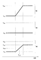
- FIG. 4 schematically shows an example of the first timing measurement process described in relation to FIG.
- FIG. 4 shows the output 42 of the first output pin 172, the output 44 of the second output pin 174, and the voltage 46 of the third terminal 118 input to the comparator 162 by solid lines.
- the voltages of the output 42 and the output 44 are expressed as voltages when the wiring board 104 is not coupled to the first output pin 172 and the second output pin 174, that is, voltages at the open end.
- the output resistors 152, 154, and termination resistors 166 have the same resistivity, and V low is applied as the voltage V TT .
- the first output pin 172 outputs a test signal that transitions from a low level V low to a high level V high .
- the output 44 of the second output pin 174 is maintained at the low level V low .
- the voltage 46 is input to one input terminal of the comparator 162.
- the value of the voltage 46 changes from V low to V high ′ .
- the first reference voltage V REF1 is input to the other input terminal of the comparator 162.
- the first timing T posi ′ is measured as the timing at which the voltage 46 matches the first reference voltage V REF1 .
- the value of the first reference voltage VREF1 for example, a value of 50% of the input amplitude is set.
- FIG. 5 schematically shows an example of the second timing measurement process described in relation to FIG.
- FIG. 5 shows in solid lines the output 42 of the first output pin 172, the output 44 of the second output pin 174, and the voltage 46 of the third terminal 118 input to the comparator 162.
- the voltages of the output 42 and the output 44 are expressed as voltages when the wiring board 104 is not coupled to the first output pin 172 and the second output pin 174, that is, voltages at the open end.
- the output resistors 152, 154, and termination resistors 166 have the same resistivity, and V low is applied as the voltage V TT .
- the second output pin 174 outputs a test signal that transitions from the high level V high to the low level V low .
- the output 42 of the first output pin 172 is maintained at the low level V low .
- the voltage 46 is input to one input terminal of the comparator 162.
- the value of the voltage 46 transitions from V high ′ to V low .
- the second reference voltage V REF2 is input to the other input terminal of the comparator 162.
- the second timing T nega ′ is measured as a timing at which the voltage 46 matches the second reference voltage V REF2 .
- As the value of the second reference voltage VREF2 for example, a value of 50% of the input amplitude is set.
- the test apparatus 100 may adjust the setting of the skew adjustment unit 140 so that the difference between the first timing T posi ′ and the second timing T negative ′ is within a predetermined range.
- the test apparatus 100 may adjust the setting of the skew adjustment unit 140 so as to be equal to the first timing T posi ′ and the second timing T negative ′ .
- FIG. 6 schematically shows another example of measuring the skew of the test apparatus 100.
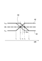
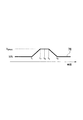
- FIG. 7 schematically shows an example of the spike voltage generated at the third terminal 118 described with reference to FIG. 6 and 7, when the first output pin 172 outputs the positive phase signal 62 of the test signal and the second output pin 174 outputs the negative phase signal 64 of the test signal, the third terminal 118 is used.
- a method for measuring skew and a method for calibrating the skew will be described with reference to the value of the spike voltage 76 generated in FIG.
- the positive phase signal 62 transitions from the low level V low to the high level V high from the time t 1 to the time t 4 .
- the anti-phase signal 64 has a skew and transitions from the high level V high to the low level V low from the time t 2 to the time t 5 .
- the transition timing of the normal phase signal 62 and the negative phase signal 64 can be measured using, for example, a value of 50% of the input amplitude. 6, the transition timing of the positive-phase signal 62, the transition timing of t 2, and the negative-phase signal 64 becomes t 4. Skew is determined as the difference between t 4 and t 2. In FIG. 6, a dotted line 68 indicates a reverse phase signal when there is no skew. The time t 3 indicates the time that the positive phase signal 62 and the phase signal 64 crosses.
- a spike voltage 76 appears at 118.
- the value of the spike voltage 76 until time t 1, showing 50% of the value of input amplitude. After time t 1 , it gradually increases, and shows a substantially constant value V SPIKE between time t 2 and time t 4 . Then, gradually decreases past the time t 4, return to 50% of the value of the input amplitude becomes time t 5.
- the skew can be measured by measuring the time during which the spike voltage 76 shows a substantially constant value V SPIKE .
- the test apparatus 100 may adjust the setting of the skew adjustment unit 140 so that the spike voltage 76 becomes a certain value or less.
- the test apparatus 100 may adjust the setting of the skew adjustment unit 140 so that the time during which the spike voltage is generated is equal to or less than a certain value.
- FIG. 8 schematically shows a configuration example of a test apparatus 800 including a wiring board 804 according to another embodiment.
- the test apparatus 800 includes an apparatus main body 802 and a wiring board 804, and has substantially the same configuration as the test apparatus 100.
- the apparatus main body 802 has substantially the same configuration as the apparatus main body 102.
- the wiring board 804 has substantially the same configuration as the wiring board 104. Therefore, the test apparatus 800, the apparatus main body 802, and the wiring board 804 will be described mainly with respect to the differences from the test apparatus 100, the apparatus main body 102, and the wiring board 104, and description of the other may be omitted.
- the apparatus main body 802 includes a reference clock generation unit 130 and a test execution unit 832.
- the test execution unit 832 includes a timing generation unit 134, a pattern generation unit 136, a waveform shaping unit 138, a skew adjustment unit 140, a differential driver 150, a first output pin 172, and a second output pin 174.
- the skew adjustment unit 140 includes a variable delay circuit 142 and a variable delay circuit 144.
- the differential driver 150 includes an output resistor 152 and an output resistor 154.
- the wiring board 804 includes a first terminal 112, a second terminal 114, a binding node 116, a first wiring 122, and a second wiring 124 for each of the plurality of test execution units 832.
- the wiring board 804 is different from the wiring board 104 in that it includes a multiplexer 810 and a broadband comparator circuit 820.
- the broadband comparator circuit 820 may be an example of a timing measurement circuit.
- the multiplexer 810 includes an output terminal 812 and a plurality of input terminals 818.
- the input terminal 818 of the multiplexer 810 may be an example of an output node.
- a binding node 116 corresponding to each of the plurality of test execution units 832 is connected to each of the input terminals 818.
- Multiplexer 810 selects a signal to be output from signals input to a plurality of input terminals 818 and supplies the selected signal to broadband comparator circuit 820.
- the wiring board 804 is different from the wiring board 104 in that the third wiring 126 connects the binding node 116 and the input terminal 818 of the multiplexer 810.
- the drawing of the connection relationship between the plurality of test execution units 832 and the plurality of binding nodes 116 is omitted.
- the broadband comparator circuit 820 corresponds to the comparator 162 of the test apparatus 100.
- the broadband comparator circuit 820 measures the transition timing of the signal supplied from the multiplexer 810.
- the wiring board 804 is described as using the input terminal 818 of the multiplexer 810 instead of the third terminal 118 as an output node, but the present invention is not limited to this.
- the output node may be the input node 828 of the broadband comparator circuit 820.
- the test apparatus 800 can measure the skew between the output pins even when the comparator is not mounted on the apparatus main body 802.
- the test apparatus 800 mounts the broadband comparator circuit 820 having higher accuracy than the comparator on the wiring board 804, so that the skew between the output pins is reduced. Can be measured accurately.
- the first signal and the second signal are generated by the same waveform shaping unit.
- the case where the first signal and the second signal are the positive phase signal and the negative phase signal of the same test signal has been described.
- the first signal and the second signal are not limited to this.
- the first signal and the second signal may be generated by different waveform shaping units.
- the second signal starts transition from the low level or the high level to the high level or the low level while the first signal transits from the high level or the low level to the low level or the high level. Good.
Landscapes
- Physics & Mathematics (AREA)
- General Physics & Mathematics (AREA)
- Engineering & Computer Science (AREA)
- General Engineering & Computer Science (AREA)
- Tests Of Electronic Circuits (AREA)
Abstract
Description
出願番号 12/199,811 出願日 2008年8月28日
VREF1 = (Vhigh'-Vlow)/2 ・・・(1)
Claims (10)
- 第1信号および第2信号を含む試験信号を被試験デバイスに与えて前記被試験デバイスを試験する試験装置における出力ピンの間のスキュー測定に用いられる配線基板であって、
前記第1信号を出力すべき第1出力ピンに結合される第1端子と、
前記第2信号を出力すべき第2出力ピンに結合される第2端子と、
前記第1端子および前記第2端子の双方に接続される結束ノードと、
入力される信号の遷移タイミングを計測するタイミング計測回路に接続される出力ノードと、
前記第1端子および前記結束ノードの間を接続する第1配線と、
前記第2端子および前記結束ノードの間を接続する第2配線と、
前記結束ノードおよび前記出力ノードの間を接続する第3配線と、
を備え、
前記第1配線および前記第2配線が等しい長さに形成された配線基板。 - 前記第1配線および前記第2配線が等しくかつ最短の長さに形成された、
請求項1に記載の配線基板。 - 前記試験装置は、前記タイミング計測回路と、前記タイミング計測回路に接続される入力端子とを備え、
前記出力ノードは、前記入力端子に結合される第3端子である、
請求項1または請求項2に記載の配線基板。 - 前記タイミング計測回路をさらに備え、
前記出力ノードは、前記タイミング計測回路の入力ノードである、
請求項1または請求項2に記載の配線基板。 - 前記第1出力ピンが出力する前記第1信号は前記試験信号の正相信号であり、前記第2出力ピンが出力する前記第2信号は前記試験信号の逆相信号である、
請求項1から請求項4までの何れか一項に記載の配線基板。 - 第1信号および第2信号を含む試験信号を被試験デバイスに与えて前記被試験デバイスを試験する試験装置における出力ピンの間のスキューを計測するスキュー測定方法であって、
請求項1から請求項5までの何れか一項に記載の配線基板を準備する段階と、
前記第1信号を出力する前記試験装置の前記第1出力ピンを、前記配線基板の前記第1端子に結合し、前記第2信号を出力する前記試験装置の前記第2出力ピンを、前記配線基板の前記第2端子に結合する段階と、
前記出力ノードの電圧を参照電圧との比較において計測することにより、前記第1出力ピンと前記第2出力ピンとの間のスキューを計測する段階と、
を備えたスキュー測定方法。 - 前記スキューを計測する段階は、
前記第2出力ピンをハイレベルまたはローレベルに維持した状態で、前記第1出力ピンから前記第1信号を出力し、前記出力ノードの電圧が、前記第2出力ピンのレベルと前記第1信号の遷移状態との関係に基づき決定される第1参照電圧に一致する第1タイミングを計測する段階と、
前記第1出力ピンをハイレベルまたはローレベルに維持した状態で、前記第2出力ピンから前記第2信号を出力し、前記出力ノードの電圧が、前記第1出力ピンのレベルと前記第2信号の遷移状態との関係に基づき決定される第2参照電圧に一致する第2タイミングを計測する段階と、
前記第1タイミングと前記第2タイミングとの差から前記スキューを計測する段階と、
を有する請求項6に記載のスキュー測定方法。 - 前記第1出力ピンは前記試験信号の正相信号を出力し、前記第2出力ピンは前記試験信号の逆相信号を出力し、
前記スキューを計測する段階は、
前記出力ノードに発生するスパイク電圧の値により前記スキューを計測する、
請求項6に記載のスキュー測定方法。 - 前記第1信号および前記第2信号は、それぞれ、同一の試験信号の正相信号および逆相信号であり、
前記スキューを計測する段階は、
前記同一の試験信号を出力する段階と、
前記出力ノードに発生するスパイク電圧の値により前記スキューを計測する、
請求項6に記載のスキュー測定方法。 - 第1信号および第2信号を含む試験信号を被試験デバイスに与えて前記被試験デバイスを試験する試験装置であって、
前記第1信号を出力する第1出力ピンと、
前記第2信号を出力する第2出力ピンと、
入力される信号のタイミングを計測するタイミング計測回路と、
請求項1から請求項5までの何れか一項に記載の配線基板と、
を備えた試験装置。
Priority Applications (3)
| Application Number | Priority Date | Filing Date | Title |
|---|---|---|---|
| KR1020117002957A KR101178069B1 (ko) | 2008-08-28 | 2009-08-27 | 상호 접속 기판, 스큐 측정 방법 및 시험 장치 |
| JP2010526555A JP5475666B2 (ja) | 2008-08-28 | 2009-08-27 | スキュー測定方法および試験装置 |
| CN200980133261.8A CN102132166B (zh) | 2008-08-28 | 2009-08-27 | 互连基板、偏差测定方法及测试装置 |
Applications Claiming Priority (2)
| Application Number | Priority Date | Filing Date | Title |
|---|---|---|---|
| US12/199,811 | 2008-08-28 | ||
| US12/199,811 US7768255B2 (en) | 2008-08-28 | 2008-08-28 | Interconnection substrate, skew measurement method, and test apparatus |
Publications (1)
| Publication Number | Publication Date |
|---|---|
| WO2010023924A1 true WO2010023924A1 (ja) | 2010-03-04 |
Family
ID=41721107
Family Applications (1)
| Application Number | Title | Priority Date | Filing Date |
|---|---|---|---|
| PCT/JP2009/004177 Ceased WO2010023924A1 (ja) | 2008-08-28 | 2009-08-27 | 相互接続基板、スキュー測定方法および試験装置 |
Country Status (5)
| Country | Link |
|---|---|
| US (1) | US7768255B2 (ja) |
| JP (1) | JP5475666B2 (ja) |
| KR (1) | KR101178069B1 (ja) |
| CN (1) | CN102132166B (ja) |
| WO (1) | WO2010023924A1 (ja) |
Cited By (3)
| Publication number | Priority date | Publication date | Assignee | Title |
|---|---|---|---|---|
| JP2011024204A (ja) * | 2009-07-17 | 2011-02-03 | Tektronix Inc | Tmds信号用差動スキュー効果の発生方法及び装置 |
| US8592415B2 (en) | 2009-02-11 | 2013-11-26 | Reaction Biology Corp. | Selective kinase inhibitors |
| US10045981B2 (en) | 2015-11-24 | 2018-08-14 | Jakpharm, Llc | Selective kinase inhibitors |
Families Citing this family (4)
| Publication number | Priority date | Publication date | Assignee | Title |
|---|---|---|---|---|
| JP5429727B2 (ja) * | 2007-08-24 | 2014-02-26 | ワイアイケー株式会社 | 半導体試験装置 |
| KR102415198B1 (ko) * | 2017-11-20 | 2022-07-04 | 에스케이하이닉스 주식회사 | 스큐 보상 회로 및 이를 포함하는 반도체 장치 |
| TWI647546B (zh) * | 2018-06-29 | 2019-01-11 | 志聖工業股份有限公司 | 防板偏檢知設計 |
| US11428732B2 (en) * | 2019-08-28 | 2022-08-30 | Keysight Technologies, Inc. | Self-calibrating deskew fixture |
Citations (6)
| Publication number | Priority date | Publication date | Assignee | Title |
|---|---|---|---|---|
| JPH0862291A (ja) * | 1994-08-24 | 1996-03-08 | Mitsubishi Denki Semiconductor Software Kk | 半導体試験装置のスキュー校正装置 |
| JPH0882655A (ja) * | 1994-09-13 | 1996-03-26 | Fujitsu Ltd | 集積回路試験装置 |
| JP2001021620A (ja) * | 1999-07-07 | 2001-01-26 | Mitsubishi Electric Corp | Lsi試験装置およびそのタイミングキャリブレーション方法 |
| JP2003043124A (ja) * | 2001-07-31 | 2003-02-13 | Advantest Corp | 試験装置、及びキャリブレーション方法 |
| JP2005293808A (ja) * | 2004-04-05 | 2005-10-20 | Advantest Corp | 試験装置、位相調整方法、及びメモリコントローラ |
| JP2005331264A (ja) * | 2004-05-18 | 2005-12-02 | Yokogawa Electric Corp | 半導体試験装置 |
Family Cites Families (7)
| Publication number | Priority date | Publication date | Assignee | Title |
|---|---|---|---|---|
| US4656178A (en) * | 1983-09-01 | 1987-04-07 | Junusov Sabir J | Pharmaceutical composition possessing antiarrhythmic effect |
| US4724378A (en) * | 1986-07-22 | 1988-02-09 | Tektronix, Inc. | Calibrated automatic test system |
| US6448799B1 (en) * | 1999-09-30 | 2002-09-10 | Hitachi Electronics Engineering Co., Ltd. | Timing adjustment method and apparatus for semiconductor IC tester |
| JP3562581B2 (ja) * | 2000-12-20 | 2004-09-08 | 日本電気株式会社 | スキュー調整回路及び半導体集積回路 |
| US7595629B2 (en) * | 2004-07-09 | 2009-09-29 | Formfactor, Inc. | Method and apparatus for calibrating and/or deskewing communications channels |
| DE102004036145A1 (de) * | 2004-07-26 | 2006-03-23 | Infineon Technologies Ag | Halbleiterschaltungseinrichtung und System zum Testen einer Halbleitervorrichtung |
| US7523007B2 (en) * | 2006-06-30 | 2009-04-21 | Teradyne, Inc. | Calibration device |
-
2008
- 2008-08-28 US US12/199,811 patent/US7768255B2/en active Active
-
2009
- 2009-08-27 CN CN200980133261.8A patent/CN102132166B/zh active Active
- 2009-08-27 JP JP2010526555A patent/JP5475666B2/ja active Active
- 2009-08-27 WO PCT/JP2009/004177 patent/WO2010023924A1/ja not_active Ceased
- 2009-08-27 KR KR1020117002957A patent/KR101178069B1/ko active Active
Patent Citations (6)
| Publication number | Priority date | Publication date | Assignee | Title |
|---|---|---|---|---|
| JPH0862291A (ja) * | 1994-08-24 | 1996-03-08 | Mitsubishi Denki Semiconductor Software Kk | 半導体試験装置のスキュー校正装置 |
| JPH0882655A (ja) * | 1994-09-13 | 1996-03-26 | Fujitsu Ltd | 集積回路試験装置 |
| JP2001021620A (ja) * | 1999-07-07 | 2001-01-26 | Mitsubishi Electric Corp | Lsi試験装置およびそのタイミングキャリブレーション方法 |
| JP2003043124A (ja) * | 2001-07-31 | 2003-02-13 | Advantest Corp | 試験装置、及びキャリブレーション方法 |
| JP2005293808A (ja) * | 2004-04-05 | 2005-10-20 | Advantest Corp | 試験装置、位相調整方法、及びメモリコントローラ |
| JP2005331264A (ja) * | 2004-05-18 | 2005-12-02 | Yokogawa Electric Corp | 半導体試験装置 |
Cited By (3)
| Publication number | Priority date | Publication date | Assignee | Title |
|---|---|---|---|---|
| US8592415B2 (en) | 2009-02-11 | 2013-11-26 | Reaction Biology Corp. | Selective kinase inhibitors |
| JP2011024204A (ja) * | 2009-07-17 | 2011-02-03 | Tektronix Inc | Tmds信号用差動スキュー効果の発生方法及び装置 |
| US10045981B2 (en) | 2015-11-24 | 2018-08-14 | Jakpharm, Llc | Selective kinase inhibitors |
Also Published As
| Publication number | Publication date |
|---|---|
| CN102132166A (zh) | 2011-07-20 |
| CN102132166B (zh) | 2014-04-09 |
| JP5475666B2 (ja) | 2014-04-16 |
| US7768255B2 (en) | 2010-08-03 |
| KR101178069B1 (ko) | 2012-08-30 |
| JPWO2010023924A1 (ja) | 2012-01-26 |
| KR20110034662A (ko) | 2011-04-05 |
| US20100052723A1 (en) | 2010-03-04 |
Similar Documents
| Publication | Publication Date | Title |
|---|---|---|
| JP5475666B2 (ja) | スキュー測定方法および試験装置 | |
| JP5279724B2 (ja) | 試験装置およびキャリブレーション方法 | |
| US6298465B1 (en) | Skew calibration means and a method of skew calibration | |
| US6784684B2 (en) | Testing apparatus including testing board having wirings connected to common point and method of testing semiconductor device by composing signals | |
| US10761130B1 (en) | Voltage driver circuit calibration | |
| KR101250498B1 (ko) | 출력 장치 및 시험 장치 | |
| KR20090082434A (ko) | 시험 장치, 드라이버 컴퍼레이터 칩, 응답 측정 장치, 교정 방법 및 교정 장치 | |
| KR100736680B1 (ko) | 반도체 소자 테스트 장치의 캘리브레이션 방법 | |
| WO2009087874A1 (ja) | 試験装置、プローブカード、および試験方法 | |
| KR100868995B1 (ko) | 시험 장치, 조정 장치, 조정 방법, 및 조정 프로그램을기록한 기록 매체 | |
| JPWO2010007770A1 (ja) | 試験装置 | |
| JP5038137B2 (ja) | 半導体試験装置 | |
| JPWO2007072738A1 (ja) | 試験装置、調整装置、調整方法、および、調整プログラム | |
| JP4846134B2 (ja) | 試験装置、及びキャリブレーション方法 | |
| KR100724089B1 (ko) | 반도체 시험 장치의 캘리브레이션 방법 및 반도체 시험장치 | |
| KR100193323B1 (ko) | 측정용 신호의 전파 지연 시간 측정 회로 및 측정방법 | |
| JP2012052835A (ja) | 波形発生装置および波形発生装置の配線遅延校正方法 | |
| CN111352060B (zh) | 一种时域反射计的特性阻抗时域双参考线校准方法 | |
| JP4714067B2 (ja) | キャリブレーション回路、キャリブレーション方法、及び試験装置 | |
| US20030016041A1 (en) | Method and apparatus for testing semiconductor integrated circuit, and semiconductor integrated circuit manufactured thereby | |
| JP2000346910A (ja) | Icの多数並列同時テスト用測定装置 | |
| CN121349253A (zh) | 延时值校准方法、装置及存储介质 | |
| CN120214542A (zh) | 一种用于测试芯片的测试系统和芯片测试方法 | |
| JP2008008759A (ja) | キャリブレーションボードセット、半導体試験装置およびキャリブレーション方法 | |
| JP2008045879A (ja) | コンパレータのスキュー測定方法 |
Legal Events
| Date | Code | Title | Description |
|---|---|---|---|
| WWE | Wipo information: entry into national phase |
Ref document number: 200980133261.8 Country of ref document: CN |
|
| 121 | Ep: the epo has been informed by wipo that ep was designated in this application |
Ref document number: 09809580 Country of ref document: EP Kind code of ref document: A1 |
|
| WWE | Wipo information: entry into national phase |
Ref document number: 2010526555 Country of ref document: JP |
|
| ENP | Entry into the national phase |
Ref document number: 20117002957 Country of ref document: KR Kind code of ref document: A |
|
| NENP | Non-entry into the national phase |
Ref country code: DE |
|
| 122 | Ep: pct application non-entry in european phase |
Ref document number: 09809580 Country of ref document: EP Kind code of ref document: A1 |