WO2009145259A1 - 白色光源、バックライト、液晶表示装置および照明装置 - Google Patents
白色光源、バックライト、液晶表示装置および照明装置 Download PDFInfo
- Publication number
- WO2009145259A1 WO2009145259A1 PCT/JP2009/059780 JP2009059780W WO2009145259A1 WO 2009145259 A1 WO2009145259 A1 WO 2009145259A1 JP 2009059780 W JP2009059780 W JP 2009059780W WO 2009145259 A1 WO2009145259 A1 WO 2009145259A1
- Authority
- WO
- WIPO (PCT)
- Prior art keywords
- phosphor
- light source
- white light
- light emitting
- phosphor layer
- Prior art date
- Legal status (The legal status is an assumption and is not a legal conclusion. Google has not performed a legal analysis and makes no representation as to the accuracy of the status listed.)
- Ceased
Links
Images

Classifications
-
- H—ELECTRICITY
- H10—SEMICONDUCTOR DEVICES; ELECTRIC SOLID-STATE DEVICES NOT OTHERWISE PROVIDED FOR
- H10H—INORGANIC LIGHT-EMITTING SEMICONDUCTOR DEVICES HAVING POTENTIAL BARRIERS
- H10H20/00—Individual inorganic light-emitting semiconductor devices having potential barriers, e.g. light-emitting diodes [LED]
- H10H20/80—Constructional details
- H10H20/85—Packages
- H10H20/851—Wavelength conversion means
- H10H20/8516—Wavelength conversion means having a non-uniform spatial arrangement or non-uniform concentration, e.g. patterned wavelength conversion layer or wavelength conversion layer with a concentration gradient
-
- C—CHEMISTRY; METALLURGY
- C09—DYES; PAINTS; POLISHES; NATURAL RESINS; ADHESIVES; COMPOSITIONS NOT OTHERWISE PROVIDED FOR; APPLICATIONS OF MATERIALS NOT OTHERWISE PROVIDED FOR
- C09K—MATERIALS FOR MISCELLANEOUS APPLICATIONS, NOT PROVIDED FOR ELSEWHERE
- C09K11/00—Luminescent materials, e.g. electroluminescent or chemiluminescent
- C09K11/08—Luminescent materials, e.g. electroluminescent or chemiluminescent containing inorganic luminescent materials
- C09K11/0883—Arsenides; Nitrides; Phosphides
-
- C—CHEMISTRY; METALLURGY
- C09—DYES; PAINTS; POLISHES; NATURAL RESINS; ADHESIVES; COMPOSITIONS NOT OTHERWISE PROVIDED FOR; APPLICATIONS OF MATERIALS NOT OTHERWISE PROVIDED FOR
- C09K—MATERIALS FOR MISCELLANEOUS APPLICATIONS, NOT PROVIDED FOR ELSEWHERE
- C09K11/00—Luminescent materials, e.g. electroluminescent or chemiluminescent
- C09K11/08—Luminescent materials, e.g. electroluminescent or chemiluminescent containing inorganic luminescent materials
- C09K11/77—Luminescent materials, e.g. electroluminescent or chemiluminescent containing inorganic luminescent materials containing rare earth metals
- C09K11/7728—Luminescent materials, e.g. electroluminescent or chemiluminescent containing inorganic luminescent materials containing rare earth metals containing europium
- C09K11/7734—Aluminates
-
- C—CHEMISTRY; METALLURGY
- C09—DYES; PAINTS; POLISHES; NATURAL RESINS; ADHESIVES; COMPOSITIONS NOT OTHERWISE PROVIDED FOR; APPLICATIONS OF MATERIALS NOT OTHERWISE PROVIDED FOR
- C09K—MATERIALS FOR MISCELLANEOUS APPLICATIONS, NOT PROVIDED FOR ELSEWHERE
- C09K11/00—Luminescent materials, e.g. electroluminescent or chemiluminescent
- C09K11/08—Luminescent materials, e.g. electroluminescent or chemiluminescent containing inorganic luminescent materials
- C09K11/77—Luminescent materials, e.g. electroluminescent or chemiluminescent containing inorganic luminescent materials containing rare earth metals
- C09K11/7728—Luminescent materials, e.g. electroluminescent or chemiluminescent containing inorganic luminescent materials containing rare earth metals containing europium
- C09K11/77342—Silicates
-
- C—CHEMISTRY; METALLURGY
- C09—DYES; PAINTS; POLISHES; NATURAL RESINS; ADHESIVES; COMPOSITIONS NOT OTHERWISE PROVIDED FOR; APPLICATIONS OF MATERIALS NOT OTHERWISE PROVIDED FOR
- C09K—MATERIALS FOR MISCELLANEOUS APPLICATIONS, NOT PROVIDED FOR ELSEWHERE
- C09K11/00—Luminescent materials, e.g. electroluminescent or chemiluminescent
- C09K11/08—Luminescent materials, e.g. electroluminescent or chemiluminescent containing inorganic luminescent materials
- C09K11/77—Luminescent materials, e.g. electroluminescent or chemiluminescent containing inorganic luminescent materials containing rare earth metals
- C09K11/7728—Luminescent materials, e.g. electroluminescent or chemiluminescent containing inorganic luminescent materials containing rare earth metals containing europium
- C09K11/77348—Silicon Aluminium Nitrides or Silicon Aluminium Oxynitrides
-
- C—CHEMISTRY; METALLURGY
- C09—DYES; PAINTS; POLISHES; NATURAL RESINS; ADHESIVES; COMPOSITIONS NOT OTHERWISE PROVIDED FOR; APPLICATIONS OF MATERIALS NOT OTHERWISE PROVIDED FOR
- C09K—MATERIALS FOR MISCELLANEOUS APPLICATIONS, NOT PROVIDED FOR ELSEWHERE
- C09K11/00—Luminescent materials, e.g. electroluminescent or chemiluminescent
- C09K11/08—Luminescent materials, e.g. electroluminescent or chemiluminescent containing inorganic luminescent materials
- C09K11/77—Luminescent materials, e.g. electroluminescent or chemiluminescent containing inorganic luminescent materials containing rare earth metals
- C09K11/7728—Luminescent materials, e.g. electroluminescent or chemiluminescent containing inorganic luminescent materials containing rare earth metals containing europium
- C09K11/7737—Phosphates
- C09K11/7738—Phosphates with alkaline earth metals
-
- C—CHEMISTRY; METALLURGY
- C09—DYES; PAINTS; POLISHES; NATURAL RESINS; ADHESIVES; COMPOSITIONS NOT OTHERWISE PROVIDED FOR; APPLICATIONS OF MATERIALS NOT OTHERWISE PROVIDED FOR
- C09K—MATERIALS FOR MISCELLANEOUS APPLICATIONS, NOT PROVIDED FOR ELSEWHERE
- C09K11/00—Luminescent materials, e.g. electroluminescent or chemiluminescent
- C09K11/08—Luminescent materials, e.g. electroluminescent or chemiluminescent containing inorganic luminescent materials
- C09K11/77—Luminescent materials, e.g. electroluminescent or chemiluminescent containing inorganic luminescent materials containing rare earth metals
- C09K11/7783—Luminescent materials, e.g. electroluminescent or chemiluminescent containing inorganic luminescent materials containing rare earth metals containing two or more rare earth metals one of which being europium
- C09K11/7784—Chalcogenides
- C09K11/7787—Oxides
- C09K11/7789—Oxysulfides
-
- H—ELECTRICITY
- H10—SEMICONDUCTOR DEVICES; ELECTRIC SOLID-STATE DEVICES NOT OTHERWISE PROVIDED FOR
- H10H—INORGANIC LIGHT-EMITTING SEMICONDUCTOR DEVICES HAVING POTENTIAL BARRIERS
- H10H20/00—Individual inorganic light-emitting semiconductor devices having potential barriers, e.g. light-emitting diodes [LED]
- H10H20/80—Constructional details
- H10H20/85—Packages
- H10H20/852—Encapsulations
- H10H20/853—Encapsulations characterised by their shape
-
- G—PHYSICS
- G02—OPTICS
- G02F—OPTICAL DEVICES OR ARRANGEMENTS FOR THE CONTROL OF LIGHT BY MODIFICATION OF THE OPTICAL PROPERTIES OF THE MEDIA OF THE ELEMENTS INVOLVED THEREIN; NON-LINEAR OPTICS; FREQUENCY-CHANGING OF LIGHT; OPTICAL LOGIC ELEMENTS; OPTICAL ANALOGUE/DIGITAL CONVERTERS
- G02F1/00—Devices or arrangements for the control of the intensity, colour, phase, polarisation or direction of light arriving from an independent light source, e.g. switching, gating or modulating; Non-linear optics
- G02F1/01—Devices or arrangements for the control of the intensity, colour, phase, polarisation or direction of light arriving from an independent light source, e.g. switching, gating or modulating; Non-linear optics for the control of the intensity, phase, polarisation or colour
- G02F1/13—Devices or arrangements for the control of the intensity, colour, phase, polarisation or direction of light arriving from an independent light source, e.g. switching, gating or modulating; Non-linear optics for the control of the intensity, phase, polarisation or colour based on liquid crystals, e.g. single liquid crystal display cells
- G02F1/133—Constructional arrangements; Operation of liquid crystal cells; Circuit arrangements
- G02F1/1333—Constructional arrangements; Manufacturing methods
- G02F1/1335—Structural association of cells with optical devices, e.g. polarisers or reflectors
- G02F1/1336—Illuminating devices
- G02F1/133617—Illumination with ultraviolet light; Luminescent elements or materials associated to the cell
-
- H—ELECTRICITY
- H10—SEMICONDUCTOR DEVICES; ELECTRIC SOLID-STATE DEVICES NOT OTHERWISE PROVIDED FOR
- H10H—INORGANIC LIGHT-EMITTING SEMICONDUCTOR DEVICES HAVING POTENTIAL BARRIERS
- H10H20/00—Individual inorganic light-emitting semiconductor devices having potential barriers, e.g. light-emitting diodes [LED]
- H10H20/80—Constructional details
- H10H20/85—Packages
- H10H20/851—Wavelength conversion means
- H10H20/8511—Wavelength conversion means characterised by their material, e.g. binder
- H10H20/8512—Wavelength conversion materials
- H10H20/8513—Wavelength conversion materials having two or more wavelength conversion materials
-
- Y—GENERAL TAGGING OF NEW TECHNOLOGICAL DEVELOPMENTS; GENERAL TAGGING OF CROSS-SECTIONAL TECHNOLOGIES SPANNING OVER SEVERAL SECTIONS OF THE IPC; TECHNICAL SUBJECTS COVERED BY FORMER USPC CROSS-REFERENCE ART COLLECTIONS [XRACs] AND DIGESTS
- Y02—TECHNOLOGIES OR APPLICATIONS FOR MITIGATION OR ADAPTATION AGAINST CLIMATE CHANGE
- Y02B—CLIMATE CHANGE MITIGATION TECHNOLOGIES RELATED TO BUILDINGS, e.g. HOUSING, HOUSE APPLIANCES OR RELATED END-USER APPLICATIONS
- Y02B20/00—Energy efficient lighting technologies, e.g. halogen lamps or gas discharge lamps
Definitions
- the present invention relates to a white light source using a light emitting diode, and a backlight, a liquid crystal display device and an illumination device using the white light source.
- a white light source using a light emitting diode is known.
- a white light source using an LED is one in which a phosphor layer in which a phosphor and a transparent resin are mixed is formed on a light emitting surface of an LED chip, and white light is obtained by combining the emission color of the LED chip and the emission color of the phosphor.
- Patent Document 1 discloses a white light source in which a blue LED having an emission peak of 420 to 490 nm and a yellow phosphor are combined.
- the white light obtained from this white light source has high luminance, it has a problem that it is a pseudo white color having a slightly yellowish color and has poor color reproducibility.
- Patent Document 2 discloses an ultraviolet light emitting diode having an emission peak of 370 to 410 nm, a blue phosphor, a green phosphor, and a red phosphor. A combination of phosphor layers containing benzene has been proposed. According to this white light source, since blue phosphor, green phosphor, and red phosphor are used, the color reproducibility is improved and clean white light can be obtained.
- the white light source described in Patent Document 2 improves the color reproducibility of white light by combining an ultraviolet light-emitting diode with a blue phosphor, a green phosphor, and a red phosphor, 3 in the phosphor layer. Since various types of phosphors are mixed, there is a problem that it is difficult to adjust the dispersion state of the phosphors and the light distribution is poor.
- the white light source described in Patent Document 2 can improve the problem of light distribution by using a reflector as described in Patent Document 2, so that the problem of light distribution can be improved.
- the structure in which the phosphor layer is provided is employed, the light distribution varies. As described above, when the light distribution of the white light source varies, there is a problem in that the color unevenness of the white light occurs when a backlight or a lighting device is configured using a plurality of white light sources.
- the present invention has been made in view of the above circumstances, and provides a white light source having good light distribution, and a backlight, a liquid crystal display device, and an illumination device in which color unevenness is improved by using the white light source. For the purpose.
- the present invention has been completed by finding that a white light source with good light distribution can be obtained when the phosphor layer of the white light source satisfies a predetermined condition.
- the white light source solves the above problems, and includes an insulating substrate, a light emitting diode chip that is disposed on the insulating substrate and generates ultraviolet light having a wavelength of 330 nm to 410 nm, and the light emitting diode.
- a phosphor layer that is formed so as to cover the chip and contains a red light-emitting phosphor, a green light-emitting phosphor, and a blue light-emitting phosphor as a phosphor, and the phosphor is dispersed in a transparent resin cured product.
- the backlight according to the present invention solves the above-mentioned problems and is characterized by using the white light source.
- a liquid crystal display device solves the above-mentioned problems, and is characterized by comprising the backlight.
- an illumination device solves the above-described problems, and is characterized by using the white light source.
- the white light source according to the present invention has good light distribution.
- the backlight, liquid crystal display device and illumination device according to the present invention have little color unevenness.
- Sectional drawing which shows an example of the white light source which concerns on this invention.
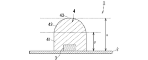
- FIG. 1 is a sectional view showing an example of the white light source of the present invention.
- 1 is a white light source
- 2 is an insulating substrate
- 3 is an LED chip
- 4 is a phosphor layer
- x is the height of the phosphor layer
- y is the height of the body of the phosphor layer.
- the insulating substrate 2 is a substrate having electrical insulation. Examples of the insulating substrate 2 include a ceramic substrate and a printed substrate. The insulating substrate 2 is provided with wirings for electrical connection with the LED chip 3 at necessary places.
- An LED chip 3 is disposed on the insulating substrate 2.
- the LED chip (light emitting diode chip) 3 is a light emitting diode chip that generates ultraviolet light having an emission peak of 330 nm to 410 nm.
- the shape of the LED chip 3 is not particularly limited.
- the emission peak of the light emitting diode chip is less than 330 nm, the emission peak is different from the excitation wavelength region of the phosphor, so that it is necessary to separately adjust the phosphor, and the ultraviolet rays become too strong, which may adversely affect the human body. .
- the light emission peak of the light emitting diode chip exceeds 410 nm, blue becomes too strong and the light emission peak is different from the excitation wavelength region of the phosphor, so that there is a possibility that the phosphor needs to be adjusted separately.
- the phosphor layer 4 is formed so as to cover the light-emitting diode chip 3, and contains a red light-emitting phosphor, a green light-emitting phosphor, and a blue light-emitting phosphor as the phosphor, and the phosphor is dispersed in the cured transparent resin. It will be.
- the phosphor dispersed in the phosphor layer 4 at least three kinds of phosphors of a red light emitting phosphor, a green light emitting phosphor and a blue light emitting phosphor are used.
- any phosphor can be used as long as it emits blue, green, and red light with light having an excitation wavelength of 330 nm to 410 nm. However, considering aspects such as color rendering properties and luminance characteristics, the following phosphors are desirable.
- Red phosphor powder As the red phosphor powder, a red phosphor powder that emits red light having a peak wavelength of 620 nm or more and 780 nm or less by light having an excitation wavelength of 330 nm to 410 nm is used.
- the red phosphor powder include a red phosphor powder made of europium-activated lanthanum oxysulfide having a composition represented by the following formula (2), and a red phosphor powder having a composition represented by the following formula (3) The powder which consists of at least 1 sort (s) of these is used.
- M is at least one element selected from Sb, Sm, Ga and Sn
- x and y are values satisfying 0.01 ⁇ x ⁇ 0.15 and 0 ⁇ y ⁇ 0.03.
- M in Formula (2) is at least one element selected from Sb, Sm, Ga, and Sn because the luminous efficiency of the red phosphor powder is high.
- x in the formula (3) is in the above range because the wavelength range of light emitted from the red phosphor powder is appropriate, the emission efficiency is high, and the balance between the wavelength range and the emission efficiency is good.
- the light emitted from the red phosphor powder tends to have a shorter wavelength as x in formula (3) increases within the above range, and the emission efficiency of the red phosphor powder tends to increase as it decreases within the above range.
- Green phosphor powder As the green phosphor powder, a green phosphor powder that emits green light having a peak wavelength of 490 nm to 575 nm by light having an excitation wavelength of 330 nm to 410 nm is used.
- Examples of the green phosphor powder include at least one of europium manganese activated aluminate having a composition represented by the following formula (4) and a green phosphor powder having a composition represented by the following formula (5). Powder is used.
- y in the formula (5) is in the above range because Mn is sufficiently dissolved in the green phosphor powder.
- z in the formula (5) is in the above range because the green phosphor powder has high luminous efficiency.
- u in the formula (5) is within the above range because the wavelength of light emitted from the green phosphor powder is suitable for illumination and backlight. Further, as u in the formula (5) increases within the above range, the wavelength of light emitted from the green phosphor powder becomes longer and more suitable for illumination.
- Blue phosphor powder As the blue phosphor powder, a blue phosphor powder that emits blue light having a peak wavelength of 430 nm to 460 nm by light having an excitation wavelength of 330 nm to 410 nm is used. As the blue phosphor powder, for example, a blue phosphor powder having a composition represented by the following formula (6) is used.
- x and y in formula (6) increase within the above ranges, the light emission component of the long wavelength of the light emitted from the blue phosphor powder increases, so that the white LED lamp becomes more suitable for lighting applications. Further, as x and y in the formula (6) become smaller within the above ranges, the spectrum width of light emitted from the blue phosphor powder becomes narrower, so that the white LED lamp becomes more suitable for backlight use. It is preferable that z in the formula (6) is in the above range because the luminous efficiency of the blue phosphor powder is high.
- red light-emitting phosphors, green light-emitting phosphors and blue light-emitting phosphors are appropriately selected in consideration of the color rendering properties, the uniformity of light emission, and the luminance characteristics of the white light source 1, and the types of the phosphors to be blended are appropriately selected. Change the amount.
- the phosphor dispersed in the phosphor layer 4 emits yellow or orange light with an excitation wavelength of 330 nm to 410 nm in addition to the red light emitting phosphor, the green light emitting phosphor and the blue light emitting phosphor.
- a phosphor may be used.
- the phosphor dispersed in the phosphor layer 4 preferably has an average particle size of 10 ⁇ m to 60 ⁇ m.
- the average particle size is meant the cumulative 50% particle diameter D 50.
- the average particle diameter is less than 10 ⁇ m, the phosphor particles are too fine, and when the average particle diameter exceeds 60 ⁇ m, the phosphor particles are too large, so that t / L is adjusted to t / L ⁇ 3.2, respectively. Becomes difficult.
- the transparent resin cured product of the phosphor layer 4 is obtained by curing a transparent resin.
- the transparent resin can be used without particular limitation as long as it is transparent.
- a silicone resin or an epoxy resin is used.
- the phosphor content in the phosphor layer 4 is preferably 20% by mass to 80% by mass.
- the content of the phosphor means the mass ratio of the phosphor in the total mass of the phosphor and the transparent resin cured product.
- the white light source 1 becomes large and is not suitable for practical use. .
- the phosphor content exceeds 80% by mass, it may be difficult to uniformly mix and apply the phosphors of the respective colors. If the phosphor content exceeds 90% by mass, the light from the light emitting diode may not be uniformly transmitted into the phosphor layer.
- the phosphor layer 4 is formed so as to cover the portion including the side surface of the LED chip 3.
- the phosphor layer 4 covers the portion including the side surface of the LED chip 3 because the light distribution of the white light source 1 is improved.
- the phosphor layer 4 may be formed so as to cover only the light emitting surface of the LED chip 3.
- the shortest distance between the surface of the phosphor layer 4 and the outer peripheral portion of the light emitting diode chip 3 is t (mm), and the mean free path defined by the following formula (1) is L (mm).
- L 1 / (n ⁇ ⁇ ) (1)
- N number of phosphors per unit volume of phosphor layer (pcs / mm 3 )
- ⁇ average cross-section area of phosphors in phosphor layer (mm 2 )
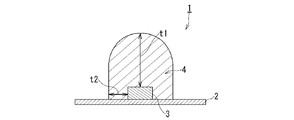
- the shortest distance t (mm) between the surface of the phosphor layer and the outer peripheral portion of the light emitting diode chip means the shortest distance among the distances between the arbitrary outer peripheral end of the LED chip 3 and the surface of the phosphor layer 4. To do. In other words, t indicates the minimum thickness of the phosphor layer.
- an arbitrary outer peripheral end of the LED chip 3 may be a cross-sectional corner.
- FIG. 2 is a diagram for explaining a method of measuring the shortest distance t. As shown in FIG. 2, when distances t1, t2, etc. from the outer peripheral edge of the LED chip to the surface of the phosphor layer are obtained, if t2 is the shortest distance, this t2 becomes the shortest distance t.
- the shortest distance t is for obtaining the shortest thickness of the phosphor layer 4. For this reason, when the coating layer which consists of transparent resin hardened material etc. and does not contain fluorescent substance is further provided in the surface of the fluorescent substance layer 4, the thickness of this coating layer is not used for calculation of the shortest distance t.
- the mean free path L (mm) is an index indicating the separation distance of the phosphors dispersed in the phosphor layer, and is defined by the above formula (1).
- n is the number of phosphors per unit volume (pcs / mm 3 )
- ⁇ is the average cross section area (mm 2 ).
- the number of phosphors n per unit volume is the number of phosphors per 1 mm 3 in the phosphor layer.
- the number n of phosphors per unit volume is used when it can be directly measured, but may be simply calculated by the following method.
- a cubic piece having a unit volume of 400 ⁇ m ⁇ 400 ⁇ m ⁇ 400 ⁇ m is extracted from the phosphor layer.
- one surface of 400 ⁇ m ⁇ 400 ⁇ m is arbitrarily selected from the surface of the cube piece (hereinafter referred to as a first surface), and the number of phosphors in the first surface is measured by image analysis to determine the area per unit area. The number of phosphors N1 is obtained.
- one arbitrary surface is selected from the four surfaces perpendicular to the first surface (hereinafter referred to as the second surface), and the side joining the first surface and the second surface (hereinafter referred to as the first side).
- N7 (N2 + N3 + N4 + N5 + N6) / 5.
- the average cross section area ⁇ (mm 2 ) is an average value of the projected areas of the phosphors in the phosphor layer, calculated on the assumption that the phosphor is a true sphere.
- a specific method of calculating the average cross section area ⁇ (mm 2 ) is as follows. That is, first, the average particle diameter r1 of the phosphor is obtained from the particle size distribution of the phosphor in the phosphor layer, and the average volume of the phosphor is obtained from the average particle diameter r1. Next, the radius r2 of the phosphor when the phosphor is assumed to be a true sphere is calculated from the average volume of the phosphor. Further, a projected area of a perfect circle of the phosphor assumed to be a true sphere is calculated from the radius r2 of the phosphor, and this projected area is defined as an average cross section area ⁇ (mm 2 ).
- T / L is an index indicating the dispersion state of the phosphor in the phosphor layer.
- the dispersion state of the phosphors in the phosphor layer is good, and the distance at which the phosphors are easily reflected is maintained, so that scattering occurs effectively in the phosphor layer. For this reason, the white light distribution of the white light source is improved, and the variation in the light distribution is also reduced.
- t / L is preferably 3.2 ⁇ t / L ⁇ 6, and more preferably 3.5 ⁇ t / L ⁇ 5.5.
- the phosphor layer 4 includes a columnar first shape portion 41 formed on the insulating substrate 2 side, and a dome-shaped second shape portion 42 formed continuously at the end of the first shape portion 41. It is a cylindrical body having a dome-shaped end surface 43. That is, the outer shape of the phosphor layer 4 is formed in a so-called bullet shape. It is preferable that the phosphor layer 4 is formed in a bullet shape because the light emission of the white light source 1 tends to be uniform.
- the axial length of the first shape portion 41 is usually 10% or more, preferably 10% to 95%, with respect to the axial length of the entire phosphor layer 4. If the ratio of the axial length of the first shape portion 41 to the axial length of the entire phosphor layer 4 is within this range, it is desirable because the light emission of the white light source 1 tends to be uniform.
- FIG. 1 shows the axial length of the entire phosphor layer 4 as x and the axial length of the cylindrical first shape portion 41 as y.
- the length y in the axial direction of the first shape portion 41 is set to the axial length x of the entire phosphor layer 4, that is, y / x is usually 0. It is 5% or more, preferably 10% or more, and more preferably 10% to 95%.
- the phosphor layer has a mountain shape.
- the entire phosphor layer surface or the surface of the phosphor layer is formed. Many of them are curved and refracted when the light exits the phosphor layer, so that the optical path of the light emitted from the white light source tends to be uneven.
- the phosphor layer has a rod shape.
- y / x 100%
- y / x more than 95% and less than 100%
- the phosphor layer 4 shown in FIG. 1 is an example in which the phosphor layer is formed in a cannonball shape, but the phosphor layer of the white light source of the present invention is not limited to a cannonball shape, and may have any shape. Can be formed.
- the white light source of the present invention can be manufactured, for example, by mounting a light emitting diode chip on an insulating substrate and then forming a phosphor layer on the insulating substrate.
- the phosphor layer is formed on the insulating substrate by, for example, preparing a paste raw material, preparing a phosphor paste composition, and applying and drying the phosphor paste composition as follows.
- a paste material containing a phosphor and a transparent resin is prepared.
- the paste material is obtained by mixing the phosphor and the transparent resin using a known stirrer or the like.
- the paste raw material is preferably prepared so as to have a high phosphor content and a relatively high viscosity.
- the paste raw material is dispersed to prepare a phosphor paste composition in which the phosphor is sufficiently dispersed in the transparent resin.
- the phosphor paste composition can be obtained by dispersing the paste raw material using a mixing and dispersing apparatus.
- a known mixing / dispersing device can be used, but a roll type disperser is preferable because an appropriate compressive force and shearing force can be applied to the paste raw material.
- a roll-type disperser has a plurality of rolls with different rotational speeds, and passes through a gap between the rolls using a compression action using pressure between rolls and a shearing action between rolls with different speeds.
- a dispersion process is performed on a medium to be dispersed such as a paste raw material.
- a three roll mill is more preferable.
- the roll is made of a fine ceramic such as alumina, silicon nitride, silicon carbide, or the like, since impurities are hardly mixed into a medium to be dispersed such as a paste raw material. Further, among the rolls made of fine ceramic, a roll made of high alumina (high purity alumina having a purity of 99% or more) is more preferable because impurities are further less mixed.
- the phosphor paste composition obtained by carrying out the dispersion treatment is preferably subjected to defoaming / stirring treatment using a defoaming stirrer if necessary, because air in the phosphor paste composition is sufficiently deaerated.
- a defoaming stirrer a container for storing an object to be treated such as a phosphor paste composition is placed eccentrically on a rotating table, and the container itself is rotated so that the container rotates and revolves. The thing whose revolution is possible in reduced pressure is mentioned.
- the phosphor paste composition obtained by carrying out the dispersion treatment and the defoaming / stirring treatment can be obtained with a more uniform phosphor paste composition by performing the dispersion treatment again using the above-described dispersing device, if necessary. preferable.
- the phosphor paste composition has a high viscosity within a range in which phosphor particles can be dispersed because a phosphor layer having a high phosphor filling rate can be formed.
- the viscosity of the phosphor paste composition is preferably 3000 Pa ⁇ s to 10,000 Pa ⁇ s.
- the phosphor paste composition may be mixed with an organic solvent or a binder resin.
- the addition amount of the organic solvent and the binder resin is appropriately adjusted so that the viscosity and phosphor content of the phosphor paste composition to be finally obtained become a desired value.
- Addition of an organic solvent, a binder resin, or the like to the phosphor paste composition can be obtained by dispersing the phosphor paste composition to which an organic solvent, a binder resin, or the like has been added, using a dispersing device.
- a dispersing device used for adding an organic solvent, a binder resin, and the like include a homogenizer, a disper, a propeller type stirrer, a kneader, a planetary mixer, a mortar, a bamboo spatula, and the like.
- an insulating substrate on which the LED chip is mounted is prepared, and a phosphor paste composition is applied so as to cover the LED chip on the insulating substrate and dried to form a phosphor layer on the insulating substrate. To do.
- a current-carrying wiring may be provided on the LED chip by wire bonding or the like.
- the phosphor layer may be formed so as to cover one LED chip with one phosphor layer, or may be formed so as to cover a plurality of LED chips with one phosphor layer. Good.
- the white light source according to the present invention Since the white light source according to the present invention has a good light distribution, there is little variation in light emission. For this reason, when the white light source according to the present invention is used for a planar light source such as a backlight, a planar light source with little variation in light emission can be obtained. In addition, the white light source according to the present invention is suitable for a lighting device because it has a good light distribution and little light emission variation.
- the backlight according to the present invention uses the white light source according to the present invention.
- the backlight according to the present invention can be produced by a known method using the white light source.
- the backlight according to the present invention is a planar light source with little variation in light emission. Therefore, the backlight according to the present invention is suitable for a liquid crystal display device such as a television or a personal computer display.
- the liquid crystal display device includes the backlight according to the present invention.
- the liquid crystal display device according to the present invention can be manufactured by a known method using the backlight.
- the liquid crystal display device according to the present invention has little variation in light emission of the backlight. For this reason, the liquid crystal display device according to the present invention is suitable for applications such as televisions and personal computer displays.
- the lighting device according to the present invention uses the white light source according to the present invention.
- the lighting device according to the present invention can be manufactured by a known method using the white light source.
- the illuminating device according to the present invention has little light emission variation of the white light source. For this reason, the lighting device according to the present invention is suitable as a lighting device for home use, business use, and the like.
- Example 1 Light-emitting diode chip mounting
- an aluminum nitride insulating substrate thermal conductivity: 220 W / m ⁇ K
- a plurality of square metal patterns composed of Ti / Pt / Au layers are sequentially formed on the surface. Individually formed.
- the aluminum nitride insulating substrate was structured to conduct to the back surface side through a through hole, and an electrode pad was formed on the back surface of the substrate.
- one light emitting diode chip (LED chip) that emits ultraviolet light having an excitation wavelength of 390 nm was bonded to each metal pattern one by one, and the lower electrode of the light emitting diode chip and the metal pattern were electrically connected to each other. Further, the upper electrode of the light emitting diode chip and another metal pattern adjacent to the metal pattern on which the light emitting diode chip is mounted are electrically connected by a conductive wire using a bonding wire method.
- the size of the light-emitting diode chip is 0.36 mm long ⁇ 0.36 mm wide ⁇ 0.2 mm high.
- the phosphor layer was formed on the insulating substrate on which the light emitting diode chip was mounted by the following procedure.
- a blue phosphor, a green phosphor, a red phosphor, and a silicone resin were mixed using a mixing stirrer to prepare a paste raw material.
- the paste raw material was dispersed for 8 hours using a three-roll mill equipped with a high alumina roll (first dispersion treatment). After the first dispersion treatment, the paste material was defoamed at 5 mTorr for 10 minutes using a defoaming stirrer (first defoaming treatment). After the first defoaming treatment, the paste raw material was dispersed under the same conditions as the first dispersion treatment (second dispersion treatment). After the second dispersion treatment, the paste raw material was defoamed under the same conditions as the first defoaming treatment (second defoaming treatment).
- the paste material was dispersed under the same conditions as the first dispersion treatment (third dispersion treatment). After the third dispersion treatment, a phosphor paste composition was obtained.
- the phosphor paste composition had a viscosity of 6000 Pa ⁇ s.
- ⁇ Application and drying of phosphor paste composition Prepare an insulating substrate on which a light-emitting diode chip is mounted, apply a phosphor paste composition to cover the light-emitting diode chip on this insulating substrate, and dry it to form a phosphor layer on the insulating substrate did.
- the phosphor layer was formed in a bullet shape as shown in FIG. A white light source was obtained by forming the phosphor layer.
- the resulting white light source was measured for light distribution.
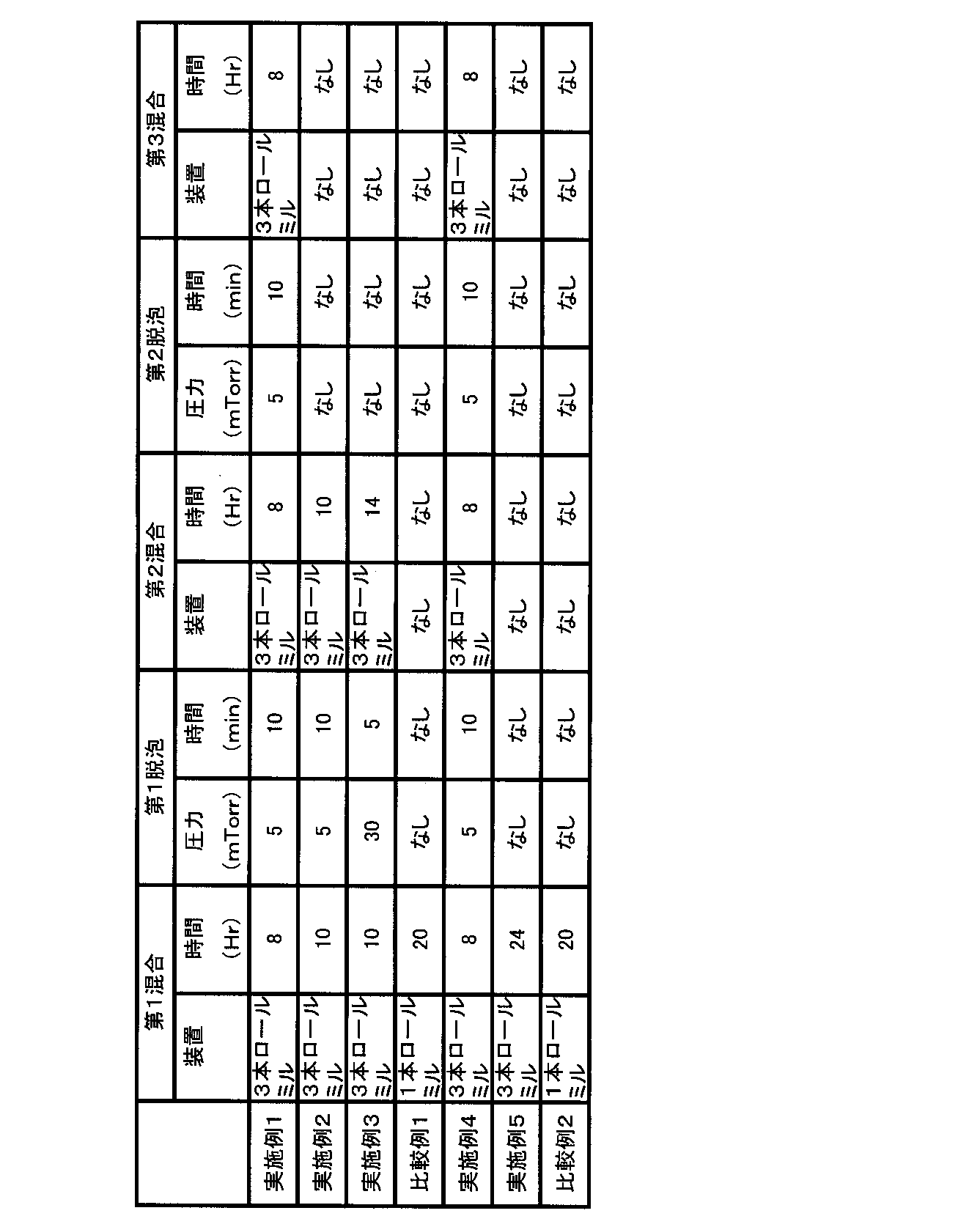
- Tables 1 and 2 show the manufacturing conditions of the white light source.
- Table 2 shows the result of the light distribution variation of the white light source.
- Tables 1 and 2 show the manufacturing conditions of the white light source
- Table 2 shows the results of the light distribution variation of the white light source.
- the light emission characteristics of the white light source of Example 1 were evaluated. Labsphere's total luminous flux measurement device SMLS and Otsuka Electronics Co., Ltd. instantaneous multi-photometry system MPCD-3700 were used as evaluation devices. When the voltage when energizing 30 mA to the white light source was determined, the voltage was 3.3V. The light emitted from the light source had a luminous flux of 35 lm, x in the CIE XYZ color system was 0.28, and y was 0.23.
- Examples 2 to 5 Comparative Examples 1 and 2
- a white light source was produced in the same manner as in Example 1 except that the manufacturing conditions of the white light source were changed as shown in Tables 1 and 2.
- Comparative Examples 1 and 2 as shown in Table 1, a single roll mill was used instead of the three roll mill.
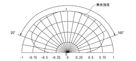
- FIG. 4 shows the measurement results of the light distribution of the white light source obtained in Comparative Example 2.
- the white light source obtained in Example 1 shown in FIG. 3 emits light in the range of 20 ° to 160 ° as compared with the white light source obtained in Comparative Example 2 shown in FIG. It was found that the strength was uniform and variation was small.
- Example 6 A white light source was produced in the same manner as in Example 1 except that the type of phosphor was changed. Specifically, (Sr 0.01 Ca 0.99 ) SiAlN 3 : Eu as a red phosphor, and (Sr 1.58 Ba 0.11 Mg 0.2 Eu 0.1 Mn 0.01 ) as a green phosphor. SiO 4, as a blue phosphor (Sr 0.85 Ba 0.01 Ca 0.09 Eu 0.05) 10 (PO 4) was used 3 Cl. The emitted light from the obtained white light source had a luminous flux of 37 lm, x in the CIE XYZ color system was 0.29, and y was 0.23.
Landscapes
- Chemical & Material Sciences (AREA)
- Inorganic Chemistry (AREA)
- Engineering & Computer Science (AREA)
- Materials Engineering (AREA)
- Organic Chemistry (AREA)
- Led Device Packages (AREA)
Abstract
Description
[数1]
L=1/(n・σ) (1)
(n:蛍光体層の単位体積当たりの蛍光体個数(pcs/mm3)、σ:蛍光体層中の蛍光体の平均クロスセクション面積(mm2))
前記tとLとが3.2≦t/Lを満たすことを特徴とする。
2 絶縁性基板
3 LEDチップ
4 蛍光体層
41 蛍光体層の第1形状部
42 蛍光体層の第2形状部
43 ドーム状の端面
以下、本発明に係る白色光源について説明する。図1は本発明の白色光源の一例を示す断面図である。図中、1は白色光源、2は絶縁性基板、3はLEDチップ、4は蛍光体層、xは蛍光体層の高さ、yは蛍光体層の胴体部の高さである。
絶縁性基板2は、電気絶縁性を有する基板である。絶縁性基板2としては、たとえばセラミックス基板やプリント基板が挙げられる。絶縁性基板2は、必要な個所にLEDチップ3と導通するための配線が設けられている。
絶縁性基板2上にはLEDチップ3が配置される。
蛍光体層4は、発光ダイオードチップ3を覆うように形成され、蛍光体として赤色発光蛍光体、緑色発光蛍光体および青色発光蛍光体を含有し、蛍光体が透明樹脂硬化物中に分散してなるものである。
赤色蛍光体粉末としては、励起波長330nm~410nmの光によりピーク波長620nm以上780nm以下の赤色光を発光する赤色蛍光体粉末が用いられる。赤色蛍光体粉末としては、たとえば、下記式(2)で表される組成のユーロピウム付活酸硫化ランタンからなる赤色蛍光体粉末、および下記式(3)で表される組成を有する赤色蛍光体粉末の少なくとも1種からなる粉末が用いられる。
(La1-x-yEuxMy)2O2S (2)
(式中、Mは、Sb、Sm、GaおよびSnから選ばれる少なくとも1種の元素であり、xおよびyは、0.01<x<0.15、0≦y<0.03を満たす値である。)
式(2)中のMがSb、Sm、GaおよびSnから選ばれる少なくとも1種の元素であると、赤色蛍光体粉末の発光効率が高いため好ましい。
(SrxCa1-x)SiAlN3:Eu (3)
(式中、xは0≦x<0.4を満たす値である。)
式(3)中のxが上記範囲内にあると、赤色蛍光体粉末が発光する光の波長域が適切になるとともに、発光効率が高く、波長域と発光効率とのバランスがよいため好ましい。式(3)中のxが上記範囲内で大きくなるほど赤色蛍光体粉末が発光する光が短波長化しやすく、上記範囲内で小さくなるほど赤色蛍光体粉末の発光効率が高くなりやすい。
緑色蛍光体粉末としては、励起波長330nm~410nmの光によりピーク波長490nm~575nmの緑色光を発光する緑色蛍光体粉末が用いられる。緑色蛍光体粉末としては、たとえば、下記式(4)で表される組成のユーロピウムマンガン付活アルミン酸塩および下記式(5)で表される組成を有する緑色蛍光体粉末の少なくとも1種からなる粉末が用いられる。
(Ba1-x-y-zSrxCayEuz)(Mg1-uMnu)Al10O17 (4)
(式中、x、y、zおよびuは、0≦x<0.2、0≦y<0.1、0.005<z<0.5、0.1<u<0.5を満たす値である。)
式(4)中のzおよびuがそれぞれ上記範囲内にあると、緑色蛍光体粉末の発光効率が高いため好ましい。式(4)中のxおよびyがそれぞれ上記範囲内にあると、緑色蛍光体粉末の寿命と輝度のバランスがよいため好ましい。式(4)中のxが0.2以上であると緑色蛍光体粉末の寿命が低下するおそれがある。
(Sr2-x-y-z-uBaxMgyEuzMnu)SiO4 (5)
(式中、x、y、zおよびuは、0.1<x<0.4、0.005<y<0.21、0.05<z<0.3、0.001<u<0.04を満たす値である。)
式(5)中のxが上記範囲内にあると、緑色蛍光体粉末が発光する光の波長が照明用およびバックライト用に適するため好ましい。また、式(5)中のxが上記範囲内で大きくなるほど、緑色蛍光体粉末が発光する光の波長が短波長化しバックライト用により適するようになる。
青色蛍光体粉末としては、励起波長330nm~410nmの光によりピーク波長430nm~460nmの青色光を発光する青色蛍光体粉末が用いられる。青色蛍光体粉末としては、たとえば、下記式(6)で表される組成を有する青色蛍光体粉末が用いられる。
(Sr1-x-y-zBaxCayEuz)5(PO4)3Cl (6)
(式中、x、yおよびzは、0≦x<0.5、0≦y<0.1、0.005<z<0.1を満たす値である。)
式(6)中のxおよびyがそれぞれ上記範囲内にあると、青色蛍光体粉末が発光する光の波長が照明用途やバックライト用途の白色LEDランプに適するため好ましい。
[数2]
L=1/(n・σ) (1)
(n: 蛍光体層の単位体積当たりの蛍光体個数(pcs/mm3)、σ:蛍光体層中の蛍光体の平均クロスセクション面積(mm2))
前記tとLとが3.2≦t/Lを満たす。
はじめに、蛍光体と透明樹脂とを含むペースト原料を調製する。ペースト原料は、蛍光体と透明樹脂とを、公知の撹拌機等を用いて混合することにより得られる。ペースト原料は、蛍光体含有率が高くかつ比較的高粘度になるように調製することが好ましい。
次に、ペースト原料を分散処理することにより、蛍光体が透明樹脂中に充分に分散した蛍光体ペースト組成物を調製する。蛍光体ペースト組成物は、混合分散装置を用いてペースト原料を分散処理することにより得られる。
次に、LEDチップを実装した絶縁性基板を用意し、この絶縁性基板上のLEDチップを覆うように蛍光体ペースト組成物を塗布し、乾燥させて、絶縁性基板上に蛍光体層を形成する。
本発明に係るバックライトは、本発明に係る白色光源を用いたものである。本発明に係るバックライトは、上記白色光源を用い、公知の方法で作製することができる。
本発明に係る液晶表示装置は、本発明に係るバックライトを具備したものである。本発明に係る液晶表示装置は、上記バックライトを用い、公知の方法で作製することができる。
本発明に係る照明装置は、本発明に係る白色光源を用いたものである。本発明に係る照明装置は、上記白色光源を用い、公知の方法で作製することができる。
(発光ダイオードチップの実装)
縦3mm×横3mm×厚さ0.2mmの窒化アルミニウム絶縁性基板(熱伝導率220W/m・K)を用い、その表面に順にTi/Pt/Auの各層からなる正方形状の金属パターンを複数個形成した。また、窒化アルミニウム絶縁性基板はスルーホールにより裏面側に導通する構造とし、基板の裏面には電極パッドを形成した。
以下の手順により、発光ダイオードチップが搭載された絶縁性基板上に蛍光体層を形成した。
はじめに、青色蛍光体、緑色蛍光体および赤色蛍光体と、シリコーン樹脂とを混合撹拌機を用いて混合し、ペースト原料を調製した。
次に、ハイアルミナロールを備えた3本ロールミルを用い、ペースト原料を8時間分散処理した(第1分散処理)。第1分散処理後、脱泡攪拌機を用い、ペースト原料を5mTorrで10分間脱泡処理した(第1脱泡処理)。第1脱泡処理後、ペースト原料を第1分散処理と同条件で分散処理した(第2分散処理)。第2分散処理後、ペースト原料を第1脱泡処理と同条件で脱泡処理した(第2脱泡処理)。第2脱泡処理後、ペースト原料を第1分散処理と同条件で分散処理した(第3分散処理)。第3分散処理後、蛍光体ペースト組成物が得られた。蛍光体ペースト組成物は、粘度が6000Pa・sであった。
発光ダイオードチップが搭載された絶縁性基板を用意し、この絶縁性基板上の発光ダイオードチップを覆うように蛍光体ペースト組成物を塗布し、乾燥させて、絶縁性基板上に蛍光体層を形成した。蛍光体層は、図1に示すような砲弾型に形成した。蛍光体層の形成により白色光源が得られた。
得られた白色光源について配光性の測定を行った。光度の測定はJIS-C-8152コンディションBにより測定した。また、配光性ばらつきは20°~160°の範囲において、配光性ばらつき=(光度最低値/光度最高値)の式により算出した。

白色光源の製造条件を表1および表2に示すように変えた以外は、実施例1と同様にして白色光源を作製した。
蛍光体の種類を変えた以外は実施例1と同様にして、白色光源を作製した。具体的には、赤色蛍光体として(Sr0.01Ca0.99)SiAlN3:Eu、緑色蛍光体として(Sr1.58Ba0.11Mg0.2Eu0.1Mn0.01)SiO4、青色蛍光体として(Sr0.85Ba0.01Ca0.09Eu0.05)10(PO4)3Clを用いた。得られた白色光源からの出射光は光束が37lm、CIEのXYZ表色系でのxが0.29、yが0.23であった。
Claims (10)
- 絶縁性基板と、
前記絶縁性基板上に配置され、波長330nm~410nmの紫外光を発生する発光ダイオードチップと、
前記発光ダイオードチップを覆うように形成され、蛍光体として赤色発光蛍光体、緑色発光蛍光体および青色発光蛍光体を含有し前記蛍光体が透明樹脂硬化物中に分散してなる蛍光体層と、
を具備する白色光源において、
前記蛍光体層の表面と前記発光ダイオードチップの外周部との最短距離をt(mm)、下記式(1)で定義される平均自由工程をL(mm)としたとき、
[数1]
L=1/(n・σ) (1)
(n:蛍光体層の単位体積当たりの蛍光体個数(pcs/mm3)、σ:蛍光体層中の蛍光体の平均クロスセクション面積(mm2))
前記tとLとが3.2≦t/Lを満たすことを特徴とする白色光源。 - 前記蛍光体層は、
前記絶縁性基板側に形成された円柱状の第1形状部と、
この第1形状部の端部に連続して形成されたドーム状の第2形状部と、
からなり、ドーム状の端面を有する筒状体であり、
前記第1形状部の軸方向の長さは、前記蛍光体層全体の軸方向の長さに対して10%以上であることを特徴とする請求項1の白色光源。 - 前記tとLとが3.2≦t/L≦6を満たすことを特徴とする請求項1または2に記載の白色光源。
- 前記赤色発光蛍光体は、
下記式(2)で表わされる組成の蛍光体粉末;
[化1]
(La1-x-yEuxMy)2O2S (2)
(式中、MはSb、Sm、GaおよびSnから選ばれる少なくとも1種の元素であり、xおよびyは0.01<x<0.15、0≦y<0.03を満たす値である。)
および下記式(3)で表わされる組成の蛍光体粉末;
[化2]
(SrxCa1-x)SiAiN3:Eu (3)
(式中、xは0≦x<0.4を満たす値である。)
の少なくとも1種からなることを特徴とする請求項1乃至3のいずれか1項に記載の白色光源。 - 前記緑色発光蛍光体は、
下記式(4)で表わされる組成の蛍光体粉末;
[化3]
(Ba1-x-y-zSrxCayEuz)(Mg1-uMnu)Al10O17 (4)
(式中、x、y、z、およびuは、0≦x<0.2、0≦y<0.1、0.005<z<0.5、0.1<u<0.5を満たす値である。)
および下記式(5)で表わされる組成の蛍光体粉末;
[化4]
(Sr2-x-y-z-uBaxMgyEuzMnu)SiO4 (5)
(式中、x、y、z、およびuは、0.1<x<0.4、0.005<y<0.21、0.05<z<0.3、0.001<u<0.04を満たす値である。)
の少なくとも1種からなることを特徴とする請求項1乃至3のいずれか1項に記載の白色光源。 - 前記青色発光蛍光体は、下記式(6)で表わされる組成の蛍光体粉末
[化5]
(Sr1-x-y―zBaxCayEuz)5(PO4)3Cl (6)
(式中、x、yおよびzは、0≦x<0.5、0≦y<0.1、0.005<z<0.1を満たす値である。)
からなることを特徴とする請求項1乃至3のいずれか1項に記載の白色光源。 - 前記蛍光体の平均粒径が10μm~60μmであることを特徴とする請求項1乃至6
のいずれか1項に記載の白色光源。 - 請求項1乃至7のいずれか1項に記載の白色光源を用いたことを特徴とするバックライト。
- 請求項8記載のバックライトを具備したことを特徴とする液晶表示装置。
- 請求項1乃至7のいずれか1項に記載の白色光源を用いたことを特徴とする照明装置。
Priority Applications (2)
| Application Number | Priority Date | Filing Date | Title |
|---|---|---|---|
| US12/995,352 US8344407B2 (en) | 2008-05-30 | 2009-05-28 | White light source, backlight, liquid crystal display apparatus, and illuminating apparatus |
| JP2010514534A JP5524051B2 (ja) | 2008-05-30 | 2009-05-28 | 白色光源、バックライト、液晶表示装置および照明装置 |
Applications Claiming Priority (2)
| Application Number | Priority Date | Filing Date | Title |
|---|---|---|---|
| JP2008142295 | 2008-05-30 | ||
| JP2008-142295 | 2008-05-30 |
Publications (1)
| Publication Number | Publication Date |
|---|---|
| WO2009145259A1 true WO2009145259A1 (ja) | 2009-12-03 |
Family
ID=41377129
Family Applications (1)
| Application Number | Title | Priority Date | Filing Date |
|---|---|---|---|
| PCT/JP2009/059780 Ceased WO2009145259A1 (ja) | 2008-05-30 | 2009-05-28 | 白色光源、バックライト、液晶表示装置および照明装置 |
Country Status (3)
| Country | Link |
|---|---|
| US (1) | US8344407B2 (ja) |
| JP (1) | JP5524051B2 (ja) |
| WO (1) | WO2009145259A1 (ja) |
Cited By (8)
| Publication number | Priority date | Publication date | Assignee | Title |
|---|---|---|---|---|
| JP2010278246A (ja) * | 2009-05-28 | 2010-12-09 | Toshiba Lighting & Technology Corp | 発光モジュール及びその製造方法 |
| KR20110102063A (ko) * | 2010-03-10 | 2011-09-16 | 삼성엘이디 주식회사 | 광효율이 개선된 led 장치 |
| JP2011187660A (ja) * | 2010-03-08 | 2011-09-22 | Hiroshi Ninomiya | ベアチップ実装面発光体及びその製造方法 |
| WO2012001927A1 (ja) * | 2010-06-28 | 2012-01-05 | 株式会社 東芝 | Led電球 |
| WO2012035762A1 (ja) * | 2010-09-16 | 2012-03-22 | 株式会社 東芝 | 発光装置とled電球 |
| WO2013118571A1 (ja) * | 2012-02-06 | 2013-08-15 | 株式会社小糸製作所 | 半導体発光装置 |
| JP5732059B2 (ja) * | 2010-08-31 | 2015-06-10 | 株式会社東芝 | Led電球 |
| US10619094B2 (en) | 2017-08-31 | 2020-04-14 | Nichia Corporation | Aluminate fluorescent material and light emitting device |
Families Citing this family (5)
| Publication number | Priority date | Publication date | Assignee | Title |
|---|---|---|---|---|
| DE102010028246A1 (de) * | 2010-04-27 | 2011-10-27 | Osram Opto Semiconductors Gmbh | Optoelektronisches Bauelement und Verfahren zum Herstellen eines optoelektronischen Bauelements |
| JP5899507B2 (ja) * | 2011-04-27 | 2016-04-06 | パナソニックIpマネジメント株式会社 | 発光装置及びそれを用いた照明装置 |
| JP5899508B2 (ja) * | 2011-04-28 | 2016-04-06 | パナソニックIpマネジメント株式会社 | 発光装置及びそれを用いた照明装置 |
| CN103733362B (zh) * | 2011-08-16 | 2017-03-29 | 三星电子株式会社 | 具有改善的发光效力的led器件 |
| CN103557454A (zh) * | 2013-10-29 | 2014-02-05 | 南京琦光光电科技有限公司 | 一种360°发光的白光led三维光源模组 |
Citations (4)
| Publication number | Priority date | Publication date | Assignee | Title |
|---|---|---|---|---|
| JPH11298047A (ja) * | 1998-04-13 | 1999-10-29 | Nichia Chem Ind Ltd | 発光装置 |
| JP2004071726A (ja) * | 2002-08-05 | 2004-03-04 | Nichia Chem Ind Ltd | 発光装置 |
| JP2006324418A (ja) * | 2005-05-18 | 2006-11-30 | Mitsubishi Chemicals Corp | 発光装置 |
| JP2008077104A (ja) * | 2007-11-12 | 2008-04-03 | Rabo Sufia Kk | バルク型レンズ、発光体、受光体、照明器具及びバルク型レンズの製造方法 |
Family Cites Families (2)
| Publication number | Priority date | Publication date | Assignee | Title |
|---|---|---|---|---|
| WO2003080764A1 (en) * | 2002-03-22 | 2003-10-02 | Nichia Corporation | Nitride phosphor and method for preparation thereof, and light emitting device |
| JP5235266B2 (ja) * | 2005-09-29 | 2013-07-10 | 株式会社東芝 | 白色ledの製造方法およびそれを用いたバックライトの製造方法並びに液晶表示装置の製造方法 |
-
2009
- 2009-05-28 US US12/995,352 patent/US8344407B2/en active Active
- 2009-05-28 WO PCT/JP2009/059780 patent/WO2009145259A1/ja not_active Ceased
- 2009-05-28 JP JP2010514534A patent/JP5524051B2/ja active Active
Patent Citations (4)
| Publication number | Priority date | Publication date | Assignee | Title |
|---|---|---|---|---|
| JPH11298047A (ja) * | 1998-04-13 | 1999-10-29 | Nichia Chem Ind Ltd | 発光装置 |
| JP2004071726A (ja) * | 2002-08-05 | 2004-03-04 | Nichia Chem Ind Ltd | 発光装置 |
| JP2006324418A (ja) * | 2005-05-18 | 2006-11-30 | Mitsubishi Chemicals Corp | 発光装置 |
| JP2008077104A (ja) * | 2007-11-12 | 2008-04-03 | Rabo Sufia Kk | バルク型レンズ、発光体、受光体、照明器具及びバルク型レンズの製造方法 |
Cited By (16)
| Publication number | Priority date | Publication date | Assignee | Title |
|---|---|---|---|---|
| JP2010278246A (ja) * | 2009-05-28 | 2010-12-09 | Toshiba Lighting & Technology Corp | 発光モジュール及びその製造方法 |
| JP2011187660A (ja) * | 2010-03-08 | 2011-09-22 | Hiroshi Ninomiya | ベアチップ実装面発光体及びその製造方法 |
| KR20110102063A (ko) * | 2010-03-10 | 2011-09-16 | 삼성엘이디 주식회사 | 광효율이 개선된 led 장치 |
| KR101625911B1 (ko) * | 2010-03-10 | 2016-06-01 | 삼성전자주식회사 | 광효율이 개선된 led 장치 |
| US8955996B2 (en) | 2010-06-28 | 2015-02-17 | Kabushiki Kaisha Toshiba | LED light bulb |
| WO2012001927A1 (ja) * | 2010-06-28 | 2012-01-05 | 株式会社 東芝 | Led電球 |
| JP5732059B2 (ja) * | 2010-08-31 | 2015-06-10 | 株式会社東芝 | Led電球 |
| WO2012035762A1 (ja) * | 2010-09-16 | 2012-03-22 | 株式会社 東芝 | 発光装置とled電球 |
| JPWO2012035762A1 (ja) * | 2010-09-16 | 2014-01-20 | 株式会社東芝 | 発光装置とled電球 |
| CN102959743B (zh) * | 2010-09-16 | 2015-06-17 | 株式会社东芝 | 发光装置和led灯泡 |
| CN102959743A (zh) * | 2010-09-16 | 2013-03-06 | 株式会社东芝 | 发光装置和led灯泡 |
| JP2013161967A (ja) * | 2012-02-06 | 2013-08-19 | Koito Mfg Co Ltd | 半導体発光装置 |
| WO2013118571A1 (ja) * | 2012-02-06 | 2013-08-15 | 株式会社小糸製作所 | 半導体発光装置 |
| US9406657B2 (en) | 2012-02-06 | 2016-08-02 | Koito Manufacturing Co., Ltd. | Semiconductor light-emitting device |
| US10619094B2 (en) | 2017-08-31 | 2020-04-14 | Nichia Corporation | Aluminate fluorescent material and light emitting device |
| US10829688B2 (en) | 2017-08-31 | 2020-11-10 | Nichia Corporation | Aluminate fluorescent material and light emitting device |
Also Published As
| Publication number | Publication date |
|---|---|
| US20110073899A1 (en) | 2011-03-31 |
| JPWO2009145259A1 (ja) | 2011-10-13 |
| JP5524051B2 (ja) | 2014-06-18 |
| US8344407B2 (en) | 2013-01-01 |
Similar Documents
| Publication | Publication Date | Title |
|---|---|---|
| JP5524051B2 (ja) | 白色光源、バックライト、液晶表示装置および照明装置 | |
| JP5747023B2 (ja) | 白色発光ランプおよびそれを用いた白色led照明装置 | |
| US10008644B2 (en) | Light emitting device and fabricating method thereof | |
| JP5777520B2 (ja) | 白色発光ランプおよびそれを用いた白色led照明装置 | |
| JP4767243B2 (ja) | 白色光源、バックライトユニットおよびlcdディスプレイ | |
| JP7312187B2 (ja) | 蛍光体及び発光装置 | |
| JP6165248B2 (ja) | 発光装置 | |
| JP5127455B2 (ja) | 白色発光装置とその製造方法、およびそれを用いたバックライト並びに液晶表示装置 | |
| JPWO2008096545A1 (ja) | 白色発光ランプとそれを用いた照明装置 | |
| JP2013038447A (ja) | 白色ledランプ、バックライトおよび照明装置 | |
| CN104837954A (zh) | 荧光体、发光元件及照明装置 | |
| TW201207086A (en) | β -SiAlON, method for producing β -SiAlON, and light-emitting device | |
| JP2011151419A (ja) | 発光装置とその製造方法 | |
| JP6546583B2 (ja) | 疎水化処理蛍光体及び発光装置 | |
| JP5398141B2 (ja) | 白色発光型ledランプおよびそれを用いたバックライト並びに液晶表示装置 | |
| JP5635268B2 (ja) | 白色発光装置及びこれを用いた車両用灯具 | |
| JP6405738B2 (ja) | 発光装置 | |
| JP2012195420A (ja) | 白色発光装置 | |
| CN118647689A (zh) | 荧光体粉末、含荧光体组合物、发光元件和发光装置 | |
| TWI463690B (zh) | A semiconductor light emitting device, and a semiconductor light emitting device | |
| JP2025088371A (ja) | 波長変換部材、および発光装置 | |
| TW202440872A (zh) | 螢光體片材、發光元件及發光裝置 | |
| JP2015015435A (ja) | 発光体及びこれを備える発光装置 |
Legal Events
| Date | Code | Title | Description |
|---|---|---|---|
| 121 | Ep: the epo has been informed by wipo that ep was designated in this application |
Ref document number: 09754767 Country of ref document: EP Kind code of ref document: A1 |
|
| WWE | Wipo information: entry into national phase |
Ref document number: 2010514534 Country of ref document: JP |
|
| WWE | Wipo information: entry into national phase |
Ref document number: 12995352 Country of ref document: US |
|
| NENP | Non-entry into the national phase |
Ref country code: DE |
|
| 122 | Ep: pct application non-entry in european phase |
Ref document number: 09754767 Country of ref document: EP Kind code of ref document: A1 |