WO2009145131A1 - 化合物半導体発光素子およびそれを用いる照明装置ならびに化合物半導体発光素子の製造方法 - Google Patents
化合物半導体発光素子およびそれを用いる照明装置ならびに化合物半導体発光素子の製造方法 Download PDFInfo
- Publication number
- WO2009145131A1 WO2009145131A1 PCT/JP2009/059504 JP2009059504W WO2009145131A1 WO 2009145131 A1 WO2009145131 A1 WO 2009145131A1 JP 2009059504 W JP2009059504 W JP 2009059504W WO 2009145131 A1 WO2009145131 A1 WO 2009145131A1
- Authority
- WO
- WIPO (PCT)
- Prior art keywords
- region
- columnar crystal
- substrate
- light emitting
- layer
- Prior art date
Links
- 239000004065 semiconductor Substances 0.000 title claims abstract description 84
- 150000001875 compounds Chemical class 0.000 title claims abstract description 40
- 238000000034 method Methods 0.000 title claims description 31
- 238000004519 manufacturing process Methods 0.000 title claims description 13
- 239000000758 substrate Substances 0.000 claims abstract description 62
- 239000013078 crystal Substances 0.000 claims description 96
- 238000001228 spectrum Methods 0.000 claims description 8
- 238000010586 diagram Methods 0.000 claims description 7
- 238000005286 illumination Methods 0.000 claims description 5
- 238000005304 joining Methods 0.000 claims description 2
- OAICVXFJPJFONN-UHFFFAOYSA-N Phosphorus Chemical compound [P] OAICVXFJPJFONN-UHFFFAOYSA-N 0.000 description 19
- 125000004429 atom Chemical group 0.000 description 12
- 230000004907 flux Effects 0.000 description 9
- 239000000463 material Substances 0.000 description 6
- 238000009792 diffusion process Methods 0.000 description 5
- QGZKDVFQNNGYKY-UHFFFAOYSA-N Ammonia Chemical compound N QGZKDVFQNNGYKY-UHFFFAOYSA-N 0.000 description 4
- 230000005284 excitation Effects 0.000 description 4
- 238000009877 rendering Methods 0.000 description 4
- 238000001505 atmospheric-pressure chemical vapour deposition Methods 0.000 description 3
- 239000012535 impurity Substances 0.000 description 3
- 239000011777 magnesium Substances 0.000 description 3
- 238000001451 molecular beam epitaxy Methods 0.000 description 3
- 239000002073 nanorod Substances 0.000 description 3
- 150000004767 nitrides Chemical class 0.000 description 3
- IJGRMHOSHXDMSA-UHFFFAOYSA-N Atomic nitrogen Chemical compound N#N IJGRMHOSHXDMSA-UHFFFAOYSA-N 0.000 description 2
- BLRPTPMANUNPDV-UHFFFAOYSA-N Silane Chemical compound [SiH4] BLRPTPMANUNPDV-UHFFFAOYSA-N 0.000 description 2
- 229910021529 ammonia Inorganic materials 0.000 description 2
- 239000012159 carrier gas Substances 0.000 description 2
- 230000007547 defect Effects 0.000 description 2
- 239000007789 gas Substances 0.000 description 2
- 238000001459 lithography Methods 0.000 description 2
- 239000002994 raw material Substances 0.000 description 2
- 230000006798 recombination Effects 0.000 description 2
- 238000005215 recombination Methods 0.000 description 2
- 229910000077 silane Inorganic materials 0.000 description 2
- 239000007787 solid Substances 0.000 description 2
- 238000001179 sorption measurement Methods 0.000 description 2
- 238000002336 sorption--desorption measurement Methods 0.000 description 2
- IBEFSUTVZWZJEL-UHFFFAOYSA-N trimethylindium Chemical compound C[In](C)C IBEFSUTVZWZJEL-UHFFFAOYSA-N 0.000 description 2
- 238000007740 vapor deposition Methods 0.000 description 2
- MHYQBXJRURFKIN-UHFFFAOYSA-N C1(C=CC=C1)[Mg] Chemical compound C1(C=CC=C1)[Mg] MHYQBXJRURFKIN-UHFFFAOYSA-N 0.000 description 1
- UFHFLCQGNIYNRP-UHFFFAOYSA-N Hydrogen Chemical compound [H][H] UFHFLCQGNIYNRP-UHFFFAOYSA-N 0.000 description 1
- BPQQTUXANYXVAA-UHFFFAOYSA-N Orthosilicate Chemical compound [O-][Si]([O-])([O-])[O-] BPQQTUXANYXVAA-UHFFFAOYSA-N 0.000 description 1
- UCKMPCXJQFINFW-UHFFFAOYSA-N Sulphide Chemical compound [S-2] UCKMPCXJQFINFW-UHFFFAOYSA-N 0.000 description 1
- 239000000969 carrier Substances 0.000 description 1
- 238000006243 chemical reaction Methods 0.000 description 1
- 239000003086 colorant Substances 0.000 description 1
- 230000003247 decreasing effect Effects 0.000 description 1
- 238000005516 engineering process Methods 0.000 description 1
- 238000002474 experimental method Methods 0.000 description 1
- 238000006703 hydration reaction Methods 0.000 description 1
- 229910052757 nitrogen Inorganic materials 0.000 description 1
- 125000004433 nitrogen atom Chemical group N* 0.000 description 1
- 230000003287 optical effect Effects 0.000 description 1
- 230000001737 promoting effect Effects 0.000 description 1
- XCZXGTMEAKBVPV-UHFFFAOYSA-N trimethylgallium Chemical compound C[Ga](C)C XCZXGTMEAKBVPV-UHFFFAOYSA-N 0.000 description 1
Images


Classifications
-
- H—ELECTRICITY
- H01—ELECTRIC ELEMENTS
- H01L—SEMICONDUCTOR DEVICES NOT COVERED BY CLASS H10
- H01L33/00—Semiconductor devices having potential barriers specially adapted for light emission; Processes or apparatus specially adapted for the manufacture or treatment thereof or of parts thereof; Details thereof
- H01L33/02—Semiconductor devices having potential barriers specially adapted for light emission; Processes or apparatus specially adapted for the manufacture or treatment thereof or of parts thereof; Details thereof characterised by the semiconductor bodies
- H01L33/20—Semiconductor devices having potential barriers specially adapted for light emission; Processes or apparatus specially adapted for the manufacture or treatment thereof or of parts thereof; Details thereof characterised by the semiconductor bodies with a particular shape, e.g. curved or truncated substrate
-
- H—ELECTRICITY
- H01—ELECTRIC ELEMENTS
- H01L—SEMICONDUCTOR DEVICES NOT COVERED BY CLASS H10
- H01L21/00—Processes or apparatus adapted for the manufacture or treatment of semiconductor or solid state devices or of parts thereof
- H01L21/02—Manufacture or treatment of semiconductor devices or of parts thereof
- H01L21/02104—Forming layers
- H01L21/02365—Forming inorganic semiconducting materials on a substrate
- H01L21/02367—Substrates
- H01L21/0237—Materials
- H01L21/02373—Group 14 semiconducting materials
- H01L21/02381—Silicon, silicon germanium, germanium
-
- H—ELECTRICITY
- H01—ELECTRIC ELEMENTS
- H01L—SEMICONDUCTOR DEVICES NOT COVERED BY CLASS H10
- H01L21/00—Processes or apparatus adapted for the manufacture or treatment of semiconductor or solid state devices or of parts thereof
- H01L21/02—Manufacture or treatment of semiconductor devices or of parts thereof
- H01L21/02104—Forming layers
- H01L21/02365—Forming inorganic semiconducting materials on a substrate
- H01L21/02436—Intermediate layers between substrates and deposited layers
- H01L21/02439—Materials
- H01L21/02455—Group 13/15 materials
- H01L21/02458—Nitrides
-
- H—ELECTRICITY
- H01—ELECTRIC ELEMENTS
- H01L—SEMICONDUCTOR DEVICES NOT COVERED BY CLASS H10
- H01L21/00—Processes or apparatus adapted for the manufacture or treatment of semiconductor or solid state devices or of parts thereof
- H01L21/02—Manufacture or treatment of semiconductor devices or of parts thereof
- H01L21/02104—Forming layers
- H01L21/02365—Forming inorganic semiconducting materials on a substrate
- H01L21/02518—Deposited layers
- H01L21/02521—Materials
- H01L21/02538—Group 13/15 materials
- H01L21/0254—Nitrides
-
- H—ELECTRICITY
- H01—ELECTRIC ELEMENTS
- H01L—SEMICONDUCTOR DEVICES NOT COVERED BY CLASS H10
- H01L21/00—Processes or apparatus adapted for the manufacture or treatment of semiconductor or solid state devices or of parts thereof
- H01L21/02—Manufacture or treatment of semiconductor devices or of parts thereof
- H01L21/02104—Forming layers
- H01L21/02365—Forming inorganic semiconducting materials on a substrate
- H01L21/02518—Deposited layers
- H01L21/0257—Doping during depositing
- H01L21/02573—Conductivity type
- H01L21/02576—N-type
-
- H—ELECTRICITY
- H01—ELECTRIC ELEMENTS
- H01L—SEMICONDUCTOR DEVICES NOT COVERED BY CLASS H10
- H01L21/00—Processes or apparatus adapted for the manufacture or treatment of semiconductor or solid state devices or of parts thereof
- H01L21/02—Manufacture or treatment of semiconductor devices or of parts thereof
- H01L21/02104—Forming layers
- H01L21/02365—Forming inorganic semiconducting materials on a substrate
- H01L21/02518—Deposited layers
- H01L21/0257—Doping during depositing
- H01L21/02573—Conductivity type
- H01L21/02579—P-type
-
- H—ELECTRICITY
- H01—ELECTRIC ELEMENTS
- H01L—SEMICONDUCTOR DEVICES NOT COVERED BY CLASS H10
- H01L21/00—Processes or apparatus adapted for the manufacture or treatment of semiconductor or solid state devices or of parts thereof
- H01L21/02—Manufacture or treatment of semiconductor devices or of parts thereof
- H01L21/02104—Forming layers
- H01L21/02365—Forming inorganic semiconducting materials on a substrate
- H01L21/02518—Deposited layers
- H01L21/02587—Structure
- H01L21/0259—Microstructure
- H01L21/02603—Nanowires
-
- H—ELECTRICITY
- H01—ELECTRIC ELEMENTS
- H01L—SEMICONDUCTOR DEVICES NOT COVERED BY CLASS H10
- H01L21/00—Processes or apparatus adapted for the manufacture or treatment of semiconductor or solid state devices or of parts thereof
- H01L21/02—Manufacture or treatment of semiconductor devices or of parts thereof
- H01L21/02104—Forming layers
- H01L21/02365—Forming inorganic semiconducting materials on a substrate
- H01L21/02612—Formation types
- H01L21/02617—Deposition types
- H01L21/0262—Reduction or decomposition of gaseous compounds, e.g. CVD
-
- H—ELECTRICITY
- H01—ELECTRIC ELEMENTS
- H01L—SEMICONDUCTOR DEVICES NOT COVERED BY CLASS H10
- H01L21/00—Processes or apparatus adapted for the manufacture or treatment of semiconductor or solid state devices or of parts thereof
- H01L21/02—Manufacture or treatment of semiconductor devices or of parts thereof
- H01L21/02104—Forming layers
- H01L21/02365—Forming inorganic semiconducting materials on a substrate
- H01L21/02612—Formation types
- H01L21/02617—Deposition types
- H01L21/02636—Selective deposition, e.g. simultaneous growth of mono- and non-monocrystalline semiconductor materials
- H01L21/02639—Preparation of substrate for selective deposition
-
- H—ELECTRICITY
- H01—ELECTRIC ELEMENTS
- H01L—SEMICONDUCTOR DEVICES NOT COVERED BY CLASS H10
- H01L21/00—Processes or apparatus adapted for the manufacture or treatment of semiconductor or solid state devices or of parts thereof
- H01L21/02—Manufacture or treatment of semiconductor devices or of parts thereof
- H01L21/02104—Forming layers
- H01L21/02365—Forming inorganic semiconducting materials on a substrate
- H01L21/02612—Formation types
- H01L21/02617—Deposition types
- H01L21/02636—Selective deposition, e.g. simultaneous growth of mono- and non-monocrystalline semiconductor materials
- H01L21/02647—Lateral overgrowth
- H01L21/0265—Pendeoepitaxy
-
- H—ELECTRICITY
- H01—ELECTRIC ELEMENTS
- H01L—SEMICONDUCTOR DEVICES NOT COVERED BY CLASS H10
- H01L33/00—Semiconductor devices having potential barriers specially adapted for light emission; Processes or apparatus specially adapted for the manufacture or treatment thereof or of parts thereof; Details thereof
- H01L33/02—Semiconductor devices having potential barriers specially adapted for light emission; Processes or apparatus specially adapted for the manufacture or treatment thereof or of parts thereof; Details thereof characterised by the semiconductor bodies
- H01L33/08—Semiconductor devices having potential barriers specially adapted for light emission; Processes or apparatus specially adapted for the manufacture or treatment thereof or of parts thereof; Details thereof characterised by the semiconductor bodies with a plurality of light emitting regions, e.g. laterally discontinuous light emitting layer or photoluminescent region integrated within the semiconductor body
-
- H—ELECTRICITY
- H01—ELECTRIC ELEMENTS
- H01L—SEMICONDUCTOR DEVICES NOT COVERED BY CLASS H10
- H01L33/00—Semiconductor devices having potential barriers specially adapted for light emission; Processes or apparatus specially adapted for the manufacture or treatment thereof or of parts thereof; Details thereof
- H01L33/02—Semiconductor devices having potential barriers specially adapted for light emission; Processes or apparatus specially adapted for the manufacture or treatment thereof or of parts thereof; Details thereof characterised by the semiconductor bodies
- H01L33/16—Semiconductor devices having potential barriers specially adapted for light emission; Processes or apparatus specially adapted for the manufacture or treatment thereof or of parts thereof; Details thereof characterised by the semiconductor bodies with a particular crystal structure or orientation, e.g. polycrystalline, amorphous or porous
- H01L33/18—Semiconductor devices having potential barriers specially adapted for light emission; Processes or apparatus specially adapted for the manufacture or treatment thereof or of parts thereof; Details thereof characterised by the semiconductor bodies with a particular crystal structure or orientation, e.g. polycrystalline, amorphous or porous within the light emitting region
Definitions
- the present invention relates to a compound semiconductor light-emitting element that emits light by combining electrons and holes in a compound semiconductor, a lighting device using the same, and a method for manufacturing the compound semiconductor light-emitting element.
- the present invention relates to a structure having a plurality of columnar crystal structures called nanorods.
- nitride nitride semiconductor
- an electric current is injected from the outside, and electrons and holes are combined in the light emitting layer to emit light.
- the development of the light emitting element to be made is remarkable.
- the phosphor is excited by a part of the light emitted from the light emitting element, and the white light obtained by mixing the light generated from the phosphor and the light from the light emitting element is used as a light source to be applied to the lighting device.
- the white light obtained by mixing the light generated from the phosphor and the light from the light emitting element is used as a light source to be applied to the lighting device.
- the first factor that lowers the efficiency is that a part of energy is lost (Stokes loss) by wavelength conversion.
- the excitation light emitted from the light emitting element and absorbed by the phosphor is wavelength-converted to light having energy lower than that of the light generated from the light emitting element, and is emitted to the outside again.
- a loss is caused by the difference in energy between the excitation light from the light emitting element and the emission light from the phosphor, and the efficiency is lowered.
- the second factor for reducing the efficiency is a decrease in efficiency due to non-radiative recombination in the phosphor (decrease in internal quantum efficiency of the phosphor).
- the crystal defects present in the phosphor function as non-radiative recombination centers. This is because some of the carriers generated in the phosphor by the excitation light do not contribute to light emission and are captured by the crystal defects, thereby reducing the light emission efficiency of the phosphor.
- the red phosphor when realizing high color rendering white light emission, the red phosphor emits light weakly at present, and the color rendering properties and the light emission efficiency are in a trade-off relationship.
- the method of exciting phosphors of three colors of RGB with an ultraviolet light emitting semiconductor a phosphor with high efficiency has not been obtained at present.
- a compound semiconductor light emitting device has been proposed. Specifically, the nuclei for crystal growth are grown on the substrate at a temperature lower than the normal growth temperature of the columnar crystal structure, and the nuclei are dispersed by raising the temperature to the normal growth temperature over time. To have. Thereafter, by growing columnar crystal structures as usual, the film thickness and composition of the light emitting layer are varied, and each columnar crystal structure is caused to emit light at different wavelengths. The growth of the columnar crystal structure is described in Patent Document 2 and the like.
- Patent Document 1 is an excellent method for realizing a solid-state light source that enables multicolor light emission on the same substrate and easily in a single growth process, and thus at low cost.
- multicolor light emission is made possible by using variation in growth, there is a problem in accuracy when adjusting to a desired color tone, such as for illumination.
- An object of the present invention is to provide a compound semiconductor light-emitting element that can easily achieve a desired color at a low cost, or to adjust the color finely and with high accuracy, a lighting device using the same, and a compound semiconductor light-emitting element It is to provide a manufacturing method.
- a compound semiconductor light emitting device includes a substrate on one electrode side, a plurality of nanoscale columnar crystal structures extending in a vertical direction on the substrate, and top portions of the plurality of columnar crystal structures. And a second region having a step between the first region and a thickness of the substrate larger than that of the first region.
- a porous first mask layer is formed on the surface of the first region on the substrate, and the plurality of columnar crystal structures are formed on the first and second regions on the substrate in the n-type semiconductor layer and the light emitting layer.
- a p-type semiconductor layer are sequentially stacked.
- the growth rate of the columnar crystal structure is faster than in the second region without the porous mask layer.
- the crystal structure and the columnar crystal structure in the second region can be aligned at the same height, and the tops thereof can be connected to each other by the other electrode.
- the columnar crystal structure in the first region is longer than the columnar crystal structure in the second region by the height of the step between the first region and the second region. Then, since the columnar crystal structures have different aspect ratios in the first region and the second region, it is possible to emit light having different wavelengths in the first region and the second region.
- the aspect ratio of the columnar crystal structure in each region can be set by adjusting the size of the step between the first region and the second region.
- region can be easily set with high precision by a well-known semiconductor process, it becomes easy to adjust the color of luminescent color finely with high precision.
- a desired color can be realized with a single chip, it is easy to realize a desired color at a lower cost than when a plurality of chips are used.
- a lighting device uses the compound semiconductor light emitting element.
- the first region and the remaining region are formed by forming a recess as a first region in a partial region on the substrate on one electrode side. Forming a step between the first region and the second region, forming a porous first mask layer at the bottom of the recess as the first region, and forming n in the first and second regions.
- the above-described compound semiconductor light emitting device can be manufactured.
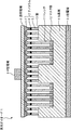
- FIG. 1 is a cross-sectional view schematically showing the structure of a light-emitting diode 1 which is a compound semiconductor light-emitting element according to an embodiment of the present invention.
- GaN is taken as an example of the material of the nanocolumn 2 (columnar crystal structure), but is not limited thereto, and all compound semiconductors including oxides, nitrides, oxynitrides, and the like are used. Can be targeted.
- MBE molecular beam epitaxy
- the light-emitting diode 1 includes a plurality of nanocolumns 2 in which an n-type semiconductor layer 5, a light-emitting layer 6, and a p-type semiconductor layer 7 are sequentially stacked on a Si substrate 4 on the n-type electrode 3 side that is one electrode. Is formed.
- a GaN nanocolumn LED is configured by connecting the top of the nanocolumn 2 with the transparent electrode 8 and the p-type electrode 9 which are the other electrodes.
- a trench 11 (first region) that is a recess is formed in a partial region on the Si substrate 4, and the nanocolumn 2 is grown in the trench 11.
- the mask layer 12 (first mask layer) to be controlled (promoted) is formed.
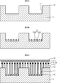
- FIG. 2 is a diagram for explaining a specific manufacturing process of the light-emitting diode 1 as described above.
- a trench 11 is formed on the n-type Si substrate 4 having a plane orientation (111) by an RIE apparatus.
- an Si oxide film is deposited on the surface of the Si substrate 4 on which the trench 11 is formed using an atmospheric pressure CVD apparatus, the outside of the trench 11, that is, the wall 13 is formed using an ordinary lithography process and an RIE apparatus.
- the upper (second region) Si oxide film is removed, and the Si oxide film is left only in the trench 11 to form the mask layer 12 shown in FIG. 2B.
- the Si oxide film 12a is inferior in density to the thermal oxide film, and thus becomes a porous film having a through hole 12b therein. Since the through-holes 12b exist at random, the thicker the Si oxide film 12a, the more rapidly the number of through-holes 12b communicating with the surface of the Si substrate 4 as shown by the mask layer 122 in FIG. 3B. Decrease. 3A and 3B viewed from the top are shown in FIGS. 3C and 3D, respectively.
- the thickness of the Si oxide film 12a is, for example, 5 nm in FIGS. 3A and 3C, and 10 nm in FIGS. 3B and 3D.
- the nanocolumn 2 is grown by the MBE apparatus as shown in FIG. 2C.
- the degree of vacuum is 2e ⁇ 5 torr
- the substrate temperature is 750 ° C.
- the plasma output is 450 W
- trimethylgallium (Ga (CH 3 ) 3 ) as a Ga source Ammonia (NH 3 ) is supplied to the nitrogen raw material.
- silane (SiH 4 ) is supplied in order to add Si having n-type conductivity as an impurity.
- the n-type semiconductor layer 5 is formed in the trench 11.
- the height of the n-type semiconductor layer 5 in the trench 11 and the n-type semiconductor layer 5 on the wall 13 becomes substantially the same.
- the n-type semiconductor layer 5 of the nanocolumn 2 grows faster in the trench 11 than on the wall 13 for the following reason. That is, since the nucleus for growing the nanocolumn 2 does not grow on the Si oxide film 12a, for example, in the case of growing the GaN nanocolumn, Ga atoms and N atoms adsorbed on the Si oxide film 12a move on the Si oxide film 12a. It is considered that it diffuses and reaches the GaN crystal nucleus in the through hole 12b and contributes to the growth of the GaN nanocolumn. As a result, compared to the thin mask 121 shown in FIG. 3A, the thick mask 122 shown in FIG.
- the 3B is supplied with a larger number of atoms contributing to the growth by the GaN crystal nuclei in the through holes 12b, and the growth rate of the nanocolumn 2 is Become faster. Therefore, in the trench 11 having the mask 12 and having the mask 12 and having a low density of crystal nuclei on the wall 13 where the nanocolumn 2 is naturally grown without the mask 12, atoms in the trench 11 contribute to the growth of crystal nuclei. As described above, the growth rate of the nanocolumn 2 becomes faster. It should be noted that changing the materials of the substrate 4 and the mask layer 12 changes the adsorption probability and diffusion rate of each atom, so that the growth rate can also be changed.
- the substrate temperature is lowered to 650 ° C.
- the impurity gas is changed from the silane (SiH 4 ) to trimethylindium (In (CH 3 ) 3 ) as an In raw material, and the flow rate of the In flux is set to 10 nm / min.
- the light emitting layer 6 made of an InGaN quantum well is grown. The growth time is 1 minute.
- the flow rate of Ga flux and the plasma output are the same as when the n-type semiconductor layer 5 is grown. What is important here is that the rate of In flux is much higher than that of Ga flux, and the rate of Ga flux is lower than the rate of N flux.
- the light emitting layer 6 may be formed in an InGaN / GaN multiple quantum well structure.
- a reflective film may be appropriately formed in the n-type semiconductor layer 5.
- the substrate temperature is raised to 750 ° C.
- the impurity gas the trimethyl indium (In (CH 3) 3) cyclopentadienyl magnesium containing Mg having p-type conductivity from (Mg (C 5 H 5) 2)
- the p-type semiconductor layer 7 is grown by changing the flow rate of Mg flux to 1 nm / min and the flow rate of Ga flux to 5 nm / min.
- the growth time is 4 minutes, and the plasma power is the same at 450 W throughout the growth of the nanocolumn 2.
- the diameter of the nanocolumn 2 is gradually increased by gradually changing the flow rate of ammonia (NH 3 ), the flow rate of the carrier gas H 2 , or the growth temperature.
- the p-type layer 14 is formed.
- a laminated p-type contact layer in which a Ni layer having a thickness of 3 nm and an ITO layer having a thickness of 10 nm are laminated on the surface of the p-type layer 14 as shown in FIG. Is formed as the transparent electrode 8, and a p-type pad electrode made of Au having a thickness of 500 nm is formed thereon as the p-type electrode 9.
- the rear surface of the Si substrate 4 is composed of a laminated n-type contact layer and an n-type pad electrode in which a 30 nm thick Ti layer and a 500 nm thick Au layer are laminated by vapor deposition with an EB vapor deposition apparatus.
- the n-type electrode 3 is formed, and the light emitting diode 1 is completed.
- a trench 11 is formed in a partial region of the Si substrate 4, a porous mask layer 12 for controlling (promoting) the growth of the nanocolumn 2 is further formed in the trench 11, and then the nanocolumn 2 is grown.
- the growth of the nanocolumn 2 is faster in the region where the mask layer 12 is present than in the region on the wall 13 where the mask layer 12 is not present. Therefore, when the nanocolumn 2 is grown for a predetermined time, the step between the trench 11 and the wall 13 is absorbed, and the surface of the p-type layer 14 becomes substantially the same height.
- at least two types of nanocolumns 2 having different heights, that is, different aspect ratios and different wavelengths indicating the maximum intensity of the spectrum of emitted light can be formed.
- FIG. 5 shows the experiment results of the present inventors.
- FIG. 5 is a graph showing the relationship between the height (length) of the nanocolumn 2 and the peak wavelength when a 300 nm diameter nanocolumn 2 is grown with the above composition. It is understood that the peak wavelength is longer as the height (length) of the nanocolumn 2 is higher (longer), that is, as the aspect ratio is larger. The reason why the peak wavelength increases as the aspect ratio increases as described above is as follows. First, the supply of atoms related to the mechanism of GaN nanocolumn growth is determined by the adsorption desorption process and the surface diffusion process. In the following, the mechanism of nanocolumn growth will be described using a rough approximation.
- the surface diffusion process is considered to be dominant for Ga atoms under the conditions of nanocolumn growth. That is, Ga atoms leave with a certain probability while diffusing from the base of the nanocolumn toward the tip. It can be assumed that the probability of leaving is proportional to the diffusion time.
- the number of Ga atoms is proportional to the diameter of the nanocolumn.
- the In / Ga ratio increases in proportion to the diameter. From the above, the In / Ga ratio that determines the wavelength depends on the aspect ratio (height / diameter) of the nanocolumn, and changes to the longer wavelength side as the aspect ratio increases.
- LED chips having different wavelengths can be formed on the same chip under the same growth conditions in a region where the mask layer 12 is present and a region on the wall 13 where the mask layer 12 is absent. . Then, the length of each nanocolumn 2 is set so as to radiate the light on the long wavelength side and the light on the short wavelength side of the straight line intersecting the white region in the CIE (Commission International de l'Eclairage) chromaticity diagram. By setting it, white light can be created.
- CIE Commission International de l'Eclairage
- the step is made into three steps, and the wavelength indicating the maximum intensity of the spectrum of the light emitted from the nanocolumn 2 in each region is light having a wavelength at the apex of the triangle surrounding the white region in the CIE chromaticity diagram.
- the mask layer 12 can be easily formed by using the Si oxide film 12a.
- the Si oxide film 12a has a through hole 12b on the order of nm, and the nanocolumn 2 is grown on the mask layer 12. Therefore, it is suitable as the mask layer 12.
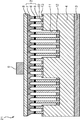
- FIG. 6 is a cross-sectional view schematically showing the structure of a light-emitting diode 21 which is a compound semiconductor light-emitting element according to another embodiment of the present invention
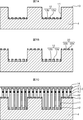
- FIG. 7 explains a specific manufacturing process of the light-emitting diode 21.
- the light-emitting diode 21 is similar to the light-emitting diode 1 described above, and corresponding portions are denoted by the same reference numerals and description thereof is omitted.
- the mask layer 22 is also formed on the wall 13 in the light emitting diode 21.
- the mask layer 22 is formed thin, and the thickness of the mask layer 22 depends on the number of the through holes 22b and the through holes 12b. It should just be chosen so that. In the case of using different materials, the adsorption probability and the diffusion rate change as described above. Therefore, the thickness may be selected so that a desired growth rate is taken into consideration.
- a 5 nm Si oxide film is deposited on the entire surface using the atmospheric pressure CVD apparatus. Thereafter, using a normal lithography process and an RIE apparatus, as shown in FIG. 7A, the Si oxide film outside the trench 11, that is, on the wall 13, is removed, and the Si oxide film 12a is left only in the trench 11. Next, using the atmospheric pressure CVD apparatus again, when a 5 nm Si oxide film is deposited on the entire surface, as shown in FIG. 7B, the 10 nm Si oxide film 12a is formed in the trench 11 and the wall 13 is formed. The 5 nm Si oxide film 22a is formed.
- the mask layer 22 with many through holes 22b is formed on the wall 13, and the mask layer 12 with few through holes 12b is formed in the trench 11, so that the growth rate of the nanocolumns 2 can be made different as described above. it can.
- a compound semiconductor light emitting device includes a substrate on one electrode side, a plurality of nanoscale columnar crystal structures extending vertically on the substrate, and the plurality of columnar crystal structures. And a second region having a step between the first region and the substrate having a thickness greater than that of the first region. And a porous first mask layer is formed on the surface of the first region on the substrate, and the plurality of columnar crystal structures are formed on the first and second regions on the substrate with an n-type semiconductor layer. A light emitting layer and a p-type semiconductor layer are sequentially laminated.
- the growth rate of the columnar crystal structure is faster than in the second region without the porous mask layer.
- the crystal structure and the columnar crystal structure in the second region can be aligned at the same height, and the tops thereof can be connected to each other by the other electrode.
- the columnar crystal structure in the first region is longer than the columnar crystal structure in the second region by the height of the step between the first region and the second region. Then, since the columnar crystal structures have different aspect ratios in the first region and the second region, it is possible to emit light having different wavelengths in the first region and the second region.
- the aspect ratio of the columnar crystal structure in each region can be set by adjusting the size of the step between the first region and the second region.
- region can be easily set with high precision by a well-known semiconductor process, it becomes easy to adjust the color of luminescent color finely with high precision.
- a desired color can be realized with a single chip, it is easy to realize a desired color at a lower cost than when a plurality of chips are used.
- a porous second mask layer having a higher hole density than the first mask layer is formed on the surface of the second region on the substrate.
- the growth rate of the columnar crystal structure is slower in the second region in which the porous second mask layer having a higher hole density than the first mask layer is formed, as compared with the first region.
- the growth rate of the columnar crystal structures in the first region and the second region is adjusted so that the stepped portion between the first region and the second region is longer by the columnar crystal structure in the first region. Therefore, it is easy to align the columnar crystal structures in the first region and the columnar crystal structures in the second region at the same height and connect the tops to each other by the other electrode.
- the first mask layer is preferably a Si oxide film.
- the first mask layer can be easily formed, and the Si oxide film has a through hole on the order of nm, and the columnar crystal structure does not grow on the mask layer. It is suitable as. And as the Si oxide film becomes thinner, the density of the holes becomes higher. Therefore, the growth rate of the columnar crystal structure in the first region can be adjusted by adjusting the thickness of the first mask layer. In this case, since the thickness of the first mask layer can be easily set by a known semiconductor process, it is easy to adjust the growth rate of the columnar crystal structure in the first region.
- the first and second mask layers are preferably Si oxide films, and the second mask layer is preferably thinner than the first mask layer.
- the density of holes in the first and second mask layers can be adjusted. Since the growth rate of the columnar crystal structure becomes slower as the hole density of the mask layer is higher, if the second mask layer is made thinner than the first mask layer, the columnar crystal structure in the second region is higher than that in the first region. The body grows slowly. As a result, the growth rate of the columnar crystal structures in the first region and the second region is adjusted so that the stepped portion between the first region and the second region is longer by the columnar crystal structure in the first region.
- the wavelength indicating the maximum intensity of the spectrum of the light emitted from the columnar crystal structures provided in the first and second regions is a wavelength of a color located at both ends of a straight line intersecting the white region in the CIE chromaticity diagram. It is preferable that the ratio between the length and thickness of each columnar crystal structure provided in the first and second regions is set.
- the substrate includes at least a part of a remaining region excluding the first and second regions, and a third region having a step with the first and second regions on the other surface of the substrate.
- the wavelength indicating the maximum intensity of the spectrum of light emitted by each columnar crystal structure provided in the first, second, and third regions is a vertex of a triangle that surrounds the white region in the CIE chromaticity diagram It is preferable that the ratio between the length and the thickness of each columnar crystal structure in each of the first, second, and third regions is set so that the wavelength of the color is located in the region.
- a lighting device uses the compound semiconductor light emitting element.
- the first region and the remaining region are formed by forming a recess as a first region in a partial region on the substrate on one electrode side. Forming a step between the first region and the second region, forming a porous first mask layer at the bottom of the recess as the first region, and forming n in the first and second regions.
- the above-described compound semiconductor light emitting device can be manufactured.
- the method further includes a step of forming a porous second mask layer having a higher hole density than the first mask layer on the surface of the second region before the growth step.
- a porous second mask layer having a higher hole density than the first mask layer is formed on the surface of the second region on the substrate.
- the growth step when the p-type semiconductor layer is grown, the diameters of the plurality of columnar crystal structures are gradually increased to join the p-type semiconductor layers in the adjacent columnar crystal structures,
- a transparent electrode layer is formed on the surface of the p-type layer formed by joining the p-type semiconductor layers to connect the tops of the plurality of columnar crystal structures.
- the compound semiconductor light-emitting device includes a plurality of nanoscale columnar crystal structures in which an n-type semiconductor layer, a light-emitting layer, and a p-type semiconductor layer are sequentially stacked on a substrate on one electrode side.
- the substrate in which the top of the columnar crystal structure is connected by the other electrode, the substrate has a step, and the substrate is porous only in a region that becomes the recess of the step.
- a region having a mask layer or a recess of the step has a mask layer having fewer holes than a region to be a convex portion.
- the method for producing a compound semiconductor light-emitting device of the present invention also includes a nanoscale columnar crystal structure in which an n-type semiconductor layer, a light-emitting layer, and a p-type semiconductor layer are sequentially stacked on a substrate on one electrode side.
- a compound semiconductor light-emitting device comprising a plurality of the tops of the columnar crystal structures connected to the other electrode by forming a recess in a partial region on the substrate.
- the n-type semiconductor layer, the light emitting layer, and the p-type semiconductor layer are provided on the substrate on one electrode side by providing a conductive buffer layer on the conductive substrate or the insulating substrate.
- a compound semiconductor light-emitting device in which a plurality of nanoscale columnar crystal structures called nanocolumns or nanorods are formed, and the tops of the columnar crystal structures are connected by the other electrode,
- a substrate having a step is used, a porous mask layer is used, the mask layer is formed only in a region that becomes a recess of the step, and a region that becomes a convex portion is formed.
- the mask layer is not formed, or the mask layer is formed together, and the region that becomes the concave portion of the step has fewer holes than the region that becomes the convex portion, that is, a thick mask layer.
- the columnar crystal structure material supplied on the substrate diffuses on the surface of the mask layer in the region having the mask layer or the mask layer having fewer holes and collects in the crystal nucleus, thereby growing the columnar crystal structure. Will be faster.
- the columnar crystal structure group grown for a predetermined time can have the tops to which the other electrode is connected substantially the same height even if the recess exists.
- at least two types of columnar crystal structures having different heights that is, different aspect ratios and different wavelengths indicating the maximum intensity of the spectrum of emitted light can be formed. This makes it possible to realize a solid light source that realizes a desired color such as white light easily and at low cost on the same substrate and in a single growth process.
- the compound semiconductor light-emitting device and the method for manufacturing the same include a conductive buffer layer on a conductive substrate or an insulating substrate.
- an n-type semiconductor layer, a light emitting layer, and a p-type semiconductor layer are sequentially stacked, and a plurality of nanoscale columnar crystal structures called nanocolumns or nanorods are formed, and a top of the columnar crystal structure is formed.
- a substrate having a step is used, and a porous mask layer is used, and only the region that becomes the recess of the step is used.
- the mask layer is formed, and the mask layer is not formed in the region that becomes the convex portion, or the mask layer is formed together, and the region that becomes the concave portion of the step has fewer holes than the region that becomes the convex portion. , That is, a thick mask layer.
- the material of the columnar crystal structure supplied on the substrate gathers in the crystal nucleus in the region with the mask layer or the mask layer with fewer holes, and the columnar crystal structure grows faster and grows for a predetermined time.
- the top portion to which the other electrode is connected can be made to have substantially the same height.
- at least two types of columnar crystal structures having different heights, that is, different aspect ratios and different wavelengths indicating the maximum intensity of the spectrum of emitted light can be formed. This makes it possible to realize a solid light source that realizes a desired color such as white light easily and at low cost on the same substrate and in a single growth process.
Landscapes
- Engineering & Computer Science (AREA)
- Power Engineering (AREA)
- Manufacturing & Machinery (AREA)
- Computer Hardware Design (AREA)
- Microelectronics & Electronic Packaging (AREA)
- Physics & Mathematics (AREA)
- Condensed Matter Physics & Semiconductors (AREA)
- General Physics & Mathematics (AREA)
- Chemical & Material Sciences (AREA)
- Materials Engineering (AREA)
- Nanotechnology (AREA)
- Crystallography & Structural Chemistry (AREA)
- Led Devices (AREA)
Abstract
Description
図1は、本発明の実施の一形態に係る化合物半導体発光素子である発光ダイオード1の構造を模式的に示す断面図である。本実施の形態では、ナノコラム2(柱状結晶構造体)の材料としてGaNを例にとるが、これに限定されるものではなく、酸化物、窒化物、酸窒化物などを含む化合物半導体総てを対象とすることができる。また、ナノコラム2の成長は、分子線エピタキシー(MBE)装置によって行うことを前提としているが、有機金属気相成長(MOCVD)装置やハイドライド気相成長(HVPE)装置等を用いても、ナノコラム2が作成可能であることは公知である。以下、特に断らない限り、MBE装置を用いるものとする。
図6は本発明の実施の他の形態に係る化合物半導体発光素子である発光ダイオード21の構造を模式的に示す断面図であり、図7はその発光ダイオード21の具体的な製造工程を説明するための図である。この発光ダイオード21は、前述の発光ダイオード1に類似し、対応する部分には同一の参照符号を付して示し、その説明を省略する。注目すべきは、この発光ダイオード21では、壁13上にもマスク層22が形成されていることである。このマスク層22と前述のマスク層12とが同じ材質で成る場合、このマスク層22は薄く形成され、その厚さは、貫通孔22bと貫通孔12bとの個数が、所望の成長速度の差となるように選ばれればよい。また異なる材質で成る場合、前述のように吸着確率および拡散速度が変わるので、それらに所望の成長速度を勘案した厚さとなるように選ばれればよい。
Claims (10)
- 一方の電極側となる基板と、
前記基板上に垂直方向に延びるナノスケールの複数の柱状結晶構造体と、
前記複数の柱状結晶構造体の頂部を互いに接続する他方の電極とを備え、
前記基板上には、第1領域と、当該第1領域との間に段差を有して当該第1領域より基板の厚みが大きい第2領域とが設けられ、
前記基板上の第1領域の表面に多孔の第1マスク層が形成され、
前記複数の柱状結晶構造体は、前記基板上の第1及び第2領域に、n型半導体層と発光層とp型半導体層とが順に積層されたものであること
を特徴とする化合物半導体発光素子。 - 前記基板上の第2領域の表面には、前記第1マスク層より孔の密度が高い多孔の第2マスク層が形成されていること
を特徴とする請求項1記載の化合物半導体発光素子。 - 前記第1マスク層は、Si酸化膜であることを特徴とする請求項1又は2記載の化合物半導体発光素子。
- 前記第1及び第2マスク層は、Si酸化膜であり、
前記第2マスク層は、前記第1マスク層より薄いことを特徴とする請求項2記載の化合物半導体発光素子。 - 前記第1及び第2領域において設けられた柱状結晶構造体が放射する光のスペクトルの最大強度を示す波長は、CIE色度図における白色領域と交差する直線の両端に位置する色の波長となるように、前記第1及び第2領域において設けられた各柱状結晶構造体の長さと太さとの比がそれぞれ設定されていること
を特徴とする請求項1~4のいずれか1項に記載の化合物半導体発光素子。 - 前記基板には、前記第1及び第2領域を除く残余の領域の少なくとも一部であり、前記基板の前記他方の面において、前記第1及び第2領域と段差を有する第3領域が設けられ、
前記第1、第2、及び第3領域において設けられた各柱状結晶構造体が放射する光のスペクトルの最大強度を示す波長は、CIE色度図における白色領域を包囲する三角形の頂点に位置する色の波長となるように、前記第1、第2、及び第3領域における各柱状結晶構造体の長さと太さとの比がそれぞれ設定されていること
を特徴とする請求項1~4のいずれか1項に記載の化合物半導体発光素子。 - 請求項1~6のいずれか1項に記載の化合物半導体発光素子を用いることを特徴とする照明装置。
- 一方の電極側となる基板上の一部の領域に、第1領域として凹所を形成することで、前記第1領域と残余の領域である第2領域との間に段差を形成する工程と、
前記第1領域である凹所の底部に多孔の第1マスク層を形成する工程と、
前記第1及び第2領域にn型半導体層と発光層とp型半導体層とを順に積層して、前記第1領域と前記第2領域とで略同じ高さまでナノスケールの複数の柱状結晶構造体を成長させる成長工程と、
前記複数の柱状結晶構造体の頂部を他方の電極で接続する接続工程とを含むことを特徴とする化合物半導体発光素子の製造方法。 - 前記成長工程の前に、前記第2領域の表面に、前記第1マスク層より孔の密度が高い多孔の第2マスク層を形成する工程をさらに含むことを特徴とする請求項8記載の化合物半導体発光素子の製造方法。
- 前記成長工程において、前記p型半導体層を成長させる際に、前記複数の柱状結晶構造体の径を徐々に増加させて隣接する柱状結晶構造体における各p型半導体層同士を接合させ、
前記接続工程において、前記各p型半導体層同士が接合されて形成されたp型層の表面に、透明電極層を形成して前記複数の柱状結晶構造体の頂部を接続することを特徴とする請求項8又は9記載の化合物半導体発光素子の製造方法。
Priority Applications (4)
| Application Number | Priority Date | Filing Date | Title |
|---|---|---|---|
| US12/993,509 US8247791B2 (en) | 2008-05-26 | 2009-05-25 | Compound semiconductor light emitting element, illuminating apparatus using compound semiconductor light emitting element, and method for manufacturing compound semiconductor light emitting element |
| EP09754639A EP2290710B1 (en) | 2008-05-26 | 2009-05-25 | Compound semiconductor light emitting element, illuminating apparatus using compound semiconductor light emitting element, and method for manufacturing compound semiconductor light emitting element |
| CN2009801198869A CN102047450B (zh) | 2008-05-26 | 2009-05-25 | 化合物半导体发光元件、采用该化合物半导体发光元件的照明装置以及化合物半导体发光元件的制造方法 |
| KR1020107027011A KR101196579B1 (ko) | 2008-05-26 | 2009-05-25 | 화합물 반도체 발광 소자 및 이를 이용하는 조명 장치 및 화합물 반도체 발광 소자의 제조 방법 |
Applications Claiming Priority (2)
| Application Number | Priority Date | Filing Date | Title |
|---|---|---|---|
| JP2008137220A JP5145120B2 (ja) | 2008-05-26 | 2008-05-26 | 化合物半導体発光素子およびそれを用いる照明装置ならびに化合物半導体発光素子の製造方法 |
| JP2008-137220 | 2008-05-26 |
Publications (1)
| Publication Number | Publication Date |
|---|---|
| WO2009145131A1 true WO2009145131A1 (ja) | 2009-12-03 |
Family
ID=41377006
Family Applications (1)
| Application Number | Title | Priority Date | Filing Date |
|---|---|---|---|
| PCT/JP2009/059504 WO2009145131A1 (ja) | 2008-05-26 | 2009-05-25 | 化合物半導体発光素子およびそれを用いる照明装置ならびに化合物半導体発光素子の製造方法 |
Country Status (6)
| Country | Link |
|---|---|
| US (1) | US8247791B2 (ja) |
| EP (1) | EP2290710B1 (ja) |
| JP (1) | JP5145120B2 (ja) |
| KR (1) | KR101196579B1 (ja) |
| CN (1) | CN102047450B (ja) |
| WO (1) | WO2009145131A1 (ja) |
Cited By (1)
| Publication number | Priority date | Publication date | Assignee | Title |
|---|---|---|---|---|
| JP2016527706A (ja) * | 2013-06-07 | 2016-09-08 | グロ アーベーGlo Ab | マルチカラーled及びその製造方法 |
Families Citing this family (19)
| Publication number | Priority date | Publication date | Assignee | Title |
|---|---|---|---|---|
| US8237151B2 (en) | 2009-01-09 | 2012-08-07 | Taiwan Semiconductor Manufacturing Company, Ltd. | Diode-based devices and methods for making the same |
| US8436335B2 (en) | 2008-10-29 | 2013-05-07 | Panasonic Corporation | Detecting element, detecting device, and oxygen concentration test device |
| KR101517851B1 (ko) * | 2009-03-26 | 2015-05-06 | 삼성전자 주식회사 | 반도체 소자의 제조 방법 |
| US8409965B2 (en) * | 2011-04-26 | 2013-04-02 | Taiwan Semiconductor Manufacturing Company, Ltd. | Method and structure for LED with nano-patterned substrate |
| US8350249B1 (en) | 2011-09-26 | 2013-01-08 | Glo Ab | Coalesced nanowire structures with interstitial voids and method for manufacturing the same |
| US9035278B2 (en) | 2011-09-26 | 2015-05-19 | Glo Ab | Coalesced nanowire structures with interstitial voids and method for manufacturing the same |
| JP5896565B2 (ja) * | 2012-10-04 | 2016-03-30 | 株式会社ナノマテリアル研究所 | 半導体デバイス |
| FR2997420B1 (fr) | 2012-10-26 | 2017-02-24 | Commissariat Energie Atomique | Procede de croissance d'au moins un nanofil a partir d'une couche d'un metal de transition nitrure obtenue en deux etapes |
| FR2997558B1 (fr) * | 2012-10-26 | 2015-12-18 | Aledia | Dispositif opto-electrique et son procede de fabrication |
| US9537044B2 (en) * | 2012-10-26 | 2017-01-03 | Aledia | Optoelectric device and method for manufacturing the same |
| FR2997557B1 (fr) | 2012-10-26 | 2016-01-01 | Commissariat Energie Atomique | Dispositif electronique a nanofil(s) muni d'une couche tampon en metal de transition, procede de croissance d'au moins un nanofil, et procede de fabrication d'un dispositif |
| FR3004006B1 (fr) | 2013-03-28 | 2016-10-07 | Aledia | Dispositif electroluminescent a nanofils actifs et nanofils de contact et procede de fabrication |
| KR102227770B1 (ko) | 2014-08-29 | 2021-03-16 | 삼성전자주식회사 | 나노구조 반도체 발광소자 |
| US9593820B1 (en) | 2016-09-28 | 2017-03-14 | Ford Global Technologies, Llc | Vehicle illumination system |
| JP6988173B2 (ja) | 2017-05-31 | 2022-01-05 | セイコーエプソン株式会社 | 発光装置およびプロジェクター |
| JP7147132B2 (ja) * | 2017-05-31 | 2022-10-05 | セイコーエプソン株式会社 | 発光装置、プロジェクター、および発光装置の製造方法 |
| JP6988460B2 (ja) | 2017-12-26 | 2022-01-05 | セイコーエプソン株式会社 | 発光装置、発光装置の製造方法、およびプロジェクター |
| JP7207012B2 (ja) | 2019-02-27 | 2023-01-18 | セイコーエプソン株式会社 | 発光装置の製造方法、発光装置、およびプロジェクター |
| FR3098013B1 (fr) * | 2019-06-25 | 2021-07-02 | Commissariat Energie Atomique | Procédé de fabrication d'un dispositif optoélectronique à diodes électroluminescentes de type axial |
Citations (3)
| Publication number | Priority date | Publication date | Assignee | Title |
|---|---|---|---|---|
| JP2005228936A (ja) | 2004-02-13 | 2005-08-25 | Dongguk Univ | 発光ダイオードおよびその製造方法 |
| JP2005268783A (ja) * | 2004-03-19 | 2005-09-29 | Internatl Business Mach Corp <Ibm> | 自己整合型ナノコラム・エアブリッジを形成する方法およびそれによって形成される構造 |
| JP2007123398A (ja) | 2005-10-26 | 2007-05-17 | Matsushita Electric Works Ltd | 半導体発光素子およびそれを用いる照明装置ならびに半導体発光素子の製造方法 |
Family Cites Families (10)
| Publication number | Priority date | Publication date | Assignee | Title |
|---|---|---|---|---|
| US7122827B2 (en) * | 2003-10-15 | 2006-10-17 | General Electric Company | Monolithic light emitting devices based on wide bandgap semiconductor nanostructures and methods for making same |
| JP2005136238A (ja) * | 2003-10-30 | 2005-05-26 | Kyocera Corp | 発光ダイオードアレイ装置及びそれを用いた発光ダイオードプリンタ |
| US7132677B2 (en) * | 2004-02-13 | 2006-11-07 | Dongguk University | Super bright light emitting diode of nanorod array structure having InGaN quantum well and method for manufacturing the same |
| US8088293B2 (en) * | 2004-07-29 | 2012-01-03 | Micron Technology, Inc. | Methods of forming reticles configured for imprint lithography |
| TWI500072B (zh) | 2004-08-31 | 2015-09-11 | Sophia School Corp | 發光元件之製造方法 |
| WO2006060599A2 (en) * | 2004-12-02 | 2006-06-08 | The Regents Of The University Of California | Semiconductor devices based on coalesced nano-rod arrays |
| KR100668964B1 (ko) | 2005-09-27 | 2007-01-12 | 엘지전자 주식회사 | 나노 홈을 갖는 발광 소자 및 그의 제조 방법 |
| JP4890558B2 (ja) | 2006-10-20 | 2012-03-07 | パナソニック電工株式会社 | サファイア基板およびそれを用いる窒化物半導体発光素子ならびに窒化物半導体発光素子の製造方法 |
| US8263990B2 (en) | 2008-03-14 | 2012-09-11 | Panasonic Corporation | Compound semiconductor light-emitting element and illumination device using the same, and method for manufacturing compound semiconductor light-emitting element |
| US7906354B1 (en) * | 2010-03-30 | 2011-03-15 | Eastman Kodak Company | Light emitting nanowire device |
-
2008
- 2008-05-26 JP JP2008137220A patent/JP5145120B2/ja not_active Expired - Fee Related
-
2009
- 2009-05-25 CN CN2009801198869A patent/CN102047450B/zh not_active Expired - Fee Related
- 2009-05-25 KR KR1020107027011A patent/KR101196579B1/ko not_active IP Right Cessation
- 2009-05-25 WO PCT/JP2009/059504 patent/WO2009145131A1/ja active Application Filing
- 2009-05-25 EP EP09754639A patent/EP2290710B1/en not_active Not-in-force
- 2009-05-25 US US12/993,509 patent/US8247791B2/en not_active Expired - Fee Related
Patent Citations (3)
| Publication number | Priority date | Publication date | Assignee | Title |
|---|---|---|---|---|
| JP2005228936A (ja) | 2004-02-13 | 2005-08-25 | Dongguk Univ | 発光ダイオードおよびその製造方法 |
| JP2005268783A (ja) * | 2004-03-19 | 2005-09-29 | Internatl Business Mach Corp <Ibm> | 自己整合型ナノコラム・エアブリッジを形成する方法およびそれによって形成される構造 |
| JP2007123398A (ja) | 2005-10-26 | 2007-05-17 | Matsushita Electric Works Ltd | 半導体発光素子およびそれを用いる照明装置ならびに半導体発光素子の製造方法 |
Non-Patent Citations (1)
| Title |
|---|
| See also references of EP2290710A4 |
Cited By (3)
| Publication number | Priority date | Publication date | Assignee | Title |
|---|---|---|---|---|
| JP2016527706A (ja) * | 2013-06-07 | 2016-09-08 | グロ アーベーGlo Ab | マルチカラーled及びその製造方法 |
| US9748437B2 (en) | 2013-06-07 | 2017-08-29 | Glo Ab | Multicolor LED and method of fabricating thereof |
| US10304992B2 (en) | 2013-06-07 | 2019-05-28 | Glo Ab | Multicolor LED and method of fabricating thereof |
Also Published As
| Publication number | Publication date |
|---|---|
| US20110062453A1 (en) | 2011-03-17 |
| US8247791B2 (en) | 2012-08-21 |
| KR20110003568A (ko) | 2011-01-12 |
| EP2290710A1 (en) | 2011-03-02 |
| EP2290710B1 (en) | 2012-08-15 |
| EP2290710A4 (en) | 2011-06-29 |
| CN102047450B (zh) | 2013-03-13 |
| KR101196579B1 (ko) | 2012-11-02 |
| CN102047450A (zh) | 2011-05-04 |
| JP2009283876A (ja) | 2009-12-03 |
| JP5145120B2 (ja) | 2013-02-13 |
Similar Documents
| Publication | Publication Date | Title |
|---|---|---|
| JP5145120B2 (ja) | 化合物半導体発光素子およびそれを用いる照明装置ならびに化合物半導体発光素子の製造方法 | |
| JP5227224B2 (ja) | 化合物半導体発光素子およびそれを用いる照明装置ならびに化合物半導体発光素子の製造方法 | |
| US8399876B2 (en) | Semiconductor dies, light-emitting devices, methods of manufacturing and methods of generating multi-wavelength light | |
| CN111048641B (zh) | 一种单芯片白光发光二极管及其制备方法 | |
| JP4116260B2 (ja) | 半導体発光装置 | |
| JP2008544567A (ja) | 窒化物多重量子ウェルを有するナノロッドアレイ構造の発光ダイオード、その製造方法、及びナノロッド | |
| WO2009041237A1 (ja) | Ⅲ族窒化物半導体発光素子 | |
| JP2008544536A (ja) | ナノ構造体及びそれを採用した発光ダイオードとその製造方法 | |
| JP2002222991A (ja) | 半導体発光素子 | |
| JP2004063732A (ja) | 発光素子 | |
| KR100670929B1 (ko) | 플립칩 구조의 발광 소자 및 이의 제조 방법 | |
| JP2002305327A (ja) | 窒化物系半導体発光素子 | |
| JP4062360B2 (ja) | 発光素子 | |
| KR100853935B1 (ko) | 반도체 발광 다이오드 및 그의 제조방법 | |
| JP3969378B2 (ja) | 発光素子 | |
| KR100608919B1 (ko) | 발광 소자 및 이의 제조 방법 | |
| JP2004193498A (ja) | 半導体発光素子及びその製造方法 | |
| JP2003309288A (ja) | 発光素子 | |
| CN115312559A (zh) | 紫外和可见光的混合光源及其制备方法 | |
| KR20110006900A (ko) | 발광장치의 제조방법 | |
| JPH11330545A (ja) | 窒化ガリウム系化合物半導体発光素子 | |
| JP2005294876A (ja) | 窒化ガリウム系化合物半導体発光素子 | |
| JP2007150363A (ja) | 発光素子 | |
| JP2005094043A (ja) | 窒化ガリウム系化合物半導体発光素子 | |
| JP2009010429A (ja) | 窒化ガリウム系化合物半導体発光素子 |
Legal Events
| Date | Code | Title | Description |
|---|---|---|---|
| WWE | Wipo information: entry into national phase |
Ref document number: 200980119886.9 Country of ref document: CN |
|
| 121 | Ep: the epo has been informed by wipo that ep was designated in this application |
Ref document number: 09754639 Country of ref document: EP Kind code of ref document: A1 |
|
| WWE | Wipo information: entry into national phase |
Ref document number: 12993509 Country of ref document: US |
|
| NENP | Non-entry into the national phase |
Ref country code: DE |
|
| ENP | Entry into the national phase |
Ref document number: 20107027011 Country of ref document: KR Kind code of ref document: A |
|
| WWE | Wipo information: entry into national phase |
Ref document number: 2009754639 Country of ref document: EP |