WO2009125614A1 - Dispositif d'affichage et procédé de commande de dispositif d'affichage - Google Patents
Dispositif d'affichage et procédé de commande de dispositif d'affichage Download PDFInfo
- Publication number
- WO2009125614A1 WO2009125614A1 PCT/JP2009/050356 JP2009050356W WO2009125614A1 WO 2009125614 A1 WO2009125614 A1 WO 2009125614A1 JP 2009050356 W JP2009050356 W JP 2009050356W WO 2009125614 A1 WO2009125614 A1 WO 2009125614A1
- Authority
- WO
- WIPO (PCT)
- Prior art keywords
- data signal
- signal line
- output
- period
- display device
- Prior art date
Links
Images


Classifications
-
- G—PHYSICS
- G06—COMPUTING; CALCULATING OR COUNTING
- G06F—ELECTRIC DIGITAL DATA PROCESSING
- G06F3/00—Input arrangements for transferring data to be processed into a form capable of being handled by the computer; Output arrangements for transferring data from processing unit to output unit, e.g. interface arrangements
- G06F3/01—Input arrangements or combined input and output arrangements for interaction between user and computer
- G06F3/03—Arrangements for converting the position or the displacement of a member into a coded form
- G06F3/041—Digitisers, e.g. for touch screens or touch pads, characterised by the transducing means
- G06F3/042—Digitisers, e.g. for touch screens or touch pads, characterised by the transducing means by opto-electronic means
-
- G—PHYSICS
- G06—COMPUTING; CALCULATING OR COUNTING
- G06F—ELECTRIC DIGITAL DATA PROCESSING
- G06F3/00—Input arrangements for transferring data to be processed into a form capable of being handled by the computer; Output arrangements for transferring data from processing unit to output unit, e.g. interface arrangements
- G06F3/01—Input arrangements or combined input and output arrangements for interaction between user and computer
- G06F3/03—Arrangements for converting the position or the displacement of a member into a coded form
- G06F3/041—Digitisers, e.g. for touch screens or touch pads, characterised by the transducing means
- G06F3/0412—Digitisers structurally integrated in a display
-
- G—PHYSICS
- G09—EDUCATION; CRYPTOGRAPHY; DISPLAY; ADVERTISING; SEALS
- G09G—ARRANGEMENTS OR CIRCUITS FOR CONTROL OF INDICATING DEVICES USING STATIC MEANS TO PRESENT VARIABLE INFORMATION
- G09G2300/00—Aspects of the constitution of display devices
- G09G2300/04—Structural and physical details of display devices
- G09G2300/0404—Matrix technologies
- G09G2300/0408—Integration of the drivers onto the display substrate
-
- G—PHYSICS
- G09—EDUCATION; CRYPTOGRAPHY; DISPLAY; ADVERTISING; SEALS
- G09G—ARRANGEMENTS OR CIRCUITS FOR CONTROL OF INDICATING DEVICES USING STATIC MEANS TO PRESENT VARIABLE INFORMATION
- G09G2360/00—Aspects of the architecture of display systems
- G09G2360/14—Detecting light within display terminals, e.g. using a single or a plurality of photosensors
- G09G2360/141—Detecting light within display terminals, e.g. using a single or a plurality of photosensors the light conveying information used for selecting or modulating the light emitting or modulating element
- G09G2360/142—Detecting light within display terminals, e.g. using a single or a plurality of photosensors the light conveying information used for selecting or modulating the light emitting or modulating element the light being detected by light detection means within each pixel
-
- G—PHYSICS
- G09—EDUCATION; CRYPTOGRAPHY; DISPLAY; ADVERTISING; SEALS
- G09G—ARRANGEMENTS OR CIRCUITS FOR CONTROL OF INDICATING DEVICES USING STATIC MEANS TO PRESENT VARIABLE INFORMATION
- G09G3/00—Control arrangements or circuits, of interest only in connection with visual indicators other than cathode-ray tubes
- G09G3/20—Control arrangements or circuits, of interest only in connection with visual indicators other than cathode-ray tubes for presentation of an assembly of a number of characters, e.g. a page, by composing the assembly by combination of individual elements arranged in a matrix no fixed position being assigned to or needed to be assigned to the individual characters or partial characters
- G09G3/34—Control arrangements or circuits, of interest only in connection with visual indicators other than cathode-ray tubes for presentation of an assembly of a number of characters, e.g. a page, by composing the assembly by combination of individual elements arranged in a matrix no fixed position being assigned to or needed to be assigned to the individual characters or partial characters by control of light from an independent source
- G09G3/36—Control arrangements or circuits, of interest only in connection with visual indicators other than cathode-ray tubes for presentation of an assembly of a number of characters, e.g. a page, by composing the assembly by combination of individual elements arranged in a matrix no fixed position being assigned to or needed to be assigned to the individual characters or partial characters by control of light from an independent source using liquid crystals
- G09G3/3611—Control of matrices with row and column drivers
- G09G3/3648—Control of matrices with row and column drivers using an active matrix
Definitions
- the present invention relates to a display device having an optical sensor on a display panel.
- Some liquid crystal display devices have a configuration in which an optical sensor is provided in a pixel circuit.
- FIG. 16 shows a configuration of a display area included in such a display device described in Patent Document 1, and a circuit block for driving the display area.
- the pixel includes a display pixel 26 and a photosensor pixel 27.
- the display pixel 26 is formed at or near each intersection of the source signal line 23 and the gate signal line 22a arranged in rows and columns.
- the display pixel 26 includes a TFT 32, a liquid crystal capacitor formed between a pixel electrode 61 formed at one end of the TFT 32 and a common electrode, and an auxiliary capacitor 35 connected between the common signal line 31.
- the photosensor pixel 27 includes a TFT 64 that operates as a photodiode, an auxiliary capacitor 63 that holds a precharge voltage, a TFT 62b that operates as a source follower, a TFT 62a that operates as a switching element that applies the precharge voltage to the auxiliary capacitor 63, and a TFT 62b.
- the TFT 62c is configured to select and output the source follower output to the photosensor output signal line 25.
- One terminal of the TFT 62 a is connected to the precharge voltage signal line 24.
- the gate of the TFT 62a is connected to the gate signal line 22c.
- One terminal of the photosensor elements TFT 64, TFT 62 b and auxiliary capacitor 63 is connected to the common signal line 31.
- the other ends of the TFT 64 and the auxiliary capacitor 63 are connected to the gate of the TFT 62b.
- the gate of the TFT 62c is connected to the gate signal line 22b.
- the gate signal line 22a is provided by the gate driver circuit 12a
- the gate signal lines 22b and 22c are provided by the gate driver circuit 12b
- the precharge voltage signal line 24 and the photosensor output signal line 25 are provided by the photosensor processing circuit 18, and the source signal line 23 is provided. Each is driven by the source driver 14.
- the TFT 62a applies the precharge voltage applied from the photo sensor processing circuit 18 to the precharge voltage signal line 24 to one terminal of the TFT 64.
- the precharge voltage is a voltage at which the TFT 62b is turned on (threshold voltage Vth or higher).
- the TFT 64 When the TFT 64 is irradiated with light, it leaks in accordance with the intensity of the light, so that the charge held in the auxiliary capacitor 63 is discharged through the channel of the TFT 64.
- a precharge voltage is initially applied to the gate of the TFT 62b by the TFT 62a.
- the TFT 64 is irradiated with light and the voltage across the auxiliary capacitor 63 changes, the gate voltage of the TFT 62b changes. Change.
- the TFT 62b operates as a source follower circuit. When a turn-on voltage is applied from the gate driver circuit 12b to the gate signal line 22b, the TFT 62c is turned on. If the TFT 62b is in the ON state, the charge of the photosensor output signal line 25 is discharged to the common signal line 31 via the TFTs 62c and 62b (may be charged depending on the potential of the common signal line 31).
- the output voltage from the photosensor pixel 27 is output to the photosensor output signal line 25 and taken into the photosensor processing circuit 18.
- the photo sensor processing circuit 18 is formed directly on the array substrate.
- an AD converter is provided when the output of the optical sensor is to be taken out as digital data.
- the host controller 102 and the driver LSI 103 are provided outside the display panel 101, and an IC provided separately outside the display panel 101 is used.
- the optical sensor output is sent to the AD converter 104, and the AD converter 104 returns the AD conversion result to the host controller 102.
- the display panel 101 in this example is a panel driven by an analog driver.
- FIG. 18 shows the signal flow through the AD converter 104 at this time.
- the optical sensor output of the optical sensor circuit 112 driven by the scan circuit 111 is sent from the point A via the path B to the AD converter 104 provided outside the display panel 101.
- the path B those formed for the respective optical sensor circuits 112 are joined and connected to the AD converter 104, and the optical sensor outputs of the respective optical sensor circuits 112 are data 1, data 2, data 3, data 4, and data. 5 and data 6 are sequentially switched and input to the AD converter 104.
- the driver LSI 103 supplies display data to the pixels.
- the photosensor output point A of the photosensor circuit 112 is also connected to a pixel, and a configuration example of the pixel is shown in FIG.
- RGB is a set and is driven in a time division manner in one horizontal period.
- the SW 101 is turned on so as to be sequentially switched between RGB.
- the switch SW101 is turned off, a predetermined voltage is applied from the scan circuit 111 to the voltage wiring RST / RW, and the circuit is connected from the point A to the AD converter 104.
- COG Chip On Glass
- the optical sensor is different from the display panel including the optical sensor.
- a COG technology that also includes an output AD conversion function has not yet been provided.
- the present invention has been made in view of the above-described conventional problems, and an object of the present invention is to provide a COG technique having an analog-digital conversion function of an optical sensor output for a display panel including an optical sensor. It is to realize a display device capable of performing the above and a driving method of the display device.
- the display device of the present invention includes a data signal line driving circuit provided by a COG (Chip On On Glass) system, and an optical sensor that outputs a signal corresponding to the detected light intensity in the display area.
- the data signal line driving circuit includes an analog-digital conversion circuit that performs analog-digital conversion on the output of the photosensor so that the voltage of the common electrode changes.
- the analog-digital conversion circuit avoids a period in which a data signal is output to each data signal line and a voltage change timing by driving the common electrode. It is characterized in that it is performed in the first period.
- analog-to-digital conversion can be performed while avoiding the timing when a large current flows through the common impedance of the power supply and GND of the data signal line driving circuit. Therefore, the analog output of the photosensor can be correctly converted from analog to digital.
- the first period is immediately after the output of the data signal to each data signal line corresponding to one selection period of the scanning signal line is completed.
- the common electrode COM is within the period up to the voltage change timing.
- the active matrix display device it is possible to easily set a period for performing correct analog-digital conversion.
- the display device of the present invention includes a data signal line driving circuit provided by a COG (Chip On On Glass) system, and an optical sensor that outputs a signal corresponding to the detected light intensity in the display area.
- the data signal line driving circuit is provided with an analog-digital conversion circuit for analog-digital conversion of the output of the photosensor so that the voltage of the common electrode changes.
- the analog-to-digital conversion circuit is not driven by the analog-to-digital conversion, and the analog-to-digital conversion of the output of the photosensor is performed in a first period avoiding a period in which a data signal is output to the data signal line. .
- analog-to-digital conversion can be performed while avoiding the timing when a large current flows through the common impedance of the power supply and GND of the data signal line driving circuit. Therefore, the analog output of the photosensor can be correctly converted from analog to digital.
- the first period is immediately after the output of the data signal to each data signal line corresponding to one selection period of the scanning signal line is completed. This is characterized in that it is within the period up to the time when the output of the data signal to each data signal line corresponding to one selection period of the scanning signal line is first started.
- the active matrix display device it is possible to easily set a period for performing correct analog-digital conversion.
- the display device of the present invention includes a data signal line driving circuit provided by a COG (Chip On On Glass) system, and an optical sensor that outputs a signal corresponding to the detected light intensity in the display area.
- the data signal line driving circuit includes an analog-digital conversion circuit that performs analog-digital conversion on the output of the photosensor so that the voltage of the common electrode changes.
- the data signal is output to each data signal line corresponding to one selection period of the scanning signal line in a dot-sequential manner every predetermined number of data signal lines, and the analog-digital conversion circuit
- the analog-to-digital conversion of the sensor output is performed from the middle of the last output of the data signal to each data signal line corresponding to one selection period of the scanning signal line. It is characterized in that it is carried out in a first period within a period of up to pressure change timing.
- analog-to-digital conversion can be performed while avoiding the timing when a large current flows through the common impedance of the power supply and GND of the data signal line driving circuit. Therefore, the analog output of the photosensor can be correctly converted from analog to digital.
- the display device of the present invention includes a data signal line driving circuit provided by a COG (Chip On On Glass) system, and an optical sensor that outputs a signal corresponding to the detected light intensity in the display area.
- the data signal line driving circuit is provided with an analog-digital conversion circuit for analog-digital conversion of the output of the photosensor so that the voltage of the common electrode changes.
- the data signal is output to each data signal line corresponding to one selection period of the scanning signal line in a dot-sequential manner every predetermined number of data signal lines, and the analog-digital conversion circuit
- the analog-to-digital conversion of the output of the optical sensor is performed immediately after the last output of the data signal to each data signal line corresponding to one selection period of the scanning signal line. It is characterized in that it is carried out in a first period of time the output of the data signals to the data signal line corresponding to one selection period of the line in the period until the time of first starting.
- analog-to-digital conversion can be performed while avoiding the timing when a large current flows through the common impedance of the power supply and GND of the data signal line driving circuit. Therefore, the analog output of the photosensor can be correctly converted from analog to digital.
- the display device of the present invention includes a data signal line driving circuit provided by a COG (Chip On On Glass) system, and an optical sensor that outputs a signal corresponding to the detected light intensity in the display area.
- the data signal line driving circuit includes an analog-digital conversion circuit that performs analog-to-digital conversion on the output of the photosensor, and is in a selection period of the scanning signal line.
- Data signals are output to the corresponding data signal lines in a dot-sequential manner every predetermined number of data signal lines, and the analog-digital conversion circuit performs analog-digital conversion of the output of the optical sensor for each data. It is characterized in that it is performed in the first period within the period from the middle of the output of one data signal to the signal line to the end point.
- analog-to-digital conversion can be performed while avoiding the timing when a large current flows through the common impedance of the power supply and GND of the data signal line driving circuit. Therefore, the analog output of the photosensor can be correctly converted from analog to digital.
- the display device of the present invention includes a data signal line driving circuit provided by a COG (Chip On On Glass) system, and an optical sensor that outputs a signal corresponding to the detected light intensity in the display area.
- the data signal line driving circuit includes an analog-digital conversion circuit that performs analog-to-digital conversion on the output of the photosensor, and is in a selection period of the scanning signal line.
- Data signals are output to the corresponding data signal lines in a dot-sequential manner for each predetermined number of data signal lines, and the analog-digital conversion circuit performs analog-digital conversion of the output of the photosensor to scan signals.
- Output immediately after the data signal to each data signal line starts from the middle of one output other than the last of the data signal to each data signal line corresponding to one line selection period It is characterized in that performing a first period within the period up to the point to be.
- analog-to-digital conversion can be performed while avoiding the timing when a large current flows through the common impedance of the power supply and GND of the data signal line driving circuit. Therefore, the analog output of the photosensor can be correctly converted from analog to digital.
- the display device of the present invention includes a data signal line driving circuit provided by a COG (Chip On On Glass) system, and an optical sensor that outputs a signal corresponding to the detected light intensity in the display area.
- the data signal line driving circuit includes an analog-digital conversion circuit that performs analog-digital conversion on the output of the photosensor so that the voltage of the common electrode changes.
- the data signal is output to each data signal line corresponding to one selection period of the scanning signal line in a line sequential manner, and the analog-digital conversion circuit performs analog-digital conversion of the output of the photosensor.
- the period from the middle of the output of the data signal to each data signal line corresponding to one selection period of the scanning signal line to the voltage change timing of the common electrode immediately after It is characterized in that it is carried out in the first period.
- analog-to-digital conversion can be performed while avoiding the timing when a large current flows through the common impedance of the power supply and GND of the data signal line driving circuit. Therefore, the analog output of the photosensor can be correctly converted from analog to digital.
- the display device of the present invention includes a data signal line driving circuit provided by a COG (Chip On On Glass) system, and an optical sensor that outputs a signal corresponding to the detected light intensity in the display area.
- the data signal line driving circuit includes an analog-digital conversion circuit that performs analog-to-digital conversion on the output of the photosensor, and is in a selection period of the scanning signal line. Data signals are output to corresponding data signal lines in a line-sequential manner, and the analog-to-digital conversion circuit performs analog-to-digital conversion of the output of the photosensor to output data signals to the respective data signal lines. It is characterized in that it is performed in the first period within the period from the middle to the end point.
- analog-to-digital conversion can be performed while avoiding the timing when a large current flows through the common impedance of the power supply and GND of the data signal line driving circuit. Therefore, the analog output of the photosensor can be correctly converted from analog to digital.
- the display device of the present invention includes a data signal line driving circuit provided by a COG (Chip On On Glass) system, and an optical sensor that outputs a signal corresponding to the detected light intensity in the display area.
- the data signal line driving circuit is provided with an analog-digital conversion circuit for analog-digital conversion of the output of the photosensor so that the voltage of the common electrode changes.
- the data signal is output to each data signal line corresponding to one selection period of the scanning signal line in a line-sequential manner, and the analog-digital conversion circuit performs analog-digital conversion of the output of the photosensor.
- the output of the data signal to each data signal line corresponding to one selection period of the scanning signal line is started immediately after. It is characterized in that it is carried out in the first period within the period up to the point.
- analog-to-digital conversion can be performed while avoiding the timing when a large current flows through the common impedance of the power supply and GND of the data signal line driving circuit. Therefore, the analog output of the photosensor can be correctly converted from analog to digital.
- the display device driving method of the present invention includes a data signal line driving circuit provided by a COG (Chip On Glass) system, and outputs a signal corresponding to the detected light intensity in the display area.
- analog-to-digital conversion can be performed while avoiding the timing when a large current flows through the common impedance of the power supply and GND of the data signal line driving circuit. Therefore, the analog output of the photosensor can be correctly converted from analog to digital.
- the display device driving method of the present invention is configured such that, in the first period, the output of the data signals to each data signal line corresponding to one selection period of the scanning signal lines is completed. To the voltage change timing of the common electrode COM immediately thereafter.
- the active matrix display device it is possible to easily set a period for performing correct analog-digital conversion.
- the display device driving method of the present invention includes a data signal line driving circuit provided by a COG (Chip On Glass) system, and outputs a signal corresponding to the detected light intensity in the display area.
- the data signal line driving circuit is made to perform analog-digital conversion of the output of the photosensor in a first period avoiding the above.
- analog-to-digital conversion can be performed while avoiding the timing when a large current flows through the common impedance of the power supply and GND of the data signal line driving circuit. Therefore, the analog output of the photosensor can be correctly converted from analog to digital.
- the display device driving method of the present invention is configured such that, in the first period, the output of the data signals to each data signal line corresponding to one selection period of the scanning signal lines is completed. To immediately after the start of the output of the data signal to each data signal line corresponding to one selection period of the scanning signal line.
- the active matrix display device it is possible to easily set a period for performing correct analog-digital conversion.
- the display device driving method of the present invention includes a data signal line driving circuit provided by a COG (Chip On Glass) system, and outputs a signal corresponding to the detected light intensity in the display area.
- the output of the data signal to the signal line is performed dot-sequentially for each predetermined number of data signal lines, and from the middle of the last output of the data signal to each data signal line corresponding to one selection period of the scanning signal line,
- the data signal line driving circuit is caused to perform analog-digital conversion of the output of the photosensor in a first period within a period immediately after the voltage change timing of the common electrode.
- analog-to-digital conversion can be performed while avoiding the timing when a large current flows through the common impedance of the power supply and GND of the data signal line driving circuit. Therefore, the analog output of the photosensor can be correctly converted from analog to digital.
- the display device driving method of the present invention includes a data signal line driving circuit provided by a COG (Chip On Glass) system, and outputs a signal corresponding to the detected light intensity in the display area.
- Data signal output to the data signal line is performed dot-sequentially for each predetermined number of data signal lines, and from the middle of the last output of the data signal to each data signal line corresponding to one selection period of the scanning signal line Immediately after, the data signal line driver circuit is supplied with the data signal line driving circuit in a first period within the period up to the time when the output of the data signal to each data signal line corresponding to one selection period of the scanning signal line is first started Light sensor exit It is characterized in that to perform the digital conversion - analog.
- analog-to-digital conversion can be performed while avoiding the timing when a large current flows through the common impedance of the power supply and GND of the data signal line driving circuit. Therefore, the analog output of the photosensor can be correctly converted from analog to digital.
- the display device driving method of the present invention includes a data signal line driving circuit provided by a COG (Chip On Glass) system, and outputs a signal corresponding to the detected light intensity in the display area.
- a display device driving method for driving an active matrix display device provided with a sensor wherein a data signal output to each data signal line corresponding to one selection period of a scanning signal line is a data signal line
- the data sensor is connected to the data signal line driving circuit in a first period within the period from the middle of the output of one data signal to each data signal line to the end point. It is characterized in that analog-to-digital conversion of the output is performed.
- analog-to-digital conversion can be performed while avoiding the timing when a large current flows through the common impedance of the power supply and GND of the data signal line driving circuit. Therefore, the analog output of the photosensor can be correctly converted from analog to digital.
- the display device driving method of the present invention includes a data signal line driving circuit provided by a COG (Chip On Glass) system, and outputs a signal corresponding to the detected light intensity in the display area.
- a display device driving method for driving an active matrix display device provided with a sensor wherein a data signal output to each data signal line corresponding to one selection period of a scanning signal line is a data signal line Immediately after the data signal to each data signal line from the middle of one output other than the last of the data signal to each data signal line corresponding to one selection period of the scanning signal line.
- the data signal line driving circuit is caused to perform analog-digital conversion of the output of the photosensor in a first period within a period up to the time when the output of the optical sensor is started.
- analog-to-digital conversion can be performed while avoiding the timing when a large current flows through the common impedance of the power supply and GND of the data signal line driving circuit. Therefore, the analog output of the photosensor can be correctly converted from analog to digital.
- the display device driving method of the present invention includes a data signal line driving circuit provided by a COG (Chip On Glass) system, and outputs a signal corresponding to the detected light intensity in the display area.
- a display device driving method for driving an active matrix display device provided with a sensor wherein each data corresponding to one selection period of a scanning signal line is driven by changing the voltage of a common electrode. Data signal output to the signal line is performed in line sequence, and the period from the middle of the output of the data signal to each data signal line corresponding to one selection period of the scanning signal line until the voltage change timing of the common electrode immediately after In the first period, the data signal line driver circuit is caused to perform analog-digital conversion of the output of the photosensor.
- analog-to-digital conversion can be performed while avoiding the timing when a large current flows through the common impedance of the power supply and GND of the data signal line driving circuit. Therefore, the analog output of the photosensor can be correctly converted from analog to digital.
- the display device driving method of the present invention includes a data signal line driving circuit provided by a COG (Chip On Glass) system, and outputs a signal corresponding to the detected light intensity in the display area.
- a display device driving method for driving an active matrix display device provided with a sensor wherein a data signal is output to each data signal line corresponding to one selection period of a scanning signal line in a line sequential manner.
- the data signal line driving circuit is caused to perform analog-digital conversion of the output of the photosensor in a first period within a period from the middle of the output of the data signal to each data signal line to the end point. It is characterized by.
- analog-to-digital conversion can be performed while avoiding the timing when a large current flows through the common impedance of the power supply and GND of the data signal line driving circuit. Therefore, the analog output of the photosensor can be correctly converted from analog to digital.
- the display device driving method of the present invention includes a data signal line driving circuit provided by a COG (Chip On Glass) system, and outputs a signal corresponding to the detected light intensity in the display area.
- a display device driving method for driving an active matrix type display device provided with a sensor wherein each voltage corresponding to one selection period of a scanning signal line is driven without changing the voltage of the common electrode.
- Data signals are output to the data signal lines in a line-sequential manner, and data is output to each data signal line corresponding to one selection period of the scanning signal line immediately after the output of the data signal to each data signal line. It is characterized in that the data signal line driver circuit performs analog-digital conversion of the output of the photosensor in a first period within a period up to the start of signal output.
- analog-to-digital conversion can be performed while avoiding the timing when a large current flows through the common impedance of the power supply and GND of the data signal line driving circuit. Therefore, the analog output of the photosensor can be correctly converted from analog to digital.
- FIG. 4 which illustrates the embodiment of the present invention, is a first timing chart illustrating periods during which the data signal line driving circuit performs AD conversion.
- FIG. 9, showing an embodiment of the present invention, is a second timing chart illustrating periods during which the data signal line driving circuit performs AD conversion.
- FIG. 9 is a third timing chart illustrating a period in which the data signal line driving circuit performs AD conversion according to the embodiment of the present invention.
- 1, showing an embodiment of the present invention is a block diagram illustrating a configuration of a display device.
- FIG. FIG. 5 is a block diagram illustrating a configuration of a data signal line driving circuit included in the display device of FIG. 4.
- FIG. 5 is a circuit diagram showing a connection relationship between a data signal line driving circuit and a display area in the display device of FIG. 4.
- FIG. 6 is a circuit block diagram illustrating a configuration of an AD conversion circuit included in the data signal line driving circuit of FIG. 5. It is a circuit diagram which shows the connection relation around AD conversion circuit in the period which samples the output of an optical sensor. It is a circuit diagram which shows the connection relation of the AD converter circuit periphery in the period which hold
- FIG. 13 is a circuit diagram for explaining that the power supply and GND in FIG. 12 are short-circuited outside the chip. It is a circuit diagram which shows the circuit diagram of FIG. 13 in detail. 4 is a timing chart illustrating a period during which a data signal line drive circuit cannot perform correct AD conversion. It is a circuit block diagram which shows a prior art and shows the structure of the display area provided with the optical sensor. It is a block diagram which shows a prior art and shows the structure of the display apparatus in the case of AD-converting the analog output of a photosensor.
- FIG. 13 is a circuit diagram for explaining that the power supply and GND in FIG. 12 are short-circuited outside the chip. It is a circuit diagram which shows the circuit diagram of FIG. 13 in detail. 4 is a timing chart illustrating a period during which a data signal line drive circuit cannot perform correct AD conversion. It is a circuit block diagram which shows a prior art and shows the structure of the display area provided with the optical sensor. It is a block diagram which shows a prior art
- FIG. 18 is a circuit diagram showing a connection relationship between the display area and the outside of the display panel in the display device of FIG. 17. It is a circuit diagram which shows the structure of the pixel with which the display area of FIG. 18 is provided. 9, showing an embodiment of the present invention, is a fourth timing chart illustrating periods during which the data signal line driving circuit performs AD conversion. 9, showing an embodiment of the present invention, is a fifth timing chart illustrating periods during which the data signal line driving circuit performs AD conversion. 9, showing an embodiment of the present invention, is a sixth timing chart illustrating periods during which the data signal line driving circuit performs AD conversion.
- FIGS. 1 to 15 and FIGS. 20 to 22 An embodiment of the present invention will be described with reference to FIGS. 1 to 15 and FIGS. 20 to 22 as follows.
- FIG. 4 shows a configuration of the liquid crystal display device 1 (display device) according to the present embodiment.
- the liquid crystal display device 1 is an active matrix type display device, and includes a display panel 2 and a host controller 3.
- the display panel 2 includes a display / sensor area 2a, a source driver 4 (data signal line drive circuit), a gate scan circuit 5 (scan signal line drive circuit), and a sensor scan circuit 6.
- the display / sensor area 2a is an area formed on the display panel 2 using amorphous silicon, polysilicon, CG silicon, microcrystalline silicon, or the like. Pixels and sensor circuits shown in FIG. I have.
- the source driver 4 is obtained by directly mounting an LSI chip on the display panel 2 and takes the form of a so-called COG (Chip On Glass).
- the source driver 4 outputs a pixel data signal to the display / sensor area 2a to the data signal line and processes an output from the sensor circuit.
- the gate scan circuit 5 outputs a scanning signal used for writing a data signal to the pixels in the display / sensor area 2a to the scanning signal line.
- the sensor scan circuit 6 supplies a voltage necessary for the sensor circuit in the display / sensor area 2a.
- the host controller 3 is a control board 3 provided outside the display panel 2, and includes display data supplied to the source driver 4, a clock signal and start pulse supplied to the gate scan circuit 5, and the sensor scan circuit 6.
- the supplied clock signal, start pulse, power supply voltage and the like are supplied to the source driver 4.
- the supply signal and supply voltage to the gate scan circuit 5 and the sensor scan circuit 6 are supplied via the source driver 4.
- FIG. 5 shows the configuration of the source driver 4.
- the source driver 4 includes an input / output interface circuit 41, a sampling latch circuit 42, a hold latch circuit 43, an AD conversion circuit 45 (analog-digital conversion circuit), a DA conversion circuit 46, a source input / output circuit 47, a timing generation circuit 48, data A processing circuit 49 and a panel logic circuit 50 are provided.
- the input / output interface circuit 41 is a block that receives various signals and voltages from the host controller 3.
- the sampling latch circuit 42 sequentially latches the digital display data output from the input / output interface circuit 41 according to the timing signal output from the timing generation circuit 48.
- the timing generation circuit 48 is a block that obtains various timings from the data transmission signal input from the host controller 3 to the input / output interface circuit 41 and generates a timing signal.
- the hold latch circuit 43 is a block that holds the digital display data for one row latched by the sampling latch circuit 42 in accordance with a timing signal output from the timing generation circuit 48.
- the DA conversion circuit 46 is a block that converts the digital data output from the hold latch circuit 43 into an analog data signal by DA conversion (digital-analog conversion).
- the source input / output circuit 47 is a block that buffers the analog data signal output from the DA conversion circuit 46 and outputs it to the data signal line.
- the AD conversion circuit 45 receives the analog sensor output output from the sensor circuit in the display / sensor area 2a through the data signal line and the source input / output circuit 47, samples and holds the analog sensor output, and outputs the analog sensor output. Is converted into digital data (analog-digital conversion).
- the data processing circuit 49 is a block that converts the digital data output from the AD conversion circuit 45 into a format according to the transmission form and sends it to the host controller 3.
- the panel logic circuit 50 is a block for further logic generation of a timing signal supplied to the gate scan circuit 5 and the sensor scan circuit 6 from the timing signal generated by the timing generation circuit 48.
- FIG. 6 shows the connection relationship between the display / sensor area 2a and the source driver 4.
- each pixel is configured by a set of an R picture element PIXR, a G picture element PIXG, and a B picture element PIXB, and each pixel has one sensor circuit SC. It is provided one by one.
- the picture element PIXR, the picture element PIXG, and the picture element PIXB are driven in a time division manner within one horizontal period.
- Each picture element is formed at the intersection of the scanning signal line GL and the data signal line SL (SLR for R, SLG for G, SLB for B), and data is stored in the liquid crystal capacitor CL by the TFT 51 as a selection element. This is a configuration for writing a signal.
- the data signal line SLR is connected to the same terminal P of the source driver 4 via the switch SWR, the data signal line SLG is connected via the switch SWG, and the data signal line SLB is connected via the switch SWB.
- the color type of the picture element is not limited to the above three colors such as RGB, and any color type is possible.
- the sensor circuit SC is arranged to be connected to the picture element in a region opposite to the terminal P with respect to the switches SWR, SWG, and SWB, and includes a TFT 52, a capacitor 53, and a photodiode 54 (photosensor). And.
- One source / drain terminal of the TFT 52 is connected to the data signal line SLG, and the other source / drain terminal of the TFT 52 is connected to the data signal line SLB.
- the capacitor 53 and the photodiode 54 are connected in series, and the connection point is connected to the gate of the TFT 52. Both ends of the series circuit are connected to the sensor scan circuit 6, respectively.
- One end of the data signal line SLG opposite to the terminal P is connected to the power supply V0 via the switch SWS.
- the source input / output circuit 47 includes each stage in which a buffer 47a and a switch unit 47b each composed of a voltage follower of an operational amplifier are paired, and each stage is connected to one terminal P.
- the input of the buffer 47a is connected to the output of the DA conversion circuit 46, and the output of the buffer 47a is connected to the terminal P.
- the switch unit 47b is a circuit that switches whether the input of the AD conversion circuit 45 is connected to the terminal P or cut off from the terminal P.
- the DA conversion circuit 46 uses a dedicated power supply and GND for the DA conversion circuit 46
- the AD conversion circuit 45 uses a dedicated power supply and GND for the AD conversion circuit 45.
- each RGB source output (data signal) Vd is supplied to the display / sensor area 2a in time series.
- the switches SWR, SWG, and SWB are sequentially changed to the ON state, and the source output Vd is sequentially output to the data signal lines SLR, SLG, and SLB, and the display is performed on the picture elements PIXR, PIXG, and PIXB. Done.
- the switch SWS is in the OFF state.
- the switches SWR, SWG, and SWB are turned off and the switch SWS is turned on to connect the data signal line SLG to the power source V0.
- the switches SWR, SWG, and SWB are turned off and the switch SWS is turned on to connect the data signal line SLG to the power source V0.
- the data signal line SLB has a voltage corresponding to the detected light intensity, so that the switch SWB is turned on and the data signal line SLB is connected to the terminal P of the source driver 4.
- the power supply of the buffer 47a is cut off, the output of the buffer 47a is set to high impedance, and the switch unit 47b connects the input of the AD conversion circuit 45 to the terminal P.
- the sensor voltage Vs that is an analog output of the sensor circuit SC is input to the AD conversion circuit 45.
- the AD conversion circuit 45 converts the input sensor voltage Vs into digital data.
- FIG. 7 shows the configuration of the AD conversion circuit 45.
- the AD conversion circuit 45 includes a comparator 45a, a DA converter 45b, a reference voltage generator 45c, a register 45d, and a sequence control circuit 45e.
- the sensor voltage Vs is input as the input voltage Vin of the comparator 45a.
- As the comparison voltage VF of the comparator 45a a result obtained by DA-converting the register value of the register 45d using the reference voltage VREF generated by the reference voltage generator 45c is input.
- the register 45d changes the register value according to the output of the comparator 45a.
- the sequence control circuit 45a converts the register value of the register 45d into serial data at the timing of the clock input signal CK and outputs the serial data.
- the comparator 45a compares the input voltage Vin with the comparison voltage VF at every timing of the clock input signal CK.
- the comparator 45a outputs Low if Vin> VF, and outputs High if Vin ⁇ VF.
- the register 45d holds the register value as it is when Low is input from the comparator 45a, and changes the most significant bit of the register value to 0 when High is input from the comparator 45a. In addition, the next higher bit after the register value is changed to 1.
- the bits are determined in the same manner, and this is repeated to determine the bits sequentially toward the lower order. Go.
- the register 45d can perform digital output with parallel data of all bits
- the sequence control circuit 45e can perform digital output with serial data.
- the output of the sequence control circuit 45e is fed back to the input of the register 45d to stabilize the output of the sequence control circuit 45e.
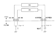
- FIG. 12 there are generally various circuit power supplies and GNDs in an LSI. Even if such power supply and GND are separated from each other in the circuits in the LSI, as shown in FIG. 13, they are short-circuited on the substrate on which the LSI chip is mounted. More specifically, since the short circuit at this time is via a wiring resistance as shown in FIG. 14, the common impedance between the power supply and GND of each circuit is set according to the current flowing through each circuit. Will affect each other.
- the power supply and GND that are separated from each other among the circuits in the source driver are FPC They are interconnected with the same wiring on the top and on the PWB.
- a current corresponding to the power supply and GND on the FPC and PWB also flows, and on the FPC and A voltage drop due to wiring resistance occurs in the power supply and GND on the PWB.
- the other circuit of the source driver since the other circuit of the source driver must operate using the power supply and the GND in which the voltage drop has occurred on the FPC and the PWB, the other circuit is affected by the circuit.
- the power supply and GND outside the chip are wiring on the display panel 2, so that the wiring resistance is extremely large and the voltage drop due to the common impedance. This seriously affects the source driver 4.
- the rising timing of the control pulses of the switches SSW1, SSW2, and SSW3 (corresponding to the switches SWR, SWG, and SWB in FIG. 6) that sequentially connect the RGB data signal lines to the source driver.
- a large current Ivdd flows through the power supply and GND used by each.
- a switch that connects the output of the source driver 4 to the data signal lines.
- Inrush current caused by charging the data signal line to the polarity opposite to the previous polarity flows at the rising timing of the control pulse of SSW2 and SSW3).
- SSW1 source output to a data signal line by line sequential driving, each time a source output for inverting the polarity is started from the source driver 4, the data signal line is charged by reversing the previous polarity. Current flows.
- an inrush current flows by charging the common electrode COM to a polarity opposite to the previous polarity.
- the inrush current described above extends to the current Ivdd flowing through the power supply and GND.
- the power supply voltage AD-VDD used by the AD conversion circuit and the reference voltages VREF and GND generated using the power supply voltage fluctuate at the timing when the current Ivdd flows. Therefore, if AD conversion is performed at a timing when the voltage fluctuates, there is a possibility that a correct AD conversion result cannot be obtained by operating using the voltage on which the noise is superimposed.
- AD conversion by the AD conversion circuit 45 is performed in the first period in which the large current Ivdd is not generated.
- the source driver 4 captures both the source output and the sensor output by using a common terminal for both in a time-sharing manner. Therefore, sampling for AD conversion is performed by capturing the sensor output. Although it will be performed in a period, sampling and AD conversion may not be performed continuously and may be separated. Therefore, once sampling is performed, AD conversion may be performed outside the sensor output capturing period.
- AD conversion is performed in the first period within the period t1.
- the period t1 is the maximum range of the first period. Note that the start timing of the first period in this case may be after the switching timing from the ON state to the OFF state of the last switch (SSW 3 in FIG. 1) through all colors for outputting the data signal to the data signal line. .
- the AD conversion is performed while avoiding the period of outputting the data signal to the data signal line, thereby avoiding the rise timing of the control pulses of the switches SSW1, SSW2, and SSW3.
- the first period corresponds to one selection period of the scanning signal line immediately after the RGB source output to each data signal line corresponding to one selection period of the scanning signal line is completed, for example. What is necessary is just to set within the period t1 'until the time of starting RGB source output to each data signal line for the first time. In general, the point in time when RGB source output corresponding to one selection period of the scanning signal line is first started is after the voltage change timing of the common electrode COM corresponding to the one selection period.
- AD conversion By performing AD conversion during the above period, AD conversion can be performed while avoiding the timing at which noise shown in FIG. 1 occurs, so that a correct AD conversion result of sensor output can be obtained.
- the AD conversion in FIG. 2 is similar to that in FIG. 1 as the periods t1 and t1 ′ during which AD conversion can be performed, but sensor outputs of two different pixels are time-sequentially input to the same AD conversion input unit. By switching and sequentially inputting, two types of AD conversion are performed during the period.
- Such a configuration can be realized, for example, in FIG. 6 as a configuration in which the switch unit 47b is configured as a double throw switch, and AD conversion input paths of adjacent pixels can be selectively connected by the same switch unit 47b. In this case, the switch unit 47b connected to the adjacent terminal P is omitted.
- the AD conversion of FIG. 3 is for a display device that performs line-sequential driving that outputs the same data signal to each data signal line within one horizontal period without outputting RGB data signals in a time division in one horizontal period.
- the period for performing AD conversion is a period for outputting a data signal to the data signal line and a period for avoiding the voltage change timing when the common electrode COM is driven.
- AD is output in a first period within a period t2 from the time when source output to each data signal line corresponding to one selection period of the scanning signal line ends until the voltage change timing of the common electrode COM occurs. Conversion is in progress.
- the period t2 is the maximum range of the first period.
- the first period corresponds to one selection period of the scanning signal line immediately after the RGB source output to each data signal line corresponding to one selection period of the scanning signal line is completed, for example. What is necessary is just to set within the period t2 'until the time of starting the RGB source output to each data signal line.
- FIG. 3 shows an example in which the period t2 ′ coincides with the period t2. However, the point in time when the RGB source output corresponding to one selection period of the scanning signal line is started is generally in the one selection period. It is after the voltage change timing of the corresponding common electrode COM.
- the 20 is performed immediately after the last source output Vd to each data signal line corresponding to one selection period of the scanning signal line in a display device that performs dot sequential driving for each predetermined number of data signal lines.
- This method is performed in the first period within the period until the voltage change timing of the common electrode COM.
- AD conversion is performed in the first period within the period t3 from the middle of the output period of the B source output Vd to the data signal line to the voltage change timing of the common electrode COM immediately after. .
- the period t3 is the maximum range of the first period. In this case, if the first period is set within the source output period, the sensor output Vs is sampled in advance outside the source output period.
- the scanning signal line of the scanning signal line immediately after the last source output Vd to each data signal line corresponding to one selection period of the scanning signal line is displayed in the same manner as in FIG.
- the RGB source output to each data signal line corresponding to one selection period may be set within a period up to the time when it is first started.
- the AD conversion shown in FIG. 21 is completed from the middle of one source output Vd to each data signal line corresponding to one selection period of the scanning signal line in a display device that performs dot sequential driving for each predetermined number of data signal lines.
- This method is performed in the first period within the period up to.
- AD conversion is performed in a first period within a period t4 from the middle of the output period of the G source output Vd to the data signal line to the end point of the G source output Vd.
- the period t4 is the maximum range of the first period.
- the sensor output Vs is sampled in advance outside the source output period.
- a period similar to the period t4 may be set in the output period of the R and B data signals to the data signal line.
- one source output Vd other than the last to each data signal line corresponding to one selection period of the scanning signal line is halfway.
- a / D conversion is performed.
- the period t5 is the maximum range of the first period.
- the sensor output Vs is sampled in advance outside the source output period. Further, there is no source output Vd between the end time of the G source output Vd from the source driver 4 and the start time of the B source output Vd from the source driver 4 as in the period indicated by N. There may be a period in which the potential of the data signal line that has finished outputting the source output Vd is indefinite. The period from the middle of the output period of the R source output Vd to the data signal line to the start point of the G source output Vd to the data signal line may be set to the same period as the period t5.
- the output period of the source output Vd to the data signal line including the first period is set to be longer than the respective output periods of the source output Vd to the other data signal lines, and AD
- the conversion can be performed in a period when the current and voltage are more stable.
- FIG. 20 and FIG. 21 can be applied to a display device that performs source output Vd by line-sequential driving.
- the common output immediately after the middle of the source output Vd to each data signal line corresponding to one selection period of the scanning signal line is used.
- AD conversion is performed in the first period within the period until the voltage change timing of the electrode COM and the common electrode COM is not driven, the source output to each data signal line corresponding to one selection period of the scanning signal line AD conversion is performed during the first period within the period from the middle of Vd to the point immediately after the start of RGB source output to each data signal line corresponding to one selection period of the scanning signal line.
- the first period in the period from the middle of the source output Vd to each data signal line corresponding to one selection period of the scanning signal line to the end point is used.
- a / D conversion is performed.
- the first period is set so that the AD conversion of the sensor output is started after (when the source output of B ends after the falling timing of the control pulse of the switch SSW3). May be.
- the fall timing is delayed. Since the falling edge of the control pulse is surely completed at the end of the source output, it is possible to reliably avoid the AD conversion from interfering with the output of the source output Vd to the data signal line.
- the number of divisions when the data signal line is driven in a time division manner is not limited to the three divisions shown in FIGS. 1, 2, 20, 21, and 22, and any division number may be used.
- Fig. 8 shows the circuit connections during the sensor output sampling period.
- the switch SW1 corresponds to the switch unit 47b in FIG. Inside the AD conversion circuit 45, the switch SW2 and the hold capacitor C1 are connected in series between the input terminal of the AD conversion circuit 45 connected to one end of the switch SW1 and the input of the comparator 45a. Between the input terminal and the switch SW2, a constant current source 45x for supplying a constant current toward GND is provided. A connection point M between the switch SW2 and the hold capacitor C1 is connected to the output of the DA converter 45b via the switch SW3.
- the control logic 45f collectively represents the register 45d and the sequence control circuit 45e in FIG. A connection point N between the hold capacitor C1 and the input of the comparator 45a is connected to the reference voltage VREF via the switch SW4.
- the operation of the buffer 47a is stopped and the switch SW1 is turned on.
- the switches SW2 and SW4 are turned on and the switch SW3 is turned off, and the sensor output is sampled by accumulating charges corresponding to the sensor output in the hold capacitor C1.
- the hold period starts, the hold switches SW1 to SW4 are turned off, and the sensor output is held by the hold capacitor C1.
- the buffer 47a can be operated. Therefore, after the sensor output is held, AD conversion is performed until any time when AD conversion is possible. Can wait.
- the AD conversion period starts, and the switch SW3 is turned on while the switches SW1, SW2, and SW4 are kept off.
- the operation described with reference to FIG. 7 is performed.
- the switch SW3 is once turned off, each bit is determined, and then the switch SW3 is turned on again.
- the AD conversion is completed, and the connection relationship shown in FIG. 8 is restored to sample the next sensor output.
- the DA converter 45b is used for the AD converter circuit 45.
- an AD converter circuit that performs AD conversion according to the principle shown in FIG. 11 is provided instead of the AD converter circuit using the DA converter 45b. You can also.
- the comparator compares the sensor voltage with a temporally changing voltage E, and as shown in FIG. 11B, the comparator changes the output from Low to High. The digital value is determined according to the length of time.
- the present embodiment has been described above. It is obvious that the present invention can be applied to any other display device such as an EL display device and a display device using a dielectric liquid.
- the optical sensor may output other signals such as a current corresponding to the detected light intensity.
- the display device of the present invention is provided with the data signal line driving circuit according to the COG (Chip On Glass) method, and with the optical sensor that outputs a signal corresponding to the detected light intensity in the display region.
- the data signal line driving circuit includes an analog-digital conversion circuit that performs analog-digital conversion on the output of the photosensor, and is driven so that the voltage of the common electrode changes.
- the analog-to-digital conversion circuit performs a first analog-to-digital conversion of the output of the photosensor while avoiding a period in which a data signal is output to each data signal line and a voltage change timing by driving the common electrode. During the period.
- the display device of the present invention is provided with the data signal line driving circuit according to the COG (Chip On Glass) method, and with the optical sensor that outputs a signal corresponding to the detected light intensity in the display region.
- the data signal line driving circuit includes an analog-digital conversion circuit that performs analog-digital conversion on the output of the photosensor, and the voltage of the common electrode is driven to change.
- the analog-to-digital conversion circuit performs analog-to-digital conversion of the output of the photosensor in a first period avoiding a period in which a data signal is output to the data signal line.
- the driving method of the display device of the present invention includes the data signal line driving circuit according to the COG (Chip On ⁇ Glass) method and the optical sensor that outputs a signal corresponding to the detected light intensity in the display region.
- the data signal line driving circuit is made to perform analog-digital conversion of the output of the photosensor.
- the driving method of the display device of the present invention includes the data signal line driving circuit according to the COG (Chip On ⁇ Glass) method and the optical sensor that outputs a signal corresponding to the detected light intensity in the display region.
- a driving method of a display device for driving an active matrix display device wherein the voltage of the common electrode is not driven to change, and a period in which a data signal is output to the data signal line is avoided. In the first period, the data signal line driving circuit is caused to perform analog-digital conversion of the output of the photosensor.
- the present invention can be particularly suitably used for display devices such as liquid crystal display devices and EL display devices.
- Liquid crystal display device display device
- Source driver data signal line drive circuit
- AD conversion circuit analog-digital conversion circuit
- Photodiode light sensor
Landscapes
- Engineering & Computer Science (AREA)
- General Engineering & Computer Science (AREA)
- Theoretical Computer Science (AREA)
- Human Computer Interaction (AREA)
- Physics & Mathematics (AREA)
- General Physics & Mathematics (AREA)
- Control Of Indicators Other Than Cathode Ray Tubes (AREA)
- Liquid Crystal Display Device Control (AREA)
- Liquid Crystal (AREA)
Abstract
Priority Applications (4)
| Application Number | Priority Date | Filing Date | Title |
|---|---|---|---|
| EP09729828A EP2261885A4 (fr) | 2008-04-11 | 2009-01-14 | Dispositif d'affichage et procédé de commande de dispositif d'affichage |
| CN2009801034375A CN101933079B (zh) | 2008-04-11 | 2009-01-14 | 显示装置和显示装置的驱动方法 |
| JP2010507182A JP5053434B2 (ja) | 2008-04-11 | 2009-01-14 | 表示装置および表示装置の駆動方法 |
| US12/864,099 US20100295833A1 (en) | 2008-04-11 | 2009-01-14 | Display device and method of driving display device |
Applications Claiming Priority (2)
| Application Number | Priority Date | Filing Date | Title |
|---|---|---|---|
| JP2008-104017 | 2008-04-11 | ||
| JP2008104017 | 2008-04-11 |
Publications (1)
| Publication Number | Publication Date |
|---|---|
| WO2009125614A1 true WO2009125614A1 (fr) | 2009-10-15 |
Family
ID=41161750
Family Applications (1)
| Application Number | Title | Priority Date | Filing Date |
|---|---|---|---|
| PCT/JP2009/050356 WO2009125614A1 (fr) | 2008-04-11 | 2009-01-14 | Dispositif d'affichage et procédé de commande de dispositif d'affichage |
Country Status (5)
| Country | Link |
|---|---|
| US (1) | US20100295833A1 (fr) |
| EP (1) | EP2261885A4 (fr) |
| JP (1) | JP5053434B2 (fr) |
| CN (1) | CN101933079B (fr) |
| WO (1) | WO2009125614A1 (fr) |
Cited By (3)
| Publication number | Priority date | Publication date | Assignee | Title |
|---|---|---|---|---|
| WO2013129333A1 (fr) * | 2012-03-02 | 2013-09-06 | シャープ株式会社 | Dispositif d'affichage |
| JP2013200557A (ja) * | 2012-03-23 | 2013-10-03 | Lg Display Co Ltd | 液晶表示装置 |
| WO2018088315A1 (fr) * | 2016-11-11 | 2018-05-17 | シャープ株式会社 | Dispositif d'affichage avec capteur tactile et procédé de commande associé |
Families Citing this family (12)
| Publication number | Priority date | Publication date | Assignee | Title |
|---|---|---|---|---|
| CN101925943B (zh) * | 2008-04-11 | 2012-08-29 | 夏普株式会社 | 显示装置的驱动电路和显示装置 |
| US9665620B2 (en) | 2010-01-15 | 2017-05-30 | Ab Initio Technology Llc | Managing data queries |
| US9116955B2 (en) | 2011-05-02 | 2015-08-25 | Ab Initio Technology Llc | Managing data queries |
| CN105027189B (zh) * | 2013-03-08 | 2017-07-11 | 夏普株式会社 | 液晶显示装置及其驱动方法 |
| TWI532031B (zh) * | 2013-08-12 | 2016-05-01 | 聯詠科技股份有限公司 | 源極驅動器及其畫素電壓極性決定方法 |
| CN105793818B (zh) | 2013-12-06 | 2019-09-17 | 起元科技有限公司 | 源代码翻译 |
| KR101615813B1 (ko) * | 2014-05-30 | 2016-05-13 | 엘지디스플레이 주식회사 | 시분할 구동방식의 터치 센싱 장치 |
| US10437819B2 (en) | 2014-11-14 | 2019-10-08 | Ab Initio Technology Llc | Processing queries containing a union-type operation |
| JP6398679B2 (ja) * | 2014-12-12 | 2018-10-03 | Smk株式会社 | 撮像装置 |
| US10417281B2 (en) * | 2015-02-18 | 2019-09-17 | Ab Initio Technology Llc | Querying a data source on a network |
| TWI678694B (zh) * | 2018-09-14 | 2019-12-01 | 友達光電股份有限公司 | 顯示裝置驅動方法以及顯示裝置 |
| US11093223B2 (en) | 2019-07-18 | 2021-08-17 | Ab Initio Technology Llc | Automatically converting a program written in a procedural programming language into a dataflow graph and related systems and methods |
Citations (9)
| Publication number | Priority date | Publication date | Assignee | Title |
|---|---|---|---|---|
| JPH1091343A (ja) | 1996-09-17 | 1998-04-10 | Toshiba Corp | ペン入力表示装置 |
| JP2000089912A (ja) | 1998-09-14 | 2000-03-31 | Sharp Corp | 液晶表示装置 |
| JP2002062856A (ja) | 2000-06-06 | 2002-02-28 | Semiconductor Energy Lab Co Ltd | 表示装置及びその作製方法 |
| JP2005148285A (ja) | 2003-11-13 | 2005-06-09 | Sony Corp | 表示装置およびその駆動方法 |
| JP2005327106A (ja) | 2004-05-14 | 2005-11-24 | Toshiba Matsushita Display Technology Co Ltd | インプットセンサ内蔵ディスプレイ装置及びその駆動方法 |
| JP2006133786A (ja) | 2004-11-08 | 2006-05-25 | Samsung Electronics Co Ltd | 表示装置及び表示装置用駆動装置 |
| JP2006267967A (ja) | 2005-03-25 | 2006-10-05 | Toshiba Matsushita Display Technology Co Ltd | 平面表示装置 |
| JP2008015755A (ja) * | 2006-07-05 | 2008-01-24 | Toshiba Matsushita Display Technology Co Ltd | センサ内蔵表示装置 |
| JP2008027292A (ja) * | 2006-07-24 | 2008-02-07 | Toshiba Matsushita Display Technology Co Ltd | 表示装置 |
Family Cites Families (22)
| Publication number | Priority date | Publication date | Assignee | Title |
|---|---|---|---|---|
| EP0420568B1 (fr) * | 1989-09-28 | 1996-02-28 | Matsushita Electric Industrial Co., Ltd. | Dispositif numérique de convergence |
| US5510807A (en) * | 1993-01-05 | 1996-04-23 | Yuen Foong Yu H.K. Co., Ltd. | Data driver circuit and associated method for use with scanned LCD video display |
| DE69837874T2 (de) * | 1997-04-22 | 2008-02-07 | Matsushita Electric Industrial Co. Ltd. | Flüssigkristallanzeige mit bildeinlesefunktion, bildeinleseverfahren und herstellungsverfahren |
| US6995753B2 (en) * | 2000-06-06 | 2006-02-07 | Semiconductor Energy Laboratory Co., Ltd. | Display device and method of manufacturing the same |
| CN100378551C (zh) * | 2001-10-22 | 2008-04-02 | 三星电子株式会社 | 液晶显示器及其制造方法 |
| US7205988B2 (en) * | 2002-07-12 | 2007-04-17 | Toshiba Matsushita Display Technology Co., Ltd. | Display device |
| KR100983524B1 (ko) * | 2003-12-01 | 2010-09-24 | 삼성전자주식회사 | 광감지 패널과, 이를 갖는 광감지 장치 및 이의 구동 방법 |
| US7612818B2 (en) * | 2004-03-29 | 2009-11-03 | Toshiba Matsushita Display Technology Co., Ltd. | Input sensor containing display device and method for driving the same |
| US7633539B2 (en) * | 2004-06-07 | 2009-12-15 | Canon Kabushiki Kaisha | Image pickup device with analog-to-digital converter |
| JP2006244218A (ja) * | 2005-03-04 | 2006-09-14 | Toshiba Matsushita Display Technology Co Ltd | センサ内蔵表示装置 |
| JP4645822B2 (ja) * | 2005-04-19 | 2011-03-09 | ソニー株式会社 | 画像表示装置および物体の検出方法 |
| US7636078B2 (en) * | 2005-05-20 | 2009-12-22 | Semiconductor Energy Laboratory Co., Ltd. | Display device and electronic device |
| JP4618026B2 (ja) * | 2005-07-12 | 2011-01-26 | ソニー株式会社 | 表示装置及び表示および受光を行う表示装置を用いた検出方法 |
| JP2007072318A (ja) * | 2005-09-08 | 2007-03-22 | Toshiba Matsushita Display Technology Co Ltd | 表示装置 |
| JP2007163877A (ja) * | 2005-12-14 | 2007-06-28 | Toshiba Matsushita Display Technology Co Ltd | アレイ基板及び表示装置 |
| DE602006018423D1 (de) * | 2006-05-02 | 2011-01-05 | Chimei Innolux Corp | Organische Elektrolumineszenzvorrichtung und Herstellungsverfahren |
| US8570468B2 (en) * | 2006-06-30 | 2013-10-29 | Lg Display Co., Ltd. | Liquid crystal display device and method of fabricating the same |
| WO2008007480A1 (fr) * | 2006-07-14 | 2008-01-17 | Sharp Kabushiki Kaisha | Substrat à matrice active et dispositif d'affichage utilisant celui-ci |
| KR20080010551A (ko) * | 2006-07-27 | 2008-01-31 | 삼성전자주식회사 | 표시 장치의 구동 장치 및 이를 포함하는 표시 장치 |
| US7443331B2 (en) * | 2006-08-22 | 2008-10-28 | Texas Instruments Incorporated | Multiple-bank CMOS image sensor system and method |
| WO2008126768A1 (fr) * | 2007-04-09 | 2008-10-23 | Sharp Kabushiki Kaisha | Dispositif d'affichage |
| CN101925943B (zh) * | 2008-04-11 | 2012-08-29 | 夏普株式会社 | 显示装置的驱动电路和显示装置 |
-
2009
- 2009-01-14 CN CN2009801034375A patent/CN101933079B/zh not_active Expired - Fee Related
- 2009-01-14 US US12/864,099 patent/US20100295833A1/en not_active Abandoned
- 2009-01-14 JP JP2010507182A patent/JP5053434B2/ja not_active Expired - Fee Related
- 2009-01-14 WO PCT/JP2009/050356 patent/WO2009125614A1/fr active Application Filing
- 2009-01-14 EP EP09729828A patent/EP2261885A4/fr not_active Withdrawn
Patent Citations (9)
| Publication number | Priority date | Publication date | Assignee | Title |
|---|---|---|---|---|
| JPH1091343A (ja) | 1996-09-17 | 1998-04-10 | Toshiba Corp | ペン入力表示装置 |
| JP2000089912A (ja) | 1998-09-14 | 2000-03-31 | Sharp Corp | 液晶表示装置 |
| JP2002062856A (ja) | 2000-06-06 | 2002-02-28 | Semiconductor Energy Lab Co Ltd | 表示装置及びその作製方法 |
| JP2005148285A (ja) | 2003-11-13 | 2005-06-09 | Sony Corp | 表示装置およびその駆動方法 |
| JP2005327106A (ja) | 2004-05-14 | 2005-11-24 | Toshiba Matsushita Display Technology Co Ltd | インプットセンサ内蔵ディスプレイ装置及びその駆動方法 |
| JP2006133786A (ja) | 2004-11-08 | 2006-05-25 | Samsung Electronics Co Ltd | 表示装置及び表示装置用駆動装置 |
| JP2006267967A (ja) | 2005-03-25 | 2006-10-05 | Toshiba Matsushita Display Technology Co Ltd | 平面表示装置 |
| JP2008015755A (ja) * | 2006-07-05 | 2008-01-24 | Toshiba Matsushita Display Technology Co Ltd | センサ内蔵表示装置 |
| JP2008027292A (ja) * | 2006-07-24 | 2008-02-07 | Toshiba Matsushita Display Technology Co Ltd | 表示装置 |
Non-Patent Citations (1)
| Title |
|---|
| See also references of EP2261885A4 * |
Cited By (6)
| Publication number | Priority date | Publication date | Assignee | Title |
|---|---|---|---|---|
| WO2013129333A1 (fr) * | 2012-03-02 | 2013-09-06 | シャープ株式会社 | Dispositif d'affichage |
| JPWO2013129333A1 (ja) * | 2012-03-02 | 2015-07-30 | シャープ株式会社 | 表示装置 |
| US9411454B2 (en) | 2012-03-02 | 2016-08-09 | Sharp Kabushiki Kaisha | Display device |
| JP2013200557A (ja) * | 2012-03-23 | 2013-10-03 | Lg Display Co Ltd | 液晶表示装置 |
| US9390680B2 (en) | 2012-03-23 | 2016-07-12 | Lg Display Co., Ltd. | Liquid crystal display device |
| WO2018088315A1 (fr) * | 2016-11-11 | 2018-05-17 | シャープ株式会社 | Dispositif d'affichage avec capteur tactile et procédé de commande associé |
Also Published As
| Publication number | Publication date |
|---|---|
| EP2261885A4 (fr) | 2011-08-24 |
| JPWO2009125614A1 (ja) | 2011-08-04 |
| EP2261885A1 (fr) | 2010-12-15 |
| US20100295833A1 (en) | 2010-11-25 |
| CN101933079A (zh) | 2010-12-29 |
| JP5053434B2 (ja) | 2012-10-17 |
| CN101933079B (zh) | 2012-11-28 |
Similar Documents
| Publication | Publication Date | Title |
|---|---|---|
| JP5053434B2 (ja) | 表示装置および表示装置の駆動方法 | |
| JP5179572B2 (ja) | 表示装置の駆動回路および表示装置 | |
| JP4887657B2 (ja) | アクティブマトリクス型表示装置及びその駆動方法 | |
| US10490154B2 (en) | Electro-optical device and electronic device | |
| US20080100603A1 (en) | Driving method of liquid crystal display apparatus and driving circuit of the same | |
| US20090009510A1 (en) | Data line driving circuit, display device and method of driving data line | |
| KR20160130028A (ko) | 표시장치 | |
| KR20140128775A (ko) | 전력 소모를 줄일 수 있는 전하 공유 방법과 상기 방법을 수행할 수 있는 장치들 | |
| US20070052874A1 (en) | Display apparatus including sensor in pixel | |
| US7692615B2 (en) | Display driver, electro-optical device, and method of driving electro-optical device | |
| US10152907B2 (en) | Circuit device, electro-optical apparatus, and electronic instrument | |
| US6628261B1 (en) | Liquid crystal display panel drive circuit and liquid crystal display apparatus having two sample/hold circuits coupled to each signal line | |
| US20090096816A1 (en) | Data driver, integrated circuit device, and electronic instrument | |
| US20180090085A1 (en) | Electro-optical device, method of controlling electro-optical device, and electronic apparatus | |
| JP7114875B2 (ja) | 電気光学装置、電気光学装置の制御方法および電子機器 | |
| US20070132620A1 (en) | Array substrate and display device | |
| US7616183B2 (en) | Source driving circuit of display device and source driving method thereof | |
| US20050243049A1 (en) | Semiconductor integrated circuit device | |
| US10290278B2 (en) | Electrooptical device, electronic device, and control method of electrooptical device | |
| JP2010102146A (ja) | 液晶表示装置のドライブ装置および液晶表示装置 | |
| KR102581718B1 (ko) | 표시 장치 | |
| JP2009168842A (ja) | 基準電圧生成回路、ドライバ、電気光学装置及び電子機器 | |
| US20190340994A1 (en) | Source driver and a display driver integrated circuit | |
| JP6699298B2 (ja) | 電気光学装置、電気光学装置の制御方法および電子機器 | |
| CN113614819B (zh) | 显示装置 |
Legal Events
| Date | Code | Title | Description |
|---|---|---|---|
| WWE | Wipo information: entry into national phase |
Ref document number: 200980103437.5 Country of ref document: CN |
|
| 121 | Ep: the epo has been informed by wipo that ep was designated in this application |
Ref document number: 09729828 Country of ref document: EP Kind code of ref document: A1 |
|
| WWE | Wipo information: entry into national phase |
Ref document number: 2010507182 Country of ref document: JP |
|
| WWE | Wipo information: entry into national phase |
Ref document number: 2009729828 Country of ref document: EP |
|
| WWE | Wipo information: entry into national phase |
Ref document number: 12864099 Country of ref document: US |
|
| NENP | Non-entry into the national phase |
Ref country code: DE |