WO2009125515A1 - 液晶表示装置 - Google Patents
液晶表示装置 Download PDFInfo
- Publication number
- WO2009125515A1 WO2009125515A1 PCT/JP2008/071698 JP2008071698W WO2009125515A1 WO 2009125515 A1 WO2009125515 A1 WO 2009125515A1 JP 2008071698 W JP2008071698 W JP 2008071698W WO 2009125515 A1 WO2009125515 A1 WO 2009125515A1
- Authority
- WO
- WIPO (PCT)
- Prior art keywords
- liquid crystal
- birefringent layer
- polarizer
- crystal display
- plate
- Prior art date
Links
Images


Classifications
-
- G—PHYSICS
- G02—OPTICS
- G02F—OPTICAL DEVICES OR ARRANGEMENTS FOR THE CONTROL OF LIGHT BY MODIFICATION OF THE OPTICAL PROPERTIES OF THE MEDIA OF THE ELEMENTS INVOLVED THEREIN; NON-LINEAR OPTICS; FREQUENCY-CHANGING OF LIGHT; OPTICAL LOGIC ELEMENTS; OPTICAL ANALOGUE/DIGITAL CONVERTERS
- G02F1/00—Devices or arrangements for the control of the intensity, colour, phase, polarisation or direction of light arriving from an independent light source, e.g. switching, gating or modulating; Non-linear optics
- G02F1/01—Devices or arrangements for the control of the intensity, colour, phase, polarisation or direction of light arriving from an independent light source, e.g. switching, gating or modulating; Non-linear optics for the control of the intensity, phase, polarisation or colour
- G02F1/13—Devices or arrangements for the control of the intensity, colour, phase, polarisation or direction of light arriving from an independent light source, e.g. switching, gating or modulating; Non-linear optics for the control of the intensity, phase, polarisation or colour based on liquid crystals, e.g. single liquid crystal display cells
- G02F1/133—Constructional arrangements; Operation of liquid crystal cells; Circuit arrangements
- G02F1/1333—Constructional arrangements; Manufacturing methods
- G02F1/1335—Structural association of cells with optical devices, e.g. polarisers or reflectors
- G02F1/13363—Birefringent elements, e.g. for optical compensation
-
- G—PHYSICS
- G02—OPTICS
- G02B—OPTICAL ELEMENTS, SYSTEMS OR APPARATUS
- G02B27/00—Optical systems or apparatus not provided for by any of the groups G02B1/00 - G02B26/00, G02B30/00
- G02B27/28—Optical systems or apparatus not provided for by any of the groups G02B1/00 - G02B26/00, G02B30/00 for polarising
-
- G—PHYSICS
- G02—OPTICS
- G02B—OPTICAL ELEMENTS, SYSTEMS OR APPARATUS
- G02B5/00—Optical elements other than lenses
- G02B5/30—Polarising elements
- G02B5/3083—Birefringent or phase retarding elements
-
- G—PHYSICS
- G02—OPTICS
- G02F—OPTICAL DEVICES OR ARRANGEMENTS FOR THE CONTROL OF LIGHT BY MODIFICATION OF THE OPTICAL PROPERTIES OF THE MEDIA OF THE ELEMENTS INVOLVED THEREIN; NON-LINEAR OPTICS; FREQUENCY-CHANGING OF LIGHT; OPTICAL LOGIC ELEMENTS; OPTICAL ANALOGUE/DIGITAL CONVERTERS
- G02F1/00—Devices or arrangements for the control of the intensity, colour, phase, polarisation or direction of light arriving from an independent light source, e.g. switching, gating or modulating; Non-linear optics
- G02F1/01—Devices or arrangements for the control of the intensity, colour, phase, polarisation or direction of light arriving from an independent light source, e.g. switching, gating or modulating; Non-linear optics for the control of the intensity, phase, polarisation or colour
- G02F1/13—Devices or arrangements for the control of the intensity, colour, phase, polarisation or direction of light arriving from an independent light source, e.g. switching, gating or modulating; Non-linear optics for the control of the intensity, phase, polarisation or colour based on liquid crystals, e.g. single liquid crystal display cells
- G02F1/133—Constructional arrangements; Operation of liquid crystal cells; Circuit arrangements
- G02F1/1333—Constructional arrangements; Manufacturing methods
- G02F1/1335—Structural association of cells with optical devices, e.g. polarisers or reflectors
- G02F1/133528—Polarisers
-
- G—PHYSICS
- G02—OPTICS
- G02F—OPTICAL DEVICES OR ARRANGEMENTS FOR THE CONTROL OF LIGHT BY MODIFICATION OF THE OPTICAL PROPERTIES OF THE MEDIA OF THE ELEMENTS INVOLVED THEREIN; NON-LINEAR OPTICS; FREQUENCY-CHANGING OF LIGHT; OPTICAL LOGIC ELEMENTS; OPTICAL ANALOGUE/DIGITAL CONVERTERS
- G02F1/00—Devices or arrangements for the control of the intensity, colour, phase, polarisation or direction of light arriving from an independent light source, e.g. switching, gating or modulating; Non-linear optics
- G02F1/01—Devices or arrangements for the control of the intensity, colour, phase, polarisation or direction of light arriving from an independent light source, e.g. switching, gating or modulating; Non-linear optics for the control of the intensity, phase, polarisation or colour
- G02F1/13—Devices or arrangements for the control of the intensity, colour, phase, polarisation or direction of light arriving from an independent light source, e.g. switching, gating or modulating; Non-linear optics for the control of the intensity, phase, polarisation or colour based on liquid crystals, e.g. single liquid crystal display cells
- G02F1/133—Constructional arrangements; Operation of liquid crystal cells; Circuit arrangements
- G02F1/1333—Constructional arrangements; Manufacturing methods
- G02F1/1335—Structural association of cells with optical devices, e.g. polarisers or reflectors
- G02F1/13363—Birefringent elements, e.g. for optical compensation
- G02F1/133638—Waveplates, i.e. plates with a retardation value of lambda/n
-
- G—PHYSICS
- G02—OPTICS
- G02F—OPTICAL DEVICES OR ARRANGEMENTS FOR THE CONTROL OF LIGHT BY MODIFICATION OF THE OPTICAL PROPERTIES OF THE MEDIA OF THE ELEMENTS INVOLVED THEREIN; NON-LINEAR OPTICS; FREQUENCY-CHANGING OF LIGHT; OPTICAL LOGIC ELEMENTS; OPTICAL ANALOGUE/DIGITAL CONVERTERS
- G02F2413/00—Indexing scheme related to G02F1/13363, i.e. to birefringent elements, e.g. for optical compensation, characterised by the number, position, orientation or value of the compensation plates
- G02F2413/04—Number of plates greater than or equal to 4
-
- G—PHYSICS
- G02—OPTICS
- G02F—OPTICAL DEVICES OR ARRANGEMENTS FOR THE CONTROL OF LIGHT BY MODIFICATION OF THE OPTICAL PROPERTIES OF THE MEDIA OF THE ELEMENTS INVOLVED THEREIN; NON-LINEAR OPTICS; FREQUENCY-CHANGING OF LIGHT; OPTICAL LOGIC ELEMENTS; OPTICAL ANALOGUE/DIGITAL CONVERTERS
- G02F2413/00—Indexing scheme related to G02F1/13363, i.e. to birefringent elements, e.g. for optical compensation, characterised by the number, position, orientation or value of the compensation plates
- G02F2413/06—Two plates on one side of the LC cell
-
- G—PHYSICS
- G02—OPTICS
- G02F—OPTICAL DEVICES OR ARRANGEMENTS FOR THE CONTROL OF LIGHT BY MODIFICATION OF THE OPTICAL PROPERTIES OF THE MEDIA OF THE ELEMENTS INVOLVED THEREIN; NON-LINEAR OPTICS; FREQUENCY-CHANGING OF LIGHT; OPTICAL LOGIC ELEMENTS; OPTICAL ANALOGUE/DIGITAL CONVERTERS
- G02F2413/00—Indexing scheme related to G02F1/13363, i.e. to birefringent elements, e.g. for optical compensation, characterised by the number, position, orientation or value of the compensation plates
- G02F2413/08—Indexing scheme related to G02F1/13363, i.e. to birefringent elements, e.g. for optical compensation, characterised by the number, position, orientation or value of the compensation plates with a particular optical axis orientation
Definitions
- the present invention relates to a liquid crystal display device. More specifically, the present invention relates to a VA (vertical alignment) mode liquid crystal display device using a circularly polarizing plate.
- VA vertical alignment
- TFT-LCDs TFT-type liquid crystal display devices
- the present invention is not limited to the TFT-LCD and can be applied to all liquid crystal display devices.
- a liquid crystal display device of a simple matrix method, a plasma address method, or the like It is also applicable to.
- the most widely used method in TFT-LCDs is a so-called TN mode in which liquid crystals having positive dielectric anisotropy are horizontally aligned between substrates facing each other.
- the TN mode liquid crystal display device is characterized in that the alignment direction of liquid crystal molecules adjacent to one substrate is twisted by 90 ° with respect to the alignment direction of liquid crystal molecules adjacent to the other substrate.
- an inexpensive manufacturing technique has been established and industrially matured, but it has been difficult to achieve a high contrast ratio.
- VA mode liquid crystal display device in which liquid crystals having negative dielectric anisotropy are vertically aligned between mutually opposing substrates.
- the liquid crystal molecules are aligned in a direction substantially perpendicular to the substrate surface, so that the liquid crystal cell hardly exhibits birefringence and optical rotation, and light is not It passes through the liquid crystal cell with almost no change in the polarization state.
- a substantially complete black display when no voltage is applied can be realized.
- the liquid crystal molecules tilt and become substantially parallel to the substrate, exhibiting a large birefringence and displaying white. Therefore, such a VA mode liquid crystal display device can easily achieve a very high contrast ratio.
- asymmetry occurs in the viewing angle characteristics of the liquid crystal display device.
- an alignment division type VA mode in which the tilt direction of liquid crystal molecules is divided into a plurality of directions, that is, a so-called MVA mode (multi-domain type VA mode) is widely used by providing an alignment control means such as a protrusion in a pixel.
- MVA mode multi-domain type VA mode
- the polarizer axis direction and the tilt direction of the liquid crystal molecules when a voltage is applied are usually set to form an angle of 45 °.
- the transmittance when the birefringent medium is sandwiched between crossed Nicol polarizers is expressed as follows: sin 2 (2 ⁇ ) where ⁇ (unit: rad) is an angle formed by the polarizer axis and the slow axis of the birefringent medium. This is because it is proportional to In a typical MVA mode, the tilt direction of liquid crystal molecules can be divided into four domains of 45 °, 135 °, 225 °, and 315 °. Even in such an MVA mode divided into four domains, schlieren orientation and orientation in an unintended direction are often observed in the vicinity of domain boundaries and orientation control means, which causes a loss of transmittance. Yes.
- a circular protrusion may be arranged at the center of the pixel and the liquid crystal molecules may be tilted in all directions, or tilted in a random direction without controlling the tilt direction at all. May be.
- a VA mode using a circularly polarizing plate is also referred to as a circularly polarized VA mode or a circularly polarized mode.
- a VA mode using a linear polarizing plate is also referred to as a linearly polarized VA mode or a linearly polarized mode.
- the circularly polarizing plate is typically composed of a combination of a linearly polarizing plate and a ⁇ / 4 plate.
- Patent Document 1 discloses the following method (A)
- Patent Document 2 discloses the following method (B)
- Patent Document 3 discloses the following method (C).
- A A method using a ⁇ / 4 plate satisfying a relationship of nx>ny> nz
- C A method using one or two ⁇ / 2 plates satisfying the relationship of nx>nz> ny in addition to the configuration of (B) Japanese Patent Laid-Open No. 2002-40428 JP 2003-207782 A JP 2003-186017 A
- the present invention has been made in view of the above situation, and an object thereof is to provide a liquid crystal display device that can be easily manufactured at low cost and can realize a high contrast ratio in a wide viewing angle range. To do.
- the inventors of the present invention have made various studies on a liquid crystal display device that can be easily manufactured at low cost and can achieve a high contrast ratio in a wide viewing angle range.
- a pair of polarizers with a crossed Nicol arrangement (The phase difference condition of the birefringent layer disposed between the first and second polarizers) was noted.
- Nz> 0.9, preferably Nz ⁇ 1.0 (satisfying the relationship of nx> ny ⁇ nz) is satisfied.
- the refractive layer and the second birefringent layer satisfying Nz ⁇ 0.1, preferably satisfying Nz ⁇ 0.0 (satisfying the relationship of nx ⁇ ny ⁇ nz). It has been found that the orthogonality of the first and second polarizers can be maintained in the oblique direction while maintaining the orthogonality of the first and second polarizers.
- the birefringent layers of the first and second types are materials having appropriate intrinsic birefringence, unlike the biaxial retardation film controlled to nx> nz> ny (0 ⁇ Nz ⁇ 1). It was found that it can be produced by a simple method by using. As a result, the inventors have conceived that the above problems can be solved brilliantly and have reached the present invention.
- the present invention includes a first polarizer, a first type birefringent layer, a first ⁇ / 4 plate, a liquid crystal cell, a second ⁇ / 4 plate, a second type birefringent layer, and the above
- a liquid crystal display device having a second polarizer whose absorption axis is orthogonal to the absorption axis of the first polarizer in this order, wherein the first type birefringent layer satisfies Nz> 0.9,
- the in-plane slow axis is orthogonal to the absorption axis of the first polarizer, and the first ⁇ / 4 plate has an in-plane slow axis of about the absorption axis of the first polarizer.
- the liquid crystal cell forms a black display by aligning the liquid crystal molecules in the liquid crystal cell perpendicularly to the substrate surface, and the second ⁇ / 4 plate has an in-plane slow phase.
- the axis is perpendicular to the in-plane slow axis of the first ⁇ / 4 plate, the second birefringent layer satisfies Nz ⁇ 0.1, and the in-plane slow axis is the second slow axis. Liquid parallel to the absorption axis of the polarizer A display device. The present invention is described in detail below.
- the liquid crystal display device of the present invention includes a first polarizer, a first type birefringent layer, a first ⁇ / 4 plate, a liquid crystal cell, a second ⁇ / 4 plate, a second type birefringent layer, and
- the second polarizer having an absorption axis orthogonal to the absorption axis of the first polarizer is provided in this order.
- the “polarizer” is an element having a function of changing natural light into linearly polarized light, and is synonymous with a polarizing plate and a polarizing film.
- a polyvinyl alcohol (PVA) film obtained by adsorbing and orienting an anisotropic material such as an iodine complex having dichroism can be used.
- a protective film such as a triacetyl cellulose (TAC) film is laminated on both sides of the PVA film, and this specification is used unless otherwise specified.
- TAC triacetyl cellulose
- the term “polarizer” refers only to an element having a polarizing function without including a protective film. Any of the first and second polarizers may be a polarizer (a polarizer on the back surface side) or an analyzer (a polarizer on the observation surface side).
- the liquid crystal display device of the present invention includes a first polarizer, a first type birefringent layer, a first ⁇ / 4 plate, a liquid crystal cell, a second ⁇ / 4 plate, a second type birefringent layer, and Moreover, when the substrate surface of the liquid crystal cell is viewed in plan, it may have a second polarizer whose absorption axis is orthogonal to the absorption axis of the first polarizer in this order.
- the absorption axis of the first polarizer and the absorption axis of the second polarizer are: It is preferable that the angle of 90 ° is formed when the substrate surface of the liquid crystal cell is viewed in plan. However, if the viewing angle can be compensated without reducing the contrast ratio in the front direction, the angle is 90. It may be slightly off from °. Specifically, when the substrate surface of the liquid crystal cell is viewed in plan, the absorption axis of the first polarizer and the absorption axis of the second polarizer are within the range of 90 ° to ⁇ 1 ° (89 to 91 °).
- first polarizer first type birefringent layer, first ⁇ / 4 plate, liquid crystal cell, second ⁇ / 4 plate, second type stacked in the liquid crystal display device of the present invention.
- the birefringent layer, the second polarizer, and the like may be simply placed, but are preferably laminated in a fixed state from the viewpoint of preventing deviation of the optical axis.
- the lamination method is not particularly limited, and for example, an appropriate method such as an adhesive method using an adhesive or a pressure-sensitive adhesive having excellent transparency can be adopted.
- the type of the adhesive or pressure-sensitive adhesive is not particularly limited, but a material that does not substantially exhibit optical anisotropy is preferable.
- the adhesive or pressure-sensitive adhesive is preferably one that does not require a high-temperature process during curing or drying, and requires a long curing process or drying time. Those that do not are preferred.
- the liquid crystal cell usually has a pair of substrates and a liquid crystal layer sandwiched between the pair of substrates.
- the liquid crystal cell according to the present invention is a vertical alignment (VA) mode liquid crystal cell that performs black display by aligning liquid crystal molecules in the liquid crystal cell perpendicularly to the substrate surface.
- VA modes include Multi-domain VA (MVA) mode, Continuous Pinwheel Alignment (CPA) mode, Patterned VA (PVA) mode, Biased Vertical Alignment (BVA) mode, Reverse TN mode, etc.
- the liquid crystal cell according to the present invention does not have to be a liquid crystal cell in which liquid crystal molecules are aligned strictly perpendicular to the substrate surface, but a liquid crystal in which liquid crystal molecules are aligned substantially perpendicular to the substrate surface.
- a cell may be sufficient and a liquid crystal molecule may have a pretilt angle.
- the liquid crystal cell may be one in which liquid crystal molecules are aligned perpendicular to the substrate surface in the absence of applied voltage.
- the liquid crystal display device of the present invention includes a first type birefringent layer, a first ⁇ / 4 plate, and a second ⁇ / 4 plate between a first polarizer and a second polarizer. And a second birefringent layer.
- the “birefringent layer” refers to a layer having optical anisotropy, and is synonymous with a retardation film, a retardation plate, an optically anisotropic layer, a birefringent medium, and the like.
- the “ ⁇ / 4 plate” means at least about a quarter wavelength with respect to light having a wavelength of 550 nm (more precisely, it is 137.5 nm, but it should be larger than 115 nm and smaller than 160 nm. )) And has the same anisotropy as ⁇ / 4 retardation film and ⁇ / 4 retardation plate.
- the first and second birefringent layers are not intended to provide a phase difference to light incident from the normal direction.
- the angle formed between the absorption axis of the first polarizer and the absorption axis of the second polarizer is apparently different from the front direction. Compensation is performed by the phase difference of the birefringent layer of the seed. That is, the first and second birefringent layers are intended to provide a phase difference only to light incident from an oblique direction and perform viewing angle compensation.
- the first and second birefringent layers in the present invention maintain the orthogonality of the first and second polarizers in the front direction, and the first and second in the oblique direction. This makes it possible to obtain the orthogonality of the polarizer, thereby improving the contrast ratio in the oblique direction and realizing a liquid crystal display device excellent in viewing angle characteristics.
- the liquid crystal display device of the present invention includes the first polarizer, the first type birefringent layer, the first ⁇ / 4 plate, the liquid crystal cell, the second ⁇ / 4 plate, and the second type birefringent layer.
- the second polarizer is provided as a constituent element, it is not particularly limited by other members.
- the first type birefringent layer satisfies Nz> 0.9, and the in-plane slow axis is orthogonal to the absorption axis of the first polarizer.
- the measurement wavelength of the main refractive index and the phase difference is 550 nm.
- the Nz coefficient of the first type birefringent layer is less than 1.0, the relationship of nx> nz> ny is satisfied, which may make it difficult to manufacture.
- a birefringent layer satisfying 1.0 ⁇ Nz can be easily manufactured by using a normal manufacturing method (for example, horizontal uniaxial stretching, vertical / horizontal biaxial stretching).
- the first birefringent layer satisfying 1.1 ⁇ Nz ⁇ 4.0 is typically subjected to general transverse uniaxial stretching or longitudinal and transverse biaxial stretching using a material having positive intrinsic birefringence. Can be manufactured more easily. From such a point, the first type birefringent layer is preferably made of a material having positive intrinsic birefringence.
- the in-plane slow axis is a roll-like phase difference.
- a polarizer film obtained by adsorbing and orienting an anisotropic material such as an iodine complex having dichroism on a PVA film is a roll-shaped polarizer having an absorption axis in a direction parallel to the longitudinal direction.
- Roll-to-roll bonding is possible so that the in-plane slow axis of the birefringent layer of the seed makes an angle of 90 ° with respect to the absorption axis of the first polarizer (perpendicular).
- the first type birefringent layer satisfies Nz> 0.9, and the in-plane slow axis is perpendicular to the absorption axis of the first polarizer when the substrate surface of the liquid crystal cell is viewed in plan. Good.
- the second birefringent layer satisfies Nz ⁇ 0.1, and the in-plane slow axis is parallel to the absorption axis of the second polarizer. If the Nz coefficient of the second birefringent layer is greater than 0.0, the relationship of nx> nz> ny may be satisfied, which may make it difficult to manufacture.
- the second birefringent layer satisfying Nz ⁇ 0.1 can be easily manufactured. More preferably, the second birefringent layer satisfies ⁇ 3.0 ⁇ Nz ⁇ ⁇ 0.1.
- the second birefringent layer satisfying ⁇ 3.0 ⁇ Nz ⁇ ⁇ 0.1 is typically prepared by subjecting a material having negative intrinsic birefringence to general longitudinal and transverse biaxial stretching. Is easier to manufacture. From such a point, the second birefringent layer is preferably made of a material having negative intrinsic birefringence.
- the in-plane slow axis is a roll shape. Since it is possible to make the direction 0 ° (parallel direction) to the longitudinal direction of the retardation film, the second birefringent layer and the second polarizer are roll-to-roll. It is preferable also from the point that it can paste.
- the second birefringent layer may satisfy Nz ⁇ 0.1, and the in-plane slow axis may be parallel to the absorption axis of the second polarizer when the substrate surface of the liquid crystal cell is viewed in plan. .
- the first type of birefringence In order to achieve a high contrast ratio in a wide viewing angle range (with viewing angle compensation) without reducing the contrast ratio in the front direction, basically, as described above, the first type of birefringence
- the in-plane slow axis of the layer and the absorption axis of the first polarizer form an angle of 90 °
- the in-plane slow axis of the second birefringent layer and the absorption axis of the second polarizer It is necessary to make an angle of 0 °. The reason is as follows.
- the birefringent layer In order not to reduce the contrast ratio in the front direction, (1) it is necessary that the birefringent layer does not function in the front direction, and in order to perform viewing angle compensation, (2) the birefringent layer is inclined. It needs to function effectively.
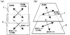
- the axial relationship between the birefringent layer and the polarizer is as follows: (a) the optical axis of the polarizer 1 and the optical axis of the birefringent layer 2 when observed from the front direction. Are parallel to each other (FIG. 1 (a)), and (b) the optical axis of the polarizer 1 and the optical axis of the birefringent layer 2 are orthogonal when viewed from the front direction (FIG. 2). It is necessary to satisfy any one of the relationships (a)).
- the “optical axis” is different from the optical axis in the strict sense referred to in the field of crystal optics, and is defined according to the following definition.
- the “optical axis” means a main axis corresponding to the main refractive index having the maximum absolute value of the difference from the average value among the three main refractive indexes of the birefringent layer. Therefore, even when the birefringent layer is optically biaxial, the “optical axis” of the birefringent layer is not two but one. Thus, the “optical axis” of the biaxial birefringent layer corresponds to a conventionally defined optical axis when it is optically approximated to a uniaxial birefringent layer.
- the effective transmission axis of the polarizer 1 when observed from the oblique direction and the vibration direction of the intrinsic polarization mode of the birefringent layer are parallel. But it must be not orthogonal.
- the optical axis of the polarizer 1 and the optical axis of the birefringent layer 2 are parallel as shown in (a)
- the polarizer 1 can be observed from any direction as shown in FIG. Since the effective transmission axis and one of the vibration directions of the two natural vibration modes of the birefringent layer 2 are parallel, the birefringent layer 2 does not function effectively.
- the polarizer 1 is inclined in the oblique direction as shown in FIG.
- the effective transmission axis of the birefringent layer 2 and the vibration direction of the intrinsic polarization mode of the birefringent layer 2 are neither parallel nor orthogonal, so that the birefringent layer 2 functions effectively.
- O-type polarizer refers to a direction that absorbs light oscillating in a specific direction (defined as an absorption axis) in the element plane and is orthogonal to the absorption axis in the element plane (defined as a transmission axis). It is a polarizer that transmits light that vibrates in the direction normal to the element plane and light that vibrates in the direction normal to the element plane. That is, the O-type polarizer is a polarizer having one absorption axis and two transmission axes, and the optical axis of the O-type polarizer faces the absorption axis.
- the angle may be slightly shifted from 90 °.
- the in-plane slow axis of the first kind of birefringent layer and the absorption axis of the first polarizer are 90 ° to ⁇ 1 ° (89 to 91). If it is within the range of °), the effects of the present invention are sufficiently obtained.
- the angle may slightly deviate from 0 °.
- the in-plane slow axis of the second birefringent layer and the absorption axis of the second polarizer are from 0 ° to ⁇ 1 ( ⁇ 1 to 1). If it is within the range of °) °, the effects of the present invention are sufficiently obtained.
- the first ⁇ / 4 plate has an in-plane slow axis of an angle of about 45 ° with respect to the absorption axis of the first polarizer, and the second ⁇ / 4 plate has an in-plane slow phase.
- the axis is orthogonal to the in-plane slow axis of the first ⁇ / 4 plate. Since the first polarizer and the second polarizer are arranged so that their absorption axes are orthogonal to each other (crossed Nicols arrangement), in other words, the second ⁇ / 4 plate has an in-plane slow phase.
- the axis forms an angle of approximately 45 ° with respect to the absorption axis of the second polarizer.
- the combination of the first polarizer and the first ⁇ / 4 plate is a left (or right) circularly polarizing plate, a second polarizer, Since the combination of the second ⁇ / 4 plates functions as a right (or left) circularly polarizing plate, a white display state with high transmittance can be realized. Since the in-plane slow axes of the first and second ⁇ / 4 plates are orthogonal to each other, the phase difference between the first and second ⁇ / 4 plates is at least in the front direction in the black display state. It is negated and shows almost no birefringence.
- the in-plane slow axes of the first and second ⁇ / 4 plates are the first and second polarizations. It is most preferable to make a relative angle of 45 ° (+ 45 ° or ⁇ 45 °) with the absorption axis of the child, but it may slightly deviate from 45 ° as long as the contrast ratio in the front direction is not lowered. .
- the angle formed by the in-plane slow axis of the first ⁇ / 4 plate and the absorption axis of the first polarizer, and the second ⁇ / If the angle formed by the in-plane slow axis of the four plates and the absorption axis of the second polarizer is within the range of 45 ° to ⁇ 2 ° (43 to 47 °), the effects of the present invention are sufficiently obtained. can get.
- the angle formed by the in-plane slow axis of the first ⁇ / 4 plate and the in-plane slow axis of the second ⁇ / 4 plate is from 90 °. If it is within the range of ⁇ 1 ° (89 to 91 °), the effects of the present invention can be sufficiently obtained.
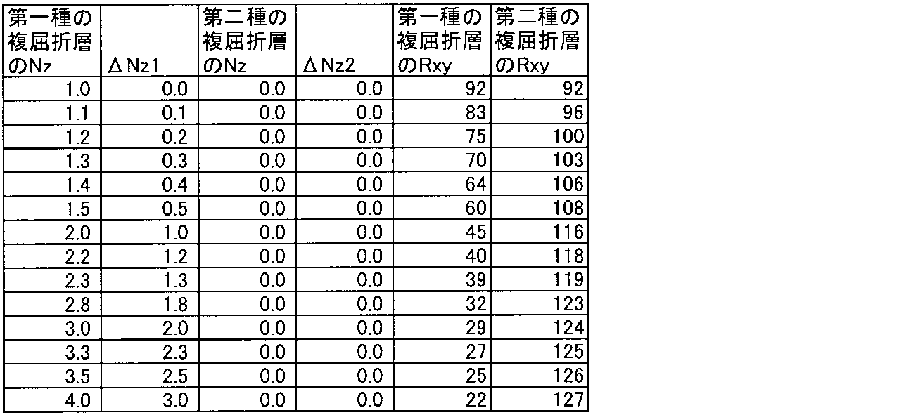
- the form of the liquid crystal display device of the present invention can be classified as follows from the difference in the degree of biaxiality between the first and second birefringent layers.
- the biaxial parameter ⁇ Nz1 of the first type birefringent layer is defined as
- the biaxial parameter ⁇ Nz2 of the second type birefringent layer is defined as
- the first type birefringent layer satisfies Nz> 0.9, and the second type birefringent layer satisfies Nz ⁇ 0.1. Therefore, the liquid crystal display device has ⁇ Nz1 ⁇ 0, and ⁇ Nz2 ⁇ 0 is satisfied.
- the form (a) is a form in which the first and second birefringent layers have the same degree of biaxiality. According to this aspect, the symmetry of the viewing angle characteristic is improved, and a liquid crystal display having a high contrast ratio in a wide viewing angle range can be realized.
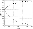
- the optimum Rxy was determined from the value at which the contrast ratio becomes the highest when the liquid crystal display device is observed from the direction that bisects the angle formed by the absorption axes of the first and second polarizers.
- the “in-plane slow axis of the birefringent layer” refers to the direction of the dielectric main axis (x-axis direction) corresponding to the main refractive index nx. Further, Rxz described later is the main refractive index in the in-plane direction of the birefringent layer (including the liquid crystal cell and the ⁇ / 4 plate) is nx, ny (nx ⁇ ny), and the main in the out-of-plane direction (thickness direction).
- the Rxy of the first and second birefringent layers is most preferably the optimum value shown in FIG. 3 and Table 1. As long as the contrast ratio at an oblique viewing angle is not lowered, it may be slightly deviated from the optimum value. From the viewpoint of sufficiently achieving the effects of the present invention, an optimal value in the range of ⁇ 15 nm is preferable.
- the first type birefringent layer Rxy and the second type birefringent layer are used. It can be said that Rxy is preferably in the range of 45 to 64 nm.
- the form (b) is a form in which the biaxial parameter of the first type birefringent layer is relatively small and the biaxial parameter of the second type birefringent layer is relatively large.
- the phase difference Rxy required for the first type birefringent layer can be reduced as compared with the above-described form (a), and therefore the first type birefringent layer has a retardation development property. Even in the case of a small material, a liquid crystal display with a high contrast ratio can be realized in a wide viewing angle range.
- the optimum Rxy was determined from the value at which the contrast ratio becomes the highest when the liquid crystal display device is observed from the direction that bisects the angle formed by the absorption axes of the first and second polarizers. From the viewpoint of realizing a liquid crystal display having a high contrast ratio in a wide viewing angle range, the Rxy of the first and second birefringent layers is most preferably the optimum value shown in FIG. 4 and Table 2.
- the contrast ratio at an oblique viewing angle is not lowered, it may be slightly deviated from the optimum value.
- an optimal value in the range of ⁇ 15 nm is preferable.
- the above (a) ( ⁇ Nz1 ⁇ Nz2). Therefore, with respect to the form (b), the optimum Rxy for ⁇ Nz1 and ⁇ Nz2 is considered to be between the optimum Rxy that can be read from Table 1 and the optimum Rxy that can be read from Table 2.
- the form (c) is a form in which the biaxial parameter of the first type birefringent layer is relatively large and the biaxial parameter of the second type birefringent layer is relatively small. According to this embodiment, the phase difference Rxy necessary for the second birefringent layer can be reduced as compared with the embodiment (a). Even in the case of a small material, a liquid crystal display with a high contrast ratio can be realized in a wide viewing angle range.
- the optimum Rxy was determined from the value at which the contrast ratio becomes the highest when the liquid crystal display device is observed from the direction that bisects the angle formed by the absorption axes of the first and second polarizers. From the viewpoint of realizing a liquid crystal display with a high contrast ratio in a wide viewing angle range, the Rxy of the first and second birefringent layers is most preferably the optimum value shown in FIG.
- the first birefringent layer preferably satisfies 2.0 ⁇ Nz ⁇ 4.0, and more preferably satisfies 2.3 ⁇ Nz ⁇ 3.3. According to this, a liquid crystal display device having a high contrast ratio in a wide viewing angle range can be realized at low cost. The reason is as follows.
- a linearly polarized VA mode optical compensation using a retardation film has been proposed to realize a high contrast ratio in a wide viewing angle range.
- a configuration using two biaxial retardation films has been put into practical use.
- of the liquid crystal cell, but is 2 for a typical VA mode liquid crystal cell retardation Rlc 290 to 370 nm.
- the phase difference condition of the first type birefringent layer and the second type birefringent layer is adjusted within a range where a high contrast ratio can be realized in a wide viewing angle range, and the first type birefringent layer is adjusted. If the same retardation condition as the biaxial retardation film put into practical use in the linearly polarized light VA mode can be selected as the refractive layer, it is preferable from the viewpoint of common use of members and cost reduction.
- the biaxial retardation film is generally used in large TV applications and the like, and can be easily obtained at low cost.
- the biaxial retardation film having the above retardation condition as the first type birefringent layer according to the present invention all right.
- the principle is explained using the Poincare sphere as follows.
- Poincare sphere The concept of Poincare sphere is widely known in the field of crystal optics and the like as a useful technique for tracking the polarization state changing through the birefringent layer (for example, Hiroshi Takasaki, “Crystal optics”, Morikita Publishing, 1975, p.146-163).
- right-handed polarized light is represented in the upper hemisphere
- left-handed polarized light is represented in the lower hemisphere
- linearly polarized light is represented in the equator
- right circularly polarized light and left circularly polarized light are represented in the upper and lower poles.
- the two polarization states that are symmetric with respect to the center of the sphere form a pair of orthogonal polarization because the absolute values of the ellipticity angles are equal and the polarities are opposite.
- the effect of the birefringent layer on the Poincare sphere is that the polarization state immediately before passing through the birefringent layer is expressed by the slow axis on the Poincare sphere (in other words, the polarization of the slow natural mode of the birefringent layer).
- the position of the point representing the state.) Is converted into a point rotated and rotated counterclockwise by an angle determined by (2 ⁇ ) ⁇ (phase difference) / (wavelength) (unit: rad) ( The same thing can be done by rotating clockwise around the fast axis.)
- the rotation center and the rotation angle when observed from an oblique direction are determined by the slow axis and the phase difference at the observation angle.
- the axis depends on the observation angle, the Nz coefficient defined by (nx ⁇ nz) / (nx ⁇ ny), or the biaxial parameters ⁇ Nz1 and ⁇ Nz2 defined above, and the phase difference when observed from an oblique direction is , Depending on the observation angle, biaxial parameters ⁇ Nz1, ⁇ Nz2, and phase differences Rxy and Rxz.
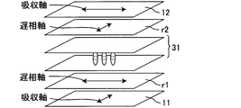
- the first polarizer (absorption axis orientation 90 °) 11 the first biaxial retardation film (slow axis orientation 0 °) r1, the VA mode liquid crystal cell 31, the second The biaxial retardation film (slow axis orientation 90 °) r2 and the second polarizer (absorption axis orientation 0 °) are laminated, and two biaxial retardation films are used.
- the first polarizer (absorption axis orientation 90 °) 11 the first biaxial retardation film (slow axis orientation 0 °) r1
- the VA mode liquid crystal cell 31 the second The biaxial retardation film (slow axis orientation 90 °) r2 and the second polarizer (absorption axis orientation 0 °) are laminated, and two biaxial retardation films are used.
- the polarization state immediately after the light emitted from the backlight (not shown; under the first polarizer 11) is transmitted through the first polarizer 11 is located at the point P0 on the Poincare sphere, and the point E
- the polarization state that can be absorbed by the second polarizer 12, that is, the extinction position (absorption axis direction) of the second polarizer 12 does not match. This is illustrated in FIG. 7A when illustrated on the S1-S2 plane of the Poincare sphere, and as illustrated in FIG. 7B when illustrated on the S1-S3 plane.
- the points representing the respective polarization states are actually on the Poincare sphere, they are projected onto the S1-S2 plane and the S1-S3 plane for illustration.
- the point P0 and the point E that should have overlapped on the S2 axis do not overlap when observed from an oblique direction of azimuth 45 ° and pole 60 °.
- the point P0 is reached.
- the existing polarization state undergoes rotational transformation at a specific angle around the slow axis of the first biaxial retardation film r1 represented by the point R1 on the Poincare sphere, and reaches the point P1.
- the rotation direction at this time is counterclockwise when viewed from the point R1 toward the origin O.
- the VA mode liquid crystal cell 31 it undergoes rotational conversion at a specific angle around the slow axis of the liquid crystal cell represented by the point LC on the Poincare sphere, and reaches the point P2.
- the rotation direction at this time is counterclockwise when viewed from the point LC toward the origin O. Since the point P2 is on the southern hemisphere of the Poincare sphere, in FIG.
- the point P2 and an arrow indicating movement to the point are indicated by a dotted line.
- the second biaxial retardation film r2 around the slow axis of the second biaxial retardation film r2 represented by the point R2 (slow axis) on the Poincare sphere.
- the rotation direction at this time is counterclockwise when viewed from the point R2 toward the origin O.
- FIG. 7B illustrated on the S1-S3 plane for the sake of illustration, the conversion from the point P2 to P3 is performed by the second two axes represented by the point R2 (fast axis) on the Poincare sphere.
- the liquid crystal display device of FIG. 6 can block light from the backlight even when observed from an azimuth 45 ° pole 60 °, similarly to the observation from the front direction. That is, the liquid crystal display device shown in FIG. 6 uses three birefringent media including a first biaxial retardation film r1, a VA mode liquid crystal cell 31, and a second biaxial retardation film r2. The polarization state represented by the point P0 is finally converted to the polarization state represented by the point E through the points P1 and P2.
- the VA mode liquid crystal cell 31 and the second biaxial retardation film r2 are removed, and instead of these, a biaxial retardation film r2 having a slow axis represented by a point R2 ′ on the Poincare sphere.
- a biaxial retardation film r2 having a slow axis represented by a point R2 ′ on the Poincare sphere Consider the case where 'is placed.
- the point P1 is not counterclockwise as viewed from the point R2 ′ toward the origin O around the slow axis of the biaxial retardation film r2 ′ represented by the point R2 ′ on the Poincare sphere. Since clockwise rotation conversion is performed, if an appropriate phase difference Rxy is selected, the converted point P2 ′ can be superimposed on the point E.
- the second kind of birefringence satisfying Nz ⁇ 0.1. It has been found that the layers may be arranged such that the in-plane slow axis forms an angle of 0 ° with the absorption axis of the second polarizer 12.
- the overall configuration in this case is shown in FIG. 8 includes a first polarizer (absorption axis orientation 90 °) 11, a first biaxial retardation film (slow axis orientation 0 °) r1, and a second biaxial retardation.
- the same retardation condition as that of the biaxial retardation film put into practical use in the linearly polarized VA mode can be selected as the first birefringent layer of the present invention.
- the biaxial parameter ⁇ Nz1 of the first type birefringent layer and the biaxial parameter ⁇ Nz2 of the second type birefringent layer are set.
- the phase difference Rxy of the second type birefringent layer is substantially the same as the phase difference Rxy of the first type birefringent layer. It is preferable.
- first birefringent layer first biaxial retardation film r1 in the above description
- second birefringent layer second biaxial retardation film r2 ′ in the above description
- a high contrast ratio can be obtained in a wide viewing angle range in a form that does not include other birefringent media between the first and second birefringent media.
- a second type of birefringent layer including a first ⁇ / 4 plate, a liquid crystal cell, and a second ⁇ / 4 plate.
- the influence of birefringence of these birefringent media can be minimized in the oblique direction, the same effect as when these birefringent media are not included can be obtained.
- the liquid crystal display device appropriately controls the Nz coefficient of the first and second ⁇ / 4 plates.
- the liquid crystal display device has Rxy ⁇ 10 nm between at least one of the first ⁇ / 4 plate and the liquid crystal cell and between the liquid crystal cell and the second ⁇ / 4 plate and It is preferable to have a third type birefringent layer that satisfies Rxz> 0 nm.
- Rxz 0 nm
- the third birefringent layer is preferably disposed adjacent to the liquid crystal cell.
- adjacent arrangement means that no birefringent medium is provided between the liquid crystal cell and the third type birefringent layer.
- the third type birefringent layer and the liquid crystal cell A form in which an isotropic film is disposed between the two is also included.
- the optimum retardation Rxz of the third type birefringent layer (in the case of having a plurality of third type birefringent layers means the sum of the respective Rxz) is Nz of the first ⁇ / 4 plate.
- the coefficient is defined as Nzq1
- the Nz coefficient of the second ⁇ / 4 plate is defined as Nzq2
- the phase difference Rlc of the liquid crystal cell is defined as
- (Nzq1 + Nzq2) is large, the optimum value of Rxz can be zero, which means that the third type birefringent layer is unnecessary.
- Rxz Rlc ⁇ 137.5 ⁇ (Nzq1 + Nzq2-1) (2)
- Rxz of the third birefringent layer is an optimum value satisfying the above formula (2), but contrast at an oblique viewing angle. As long as the ratio does not decrease, it may deviate somewhat from the optimum value. From the viewpoint of sufficiently achieving the effects of the present invention, an optimal value in the range of ⁇ 50 nm is preferable.
- the basis for calculating the optimum phase difference Rxz is as follows.
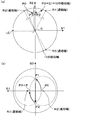
- a first polarizer (absorption axis orientation 90 °) 11 a first kind of birefringent layer (slow axis orientation 0 °) r1, a first ⁇ / 4 plate (slow axis orientation) 135 °) q1, VA mode liquid crystal cell 31, third type birefringent layer r3, second ⁇ / 4 plate (slow axis direction 45 °) q2, second type birefringent layer (slow axis direction 0) °)
- a liquid crystal display device configured by sequentially laminating r2 and a second polarizer (absorption axis azimuth 0 °) 12 is observed from an oblique direction of azimuth 45 ° and pole 60 °.
- the slow axis Q1 of the first ⁇ / 4 plate q1 When observed from the oblique direction, on the Poincare sphere, the slow axis Q1 of the first ⁇ / 4 plate q1, the slow axis LC of the VA mode liquid crystal cell 31, and the slow axis R3 of the third birefringent layer r3.
- the slow axis Q2 of the second ⁇ / 4 plate q2 is in a positional relationship as shown in FIG.
- the rotation angle is effective for each of the first ⁇ / 4 plate q1, the VA mode liquid crystal cell 31, the third birefringent layer r3, and the second ⁇ / 4 plate q2 when observed from the oblique direction.
- the light emitted from the backlight passes through the first polarizer 11 and the first type birefringent layer r1 in this order, and on the Poincare sphere.
- the light After reaching the polarization state represented by the point P1, the light passes through the first ⁇ / 4 plate q1 and passes through the VA mode liquid crystal cell 31 and is represented by the point P3.
- the polarization state is sequentially converted to the polarization state represented by the point P4 through the third birefringent layer r3, the polarization state represented by the point P5 through the second ⁇ / 4 plate q2, and finally A point P5 representing a typical polarization state overlaps with the point P1, and does not move at all from the state before entering the first ⁇ / 4 plate q1.
- the liquid crystal display device of FIG. 10 is optically equivalent to the laminate of FIG. 8 and has a high contrast ratio in observation from an oblique direction of at least 45 ° azimuth and 60 ° pole.
- the optimum phase difference Rxz of the third birefringent layer is derived.
- Expression (2) is obtained by substituting Expressions (3) to (6) into Expression (7) and rearranging them.
- Rlc 320 nm
- the position of each point is roughly shown, and some are not strictly accurate.
- the arrows representing the trajectories are not shown for the conversion of the points P2 to P5.
- the liquid crystal display device is observed from an oblique direction with an azimuth of 0 ° and a pole of 60 °.
- the slow axis Q1 of the first ⁇ / 4 plate q1 When observed from the oblique direction, on the Poincare sphere, the slow axis Q1 of the first ⁇ / 4 plate q1, the slow axis LC of the VA mode liquid crystal cell 31, and the slow axis R3 of the third birefringent layer r3.
- the slow axis Q2 of the second ⁇ / 4 plate q2 is in a positional relationship as shown in FIG.
- the rotation center of the conversion by the VA mode liquid crystal cell 31 and the rotation center of the conversion by the third type birefringent layer r3 coincide with each other, the rotation center of the conversion by the first ⁇ / 4 plate q1 and the second ⁇ / The rotation center of conversion by the four plates q2 does not coincide with the previous two.
- the light emitted from the backlight passes through the first polarizer 11 and the first type birefringent layer r1 in order, and is observed from a point P1 on the Poincare sphere (azimuth 0 °, pole 60 ° from an oblique direction).
- a point P1 on the Poincare sphere azimuth 0 °, pole 60 ° from an oblique direction.
- the point P1 overlaps the point P0 because it is not affected by the first type birefringent layer r1, and then the first ⁇ / 4 plate q1 is moved to the polarization state represented by Passing through the VA mode liquid crystal cell 31 to the polarization state represented by the point P2, passing through the VA mode liquid crystal cell 31, passing through the third birefringent layer r3 and passing through the third birefringent layer r3 into the polarization state represented by the point P4. Then, the light passes through the second ⁇ / 4 plate q2 and is sequentially converted into the polarization state represented by the point P5, and the point P5 representing the final polarization state does not necessarily overlap the point P1.
- the liquid crystal display device of FIG. 10 is not necessarily optically equivalent to the laminate of FIG. 8, and a sufficiently high contrast ratio may not be obtained.
- the liquid crystal display device of the present invention has a high contrast ratio even when observed from an oblique direction with an azimuth of 0 ° and a pole of 60 °, and from the viewpoint of realizing a liquid crystal display with a high contrast ratio in a wide viewing angle range.
- the slow axis Q1 of the first ⁇ / 4 plate q1 and the slow axis Q2 of the second ⁇ / 4 plate q2 on the Poincare sphere are always the origin regardless of the observation direction.
- the position is symmetrical with respect to O.
- the phase difference ⁇ q2 ( ⁇ , 60) is substantially equal to each other with respect to an arbitrary direction ⁇ .
- the conversion by the VA mode liquid crystal cell 31 and the conversion by the birefringent layer r3 have the same rotation center and the same rotation angle, and the rotation angles are opposite to each other.
- the conversion by the first ⁇ / 4 plate q1 and the conversion by the second ⁇ / 4 plate q2 have the same rotation center and the same rotation angle, and the rotation angles are opposite to each other.
- the light emitted from the backlight passes through the first polarizer 11 and the first type birefringent layer r1 in order, and is observed from a point P1 on the Poincare sphere (azimuth 0 °, pole 60 ° from an oblique direction).
- azimuth 0 °, pole 60 ° from an oblique direction In FIG.
- the point P1 overlaps the point P0 because it is not affected by the first type birefringent layer r1, and then the first ⁇ / 4 plate q1 is moved to the polarization state represented by Passing through the VA mode liquid crystal cell 31 to the polarization state represented by the point P2, passing through the VA mode liquid crystal cell 31, passing through the third birefringent layer r3 and passing through the third birefringent layer r3 into the polarization state represented by the point P4. Then, the light passes through the second ⁇ / 4 plate q2 and is sequentially converted to the polarization state represented by the point P5, and the point P5 representing the final polarization state overlaps the point P1 and enters the first ⁇ / 4 plate q1.
- the position of each point is roughly shown, and some are not strictly accurate.
- the first birefringent layer is disposed on one side of the liquid crystal cell, and the second birefringent layer is disposed on the other side of the liquid crystal cell.
- the first polarizer can be protected by the first type birefringent layer
- the second polarizer can be protected by the second type birefringent layer.
- it is not necessary to dispose a TAC film, an isotropic film or the like as a protective film for the polarizer it is not necessary to dispose a TAC film, an isotropic film or the like as a protective film for the polarizer, and the liquid crystal display device can be made thinner and the cost can be reduced.
- using the ⁇ / 4 plate as a protective film for the polarizer is difficult in terms of manufacturing such as roll-to-roll bonding cannot be used to make the absorption axis direction 45 °. .
- the polarizer, the first type birefringent layer and the second type birefringent layer are rolled.
- two-roll bonding it is necessary to longitudinally stretch one of the birefringent layers so that the axis is oriented in the roll longitudinal direction. In this case, it is difficult to effectively use the birefringent layer that is widely used in large TVs.
- the first type birefringent layer satisfying Nz> 0.9 and the second type birefringent layer satisfying Nz ⁇ 0.1 are used in combination, thereby reducing the cost.
- it can be easily manufactured, and a high contrast ratio can be realized in a wide viewing angle range.
- Such a liquid crystal display device of the present invention can be suitably used for display devices such as televisions and mobile devices.
- the birefringent layer used in the present invention is not particularly limited in terms of materials and optical performance, and includes, for example, a stretched polymer film, a fixed liquid crystal material orientation, a thin plate composed of an inorganic material, and the like. Can be used.
- the method for forming the birefringent layer is not particularly limited.
- a solvent casting method, a melt extrusion method, or the like can be used.
- a method of simultaneously forming a plurality of birefringent layers by a coextrusion method may be used. As long as the desired phase difference is expressed, it may be unstretched or may be stretched.
- the stretching method is not particularly limited, and other specific stretching is performed under the action of the shrinkage force of the heat-shrinkable film, in addition to the roll-to-roll tensile stretching method, the inter-roll compression stretching method, the tenter transverse uniaxial stretching method, the longitudinal and transverse biaxial stretching method. The law etc. can be used.
- a method of applying a liquid crystalline material on a substrate film subjected to an alignment treatment and fixing the alignment can be used.
- a method that does not fix the alignment of the liquid crystal material may be used.
- a formation method similar to that for the liquid crystalline material may be used.
- first birefringent layer As the first kind of birefringent layer, a film obtained by stretching a film containing a material having a positive intrinsic birefringence as a component can be appropriately used. As described above, the first type birefringent layer may be a laminate of two or more birefringent layers. However, from the viewpoint of easy and low cost production, a single layer (single layer) It is preferably formed from a film.
- the material having a positive intrinsic birefringence include polycarbonate, polysulfone, polyethersulfone, polyethylene terephthalate, polyethylene, polyvinyl alcohol, norbornene, triacetylcellulose, and diacylcellulose.
- the second kind of birefringent layer is a stretched film containing a material having a negative intrinsic birefringence as a component, and a film containing a material having a positive intrinsic birefringence as a component is acting on the shrinkage force of the heat-shrinkable film. What extended
- stretched and processed below can be used suitably.
- a film obtained by stretching a film containing a material having a negative intrinsic birefringence as a component is preferable.
- the second birefringent layer may be a laminate of two or more birefringent layers.
- a single layer It is preferably formed from a film.
- the material having a negative intrinsic birefringence include polystyrene, polyvinyl naphthalene, polyvinyl biphenyl, polyvinyl pyridine, polymethyl methacrylate, polymethyl acrylate, N-substituted maleimide copolymer, polycarbonate having a fluorene skeleton, and triacetyl cellulose (particularly acetyl). And the like).
- the third type of birefringent layer a film obtained by stretching a film containing a material having a positive intrinsic birefringence as a component, a liquid crystal material such as cholesteric (chiral nematic) liquid crystal or discotic liquid crystal, polyimide, What applied the non-liquid crystalline material containing polyamide etc. can be used suitably.
- the third birefringent layer may be a laminate of two or more birefringent layers.
- a single layer single layer It is preferably formed from a film.
- first and second ⁇ / 4 plates About the 1st and 2nd (lambda) / 4 board, the thing similar to a 1st type, a 2nd type, and a 3rd type birefringent layer can be used suitably.
- the first and second ⁇ / 4 plates may be laminated with two or more birefringent layers.
- a single layer single layer It is preferably formed from a film.
- Polarizer for example, a material obtained by adsorbing and orienting an anisotropic material such as an iodine complex having dichroism on a polyvinyl alcohol (PVA) film can be appropriately used.
- PVA polyvinyl alcohol
- the liquid crystal cell only needs to perform black display by aligning liquid crystal molecules in the liquid crystal cell perpendicularly to the substrate surface, and examples of the display mode of such a liquid crystal cell include a VA mode. It is done.
- the VA mode includes an MVA mode, a CPA mode, a PVA mode, a BVA mode, a Reverse TN mode, and the like.
- the liquid crystal cell may be driven by a simple matrix method (passive matrix method), a plasma address method, or the like.
- a configuration of the liquid crystal cell for example, a liquid crystal is sandwiched between a pair of substrates on which electrodes are formed, and a display is performed by applying a voltage between the electrodes.
- FIG. 14 is a perspective view schematically showing the configuration of the liquid crystal display device of Example 1.
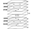
- the liquid crystal display device of Example 1 according to the present invention includes a TAC film 101, a first polarizer 111, a first type birefringent layer 151, a first ⁇ / 4 plate 181, and a VA. It is obtained by laminating the mode liquid crystal cell 131, the third birefringent layer 171, the second ⁇ / 4 plate 182, the second birefringent layer 161, the second polarizer 112, and the TAC film 102 in this order.
- VA mode liquid crystal display device is obtained by laminating the mode liquid crystal cell 131, the third birefringent layer 171, the second ⁇ / 4 plate 182, the second birefringent layer 161, the second polarizer 112, and the TAC film 102 in this order.
- VA mode liquid crystal display device is obtained by laminating the mode liquid crystal cell 131, the third birefringent layer 171, the second ⁇ /
- Table 4 shows the optical characteristics and axis settings of the various birefringent layers 151, 161, 171, ⁇ / 4 plates 181, 182, polarizers 111, 112, and liquid crystal cell 131 of this example. It should be noted that the TAC films 101 and 102 outside the polarizers 111 and 112 (the side closer to the liquid crystal cell 131 is defined as the inner side and the far side is defined as the outer side) affect the performance of the liquid crystal display device as long as it is transparent. In Table 4, the description of the optical characteristics is omitted. The same applies to each of the following examples, comparative examples, and reference examples.
- the axes of the birefringent layers 151, 161, 171 and the ⁇ / 4 plates 181, 182 are defined by the azimuth angle of the in-plane slow axis, and the axes of the polarizers 111, 112 are defined by the azimuth angle of the absorption axis. It is.
- the material names of the birefringent layers 151, 161, and 171 are indicated using the following abbreviations.
- NB Norbornene
- PC Polycarbonate
- PMMA Polymethyl methacrylate NM: N-substituted maleimide copolymer
- ChLC Cholesteric liquid crystal
- PI Polyimide TAC: Triacetyl cellulose Z: Isotropic film
- Examples 2 to 3 The liquid crystal display devices of Examples 2 to 3 according to the present invention are the same as Example 1 except that the phase difference Rxy and Nz coefficient of the first and second birefringent layers 151 and 161 are changed.
- Liquid crystal display device. Table 4 shows the optical characteristics and axis settings of the various birefringent layers 151, 161, 171, ⁇ / 4 plates 181, 182, polarizers 111, 112, and liquid crystal cell 131 of this example.
- Example 4 The liquid crystal display device of Example 4 according to the present invention is the same as the liquid crystal display device of Example 1 except that the Nz coefficients of the first and second ⁇ / 4 plates 181 and 182 are changed.
- Table 4 shows the optical characteristics and axis settings of the various birefringent layers 151, 161, 171, ⁇ / 4 plates 181, 182, polarizers 111, 112, and liquid crystal cell 131 of this example.
- Example 5 The liquid crystal display device of Example 5 according to the present invention is the same as the liquid crystal display device of Example 1 except that the material of the second birefringent layer 161 is changed.
- Table 4 shows the optical characteristics and axis settings of the various birefringent layers 151, 161, 171, ⁇ / 4 plates 181, 182, polarizers 111, 112, and liquid crystal cell 131 of this example.
- Example 6 to 7 The liquid crystal display devices of Examples 6 to 7 according to the present invention are the same as those of Example 1 except that the material of the third birefringent layer 171 is changed.
- Table 4 shows the optical characteristics and axis settings of the various birefringent layers 151, 161, 171, ⁇ / 4 plates 181, 182, polarizers 111, 112, and liquid crystal cell 131 of this example.
- FIG. 15 is a perspective view schematically illustrating the configuration of the liquid crystal display device according to the eighth embodiment.
- the phase difference Rxz and Nz coefficient of the first and second ⁇ / 4 plates 181 and 182 were changed, and the third-type birefringent layer 171 was omitted. Except for this, the liquid crystal display device is the same as that of the first embodiment.
- the optical characteristics and axis settings of the various birefringent layers 151 and 161, the ⁇ / 4 plates 181 and 182, the polarizers 111 and 112, and the liquid crystal cell 131 of this example are as shown in Table 5.
- Example 9 In the liquid crystal display device of Example 9 according to the present invention, the phase difference Rxz and the Nz coefficient of the second ⁇ / 4 plate 182 were changed to less than 0, and the phase difference Rxz of the third birefringent layer 171 was changed. Except for the change, the liquid crystal display device is the same as that of the first embodiment.
- the optical characteristics and axis settings of the various birefringent layers 151, 161, 171, ⁇ / 4 plates 181, 182, polarizers 111, 112, and liquid crystal cell 131 of this example are as shown in Table 6.
- Example 10 The liquid crystal display device of Example 10 according to the present invention is the same as that of Example 9 except that the materials of the second birefringent layer 161 and the second ⁇ / 4 plate 182 are changed. It is.
- the optical characteristics and axis settings of the various birefringent layers 151, 161, 171, ⁇ / 4 plates 181, 182, polarizers 111, 112, and liquid crystal cell 131 of this example are as shown in Table 6.
- Example 11 The liquid crystal display device of Example 11 according to the present invention is the same as the liquid crystal display device of Example 9 except that the material of the third birefringent layer 171 is changed.
- the optical characteristics and axis settings of the various birefringent layers 151, 161, 171, ⁇ / 4 plates 181, 182, polarizers 111, 112, and liquid crystal cell 131 of this example are as shown in Table 6.
- FIG. 16 is a perspective view schematically showing the configuration of the liquid crystal display device of Example 12.
- the third birefringent layer 171 is divided into two layers, and the first third birefringent layer 172 is disposed on one side of the liquid crystal cell.
- the liquid crystal display device is the same as that of Example 7 except that the second third-type birefringent layer 173 is disposed on the other side.
- Table 7 shows optical characteristics and axis settings of the various birefringent layers 151, 161, 172, 173, ⁇ / 4 plates 181, 182, polarizers 111, 112, and liquid crystal cell 131 of this example.
- FIG. 17 is a perspective view schematically showing the configuration of the liquid crystal display device of Example 13.
- the third birefringent layer 171 is divided into two layers, and the first third birefringent layer 174 is disposed on one side of the liquid crystal cell.
- the liquid crystal display device is the same as that of Example 11 except that the second third-type birefringent layer 175 is disposed on the other side.
- Table 7 shows optical characteristics and axis settings of various birefringent layers 151, 161, 174, 175, ⁇ / 4 plates 181, 182, polarizers 111, 112, and liquid crystal cell 131 of this example.
- FIG. 18 is a perspective view schematically showing the configuration of the liquid crystal display device of Comparative Example 1.
- the liquid crystal display device of Comparative Example 1 includes a TAC film 103, a first polarizer 113, a TAC film 105, a first ⁇ / 4 plate 183, a VA mode liquid crystal cell 132, and a second ⁇ . / 4 plate 184, TAC film 106, second polarizer 114, and TAC film 104 are laminated in this order to obtain a VA mode liquid crystal display device.
- the optical characteristics and axis settings of the TAC films 105 and 106, ⁇ / 4 plates 183 and 184, polarizers 113 and 114, and liquid crystal cell 132 of this comparative example are as shown in Table 8.
- the ⁇ / 4 plates 183 and 184 of this comparative example satisfy the relationship of nx>ny> nz.
- the absorption axis of the first polarizer 113 was set to 90 °, the left-right symmetry of the viewing angle was not obtained, so the absorption axis was reset to 70 °. .
- the cause of this asymmetry is considered to be because the viewing angle dependence of the circular birefringence (optical rotation) of the birefringent medium between the first polarizer 113 and the second polarizer 114 is large.
- FIG. 19 is a perspective view schematically showing the configuration of the liquid crystal display device of Comparative Example 2. 19, the TAC film 103, the first polarizer 115, the TAC film 105, the first ⁇ / 4 plate 185, the VA mode liquid crystal cell 132, the third type, This is a VA mode liquid crystal display device obtained by laminating the birefringent layer 176, the second ⁇ / 4 plate 186, the TAC film 106, the second polarizer 116, and the TAC film 104 in this order.
- the optical properties and axis settings of the TAC films 105 and 106, ⁇ / 4 plates 185 and 186, polarizers 115 and 116, and liquid crystal cell 132 of this comparative example are as shown in Table 8.
- the ⁇ / 4 plates 185 and 186 of this comparative example satisfy the relationship of nx>nz> ny.
- FIG. 20 is a perspective view schematically showing the configuration of the liquid crystal display device of Comparative Example 3.
- the liquid crystal display device of Comparative Example 3 includes a TAC film 103, a first polarizer 115, an isotropic film 191, a ⁇ / 2 plate (HWP) 201, and a first ⁇ / 4 plate 187.
- the VA mode liquid crystal cell 132, the third birefringent layer 177, the second ⁇ / 4 plate 188, the isotropic film 192, the second polarizer 116, and the TAC film 104 were obtained in this order. It is a VA mode liquid crystal display device.
- the optical characteristics and axis settings of the third birefringent layer 177, ⁇ / 2 plate 201, ⁇ / 4 plates 187 and 188, polarizers 115 and 116, and liquid crystal cell 132 of this comparative example are as shown in Table 8. is there.
- the ⁇ / 4 plates 187 and 188 and the ⁇ / 2 plate 201 of this comparative example satisfy the relationship of nx>nz> ny.
- FIG. 21 is a perspective view schematically showing the configuration of the liquid crystal display device of Comparative Example 4.
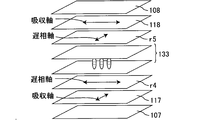
- the liquid crystal display device of Comparative Example 4 includes a TAC film 107, a first polarizer 117, a first biaxial retardation film r4, a VA mode liquid crystal cell 133, and a second biaxial property.
- This is a VA mode liquid crystal display device obtained by laminating the retardation film r5, the second polarizer 118, and the TAC film 108 in this order.
- the optical characteristics and axis settings of the biaxial retardation films r4 and r5, polarizers 117 and 118, and the liquid crystal cell 133 of this comparative example are as shown in Table 9.
- the liquid crystal display device of this comparative example is a linearly polarized VA mode liquid crystal display device.
- Comparative Examples 5 to 6 The liquid crystal display devices of Comparative Examples 5 to 6 are the same as those of Comparative Example 4 except that the retardation Rxy and Nz coefficient of the biaxial retardation films r4 and r5 and the Rlc of the liquid crystal cell were changed. It is a display device.
- the optical characteristics and axis settings of the biaxial retardation films r4 and r5, polarizers 117 and 118, and the liquid crystal cell 133 of this comparative example are as shown in Table 9.
- the contrast viewing angles of the liquid crystal display devices of each example were measured, and CR (45, 60) and CR (0, 60) were arranged in Tables 4 to 9 below.
- the CR (45, 60) of the liquid crystal display devices of Examples 1 to 13 according to the present invention was higher than the CR (45, 60) of Comparative Examples 1 and 2, and in the visual evaluation, Comparative Examples 1 to 2 had a contrast viewing angle better than 2.
- the liquid crystal display device of Comparative Example 3 has an excellent contrast viewing angle, but uses three biaxial retardation films that are difficult to manufacture and controlled to nx>nz> ny. Further, the liquid crystal display devices of Comparative Examples 4 to 6 had excellent contrast viewing angles, but because of the linearly polarized VA mode, the liquid crystal display devices of Examples 1 to 13 according to the present invention have a white display luminance. It was about 15% lower than that.
- FIG. 1 shows the axial relationship of a birefringent layer and a polarizer when the optical axis of a polarizer and the optical axis of a birefringent layer are arrange
- positioned orthogonally seeing from a front direction (a) is a front direction. 2 shows the axial relationship between the birefringent layer and the polarizer when observed from the above, and (b) shows the axial relationship between the birefringent layer and the polarizer when observed from an oblique direction.
- FIG. 1 shows the axial relationship of a birefringent layer and a polarizer when the optical axis of a polarizer and the optical axis of a birefringent layer are arrange
- positioned orthogonally seeing from a front direction (a) is a front direction. 2 shows the axial relationship between the birefringent layer and the polarizer when observed from the above, and (b) shows the axial relationship between the birefringent layer and the polarizer
- FIG. 6 is a diagram showing a relationship
- FIG. 7 is a diagram showing a change in polarization state on the Poincare sphere in the liquid crystal display device of FIG.
- FIG. 6 is a diagram in which the polarization state is projected onto the S1-S2 plane, and (b) is a diagram showing the polarization state. It is the figure projected on the S1-S3 plane. It is the figure which showed typically the laminated body which optically compensated the orthogonality of the 1st and 2nd polarizer using two biaxial phase difference films in the observation from azimuth
- FIG. 9 is a diagram showing a change in the polarization state in the laminate of FIG. 8 on a Poincare sphere, (a) is a diagram in which the polarization state is projected onto the S1-S2 plane, and (b) is a diagram illustrating the polarization state in S1.
- FIG. 1 is a diagram schematically illustrating a configuration of a liquid crystal display device of Example 1.
- FIG. FIG. 10 is a diagram schematically showing a configuration of a liquid crystal display device of Example 8.
- FIG. 1 is a diagram schematically illustrating a configuration of a liquid crystal display device of Example 1.
- FIG. FIG. 10 is a diagram schematically showing a configuration of a liquid crystal display device of Example 8.
- FIG. 1 is a diagram schematically illustrating a
- 16 is a diagram schematically showing a configuration of a liquid crystal display device of Example 12. It is a figure which shows typically the structure of the liquid crystal display device of Example 13. It is a figure which shows typically the structure of the liquid crystal display device of the comparative example 1. It is a figure which shows typically the structure of the liquid crystal display device of the comparative example 2. It is a figure which shows typically the structure of the liquid crystal display device of the comparative example 3. It is a figure which shows typically the structure of the liquid crystal display device of the comparative example 4.
Landscapes
- Physics & Mathematics (AREA)
- General Physics & Mathematics (AREA)
- Optics & Photonics (AREA)
- Nonlinear Science (AREA)
- Mathematical Physics (AREA)
- Chemical & Material Sciences (AREA)
- Crystallography & Structural Chemistry (AREA)
- Polarising Elements (AREA)
- Liquid Crystal (AREA)
Abstract
Description
(A)nx>ny>nzの関係を満たすλ/4板を用いる方法
(B)nx>nz>nyの関係を満たすλ/4板とnx=ny>nzの関係を満たす位相差フィルム(いわゆるネガティブCプレート)を組み合わせて用いる方法
(C)(B)の構成に加えて、nx>nz>nyの関係を満たすλ/2板を1枚又は2枚組み合わせて用いる方法
以下に本発明を詳述する。
Rxy=(72-9.6×ΔNz1) (1)


Rxz=Rlc-137.5×(Nzq1+Nzq2-1) (2)
Γq1(45、60)=140+56.1×(Nzq1-0.5) (3)
Γlc(45、60)=0.408×Rlc (4)
Γr3(45、60)=0.408×Rxz (5)
Γq2(45、60)=140-56.1×(Nzq2-0.5) (6)
+Γq1(45、60)-Γlc(45、60)+Γr3(45、60)-Γq2(45、60)=0 (7)
本発明に用いられる複屈折層としては、材料や光学的性能について特に限定されず、例えば、ポリマーフィルムを延伸したもの、液晶性材料の配向を固定したもの、無機材料から構成される薄板等を用いることができる。
第一種の複屈折層としては、固有複屈折が正の材料を成分として含むフィルムを延伸加工したもの等を適宜用いることができる。このように、第一種の複屈折層は、2層以上の複屈折層が積層されたものであってもよいが、容易、かつ低コストに作製する観点からは、単層(単一のフィルムから形成されたもの)であることが好ましい。固有複屈折が正の材料としては、例えば、ポリカーボネート、ポリサルフォン、ポリエーテルサルフォン、ポリエチレンテレフタレート、ポリエチレン、ポリビニルアルコール、ノルボルネン、トリアセチルセルロース、ジアチルセルロース等が挙げられる。
第二種の複屈折層としては、固有複屈折が負の材料を成分として含むフィルムを延伸加工したもの、固有複屈折が正の材料を成分として含むフィルムを熱収縮性フィルムの収縮力の作用下で延伸加工したもの等を適宜用いることができる。なかでも、製造方法の簡便化の観点からは、固有複屈折が負の材料を成分として含むフィルムを延伸加工したものが好ましい。このように、第二種の複屈折層は、2層以上の複屈折層が積層されたものであってもよいが、容易、かつ低コストに作製する観点からは、単層(単一のフィルムから形成されたもの)であることが好ましい。固有複屈折が負の材料としては、例えば、ポリスチレン、ポリビニルナフタレン、ポリビニルビフェニル、ポリビニルピリジン、ポリメチルメタクリレート、ポリメチルアクリレート、N置換マレイミド共重合体、フルオレン骨格を有するポリカーボネート、トリアセチルセルロース(特にアセチル化度の小さいもの)等が挙げられる。
第三種の複屈折層としては、固有複屈折が正の材料を成分として含むフィルムを延伸加工したもの、コレステリック(カイラルネマチック)液晶やディスコチック液晶等の液晶性材料を塗布したもの、ポリイミドやポリアミド等を含む非液晶性材料を塗布したもの等を適宜用いることができる。このように、第三種の複屈折層は、2層以上の複屈折層が積層されたものであってもよいが、容易、かつ低コストに作製する観点からは、単層(単一のフィルムから形成されたもの)であることが好ましい。
第一及び第二のλ/4板については、第一種、第二種及び第三種の複屈折層と同様のものを適宜用いることができる。第一及び第二のλ/4板についても、2層以上の複屈折層が積層されたものであってもよいが、容易、かつ低コストに作製する観点からは、単層(単一のフィルムから形成されたもの)であることが好ましい。
偏光子としては、例えば、ポリビニルアルコール(PVA)フィルムに二色性を有するヨウ素錯体等の異方性材料を吸着配向させたもの等を適宜用いることができる。
液晶セルとしては、液晶セル中の液晶分子を基板面に垂直に配向させることで黒表示を行うものでさえあればよく、そのような液晶セルの表示モードとしては、例えば、VAモード等が挙げられる。VAモードには、MVAモード、CPAモード、PVAモード、BVAモード、ReverseTNモード等が含まれる。また、液晶セルの駆動形式としては、TFT方式(アクティブマトリクス方式)のほか、単純マトリクス方式(パッシブマトリクス方式)、プラズマアドレス方式等であってもよい。液晶セルの構成としては、例えば、それぞれに電極が形成された一対の基板間に液晶を狭持し、それぞれの電極間に電圧を印加することで表示を行うものが挙げられる。
デュアル・リターダー・ローテート方式のポーラリメータ(Axometrics社製、商品名:Axo-scan)を用いて測定した。Rxyは複屈折層の法線方向から実測した。nx、ny、nz、Rxz及びNzは、複屈折層の法線方向、法線方向から-50°~50°傾斜した各斜め方向から位相差を測定し、公知の屈折率楕円体式のカーブフィッティングにより算出した。傾斜方位は面内遅相軸と直交する方位とした。また、nx、ny、nz、Rxz及びNzは、カーブフィッティングの計算条件として与える平均屈折率=(nx+ny+nz)/3に依存するが、各複屈折層の平均屈折率を1.5に統一して計算した。実際の平均屈折率が1.5と異なる複屈折層についても平均屈折率1.5を想定して換算した。
視野角測定装置(ELDIM社製、商品名:EZContrast160)を用いて測定した。光源にはシャープ社製液晶テレビ(商品名:LC37-GH1)搭載のバックライトを用いた。方位45°、極60°の斜め方向における白表示と黒表示の輝度を測定し、その比をCR(45、60)とした。また、方位0°、極60°の斜め方向における白表示と黒表示の輝度を測定し、その比をCR(0、60)とした。
図14は、実施例1の液晶表示装置の構成を模式的に示す斜視図である。
本発明に係る実施例1の液晶表示装置は、図14に示すように、TACフィルム101、第一の偏光子111、第一種の複屈折層151、第一のλ/4板181、VAモード液晶セル131、第三種の複屈折層171、第二のλ/4板182、第二種の複屈折層161、第二の偏光子112、TACフィルム102をこの順に積層して得られたVAモードの液晶表示装置である。
NB:ノルボルネン
PC:ポリカーボネート
PMMA:ポリメチルメタクリレート
NM:N置換マレイミド共重合体
ChLC:コレステリック液晶
PI:ポリイミド
TAC:トリアセチルセルロース
Z:等方性フィルム
本発明に係る実施例2~3の液晶表示装置は、第一種及び第二種の複屈折層151、161の位相差Rxy及びNz係数を変更したことを除いては、実施例1と同様の液晶表示装置である。本実施例の各種複屈折層151、161、171、λ/4板181、182、偏光子111、112、液晶セル131の光学特性及び軸設定については表4に示す通りである。
本発明に係る実施例4の液晶表示装置は、第一及び第二のλ/4板181、182のNz係数を変更したことを除いては、実施例1と同様の液晶表示装置である。本実施例の各種複屈折層151、161、171、λ/4板181、182、偏光子111、112、液晶セル131の光学特性及び軸設定については表4に示す通りである。
本発明に係る実施例5の液晶表示装置は、第二種の複屈折層161の材料を変更したことを除いては、実施例1と同様の液晶表示装置である。本実施例の各種複屈折層151、161、171、λ/4板181、182、偏光子111、112、液晶セル131の光学特性及び軸設定については表4に示す通りである。
本発明に係る実施例6~7の液晶表示装置は、第三種の複屈折層171の材料を変更したことを除いては、実施例1と同様の液晶表示装置である。本実施例の各種複屈折層151、161、171、λ/4板181、182、偏光子111、112、液晶セル131の光学特性及び軸設定については表4に示す通りである。
図15は、実施例8の液晶表示装置の構成を模式的に示す斜視図である。
本発明に係る実施例8の液晶表示装置は、第一及び第二のλ/4板181、182の位相差Rxz及びNz係数を変更したことと、第三種の複屈折層171を省いたことを除いては、実施例1と同様の液晶表示装置である。本実施例の各種複屈折層151、161、λ/4板181、182、偏光子111、112、液晶セル131の光学特性及び軸設定については表5に示す通りである。
本発明に係る実施例9の液晶表示装置は、第二のλ/4板182の位相差Rxz及びNz係数を0未満に変更したことと、第三種の複屈折層171の位相差Rxzを変更したことを除いては、実施例1と同様の液晶表示装置である。本実施例の各種複屈折層151、161、171、λ/4板181、182、偏光子111、112、液晶セル131の光学特性及び軸設定については表6に示す通りである。
本発明に係る実施例10の液晶表示装置は、第二種の複屈折層161及び第二のλ/4板182の材料を変更したことを除いては、実施例9と同様の液晶表示装置である。本実施例の各種複屈折層151、161、171、λ/4板181、182、偏光子111、112、液晶セル131の光学特性及び軸設定については表6に示す通りである。
本発明に係る実施例11の液晶表示装置は、第三種の複屈折層171の材料を変更したことを除いては、実施例9と同様の液晶表示装置である。本実施例の各種複屈折層151、161、171、λ/4板181、182、偏光子111、112、液晶セル131の光学特性及び軸設定については表6に示す通りである。
図16は、実施例12の液晶表示装置の構成を模式的に示す斜視図である。本発明に係る実施例12の液晶表示装置は、第三種の複屈折層171を2層に分割し、液晶セルの一方の側に第一の第三種の複屈折層172を配置し、他方の側に第二の第三種の複屈折層173を配置したことを除いては、実施例7と同様の液晶表示装置である。本実施例の各種複屈折層151、161、172、173、λ/4板181、182、偏光子111、112、液晶セル131の光学特性及び軸設定については表7に示す通りである。
図17は、実施例13の液晶表示装置の構成を模式的に示す斜視図である。本発明に係る実施例13の液晶表示装置は、第三種の複屈折層171を2層に分割し、液晶セルの一方の側に第一の第三種の複屈折層174を配置し、他方の側に第二の第三種の複屈折層175を配置したことを除いては、実施例11と同様の液晶表示装置である。本実施例の各種複屈折層151、161、174、175、λ/4板181、182、偏光子111、112、液晶セル131の光学特性及び軸設定については表7に示す通りである。
図18は、比較例1の液晶表示装置の構成を模式的に示す斜視図である。
比較例1の液晶表示装置は、図18に示すように、TACフィルム103、第一の偏光子113、TACフィルム105、第一のλ/4板183、VAモード液晶セル132、第二のλ/4板184、TACフィルム106、第二の偏光子114、TACフィルム104をこの順に積層して得られたVAモードの液晶表示装置である。本比較例のTACフィルム105、106、λ/4板183、184、偏光子113、114、液晶セル132の光学特性及び軸設定については表8に示す通りである。本比較例のλ/4板183、184は、nx>ny>nzの関係を満たす。また、本比較例の液晶表示装置は、第一の偏光子113の吸収軸を90°と設定した場合は視野角の左右対称性が得られなかったため、吸収軸を70°に設定し直した。この非対称性の原因は、第一の偏光子113と第二の偏光子114との間の複屈折媒体の円複屈折(旋光性)の視角依存が大きいためと考えられる。
図19は、比較例2の液晶表示装置の構成を模式的に示す斜視図である。
比較例2の液晶表示装置は、図19に示すように、TACフィルム103、第一の偏光子115、TACフィルム105、第一のλ/4板185、VAモード液晶セル132、第三種の複屈折層176、第二のλ/4板186、TACフィルム106、第二の偏光子116、TACフィルム104をこの順に積層して得られたVAモードの液晶表示装置である。本比較例のTACフィルム105、106、λ/4板185、186、偏光子115、116、液晶セル132の光学特性及び軸設定については表8に示す通りである。本比較例のλ/4板185、186は、nx>nz>nyの関係を満たす。
図20は、比較例3の液晶表示装置の構成を模式的に示す斜視図である。
比較例3の液晶表示装置は、図20に示すように、TACフィルム103、第一の偏光子115、等方性フィルム191、λ/2板(HWP)201、第一のλ/4板187、VAモード液晶セル132、第三種の複屈折層177、第二のλ/4板188、等方性フィルム192、第二の偏光子116、TACフィルム104をこの順に積層して得られたVAモードの液晶表示装置である。本比較例の第三種の複屈折層177、λ/2板201、λ/4板187、188、偏光子115、116、液晶セル132の光学特性及び軸設定については表8に示す通りである。本比較例のλ/4板187、188及びλ/2板201は、nx>nz>nyの関係を満たす。
図21は、比較例4の液晶表示装置の構成を模式的に示す斜視図である。
比較例4の液晶表示装置は、図21に示すように、TACフィルム107、第一の偏光子117、第一の二軸性位相差フィルムr4、VAモード液晶セル133、第二の二軸性位相差フィルムr5、第二の偏光子118、TACフィルム108をこの順に積層して得られたVAモードの液晶表示装置である。本比較例の二軸性位相差フィルムr4、r5、偏光子117、118、液晶セル133の光学特性及び軸設定については表9に示す通りである。本比較例の液晶表示装置は、直線偏光VAモードの液晶表示装置である。
比較例5~6の液晶表示装置は、二軸性位相差フィルムr4、r5の位相差Rxy、Nz係数、及び、液晶セルのRlcを変更したことを除いては、比較例4と同様の液晶表示装置である。本比較例の二軸性位相差フィルムr4、r5、偏光子117、118、液晶セル133の光学特性及び軸設定については表9に示す通りである。
各例の液晶表示装置のコントラスト視野角を測定し、CR(45、60)及びCR(0、60)を下記表4~9に整理した。
本発明に係る実施例1~13の液晶表示装置のCR(45、60)は、比較例1~2のCR(45、60)よりも高い値が得られ、目視評価においても比較例1~2よりも優れたコントラスト視野角を有していた。比較例3の液晶表示装置は、優れたコントラスト視野角を有していたが、製造の難しいnx>nz>nyに制御された二軸性位相差フィルムを3枚も用いている。また、比較例4~6の液晶表示装置は、優れたコントラスト視野角を有していたが、直線偏光VAモードのため、白表示の輝度が本発明に係る実施例1~13の液晶表示装置のそれよりも15%程度低かった。

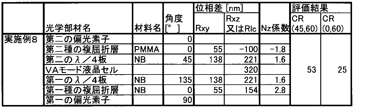


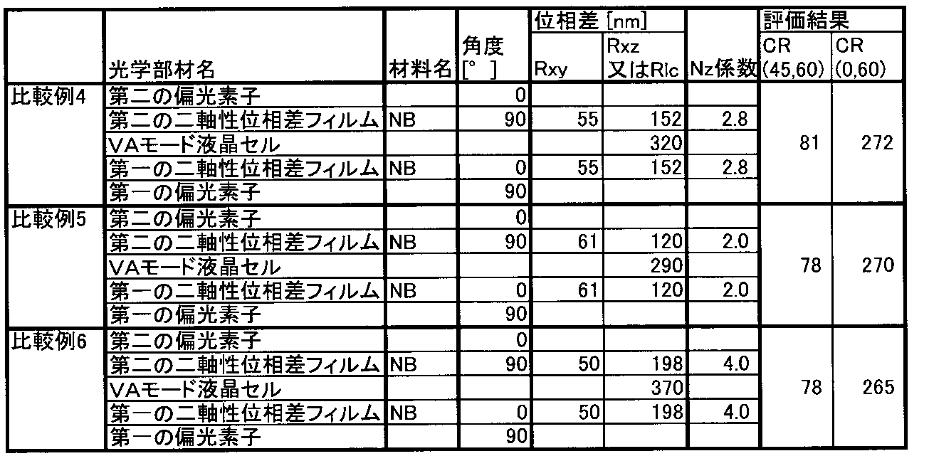
2 複屈折層
11、111、113、115、117 第一の偏光子
12、112、114、116、118 第二の偏光子
31、131、132、133 VAモード液晶セル
101、102、103、104、105、106、107、108 TACフィルム
151 第一種の複屈折層
161 第二種の複屈折層
171、172、173、174、175、176、177 第三種の複屈折層
181、183、185、187、q1 第一のλ/4板
182、184、186、188、q2 第二のλ/4板
191、192 等方性フィルム
201 λ/2板
r1、r4 第一の二軸性位相差フィルム
r2、r2’、r5 第二の二軸性位相差フィルム
r3 第三種の複屈折層
Claims (7)
- 第一の偏光子、第一種の複屈折層、第一のλ/4板、液晶セル、第二のλ/4板、第二種の複屈折層、及び、該第一の偏光子の吸収軸に対して吸収軸が直交する第二の偏光子をこの順に有する液晶表示装置であって、
該第一種の複屈折層は、Nz>0.9を満たし、面内遅相軸が該第一の偏光子の吸収軸に対して直交し、
該第一のλ/4板は、面内遅相軸が該第一の偏光子の吸収軸に対して略45°の角度をなし、
該液晶セルは、液晶セル中の液晶分子を基板面に垂直に配向させることで黒表示を行うものであり、
該第二のλ/4板は、面内遅相軸が該第一のλ/4板の面内遅相軸に対して直交し、
該第二種の複屈折層は、Nz<0.1を満たし、面内遅相軸が該第二の偏光子の吸収軸と平行である
ことを特徴とする液晶表示装置。 - 前記第一種の複屈折層の二軸性パラメータΔNz1を|Nz-1|と定義し、前記第二種の複屈折層の二軸性パラメータΔNz2を|Nz|と定義するとき、|ΔNz1-ΔNz2|≦0.4を満たすことを特徴とする請求項1記載の液晶表示装置。
- 前記第一種の複屈折層の二軸性パラメータΔNz1を|Nz-1|と定義するとき、前記第一種の複屈折層は、2.0≦Nz≦4.0を満たし、かつ、-15+(72-9.6×ΔNz1)≦Rxy≦15+(72-9.6×ΔNz1)を満たすことを特徴とする請求項1又は2記載の液晶表示装置。
- 前記第一種の複屈折層は、2.3≦Nz≦3.3を満たすことを特徴とする請求項3記載の液晶表示装置。
- 前記液晶表示装置は、前記第一のλ/4板と前記液晶セルとの間、及び、前記液晶セルと前記第二のλ/4板との間の少なくとも一方に、Rxy≦10nmかつRxz>0nmを満たす第三種の複屈折層を有することを特徴とする請求項1~4のいずれかに記載の液晶表示装置。
- 前記液晶セルの|Rxz|をRlc、前記第一のλ/4板のNz係数をNzq1、前記第二のλ/4板のNz係数をNzq2と定義するとき、前記第三種の複屈折層は、-50+(Rlc-137.5×(Nzq1+Nzq2-1))≦Rxz≦50+(Rlc-137.5×(Nzq1+Nzq2-1))を満たすことを特徴とする請求項5記載の液晶表示装置。
- 前記第一のλ/4板のNz係数をNzq1、前記第二のλ/4板のNz係数をNzq2と定義するとき、前記第一のλ/4板及び前記第二のλ/4板は、0.8≦Nzq1+Nzq2≦1.2を満たすことを特徴とする請求項1~6のいずれかに記載の液晶表示装置。
Priority Applications (5)
| Application Number | Priority Date | Filing Date | Title |
|---|---|---|---|
| CN2008801254879A CN101925848B (zh) | 2008-04-07 | 2008-11-28 | 液晶显示装置 |
| JP2010507117A JP4538096B2 (ja) | 2008-04-07 | 2008-11-28 | 液晶表示装置 |
| BRPI0822566A BRPI0822566A2 (pt) | 2008-04-07 | 2008-11-28 | dispositivo de vídeo de cristal líquido |
| US12/863,854 US8174650B2 (en) | 2008-04-07 | 2008-11-28 | Liquid crystal display device having first and second birefringent layers and first and second quarter-wave plates |
| EP08873807A EP2259131B1 (en) | 2008-04-07 | 2008-11-28 | Liquid crystal display |
Applications Claiming Priority (2)
| Application Number | Priority Date | Filing Date | Title |
|---|---|---|---|
| JP2008099526 | 2008-04-07 | ||
| JP2008-099526 | 2008-04-07 |
Publications (1)
| Publication Number | Publication Date |
|---|---|
| WO2009125515A1 true WO2009125515A1 (ja) | 2009-10-15 |
Family
ID=41161655
Family Applications (1)
| Application Number | Title | Priority Date | Filing Date |
|---|---|---|---|
| PCT/JP2008/071698 WO2009125515A1 (ja) | 2008-04-07 | 2008-11-28 | 液晶表示装置 |
Country Status (7)
| Country | Link |
|---|---|
| US (1) | US8174650B2 (ja) |
| EP (2) | EP2273290A3 (ja) |
| JP (2) | JP4538096B2 (ja) |
| CN (1) | CN101925848B (ja) |
| BR (1) | BRPI0822566A2 (ja) |
| RU (1) | RU2444034C1 (ja) |
| WO (1) | WO2009125515A1 (ja) |
Cited By (6)
| Publication number | Priority date | Publication date | Assignee | Title |
|---|---|---|---|---|
| JP2012526297A (ja) * | 2009-05-04 | 2012-10-25 | 東友ファインケム株式会社 | 複合構成偏光板セット及びこれを含むブルー相液晶モード液晶表示装置 |
| JP2012526298A (ja) * | 2009-05-04 | 2012-10-25 | 東友ファインケム株式会社 | 複合構成偏光板セット及びこれを含むブルー相液晶モード液晶表示装置 |
| JP2014228567A (ja) * | 2013-05-17 | 2014-12-08 | 富士フイルム株式会社 | 液晶表示装置 |
| US9274376B2 (en) | 2011-03-31 | 2016-03-01 | Sharp Kabushiki Kaisha | Liquid crystal display device |
| JP2016090863A (ja) * | 2014-11-06 | 2016-05-23 | スタンレー電気株式会社 | 液晶表示装置 |
| US9429791B2 (en) | 2012-01-27 | 2016-08-30 | Sharp Kabushiki Kaisha | Liquid crystal display device |
Families Citing this family (20)
| Publication number | Priority date | Publication date | Assignee | Title |
|---|---|---|---|---|
| CN101910922B (zh) * | 2008-01-16 | 2012-05-30 | 夏普株式会社 | 液晶显示装置 |
| RU2445664C1 (ru) * | 2009-01-27 | 2012-03-20 | Шарп Кабусики Кайся | Жидкокристаллическое устройство формирования изображения |
| BR112012001903A2 (pt) | 2009-07-30 | 2016-03-15 | Sharp Kk | dispositivo de exibição de cristal líquido |
| JP5150701B2 (ja) | 2010-10-13 | 2013-02-27 | 富士フイルム株式会社 | 光学フィルム及び液晶表示装置 |
| KR20120070339A (ko) * | 2010-12-21 | 2012-06-29 | 제일모직주식회사 | 액정 디스플레이 및 편광판 제조방법 |
| CN106918860B (zh) * | 2011-12-19 | 2019-05-28 | Lg化学株式会社 | 偏光板 |
| CN103676322B (zh) * | 2012-09-17 | 2016-07-06 | 北京京东方光电科技有限公司 | 一种液晶显示装置及其相位补偿方法 |
| US10295714B2 (en) * | 2014-09-26 | 2019-05-21 | Zeon Corporation | Elongated circularly polarizing plate, elongated broadband lambda/4 plate, organic electroluminescent display device, and liquid crystal display device |
| US10310286B2 (en) * | 2014-09-26 | 2019-06-04 | Zeon Corporation | Circularly polarizing plate, method for producing same, broadband lambda/4 plate, organic electroluminescent display device, and liquid crystal display device |
| CN104216173A (zh) * | 2014-09-30 | 2014-12-17 | 深圳市华星光电技术有限公司 | 液晶显示装置 |
| CN104317106A (zh) * | 2014-11-20 | 2015-01-28 | 京东方科技集团股份有限公司 | 显示基板及其制造方法和显示装置 |
| KR101915923B1 (ko) * | 2015-01-19 | 2018-11-06 | 가부시키가이샤 오루투스 테크놀로지 | 액정 표시 장치 및 헤드업 디스플레이 장치 |
| JP6712157B2 (ja) | 2016-03-25 | 2020-06-17 | 日東電工株式会社 | 光学補償層付偏光板およびそれを用いた有機elパネル |
| JP6712161B2 (ja) * | 2016-03-30 | 2020-06-17 | 日東電工株式会社 | 光学補償層付偏光板およびそれを用いた有機elパネル |
| KR102290943B1 (ko) * | 2016-03-31 | 2021-08-17 | 스미또모 가가꾸 가부시키가이샤 | 편광판의 세트 및 그것을 이용한 ips 모드 액정 표시 장치 |
| CN106094348B (zh) * | 2016-08-19 | 2019-05-03 | 深圳市华星光电技术有限公司 | 液晶面板及具有该液晶面板的液晶显示器 |
| JP2019197181A (ja) * | 2018-05-11 | 2019-11-14 | 住友化学株式会社 | 偏光板および表示装置 |
| CN110908169B (zh) * | 2018-09-14 | 2022-10-04 | 夏普株式会社 | 液晶显示面板 |
| US11169380B2 (en) | 2019-08-15 | 2021-11-09 | Magic Leap, Inc. | Ghost image mitigation in see-through displays with pixel arrays |
| KR20210064475A (ko) * | 2019-11-25 | 2021-06-03 | 삼성디스플레이 주식회사 | 표시 장치 |
Citations (5)
| Publication number | Priority date | Publication date | Assignee | Title |
|---|---|---|---|---|
| JP2002040428A (ja) | 1999-09-28 | 2002-02-06 | Stanley Electric Co Ltd | 液晶表示装置 |
| JP2002055342A (ja) * | 2000-05-31 | 2002-02-20 | Sharp Corp | 液晶表示装置 |
| JP2003186017A (ja) | 2001-10-12 | 2003-07-03 | Fujitsu Display Technologies Corp | 液晶表示装置 |
| JP2003207782A (ja) | 2002-01-11 | 2003-07-25 | Stanley Electric Co Ltd | 垂直配向型液晶表示装置 |
| JP2005326818A (ja) * | 2004-04-16 | 2005-11-24 | Sharp Corp | 円偏光板及び液晶表示装置 |
Family Cites Families (33)
| Publication number | Priority date | Publication date | Assignee | Title |
|---|---|---|---|---|
| GB9322948D0 (en) * | 1993-11-08 | 1994-01-05 | Varintelligent Bvi Ltd | Liquid crystal display |
| US6195140B1 (en) | 1997-07-28 | 2001-02-27 | Sharp Kabushiki Kaisha | Liquid crystal display in which at least one pixel includes both a transmissive region and a reflective region |
| US6330047B1 (en) | 1997-07-28 | 2001-12-11 | Sharp Kabushiki Kaisha | Liquid crystal display device and method for fabricating the same |
| JP3410666B2 (ja) | 1998-07-16 | 2003-05-26 | シャープ株式会社 | 液晶表示装置 |
| JP3410663B2 (ja) | 1998-07-14 | 2003-05-26 | シャープ株式会社 | 液晶表示装置 |
| US6295109B1 (en) | 1997-12-26 | 2001-09-25 | Sharp Kabushiki Kaisha | LCD with plurality of pixels having reflective and transmissive regions |
| US6552767B1 (en) | 1999-02-15 | 2003-04-22 | Citizen Watch Co., Ltd. | Liquid-crystal display |
| JP2003114325A (ja) * | 2001-10-03 | 2003-04-18 | Nitto Denko Corp | 積層1/4波長板、円偏光板及びこれを用いた液晶表示装置、ならびにその製造方法 |
| TW588171B (en) | 2001-10-12 | 2004-05-21 | Fujitsu Display Tech | Liquid crystal display device |
| AU2002366720A1 (en) | 2001-12-12 | 2003-07-09 | Merck Patent Gmbh | Biaxial film |
| JP3873869B2 (ja) | 2002-02-26 | 2007-01-31 | ソニー株式会社 | 液晶表示装置及びその製造方法 |
| JP3788421B2 (ja) | 2002-04-02 | 2006-06-21 | セイコーエプソン株式会社 | 液晶表示装置およびその製造方法ならびに電子機器 |
| TWI226961B (en) * | 2003-01-30 | 2005-01-21 | Chi Mei Optoelectronics Corp | Multi-domain vertical alignment LCD using circular polarized light |
| JP4329983B2 (ja) | 2003-02-05 | 2009-09-09 | 大日本印刷株式会社 | 液晶ディスプレイ |
| JP4449335B2 (ja) * | 2003-05-07 | 2010-04-14 | セイコーエプソン株式会社 | 液晶表示装置および電子機器 |
| TWI305285B (en) * | 2003-05-08 | 2009-01-11 | Au Optronics Corp | Wide view angle liquid crystal display |
| TWI371620B (en) * | 2003-11-21 | 2012-09-01 | Zeon Corp | Liquid crystal display apparatus (1) |
| JP2005173585A (ja) * | 2003-11-21 | 2005-06-30 | Nippon Zeon Co Ltd | 液晶表示装置 |
| TWI268372B (en) * | 2004-03-26 | 2006-12-11 | Nitto Denko Corp | IPS mode liquid crystal display to realize a high contrast ratio over a wide range by laminating a polarizing plate and a retardation film to form an optical film |
| JP4228973B2 (ja) * | 2004-04-08 | 2009-02-25 | セイコーエプソン株式会社 | 液晶表示装置および電子機器 |
| JP2006251050A (ja) * | 2005-03-08 | 2006-09-21 | Toshiba Matsushita Display Technology Co Ltd | 液晶表示素子 |
| KR100762034B1 (ko) * | 2005-05-06 | 2007-09-28 | 비오이 하이디스 테크놀로지 주식회사 | Ocb 모드 액정표시장치 |
| JP2006323069A (ja) | 2005-05-18 | 2006-11-30 | Fujifilm Holdings Corp | 光学補償シート、その製造方法ならびにそれを用いた偏光板及び液晶表示装置 |
| JP2007101874A (ja) * | 2005-10-04 | 2007-04-19 | Toshiba Matsushita Display Technology Co Ltd | 液晶表示素子 |
| WO2007063629A1 (ja) | 2005-12-02 | 2007-06-07 | Sharp Kabushiki Kaisha | 液晶表示装置 |
| JP2007171231A (ja) * | 2005-12-19 | 2007-07-05 | Epson Imaging Devices Corp | 液晶装置及び電子機器 |
| JP4909594B2 (ja) * | 2006-01-17 | 2012-04-04 | 東芝モバイルディスプレイ株式会社 | 液晶表示装置 |
| CN101078839A (zh) * | 2006-05-24 | 2007-11-28 | 日东电工株式会社 | 液晶板和液晶显示装置 |
| TW200821691A (en) * | 2006-07-26 | 2008-05-16 | Toshiba Matsushita Display Tec | Liquid crystal display device |
| JP4692464B2 (ja) | 2006-10-16 | 2011-06-01 | 株式会社デンソー | 車両用交流発電機 |
| CN101568859B (zh) | 2006-11-17 | 2011-04-13 | 新日本石油株式会社 | 椭圆偏振器和使用其的垂直取向型液晶显示装置 |
| JP4878306B2 (ja) * | 2007-02-09 | 2012-02-15 | 株式会社 日立ディスプレイズ | 液晶表示装置 |
| CN101910922B (zh) | 2008-01-16 | 2012-05-30 | 夏普株式会社 | 液晶显示装置 |
-
2008
- 2008-11-28 EP EP10008685A patent/EP2273290A3/en not_active Withdrawn
- 2008-11-28 BR BRPI0822566A patent/BRPI0822566A2/pt not_active IP Right Cessation
- 2008-11-28 JP JP2010507117A patent/JP4538096B2/ja active Active
- 2008-11-28 RU RU2010145180/28A patent/RU2444034C1/ru not_active IP Right Cessation
- 2008-11-28 CN CN2008801254879A patent/CN101925848B/zh active Active
- 2008-11-28 WO PCT/JP2008/071698 patent/WO2009125515A1/ja active Application Filing
- 2008-11-28 US US12/863,854 patent/US8174650B2/en not_active Expired - Fee Related
- 2008-11-28 EP EP08873807A patent/EP2259131B1/en not_active Not-in-force
-
2010
- 2010-05-10 JP JP2010108635A patent/JP5265614B2/ja active Active
Patent Citations (5)
| Publication number | Priority date | Publication date | Assignee | Title |
|---|---|---|---|---|
| JP2002040428A (ja) | 1999-09-28 | 2002-02-06 | Stanley Electric Co Ltd | 液晶表示装置 |
| JP2002055342A (ja) * | 2000-05-31 | 2002-02-20 | Sharp Corp | 液晶表示装置 |
| JP2003186017A (ja) | 2001-10-12 | 2003-07-03 | Fujitsu Display Technologies Corp | 液晶表示装置 |
| JP2003207782A (ja) | 2002-01-11 | 2003-07-25 | Stanley Electric Co Ltd | 垂直配向型液晶表示装置 |
| JP2005326818A (ja) * | 2004-04-16 | 2005-11-24 | Sharp Corp | 円偏光板及び液晶表示装置 |
Non-Patent Citations (2)
| Title |
|---|
| See also references of EP2259131A4 * |
| TAKASAKI HIROSHI: ""Kessyo Kogaku"", 1975, MORIKITA PUBLISHING CO., LTD.,, pages: 146 - 163 |
Cited By (6)
| Publication number | Priority date | Publication date | Assignee | Title |
|---|---|---|---|---|
| JP2012526297A (ja) * | 2009-05-04 | 2012-10-25 | 東友ファインケム株式会社 | 複合構成偏光板セット及びこれを含むブルー相液晶モード液晶表示装置 |
| JP2012526298A (ja) * | 2009-05-04 | 2012-10-25 | 東友ファインケム株式会社 | 複合構成偏光板セット及びこれを含むブルー相液晶モード液晶表示装置 |
| US9274376B2 (en) | 2011-03-31 | 2016-03-01 | Sharp Kabushiki Kaisha | Liquid crystal display device |
| US9429791B2 (en) | 2012-01-27 | 2016-08-30 | Sharp Kabushiki Kaisha | Liquid crystal display device |
| JP2014228567A (ja) * | 2013-05-17 | 2014-12-08 | 富士フイルム株式会社 | 液晶表示装置 |
| JP2016090863A (ja) * | 2014-11-06 | 2016-05-23 | スタンレー電気株式会社 | 液晶表示装置 |
Also Published As
| Publication number | Publication date |
|---|---|
| EP2273290A2 (en) | 2011-01-12 |
| EP2273290A3 (en) | 2011-03-23 |
| JP5265614B2 (ja) | 2013-08-14 |
| CN101925848B (zh) | 2012-11-21 |
| CN101925848A (zh) | 2010-12-22 |
| EP2259131A1 (en) | 2010-12-08 |
| RU2444034C1 (ru) | 2012-02-27 |
| US20100289988A1 (en) | 2010-11-18 |
| BRPI0822566A2 (pt) | 2019-09-24 |
| EP2259131A4 (en) | 2011-03-23 |
| JP2010211230A (ja) | 2010-09-24 |
| US8174650B2 (en) | 2012-05-08 |
| EP2259131B1 (en) | 2012-06-20 |
| JPWO2009125515A1 (ja) | 2011-07-28 |
| JP4538096B2 (ja) | 2010-09-08 |
Similar Documents
| Publication | Publication Date | Title |
|---|---|---|
| JP4538096B2 (ja) | 液晶表示装置 | |
| JP4669909B2 (ja) | 液晶表示装置 | |
| JP4792545B2 (ja) | 液晶表示装置 | |
| JP5000729B2 (ja) | 液晶表示装置の製造方法、及び、液晶表示装置 | |
| JP5330529B2 (ja) | 液晶表示装置 | |
| US8179508B2 (en) | Liquid crystal display device having first and second polarizers and first and second birefringent layers | |
| JP5259824B2 (ja) | 液晶表示装置 | |
| WO2012133137A1 (ja) | 液晶表示装置 | |
| WO2012090769A1 (ja) | 光学素子、及び、液晶表示装置 | |
| US20090002609A1 (en) | Liquid crystal display device | |
| WO2013111867A1 (ja) | 液晶表示装置 | |
| WO2012133155A1 (ja) | 液晶表示装置 | |
| WO2012105428A1 (ja) | 液晶表示装置 | |
| WO2012133140A1 (ja) | 液晶表示装置 | |
| WO2012133141A1 (ja) | 液晶表示装置 |
Legal Events
| Date | Code | Title | Description |
|---|---|---|---|
| WWE | Wipo information: entry into national phase |
Ref document number: 200880125487.9 Country of ref document: CN |
|
| 121 | Ep: the epo has been informed by wipo that ep was designated in this application |
Ref document number: 08873807 Country of ref document: EP Kind code of ref document: A1 |
|
| WWE | Wipo information: entry into national phase |
Ref document number: 2010507117 Country of ref document: JP |
|
| WWE | Wipo information: entry into national phase |
Ref document number: 2285/KOLNP/2010 Country of ref document: IN |
|
| WWE | Wipo information: entry into national phase |
Ref document number: 12863854 Country of ref document: US |
|
| WWE | Wipo information: entry into national phase |
Ref document number: 2008873807 Country of ref document: EP |
|
| NENP | Non-entry into the national phase |
Ref country code: DE |
|
| WWE | Wipo information: entry into national phase |
Ref document number: 2010145180 Country of ref document: RU |
|
| ENP | Entry into the national phase |
Ref document number: PI0822566 Country of ref document: BR Kind code of ref document: A2 Effective date: 20101007 |