WO2009122913A1 - 熱処理装置 - Google Patents
熱処理装置 Download PDFInfo
- Publication number
- WO2009122913A1 WO2009122913A1 PCT/JP2009/055325 JP2009055325W WO2009122913A1 WO 2009122913 A1 WO2009122913 A1 WO 2009122913A1 JP 2009055325 W JP2009055325 W JP 2009055325W WO 2009122913 A1 WO2009122913 A1 WO 2009122913A1
- Authority
- WO
- WIPO (PCT)
- Prior art keywords
- heat treatment
- processing container
- treatment apparatus
- irradiation window
- heating
- Prior art date
- Legal status (The legal status is an assumption and is not a legal conclusion. Google has not performed a legal analysis and makes no representation as to the accuracy of the status listed.)
- Ceased
Links
Images


Classifications
-
- H—ELECTRICITY
- H10—SEMICONDUCTOR DEVICES; ELECTRIC SOLID-STATE DEVICES NOT OTHERWISE PROVIDED FOR
- H10P—GENERIC PROCESSES OR APPARATUS FOR THE MANUFACTURE OR TREATMENT OF DEVICES COVERED BY CLASS H10
- H10P72/00—Handling or holding of wafers, substrates or devices during manufacture or treatment thereof
- H10P72/04—Apparatus for manufacture or treatment
- H10P72/0431—Apparatus for thermal treatment
- H10P72/0436—Apparatus for thermal treatment mainly by radiation
-
- H—ELECTRICITY
- H10—SEMICONDUCTOR DEVICES; ELECTRIC SOLID-STATE DEVICES NOT OTHERWISE PROVIDED FOR
- H10P—GENERIC PROCESSES OR APPARATUS FOR THE MANUFACTURE OR TREATMENT OF DEVICES COVERED BY CLASS H10
- H10P72/00—Handling or holding of wafers, substrates or devices during manufacture or treatment thereof
- H10P72/04—Apparatus for manufacture or treatment
- H10P72/0431—Apparatus for thermal treatment
- H10P72/0434—Apparatus for thermal treatment mainly by convection
Definitions
- the present invention relates to a heat treatment apparatus for performing a predetermined heat treatment such as annealing on an object to be processed such as a semiconductor wafer.
- This annealing process is used to stabilize the characteristics of the thin film formed in the previous process or the surface of the semiconductor wafer doped with impurities.
- an annealing process is performed at a high temperature of about 1000 ° C. in order to modify and stabilize the silicon nitride film. Is called.
- annealing treatment when a silicon oxide film formed on the surface of a semiconductor wafer is modified and stabilized, or a polycrystalline silicon thin film formed on the surface of a glass substrate is melted and solidified to be a single crystal
- an annealing process is known in which heat treatment is performed at a high temperature of about 1000 ° C.
- the semiconductor wafer is introduced into a processing container having a transparent irradiation window, and a heating lamp or a laser element disposed outside the irradiation window is used.
- the generated heat rays are introduced into the processing container through the irradiation window, and the annealing treatment is performed by irradiating and heating the semiconductor wafer with the heat rays.
- a dummy wafer formed so as to have the same form as this semiconductor wafer is installed in parallel with the semiconductor wafer supported as described above in the vertical direction, Heating lamps that can be controlled independently as heating means are arranged on both the upper and lower sides, and while monitoring the temperature of the simulated wafer with a radiation thermometer, the upper and lower heating are performed so that the desired temperature and temperature distribution are obtained.
- An apparatus for controlling the means in exactly the same way is also known (Japanese Patent Laid-Open No. 2006-5177 (Patent Document 3)).
- the temperature control using the pseudo wafer as described above is also called mirroring control.
- a transparent plate-like inexpensive pollution prevention window is provided in parallel inside the irradiation window, and substances generated from a thin film or the like are deposited and deposited on the pollution prevention window, which adheres to the irradiation window itself. It is not allowed to deposit. And this pollution prevention window is exchanged as needed.
- the film thickness near the central part of the semiconductor wafer is reduced and the film thickness near the peripheral part is increased, or vice versa.
- the film thickness in the vicinity increases and the film thickness in the vicinity of the peripheral area decreases, and the in-plane uniformity of the film thickness after the annealing process may decrease.
- a heating lamp for irradiating the semiconductor wafer surface is divided into a plurality of zones, for example, an inner zone and an outer zone, for example, concentrically, and the irradiation amount can be individually controlled for each zone. Has been done.
- the present invention has been made in consideration of such points, and by providing a light shielding part that partially or completely blocks the transmission of heat rays to the film deposition prevention member, fogging occurs in the irradiation window.
- An object of the present invention is to provide a heat treatment apparatus capable of maintaining high in-plane uniformity of the thickness of a thin film after heat treatment while preventing this.
- Another object of the present invention is to provide a film-depositing member locally corresponding to a region where a large amount of the substance released from the object adheres, and the irradiation window is fogged while maintaining high irradiation efficiency.
- An object of the present invention is to provide a heat treatment apparatus capable of suppressing the generation.
- the inventors of the present invention are able to maintain high in-plane uniformity of film thickness by reducing the amount of heat rays irradiated to a region where a thin film formed on a semiconductor wafer is thickened by annealing. By discovering that deposits attached to the irradiation window can be greatly reduced by selectively providing a film deposition prevention member in a region where a large amount of material released from the thin film formed on the wafer adheres.
- the present invention has been achieved.
- the present invention provides a heat treatment apparatus for performing a predetermined heat treatment on an object to be processed, a processing container capable of accommodating the object to be processed and having a ceiling portion, and provided in the processing container.
- a gas supply means that is provided in the processing container and supplies a predetermined gas into the processing container; an exhaust means that is provided in the processing container and exhausts the atmosphere in the processing container; the support means; and the first A heat treatment apparatus comprising a film deposition member provided between the irradiation window and a light shielding portion formed on a part of the heat ray for blocking a part or all of the heat ray.
- the film thickness of the thin film after the heat treatment is prevented while preventing the irradiation window from being fogged. In-plane uniformity can be maintained high.
- the film deposition preventing member includes a quartz glass plate.
- the light shielding portion is formed in a ring shape around the film deposition member.
- the light shielding part is formed in a circular shape at the center of the film deposition preventing member.
- the light-shielding portion is in an opaque glass state.
- a pressure adjusting communication path that communicates with a space defined between the lower surface of the first irradiation window and the upper surface of the film deposition member is formed in the film deposition member.
- the present invention provides a heat treatment apparatus for performing a predetermined heat treatment on an object to be processed, a processing container capable of accommodating the object to be processed and having a ceiling portion, and provided in the processing container.
- a gas supply means that is provided in the processing container and supplies a predetermined gas into the processing container; an exhaust means that is provided in the processing container and exhausts the atmosphere in the processing container; the support means; and the first A heat treatment apparatus comprising: a film deposition member provided between the irradiation window and a size corresponding to a part of the surface of the object to be processed.
- a film deposition preventing member can be locally provided corresponding to a region where a large amount of the released substance adheres, and it is possible to suppress fogging from occurring in the irradiation window while maintaining high irradiation efficiency.
- the film-adhering member is formed in a ring shape having a size corresponding to the peripheral portion of the object to be processed, and the film-adhering member includes quartz glass formed in a ring shape.
- the film deposition preventing member is formed in a circular shape having a size corresponding to the central portion of the object to be processed, and the film deposition preventing member has a disk-shaped quartz glass.
- the quartz glass is made transparent.
- the quartz glass is in an opaque state in order to block part or all of the heat rays.
- the heating means includes a heating lamp.
- the predetermined heat treatment is an annealing treatment for heating a thin film formed on the surface of the object to be processed.
- the present invention provides a heat treatment apparatus for performing a predetermined heat treatment on an object to be processed, a processing container capable of accommodating the object to be processed and having a ceiling part and a bottom part, and provided in the processing container, A supporting means for supporting a body, a simulated object to be processed which is above the object to be processed and is opposed to the object to be processed, and a first part provided on the ceiling portion of the processing container.
- the temperature measuring device includes a radiation thermometer provided to face the upper surface of the simulated workpiece.
- the support means has a rotation mechanism that rotates the object to be processed.
- the dummy workpiece is fixedly provided.
- the distance between the simulated object to be processed and the first heating means is set to be the same as the distance between the object to be processed and the second heating means.
- the temperature control unit controls the first heating unit and the second heating unit to emit the same amount of heat.
- the heating means includes a heating lamp.
- the predetermined heat treatment is an annealing treatment for heating a thin film formed on the surface of the object to be processed.
- the in-plane uniformity of the thickness of the thin film after the heat treatment can be kept high while preventing the irradiation window from being fogged.
- FIG. 1 is a cross-sectional view showing a first embodiment of a heat treatment apparatus according to the present invention.
- 2A and 2B are plan views showing a film deposition preventing member used in the heat treatment apparatus shown in FIG.
- FIGS. 3A and 3B are views showing the relationship between the change in the film thickness formed on the object to be processed and the film deposition preventing member used.
- FIG. 4 is a sectional view showing a second embodiment of the heat treatment apparatus according to the present invention.
- FIG. 5 is an enlarged cross-sectional view showing a main part of a third embodiment of the heat treatment apparatus according to the present invention.
- FIG. 6 is an enlarged cross-sectional view showing a main part of a fourth embodiment of the heat treatment apparatus according to the present invention.
- FIG. 7A and 7B are plan views showing a film deposition preventing member used in the fourth embodiment.
- FIG. 8 is an enlarged cross-sectional view showing a main part of a fifth embodiment of the heat treatment apparatus according to the present invention.
- FIG. 9A and FIG. 9B are plan views showing a film deposition preventing member used in the fifth embodiment.
- FIG. 10 is a sectional view showing a sixth embodiment of the heat treatment apparatus of the present invention.
- FIG. 1 is a cross-sectional view showing a first embodiment of a heat treatment apparatus according to the present invention
- FIG. 2 is a plan view showing a film deposition member used in the heat treatment apparatus shown in FIG. 1
- FIG. 3 is formed on an object to be treated. It is a figure which shows the relationship between the change of a film thickness, and the film
- the heat treatment apparatus 4 has a processing container 6 formed into a cylindrical shape from an aluminum alloy or the like.
- An opening 8 for loading and unloading a semiconductor wafer W as an object to be processed is provided in the side wall of the processing container 6, and a gate valve 10 that can be opened and closed in an airtight manner is provided in the opening 8. .
- gas supply means 12 for supplying a predetermined gas necessary for heat treatment such as annealing, for example, N 2 or O 2, etc., is provided in the side wall of the processing container 6.
- a gas supply nozzle 12A made of, for example, quartz is provided through the side wall of the processing vessel 6, and the gas is supplied while the flow rate is controlled by a flow rate controller such as a mass flow controller (not shown). It can be done.
- a quartz shower head structure or the like may be used.
- an exhaust port 14 is provided at the bottom of the processing container 6.
- the exhaust port 14 is connected to an exhaust means 20 in which a pressure adjusting valve 17 and an exhaust pump 18 such as a vacuum pump are sequentially connected to an exhaust passage 16 to exhaust the atmosphere in the processing vessel 6, for example, It can be evacuated.
- a pressure adjusting valve 17 and an exhaust pump 18 such as a vacuum pump are sequentially connected to an exhaust passage 16 to exhaust the atmosphere in the processing vessel 6, for example, It can be evacuated.
- various pressure control from atmospheric pressure to a high vacuum state is possible for the inside of the processing container 6 according to the processing mode.
- the processing container 6 has a ceiling portion 6A, and a large-diameter opening 22A is formed in the ceiling portion 6A.
- a first irradiation window 26A made of, for example, a transparent quartz plate is airtightly attached and fixed to the opening 22A through a seal member 24A such as an O-ring.
- a first heating means 28A is provided outside the first irradiation window 26A.
- the first heating means 28A has a lamp house 30A whose inner surface is a reflective surface.
- a plurality of heating lamps 32A made of, for example, halogen lamps arranged in a straight tube are arranged in parallel, and the semiconductor wafer W is heated by radiation (heat rays) from these heating lamps 32A. To get.
- a spherical lamp may be used as the halogen lamp.
- a temperature measuring device 34 made of, for example, a pyro sensor (radiation thermometer) is provided at the bottom 6B of the processing container 6.
- the measured value of the temperature measuring device 34 is input to a temperature control unit 36 made of, for example, a microcomputer, and the power supplied to the first heating means 28A is controlled based on the measured value to bring the semiconductor wafer to a predetermined temperature. It can be controlled.
- the first heating means 28A may be concentrically divided into, for example, an inner circumferential zone and an outer circumferential zone so that the temperature can be individually controlled for each zone.
- support means 38 for supporting the semiconductor wafer W is provided.
- the support means 38 also serves as a part of a lifting mechanism 40 that lifts and lowers the semiconductor wafer W when the semiconductor wafer W is loaded and unloaded.
- the support means 38 includes a large-diameter circular ring-shaped lifting plate 42 made of, for example, quartz (quartz).
- the elevating plate 42 is mounted on a large-diameter circular ring-shaped mounting plate 44 which is also made of quartz.
- the ring-shaped mounting plate 44 that supports the elevating plate 42 is not fixed to the side wall of the processing container 6 but is rotatable by a rotating mechanism 46 here.
- the rotating mechanism 46 includes a plurality of rotating rollers 50 that are rotatably supported on the side wall of the processing container 6 via bearings 48. At least three rotating rollers 50 (two in the illustrated example) are provided at equal intervals along the circumferential direction of the processing container 6.
- the bearing 48 is sealed with, for example, a magnetic fluid in order to allow the rotation of the rotating roller 50 while maintaining airtightness in the processing container 6.
- Each of the rotating rollers 50 is made of, for example, quartz, and is formed in a truncated cone shape, for example.
- the above-mentioned mounting plate 44 is placed and supported on the upper surface side of each rotating roller 50. By rotating this rotating roller 50, the above-described mounting plate 44 can be rotated in the circumferential direction. It has become.
- a drive motor 52 is connected to one of the three rotary rollers 50.
- a hard receiving member 54 made of, for example, SiC is provided along the circumferential direction of the outer corner of the mounting plate 44, and the rotating roller 50 is brought into direct contact with the receiving member 54. .
- the receiving member 54 By providing the receiving member 54, the generation of particles is prevented here.
- a positioning hole 56 is formed in a part of the mounting plate 44, and a light emitter 58 that emits laser light and a light receiver 60 that receives the laser light are provided above and below the positioning hole 56, for example. Yes.
- the home position of the mounting plate 44 can be detected and the position in the rotation direction can be recognized.
- the mounting plate 44 may be fixed to the side wall side of the processing container 6 so as not to rotate.
- a plurality of, for example, three (only two in the illustrated example) support arms 62 made of quartz extend from the ring-shaped lifting plate 42 toward the center thereof.
- the support arms 62 are arranged at equal intervals along the circumferential direction of the elevating plate 42.
- the tip of each support arm 62 is provided with a support pin 64 made of, for example, quartz, and the upper end of each support pin 64 is brought into contact with the peripheral portion on the back surface of the semiconductor wafer W, thereby the semiconductor wafer. Supports W.
- a lifting actuator 66 is provided on the bottom 6B of the processing vessel 6 as a part of the lifting mechanism 40.
- three lift actuators 66 are provided along the circumferential direction of the bottom 6B.
- Each lifting / lowering actuator 66 is provided with a lifting / lowering rod 70 inserted through the through hole 68 of the container bottom 6B in a loosely fitted state.
- an insertion hole 72 for passing the lifting rod 70 is also formed in the mounting plate 44 described above.
- the elevating plate 42 can be pushed upward by inserting the upper end of the elevating rod 70 into the insertion hole 72.
- the lift mechanism 66 is formed by the lift actuator 66 and the support means 38.
- a metal bellows 74 that can be extended and contracted is interposed in the bottom through portion of the lifting rod 70, and the lifting rod 70 can be allowed to move up and down while maintaining airtightness in the processing container 6. It is like that.
- the film deposition preventing member 80 is entirely made of, for example, a circular quartz glass plate 82 having a large heat resistance and corrosion resistance, and is set to a size that covers the entire surface of the first irradiation window 26A. ing. In other words, the film deposition preventing member 80 is set to have a diameter equal to or larger than that of the semiconductor wafer W so as to cover the entire surface of the semiconductor wafer W.
- membrane prevention member 80 is detachably attached and fixed to the said ceiling part 6A with the volt
- the quartz glass plate 82 can be replaced when a certain amount of deposits are deposited on the quartz glass plate 82.
- the bolt 84 is made of a material that does not cause metal contamination, such as an aluminum alloy or a ceramic material.
- the quartz glass plate 82 is formed with a light shielding portion 86 for blocking part or all of the irradiation light (heat rays) from the first heating means 28A.
- the light shielding portion 86 is formed in a ring shape on the peripheral portion of the quartz glass plate 82. (Region shown by hatching in FIG. 2). Then, the region other than the light shielding portion 86, that is, the transmission region 88 on the center side here is in a state transparent to the heat rays, and the heat rays passing therethrough are transmitted without being lost, and the semiconductor wafer W is transmitted. It can be heated.
- the light shielding portion 86 is in an opaque glass state in order to suppress the heat dose passing therethrough.
- the opaque glass state includes a semi-transparent state in which a part of the irradiation light can be passed from a state where the irradiation light is completely blocked, and the transmissivity thereof is on the semiconductor wafer W.
- the thickness is determined based on the film thickness characteristics of the thin film to be annealed formed by annealing.
- the light shielding portion 86 is in a frosted glass state, a frosted glass state, a frosted glass state, a foamed glass state in which bubbles are included, or a milky white turbid glass state. It is preferable to set a state in which the irradiation light is diffusely reflected.
- the light shielding part 86 may be configured to coat, for example, magnesium oxide as a light shielding material on transparent glass.
- the quartz glass plate 82 is provided with a pressure adjustment series for adjusting the pressure in the space 90 defined between the lower surface of the first irradiation window 26A and the upper surface of the quartz glass plate 82 (pressure release).
- a passage 92 is formed (see FIG. 1).
- the pressure adjusting communication path 92 is formed by a minute through hole 92A.
- a minute communication groove or the like extending in the radial direction may be formed in the periphery of the upper surface of the quartz glass plate 82.
- the quartz glass plate 82 is attached to the ceiling 6 ⁇ / b> A, it may be supported from the side wall of the processing vessel 6.
- the central part of the quartz glass plate 82 is the transmission region 88 and the peripheral part is the light shielding part 86.
- the peripheral part is the light shielding part 86.
- a central portion of the plate 82 serves as a light shielding portion 86 and a peripheral portion serves as a transmission region 88. Accordingly, the different types of film deposition-preventing members 80 shown in FIGS. 2A and 2B can be exchanged and used in accordance with the characteristics of the thin film to be annealed.
- the operation of the entire apparatus for example, control of the semiconductor wafer temperature, the pressure in the container, the supply amount of each gas, and the like is performed by an apparatus control unit 96 formed of a computer.
- a computer-readable program necessary for this control is stored in advance in the storage medium 98.
- the storage medium 98 is composed of, for example, a flexible disk, a CD (Compact Disc), a CD-ROM, a hard disk, a flash memory, or a DVD.
- the semiconductor wafer W is carried into the processing container 6, the semiconductor wafer W is carried into the processing container 6 from the opened gate valve 10 through the opening 8 by a transfer arm (not shown).
- the elevating actuator 66 of the elevating mechanism 40 is driven to extend the elevating rod 70 upward, thereby pushing up the elevating plate 42 of the support means 38 and raising the support pin 64.
- the semiconductor wafer W carried into the processing chamber 6 by the transfer arm (not shown) is pushed up by the support pins 64 rising from below, whereby the semiconductor wafer W is transferred from the transfer arm to the support pins 64. Passed and held.
- the transfer arm is extracted from the processing container 6, and the lifting rod 70 is lowered while the semiconductor wafer W is held by the support pins 64 as described above.
- the lifting plate 42 is placed on the placement plate 44 as shown in FIG.
- the gate valve 10 is closed to seal the inside of the processing container 6, and necessary gases such as N 2 and O 2 are supplied from the gas supply means 12 into the processing container 6 while controlling the flow rate.
- the exhaust unit 20 is driven to maintain the inside of the processing container 6 in a predetermined pressure atmosphere.
- the rotation roller 50 is rotated, thereby rotating the mounting plate 44 and the elevating plate 42 in the circumferential direction, thereby rotating the semiconductor wafer W in the same plane.
- the respective heating lamps 32A of the first heating means 28A are turned on to perform heat treatment, for example, annealing while maintaining the temperature of the semiconductor wafer W at a predetermined temperature, for example, about 1050 ° C.
- the temperature of the semiconductor wafer W is measured by a temperature measuring device 34 including, for example, a radiation thermometer provided on the container bottom 6B. Based on the value measured by the temperature measuring device 34, the temperature control unit 36 feedback-controls the irradiation light from the first heating means 28A. As a result, the semiconductor wafer W is maintained at a predetermined temperature set in advance.
- a thin film to be annealed in the previous process is formed in advance, and the thin film is heated by the annealing process, and the film quality is modified by the annealing process. Become.
- the thin film is, for example, a silicon oxide film (SiO 2 ) or a silicon nitride film (SiN), and various thin films are subjected to annealing treatment.
- the annealing process conditions depend on the type of thin film to be annealed, but the semiconductor wafer temperature is in the range of about 700 to 1050 ° C., and the pressure is 0.1 Torr (13.3 Pa) to 760 Torr (1018 Pa).
- N 2 gas is in the range of 500 to 10,000 sccm
- O 2 gas is in the range of 0 to 100 sccm.
- the semiconductor wafer W on which the thin film is formed is heated to, for example, about 1050 ° C. during the annealing process, for example, a substance in which the thin film is decomposed is generated from the thin film, or any substance is generated from each member in the processing container 6 May occur.
- the generated substance rises as shown by an arrow 99 and deposits and accumulates on the irradiation window to cause fogging. Costs were also rising.
- a quartz glass plate 82 that can be easily replaced is formed above the semiconductor wafer W, that is, below the first irradiation window 26A provided on the ceiling 6A.
- a film deposition preventing member 80 is provided. As a result, substances generated from the thin film and the like are deposited on the lower surface of the quartz glass plate 82, and can be prevented from being deposited on the first irradiation window 26A.
- the quartz glass plate 82 is replaced with a new one.
- the maintenance work in this case can be performed very quickly and easily because the quartz glass plate 82 is simply replaced. Therefore, it is possible to prevent the operating rate of the apparatus from decreasing.
- the peripheral portion of the thin film on the surface of the semiconductor wafer W becomes thicker than the central portion after the above-described annealing treatment (after heat treatment). Or, conversely, the peripheral part may be thinner than the central part, and the in-plane uniformity of the film thickness may be significantly reduced.
- a part of the quartz glass plate 82 which is the film adhesion preventing member 80 is shielded from a part or all of the heat rays (irradiation light) from the first heating means 28A. Since the portion 86 is provided to reduce the transmittance and the radiation rate of the portion to suppress the amount of heat entering the corresponding portion of the surface of the semiconductor wafer W, an increase in the thickness of the portion can be reduced. As a result, the in-plane uniformity of the film thickness can be kept high.
- the thin film 110 formed on the semiconductor wafer W has a characteristic that the central portion is thin and the peripheral portion is thick after annealing.
- annealing is performed using a film deposition member 80 having a transmission region 88 at the center and a ring-shaped light shielding portion 86 at the periphery. I do.
- the amount of heat (irradiation amount) incident on the peripheral portion of the thin film 110 is reduced and an increase in the thickness of the peripheral portion is suppressed, and the in-plane uniformity of the film thickness after the annealing treatment can be improved.
- the thin film 110 formed on the semiconductor wafer W has a characteristic that the central portion is thick and the peripheral portion is thin after annealing.
- the annealing is performed using the film deposition member 80 having the transmission region 88 in the peripheral portion and the ring-shaped light shielding portion 86 in the central portion. Do.
- the amount of heat (irradiation amount) incident on the central portion of the thin film 110 is reduced, the increase in the thickness of the central portion is suppressed, and the in-plane uniformity of the thickness after the annealing treatment can be improved.
- the pressure in the processing container 6 may be greatly changed.
- a partition is formed between the first irradiation window 26A and the film deposition preventing member 80.
- the pressure in the space 90 is the same as the pressure in the processing container 6 on the side where the semiconductor wafer W is placed by passing the gas through the pressure adjusting communication path 92 formed in the film deposition preventing member 80. Become.
- the force due to the pressure difference does not act on the film deposition preventing member 80, and damage to the film deposition preventing member 80 can be prevented.
- the irradiation window (first In-plane uniformity of the thickness of the thin film after the heat treatment can be kept high while preventing the irradiation window 26A) from being fogged.
- FIG. 4 is a sectional view showing a second embodiment of the heat treatment apparatus according to the present invention.
- the same referential mark is attached
- the dummy wafer 102 as a dummy object to be processed is supported below the semiconductor wafer W so as to face the semiconductor wafer W. Furthermore, a second heating means 28B for heating the simulated wafer 102 is provided below this, that is, at the bottom 6B of the processing container 6. Specifically, a large-diameter opening 22B is formed in the bottom 6B of the processing container 6, and the opening 22B is made of, for example, a transparent quartz plate via a seal member 24B such as an O-ring. The second irradiation window 26B is attached and fixed in an airtight manner.
- the second heating means 28B is provided outside the second irradiation window 26B.
- the second heating means 28B has a lamp house 30B whose inner surface is a reflecting surface.
- a plurality of heating lamps 32B made of, for example, a halogen lamp made of a straight tube are flattened.
- the dummy wafers 102 are arranged in a row so that the dummy wafer 102 can be heated by the radiated light (heat rays) from these heating lamps 32B.
- a spherical lamp may be used as the halogen lamp.
- the lamp house 30B of the second heating means 28B is provided with a temperature measuring device 34 made of, for example, a pyrosensor (radiation thermometer).
- a temperature control unit 36 made of, for example, a microcomputer is connected to the temperature measuring device 34. The measured value of the temperature measuring device 34 is input to the temperature control unit 36, and the semiconductor wafer can be controlled to a predetermined temperature by controlling the input power to the second heating means 28B based on the measured value.
- the second heating unit 28B may be concentrically divided into, for example, an inner circumferential zone and an outer circumferential zone so that the temperature can be individually controlled for each zone.
- the temperature measuring device 34 measures the temperature of the back surface of the simulated wafer 102, and the temperature control unit 36 controls both the first and second heating means 28A and 28B based on the measured value. I am doing so.
- the first and second heating means 28A, 28B are controlled so as to emit irradiation light having the same heat amount, that is, mirroring control is performed.
- the wattage of the heating lamps 32A and 32B of the first and second heating means 28A and 28B is set to be the same, and the distance L2 between the semiconductor wafer W and the second irradiation window 26B is The distance L1 between the pseudo wafer 102 and the first irradiation window 26A is set to the same value, and the thermal conditions are set to be the same.
- the mounting plate 44 is provided with a plurality of support rods 104 made of, for example, quartz extending horizontally in the center direction.
- support rods 104 made of, for example, quartz extending horizontally in the center direction.
- three support rods 104 are provided at equal intervals along the circumferential direction of the mounting plate 44, and the tip portions thereof are bent upward in an L shape.
- the disk-shaped dummy wafer 102 is horizontally supported at the tip of each support rod 104.
- the dummy wafer 102 is formed to have the same form as the semiconductor wafer W.
- a silicon wafer having the same diameter and thickness as the semiconductor wafer W can be used as the pseudo wafer 102.
- a silicon wafer (bare wafer) having nothing formed on the surface is transparent to wavelengths in the infrared region, so that it absorbs the wavelengths in this region and is heated in the same manner as the semiconductor wafer W.
- a coating film made of SiN, SiO 2 or the like is formed on the surface of the pseudo wafer 102.
- each support pin member 106 is attached on the pseudo wafer 102 by welding or the like at equal intervals along the circumferential direction.
- the semiconductor wafer W is supported by the upper end portion of each support pin member 106.
- the dummy wafer 102 is arranged in parallel to the semiconductor wafer W.
- a lift pin 108 that is erected upward is attached to the tip of each support arm 62 that extends from the lifting plate 42.
- the lift pins 108 are provided so as to penetrate upward through the pin holes 110 formed in the dummy wafer 102.
- the semiconductor wafer W is pushed upward to deliver the semiconductor wafer W. Can be done.
- the lift pins 108 are configured as a part of the lifting mechanism 40 that lifts the semiconductor wafer.
- the above-mentioned film deposition preventing member 80 which is a feature of the present invention, is provided below the first irradiation window 26A.
- the configuration and deformation mode of the film deposition preventing member 80 are as described above with reference to FIGS.
- so-called mirroring control is performed as temperature control during annealing of the semiconductor wafer W.
- the temperature of the simulated wafer 102 is monitored by the temperature measuring device 34 so that the simulated wafer 102 has a desired temperature by the second heating unit 28B, and the temperature is controlled by feedback.
- so-called mirroring control is performed so that the electric power supplied to the first heating means 28A at the ceiling and the second heating means 28B at the bottom are exactly the same.
- the temperature of the semiconductor wafer W can be controlled to be the same as the temperature of the dummy wafer 102, and as a result, the temperature of the semiconductor wafer W can be maintained at a desired temperature.
- the power supplied to the upper and lower first and second heating means 28A, 28B is not exactly the same. There is a deviation of the offset value.
- the reason for performing the mirroring control in this way is that the back surface of the dummy wafer 102 is optically stable, whereas the semiconductor wafer W is loaded with various processes performed in the previous process. Therefore, optically constant things are not always carried in, and it is difficult to accurately detect the temperature of such a semiconductor wafer W with the temperature measuring device 34 including a radiation thermometer.
- membrane prevention member 80 since the film
- FIG. 5 is an enlarged cross-sectional view showing the main part of the third embodiment of the heat treatment apparatus according to the present invention, and the other parts are configured as shown in FIGS.
- the same components as those shown in FIGS. 1 to 4 are denoted by the same reference numerals.
- the film deposition member 80 is attached in close contact with the lower surface of the first irradiation window 26 ⁇ / b> A, and this film deposition member 80 is tightened with a bolt 84.
- the holding plate 114 is detachably fixed. In this case, since the space 90 is not formed, it is not necessary to provide the pressure adjusting communication path 92 (see FIG. 1) for preventing the film deposition preventing member 80 from being damaged by the pressure difference.
- the film deposition preventing member 80 is formed in a disk shape having a size so as to cover the entire lower surface of the first irradiation window 26A.
- the size is set to correspond to a part of the surface of the semiconductor wafer W.
- the film deposition preventing member 80 has a diameter substantially equal to that of the semiconductor wafer W, but is formed in a circular ring shape, and in the fifth embodiment, the diameter is considerably smaller than that of the semiconductor wafer W. It has a disc shape.
- FIG. 6 is an enlarged sectional view showing the main part of the fourth embodiment of the heat treatment apparatus according to the present invention
- FIG. 7 is a plan view showing the film deposition member used in the fourth embodiment
- FIG. 8 is as described above.
- FIG. 9 is an enlarged cross-sectional view showing a main part of a fifth embodiment of the heat treatment apparatus according to the present invention.
- the first irradiation window 26A is provided so as to cover a part thereof. The reason is that, according to the experiment, depending on the type of film to be annealed and annealing conditions, an unnecessary thin film is not deposited on the entire surface in a state where the film thickness is uniform on the lower surface of the first irradiation window 26A. This is because there is a case where it adheres and accumulates.
- the film deposition preventing member 80 is made to be the first. This is because it is not necessary to provide the entire surface of the irradiation window 26A.
- a circular ring-shaped quartz glass plate 120 whose outer diameter is substantially the same as that of the first irradiation window 26 ⁇ / b> A. Used.
- the width W1 of the quartz glass plate 120 is determined by the film thickness distribution of an unnecessary adhesion film deposited on the first irradiation window 26A.
- the fourth embodiment is used when an annealing process is performed in which an unnecessary thin film is deposited particularly thickly on the periphery of the lower surface of the first irradiation window 26A.
- the entire circular ring-shaped quartz glass plate 120 may be used as the light shielding portion 86, and conversely, as shown in FIG. 7B, the entire circular ring-shaped quartz glass plate 120. May be used as the transmission region 88.
- the size corresponding to a part of the surface of the object to be processed is provided between the support means 38 for supporting the semiconductor wafer W as the object to be processed and the irradiation window (first irradiation window 26A).
- the film-adhering member 80 made of the quartz glass plate 120 set to, for example the film-adhering member can be locally provided corresponding to the region where a large amount of the substance released from the object to be treated adheres, It is possible to suppress fogging of the irradiation window while maintaining high irradiation efficiency.
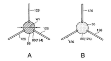
- the outer diameter of the film deposition preventing member 80 is considerably smaller than that of the first irradiation window 26A.
- a circular quartz glass plate 124 is used.
- the small circular quartz glass plate 124 corresponds to the center of the first irradiation window 26A by a plurality of, for example, three support arms 126 extending from the ceiling 6A toward the center of the opening 22A. Supported in position.
- the diameter W2 of the quartz glass plate 124 is determined by the film thickness distribution of unnecessary films deposited on the first irradiation window 26A.
- This fifth embodiment is used when performing an annealing process in which an unnecessary thin film is deposited particularly thickly at the center of the lower surface of the first irradiation window 26A.
- the entire circular quartz glass plate 124 may be used as the light shielding portion 86.
- the entire circular ring-shaped quartz glass plate 124 may be used.
- the transmission region 88 may be used.
- a size corresponding to a part of the surface of the object to be processed is provided between the support means 38 for supporting the semiconductor wafer W as the object to be processed and the irradiation window (first irradiation window 26A).
- the film-adhering member 80 made of the quartz glass plate 124 set in (1) for example, the film-adhering member can be provided locally corresponding to a region where a large amount of the substance released from the object is adhered, It is possible to suppress fogging of the irradiation window while maintaining high irradiation efficiency.
- the film deposition preventing member 80 is provided in order to prevent unnecessary films from adhering to the surface of the first irradiation window 26A.
- the above-described film deposition member 80 is provided. Without using the film adhesion preventing member 80, the installation position of the semiconductor wafer and the dummy wafer is changed up and down, thereby making the dummy wafer also function as the film adhesion preventing member.
- the sixth embodiment is a modified embodiment of the second embodiment shown in FIG. 4 that performs mirroring control.
- FIG. 10 is a sectional view showing a sixth embodiment of the heat treatment apparatus of the present invention.
- the same components as those shown in FIGS. 1 to 4 are denoted by the same reference numerals, and the description thereof is omitted.
- the film adhesion preventing member 80 as described above is not provided, and the installation positions of the semiconductor wafer W and the dummy wafer 102 are switched upside down, Therefore, the dummy wafer 102 is installed immediately above the semiconductor wafer W.
- the semiconductor wafer W is supported by the support pins 64 provided at the tips of the support arms 62 extending from the lifting plate 42 as in the first embodiment shown in FIG.
- the length of the support pin 64 is set slightly shorter than that in the case of FIG.
- the dummy wafer 102 positioned above the semiconductor wafer W is supported by a plurality of support arms 128 extending from the side wall of the processing container 6. Therefore, the dummy wafer 102 is heated by the first heating means 28A located above, and the semiconductor wafer W is heated by the second heating means 28B installed below.
- the temperature measuring device 34 is provided on the first heating means 28A side and measures the temperature on the upper surface side of the simulated wafer 102.
- the temperature control unit 36 performs mirroring control. Become.
- the distance L3 between the simulated wafer 102 and the upper first irradiation window 26A, and the distance L4 between the semiconductor wafer W and the lower second irradiation window 26B. are set to be the same.
- the temperature measuring device 34 measures the temperature of the upper surface of the dummy wafer 102, and the mirroring control as described in the second embodiment shown in FIG. Is called.
- the substance generated from the thin film of the semiconductor wafer W during the annealing process rises as indicated by an arrow 130 and adheres to the lower surface (back surface) of the dummy wafer 102. Therefore, an unnecessary film does not adhere to the surface (upper surface) of the first irradiation window 26A, and fogging can be prevented from occurring.
- the surface state of the upper surface of the dummy wafer 102 is as follows. It is always kept stable, and the accuracy of this temperature measurement can be kept high.
- the dummy wafer 102 as the dummy object to be processed is disposed above the semiconductor wafer W as the object to be processed, and the temperature on the upper surface side of the dummy wafer 102 is set. Since the so-called mirroring control is performed while measuring, the substance generated from the thin film of the semiconductor wafer can be deposited on the lower surface (back surface) of the simulated wafer, and thus the above-mentioned film deposition preventing member 80 is used. Therefore, it is possible to prevent the first irradiation window 26A from being fogged due to an unnecessary attached film.
- the heating lamps 32A and 32B are used as the heating means 28A and 28B.
- scanning may be performed using laser light.
- the thin film to be annealed is any film type that causes unnecessary film adhesion due to heating, and the present invention can be applied to a heat treatment apparatus in which such a film type is formed. it can.
- the semiconductor wafer is described as an example of the object to be processed here, the present invention is not limited thereto, and the present invention can be applied to a glass substrate, an LCD substrate, a ceramic substrate, and the like.
Priority Applications (1)
| Application Number | Priority Date | Filing Date | Title |
|---|---|---|---|
| CN200980100966XA CN101855708B (zh) | 2008-03-31 | 2009-03-18 | 热处理装置 |
Applications Claiming Priority (2)
| Application Number | Priority Date | Filing Date | Title |
|---|---|---|---|
| JP2008089069A JP5077018B2 (ja) | 2008-03-31 | 2008-03-31 | 熱処理装置 |
| JP2008-089069 | 2008-03-31 |
Publications (1)
| Publication Number | Publication Date |
|---|---|
| WO2009122913A1 true WO2009122913A1 (ja) | 2009-10-08 |
Family
ID=41135299
Family Applications (1)
| Application Number | Title | Priority Date | Filing Date |
|---|---|---|---|
| PCT/JP2009/055325 Ceased WO2009122913A1 (ja) | 2008-03-31 | 2009-03-18 | 熱処理装置 |
Country Status (5)
| Country | Link |
|---|---|
| JP (1) | JP5077018B2 (https=) |
| KR (1) | KR20100138984A (https=) |
| CN (1) | CN101855708B (https=) |
| TW (1) | TW200949950A (https=) |
| WO (1) | WO2009122913A1 (https=) |
Cited By (3)
| Publication number | Priority date | Publication date | Assignee | Title |
|---|---|---|---|---|
| JP2012109527A (ja) * | 2010-10-28 | 2012-06-07 | Hitachi Kokusai Electric Inc | 基板処理装置および半導体装置の製造方法 |
| CN105261576A (zh) * | 2014-07-15 | 2016-01-20 | 北京北方微电子基地设备工艺研究中心有限责任公司 | 一种加热腔室及半导体加工设备 |
| FR3142757A1 (fr) * | 2022-12-05 | 2024-06-07 | Annealsys | Four de recuit thermique rapide à uniformité de chauffage améliorée |
Families Citing this family (15)
| Publication number | Priority date | Publication date | Assignee | Title |
|---|---|---|---|---|
| JP5640890B2 (ja) * | 2011-05-23 | 2014-12-17 | ウシオ電機株式会社 | 光照射装置および光照射方法 |
| JP6038503B2 (ja) * | 2011-07-01 | 2016-12-07 | 株式会社日立国際電気 | 基板処理装置及び半導体装置の製造方法 |
| KR101297981B1 (ko) * | 2011-10-07 | 2013-08-23 | (주) 예스티 | 기판의 열처리 장치 |
| JP5964630B2 (ja) * | 2012-03-27 | 2016-08-03 | 株式会社Screenホールディングス | 熱処理装置 |
| US8785815B2 (en) * | 2012-06-22 | 2014-07-22 | Applied Materials, Inc. | Aperture control of thermal processing radiation |
| US11089657B2 (en) * | 2015-03-06 | 2021-08-10 | SCREEN Holdings Co., Ltd. | Light-irradiation heat treatment apparatus |
| JP6518548B2 (ja) * | 2015-08-10 | 2019-05-22 | 東京応化工業株式会社 | 紫外線照射装置、レジストパターン形成装置、紫外線照射方法及びレジストパターン形成方法 |
| JP6546512B2 (ja) * | 2015-11-04 | 2019-07-17 | 株式会社Screenホールディングス | 熱処理装置 |
| CN107706139A (zh) * | 2017-11-13 | 2018-02-16 | 上海华力微电子有限公司 | 一种半导体加工机台的温度控制装置 |
| JP7048372B2 (ja) * | 2018-03-20 | 2022-04-05 | 株式会社Screenホールディングス | 熱処理装置および熱処理方法 |
| KR102737498B1 (ko) | 2019-12-13 | 2024-12-04 | 삼성전자주식회사 | 비-접촉식 온도 센서를 가진 공정 설비 |
| JP7546417B2 (ja) * | 2020-09-09 | 2024-09-06 | 株式会社Screenホールディングス | 熱処理装置 |
| CN115064471B (zh) * | 2022-08-01 | 2023-11-28 | 北京屹唐半导体科技股份有限公司 | 晶圆的热处理装置 |
| CN115411174A (zh) * | 2022-08-30 | 2022-11-29 | 三三智能科技(日照)有限公司 | 一种用于压电薄膜稳定连续退火装置 |
| CN118712105B (zh) * | 2024-08-29 | 2025-02-14 | 一塔半导体(安徽)有限公司 | 一种快速热退火装置 |
Citations (3)
| Publication number | Priority date | Publication date | Assignee | Title |
|---|---|---|---|---|
| JPH09270390A (ja) * | 1996-03-29 | 1997-10-14 | Dainippon Screen Mfg Co Ltd | 基板の光照射式熱処理装置 |
| JPH10321547A (ja) * | 1997-05-22 | 1998-12-04 | Kokusai Electric Co Ltd | 熱処理装置 |
| JP2006005177A (ja) * | 2004-06-17 | 2006-01-05 | Tokyo Electron Ltd | 熱処理装置 |
Family Cites Families (1)
| Publication number | Priority date | Publication date | Assignee | Title |
|---|---|---|---|---|
| JP4200844B2 (ja) * | 2003-08-11 | 2008-12-24 | 東京エレクトロン株式会社 | 熱処理装置 |
-
2008
- 2008-03-31 JP JP2008089069A patent/JP5077018B2/ja not_active Expired - Fee Related
-
2009
- 2009-03-18 CN CN200980100966XA patent/CN101855708B/zh not_active Expired - Fee Related
- 2009-03-18 KR KR1020107021779A patent/KR20100138984A/ko not_active Ceased
- 2009-03-18 WO PCT/JP2009/055325 patent/WO2009122913A1/ja not_active Ceased
- 2009-03-30 TW TW098110446A patent/TW200949950A/zh unknown
Patent Citations (3)
| Publication number | Priority date | Publication date | Assignee | Title |
|---|---|---|---|---|
| JPH09270390A (ja) * | 1996-03-29 | 1997-10-14 | Dainippon Screen Mfg Co Ltd | 基板の光照射式熱処理装置 |
| JPH10321547A (ja) * | 1997-05-22 | 1998-12-04 | Kokusai Electric Co Ltd | 熱処理装置 |
| JP2006005177A (ja) * | 2004-06-17 | 2006-01-05 | Tokyo Electron Ltd | 熱処理装置 |
Cited By (4)
| Publication number | Priority date | Publication date | Assignee | Title |
|---|---|---|---|---|
| JP2012109527A (ja) * | 2010-10-28 | 2012-06-07 | Hitachi Kokusai Electric Inc | 基板処理装置および半導体装置の製造方法 |
| CN105261576A (zh) * | 2014-07-15 | 2016-01-20 | 北京北方微电子基地设备工艺研究中心有限责任公司 | 一种加热腔室及半导体加工设备 |
| FR3142757A1 (fr) * | 2022-12-05 | 2024-06-07 | Annealsys | Four de recuit thermique rapide à uniformité de chauffage améliorée |
| EP4382840A1 (fr) * | 2022-12-05 | 2024-06-12 | Annealsys | Four de recuit thermique rapide a uniformite de chauffage amelioree |
Also Published As
| Publication number | Publication date |
|---|---|
| TW200949950A (en) | 2009-12-01 |
| JP5077018B2 (ja) | 2012-11-21 |
| KR20100138984A (ko) | 2010-12-31 |
| CN101855708A (zh) | 2010-10-06 |
| CN101855708B (zh) | 2012-10-10 |
| JP2009246061A (ja) | 2009-10-22 |
Similar Documents
| Publication | Publication Date | Title |
|---|---|---|
| JP5077018B2 (ja) | 熱処理装置 | |
| TWI649821B (zh) | 在晶圓處理系統內進行低溫測量的設備與方法 | |
| JP6286463B2 (ja) | 高温測定のための加熱源反射フィルタを含む装置 | |
| JP5982758B2 (ja) | マイクロ波照射装置 | |
| JP4540796B2 (ja) | 石英ウインドウ、リフレクタ及び熱処理装置 | |
| TWI782760B (zh) | 用於半導體製程腔室的表面塗層的襯套組件 | |
| TWI579922B (zh) | 用於處理基板的方法與裝置 | |
| JP2002100571A (ja) | 処理装置及び処理方法 | |
| WO2005124840A1 (ja) | 熱処理装置 | |
| TW201816894A (zh) | 使用測溫儀而對錐形燈頭內的燈所為之多區域控制 | |
| WO2019053807A1 (ja) | 基板処理装置、ヒータ装置、半導体装置の製造方法 | |
| JP2010129861A (ja) | 熱処理装置 | |
| CN109599351A (zh) | 反射性衬里 | |
| JP4346208B2 (ja) | 温度測定方法、熱処理装置及び方法、並びに、コンピュータ可読媒体 | |
| JPH1097999A (ja) | 加熱装置、処理装置、加熱方法及び処理方法 | |
| JP2008218698A (ja) | 熱処理装置 | |
| JP2003282385A (ja) | 基板処理装置 | |
| WO2004038777A1 (ja) | 熱処理装置 | |
| US20210071302A1 (en) | Substrate processing apparatus and substrate processing method | |
| KR100954859B1 (ko) | 온도 측정 장치 | |
| JP2010086985A (ja) | 基板処理装置 | |
| JP2004241565A (ja) | 基板処理装置 | |
| JP2007005399A (ja) | 基板処理装置 | |
| KR100990747B1 (ko) | 기판 처리 장치 | |
| JP4646354B2 (ja) | 熱処理装置及び方法 |
Legal Events
| Date | Code | Title | Description |
|---|---|---|---|
| WWE | Wipo information: entry into national phase |
Ref document number: 200980100966.X Country of ref document: CN |
|
| 121 | Ep: the epo has been informed by wipo that ep was designated in this application |
Ref document number: 09728646 Country of ref document: EP Kind code of ref document: A1 |
|
| ENP | Entry into the national phase |
Ref document number: 20107021779 Country of ref document: KR Kind code of ref document: A |
|
| NENP | Non-entry into the national phase |
Ref country code: DE |
|
| 122 | Ep: pct application non-entry in european phase |
Ref document number: 09728646 Country of ref document: EP Kind code of ref document: A1 |