WO2009107271A1 - アクティブマトリクス基板、液晶パネル、液晶表示装置、液晶表示ユニット、テレビジョン受像機 - Google Patents
アクティブマトリクス基板、液晶パネル、液晶表示装置、液晶表示ユニット、テレビジョン受像機 Download PDFInfo
- Publication number
- WO2009107271A1 WO2009107271A1 PCT/JP2008/068472 JP2008068472W WO2009107271A1 WO 2009107271 A1 WO2009107271 A1 WO 2009107271A1 JP 2008068472 W JP2008068472 W JP 2008068472W WO 2009107271 A1 WO2009107271 A1 WO 2009107271A1
- Authority
- WO
- WIPO (PCT)
- Prior art keywords
- pixel
- electrode
- signal line
- scanning signal
- pixel electrode
- Prior art date
Links
Images


Classifications
-
- G—PHYSICS
- G09—EDUCATION; CRYPTOGRAPHY; DISPLAY; ADVERTISING; SEALS
- G09G—ARRANGEMENTS OR CIRCUITS FOR CONTROL OF INDICATING DEVICES USING STATIC MEANS TO PRESENT VARIABLE INFORMATION
- G09G3/00—Control arrangements or circuits, of interest only in connection with visual indicators other than cathode-ray tubes
- G09G3/20—Control arrangements or circuits, of interest only in connection with visual indicators other than cathode-ray tubes for presentation of an assembly of a number of characters, e.g. a page, by composing the assembly by combination of individual elements arranged in a matrix no fixed position being assigned to or needed to be assigned to the individual characters or partial characters
- G09G3/34—Control arrangements or circuits, of interest only in connection with visual indicators other than cathode-ray tubes for presentation of an assembly of a number of characters, e.g. a page, by composing the assembly by combination of individual elements arranged in a matrix no fixed position being assigned to or needed to be assigned to the individual characters or partial characters by control of light from an independent source
- G09G3/36—Control arrangements or circuits, of interest only in connection with visual indicators other than cathode-ray tubes for presentation of an assembly of a number of characters, e.g. a page, by composing the assembly by combination of individual elements arranged in a matrix no fixed position being assigned to or needed to be assigned to the individual characters or partial characters by control of light from an independent source using liquid crystals
- G09G3/3611—Control of matrices with row and column drivers
- G09G3/3685—Details of drivers for data electrodes
- G09G3/3688—Details of drivers for data electrodes suitable for active matrices only
-
- G—PHYSICS
- G09—EDUCATION; CRYPTOGRAPHY; DISPLAY; ADVERTISING; SEALS
- G09G—ARRANGEMENTS OR CIRCUITS FOR CONTROL OF INDICATING DEVICES USING STATIC MEANS TO PRESENT VARIABLE INFORMATION
- G09G3/00—Control arrangements or circuits, of interest only in connection with visual indicators other than cathode-ray tubes
- G09G3/20—Control arrangements or circuits, of interest only in connection with visual indicators other than cathode-ray tubes for presentation of an assembly of a number of characters, e.g. a page, by composing the assembly by combination of individual elements arranged in a matrix no fixed position being assigned to or needed to be assigned to the individual characters or partial characters
- G09G3/34—Control arrangements or circuits, of interest only in connection with visual indicators other than cathode-ray tubes for presentation of an assembly of a number of characters, e.g. a page, by composing the assembly by combination of individual elements arranged in a matrix no fixed position being assigned to or needed to be assigned to the individual characters or partial characters by control of light from an independent source
- G09G3/36—Control arrangements or circuits, of interest only in connection with visual indicators other than cathode-ray tubes for presentation of an assembly of a number of characters, e.g. a page, by composing the assembly by combination of individual elements arranged in a matrix no fixed position being assigned to or needed to be assigned to the individual characters or partial characters by control of light from an independent source using liquid crystals
- G09G3/3611—Control of matrices with row and column drivers
- G09G3/3648—Control of matrices with row and column drivers using an active matrix
- G09G3/3659—Control of matrices with row and column drivers using an active matrix the addressing of the pixel involving the control of two or more scan electrodes or two or more data electrodes, e.g. pixel voltage dependant on signal of two data electrodes
-
- G—PHYSICS
- G09—EDUCATION; CRYPTOGRAPHY; DISPLAY; ADVERTISING; SEALS
- G09G—ARRANGEMENTS OR CIRCUITS FOR CONTROL OF INDICATING DEVICES USING STATIC MEANS TO PRESENT VARIABLE INFORMATION
- G09G3/00—Control arrangements or circuits, of interest only in connection with visual indicators other than cathode-ray tubes
- G09G3/20—Control arrangements or circuits, of interest only in connection with visual indicators other than cathode-ray tubes for presentation of an assembly of a number of characters, e.g. a page, by composing the assembly by combination of individual elements arranged in a matrix no fixed position being assigned to or needed to be assigned to the individual characters or partial characters
- G09G3/34—Control arrangements or circuits, of interest only in connection with visual indicators other than cathode-ray tubes for presentation of an assembly of a number of characters, e.g. a page, by composing the assembly by combination of individual elements arranged in a matrix no fixed position being assigned to or needed to be assigned to the individual characters or partial characters by control of light from an independent source
- G09G3/36—Control arrangements or circuits, of interest only in connection with visual indicators other than cathode-ray tubes for presentation of an assembly of a number of characters, e.g. a page, by composing the assembly by combination of individual elements arranged in a matrix no fixed position being assigned to or needed to be assigned to the individual characters or partial characters by control of light from an independent source using liquid crystals
- G09G3/3611—Control of matrices with row and column drivers
- G09G3/3674—Details of drivers for scan electrodes
- G09G3/3677—Details of drivers for scan electrodes suitable for active matrices only
-
- G—PHYSICS
- G02—OPTICS
- G02F—OPTICAL DEVICES OR ARRANGEMENTS FOR THE CONTROL OF LIGHT BY MODIFICATION OF THE OPTICAL PROPERTIES OF THE MEDIA OF THE ELEMENTS INVOLVED THEREIN; NON-LINEAR OPTICS; FREQUENCY-CHANGING OF LIGHT; OPTICAL LOGIC ELEMENTS; OPTICAL ANALOGUE/DIGITAL CONVERTERS
- G02F1/00—Devices or arrangements for the control of the intensity, colour, phase, polarisation or direction of light arriving from an independent light source, e.g. switching, gating or modulating; Non-linear optics
- G02F1/01—Devices or arrangements for the control of the intensity, colour, phase, polarisation or direction of light arriving from an independent light source, e.g. switching, gating or modulating; Non-linear optics for the control of the intensity, phase, polarisation or colour
- G02F1/13—Devices or arrangements for the control of the intensity, colour, phase, polarisation or direction of light arriving from an independent light source, e.g. switching, gating or modulating; Non-linear optics for the control of the intensity, phase, polarisation or colour based on liquid crystals, e.g. single liquid crystal display cells
- G02F1/133—Constructional arrangements; Operation of liquid crystal cells; Circuit arrangements
- G02F1/1333—Constructional arrangements; Manufacturing methods
- G02F1/1343—Electrodes
- G02F1/134309—Electrodes characterised by their geometrical arrangement
- G02F1/134345—Subdivided pixels, e.g. for grey scale or redundancy
- G02F1/134354—Subdivided pixels, e.g. for grey scale or redundancy the sub-pixels being capacitively coupled
-
- G—PHYSICS
- G02—OPTICS
- G02F—OPTICAL DEVICES OR ARRANGEMENTS FOR THE CONTROL OF LIGHT BY MODIFICATION OF THE OPTICAL PROPERTIES OF THE MEDIA OF THE ELEMENTS INVOLVED THEREIN; NON-LINEAR OPTICS; FREQUENCY-CHANGING OF LIGHT; OPTICAL LOGIC ELEMENTS; OPTICAL ANALOGUE/DIGITAL CONVERTERS
- G02F1/00—Devices or arrangements for the control of the intensity, colour, phase, polarisation or direction of light arriving from an independent light source, e.g. switching, gating or modulating; Non-linear optics
- G02F1/01—Devices or arrangements for the control of the intensity, colour, phase, polarisation or direction of light arriving from an independent light source, e.g. switching, gating or modulating; Non-linear optics for the control of the intensity, phase, polarisation or colour
- G02F1/13—Devices or arrangements for the control of the intensity, colour, phase, polarisation or direction of light arriving from an independent light source, e.g. switching, gating or modulating; Non-linear optics for the control of the intensity, phase, polarisation or colour based on liquid crystals, e.g. single liquid crystal display cells
- G02F1/133—Constructional arrangements; Operation of liquid crystal cells; Circuit arrangements
- G02F1/136—Liquid crystal cells structurally associated with a semi-conducting layer or substrate, e.g. cells forming part of an integrated circuit
- G02F1/1362—Active matrix addressed cells
- G02F1/13624—Active matrix addressed cells having more than one switching element per pixel
-
- G—PHYSICS
- G09—EDUCATION; CRYPTOGRAPHY; DISPLAY; ADVERTISING; SEALS
- G09G—ARRANGEMENTS OR CIRCUITS FOR CONTROL OF INDICATING DEVICES USING STATIC MEANS TO PRESENT VARIABLE INFORMATION
- G09G2300/00—Aspects of the constitution of display devices
- G09G2300/04—Structural and physical details of display devices
- G09G2300/0421—Structural details of the set of electrodes
- G09G2300/0426—Layout of electrodes and connections
-
- G—PHYSICS
- G09—EDUCATION; CRYPTOGRAPHY; DISPLAY; ADVERTISING; SEALS
- G09G—ARRANGEMENTS OR CIRCUITS FOR CONTROL OF INDICATING DEVICES USING STATIC MEANS TO PRESENT VARIABLE INFORMATION
- G09G2300/00—Aspects of the constitution of display devices
- G09G2300/04—Structural and physical details of display devices
- G09G2300/0439—Pixel structures
- G09G2300/0443—Pixel structures with several sub-pixels for the same colour in a pixel, not specifically used to display gradations
- G09G2300/0447—Pixel structures with several sub-pixels for the same colour in a pixel, not specifically used to display gradations for multi-domain technique to improve the viewing angle in a liquid crystal display, such as multi-vertical alignment [MVA]
-
- G—PHYSICS
- G09—EDUCATION; CRYPTOGRAPHY; DISPLAY; ADVERTISING; SEALS
- G09G—ARRANGEMENTS OR CIRCUITS FOR CONTROL OF INDICATING DEVICES USING STATIC MEANS TO PRESENT VARIABLE INFORMATION
- G09G2310/00—Command of the display device
- G09G2310/02—Addressing, scanning or driving the display screen or processing steps related thereto
- G09G2310/0243—Details of the generation of driving signals
- G09G2310/0248—Precharge or discharge of column electrodes before or after applying exact column voltages
-
- G—PHYSICS
- G09—EDUCATION; CRYPTOGRAPHY; DISPLAY; ADVERTISING; SEALS
- G09G—ARRANGEMENTS OR CIRCUITS FOR CONTROL OF INDICATING DEVICES USING STATIC MEANS TO PRESENT VARIABLE INFORMATION
- G09G2310/00—Command of the display device
- G09G2310/02—Addressing, scanning or driving the display screen or processing steps related thereto
- G09G2310/0243—Details of the generation of driving signals
- G09G2310/0251—Precharge or discharge of pixel before applying new pixel voltage
-
- G—PHYSICS
- G09—EDUCATION; CRYPTOGRAPHY; DISPLAY; ADVERTISING; SEALS
- G09G—ARRANGEMENTS OR CIRCUITS FOR CONTROL OF INDICATING DEVICES USING STATIC MEANS TO PRESENT VARIABLE INFORMATION
- G09G2310/00—Command of the display device
- G09G2310/06—Details of flat display driving waveforms
- G09G2310/061—Details of flat display driving waveforms for resetting or blanking
- G09G2310/062—Waveforms for resetting a plurality of scan lines at a time
-
- G—PHYSICS
- G09—EDUCATION; CRYPTOGRAPHY; DISPLAY; ADVERTISING; SEALS
- G09G—ARRANGEMENTS OR CIRCUITS FOR CONTROL OF INDICATING DEVICES USING STATIC MEANS TO PRESENT VARIABLE INFORMATION
- G09G2320/00—Control of display operating conditions
- G09G2320/02—Improving the quality of display appearance
- G09G2320/0247—Flicker reduction other than flicker reduction circuits used for single beam cathode-ray tubes
-
- G—PHYSICS
- G09—EDUCATION; CRYPTOGRAPHY; DISPLAY; ADVERTISING; SEALS
- G09G—ARRANGEMENTS OR CIRCUITS FOR CONTROL OF INDICATING DEVICES USING STATIC MEANS TO PRESENT VARIABLE INFORMATION
- G09G2320/00—Control of display operating conditions
- G09G2320/02—Improving the quality of display appearance
- G09G2320/0261—Improving the quality of display appearance in the context of movement of objects on the screen or movement of the observer relative to the screen
-
- G—PHYSICS
- G09—EDUCATION; CRYPTOGRAPHY; DISPLAY; ADVERTISING; SEALS
- G09G—ARRANGEMENTS OR CIRCUITS FOR CONTROL OF INDICATING DEVICES USING STATIC MEANS TO PRESENT VARIABLE INFORMATION
- G09G2320/00—Control of display operating conditions
- G09G2320/02—Improving the quality of display appearance
- G09G2320/028—Improving the quality of display appearance by changing the viewing angle properties, e.g. widening the viewing angle, adapting the viewing angle to the view direction
-
- G—PHYSICS
- G09—EDUCATION; CRYPTOGRAPHY; DISPLAY; ADVERTISING; SEALS
- G09G—ARRANGEMENTS OR CIRCUITS FOR CONTROL OF INDICATING DEVICES USING STATIC MEANS TO PRESENT VARIABLE INFORMATION
- G09G3/00—Control arrangements or circuits, of interest only in connection with visual indicators other than cathode-ray tubes
- G09G3/20—Control arrangements or circuits, of interest only in connection with visual indicators other than cathode-ray tubes for presentation of an assembly of a number of characters, e.g. a page, by composing the assembly by combination of individual elements arranged in a matrix no fixed position being assigned to or needed to be assigned to the individual characters or partial characters
- G09G3/34—Control arrangements or circuits, of interest only in connection with visual indicators other than cathode-ray tubes for presentation of an assembly of a number of characters, e.g. a page, by composing the assembly by combination of individual elements arranged in a matrix no fixed position being assigned to or needed to be assigned to the individual characters or partial characters by control of light from an independent source
- G09G3/36—Control arrangements or circuits, of interest only in connection with visual indicators other than cathode-ray tubes for presentation of an assembly of a number of characters, e.g. a page, by composing the assembly by combination of individual elements arranged in a matrix no fixed position being assigned to or needed to be assigned to the individual characters or partial characters by control of light from an independent source using liquid crystals
- G09G3/3611—Control of matrices with row and column drivers
- G09G3/3614—Control of polarity reversal in general
Definitions
- the present invention relates to an active matrix substrate in which a plurality of pixel electrodes are provided in one pixel region, and a liquid crystal display device (pixel division method) using the same.
- a plurality of subpixels provided in one pixel are controlled to have different luminances, and the area levels of these subpixels are controlled.
- a liquid crystal display device pixel division method, for example, see Patent Document 1 that displays a halftone by a tone.
- a pixel region is provided between two adjacent gate bus lines 112, and a pixel is formed at the upper end (portion adjacent to the gate bus line) of the pixel region.
- the electrode 121 a is arranged, the pixel electrode 121 b is arranged in the middle stage, the pixel electrode 121 c is arranged at the lower end of the pixel region (the part adjacent to the adjacent gate bus line), and the pixel electrode 121 a and the pixel electrode 121 c are connected to the transistor 116.
- the control electrode 118 connected to the source lead wiring 129 drawn from the source electrode 116s is connected to the pixel electrode 112b through the insulating layer, and the middle pixel electrode 121b is connected to the pixel electrode 121a.
- 121c is capacitively coupled (capacitively coupled pixel division method).
- each of the sub-pixels corresponding to the pixel electrodes 121a and 121c can be a bright sub-pixel, and the sub-pixel corresponding to the pixel electrode 121b can be a dark sub-pixel.
- Halftone can be displayed by area gradation of dark sub-pixel (1).
- An object of the present invention is to improve the viewing angle characteristics of a capacitively coupled pixel division type liquid crystal display device.
- two pixel electrodes connected via a capacitor are provided in one pixel region, two scanning signal lines are provided corresponding to one pixel region, and one scanning signal line
- the transistor connected to is connected to one of the two pixel electrodes, and the transistor connected to the other scanning signal line is connected to the other of the two pixel electrodes.
- a signal potential is written to a pixel electrode connected to the pixel electrode through a transistor by scanning one of the two scanning signal lines in a predetermined frame. In this frame, by scanning the other, a signal potential can be written to a pixel electrode connected to the pixel electrode through a transistor.
- the same subpixel can be a bright subpixel (during halftone display) in one frame, and a dark subpixel (during halftone display) in another frame. Can be increased.
- the two scanning signal lines may be arranged on both sides of the pixel region, or may be arranged so as to overlap both ends of the pixel region.
- a transistor connected to one of the two pixel electrodes and a transistor connected to the other may be connected to the same data signal line.
- the active matrix substrate includes a coupling capacitor electrode electrically connected to one of the two pixel electrodes, and the coupling capacitor electrode overlaps the other of the two pixel electrodes with an insulating film interposed therebetween.
- the active matrix substrate includes a coupling capacitor electrode electrically connected to one of the two pixel electrodes and a coupling capacitor electrode electrically connected to the other, and each coupling capacitor electrode is interposed via an insulating film.
- the two pixel electrodes, the coupling capacitor electrode electrically connected to one pixel electrode, and the coupling capacitor electrode electrically connected to the other pixel electrode are connected to the two pixel electrodes.
- the present active matrix substrate can also be configured to include a storage capacitor wire that forms each storage capacitor electrode and a storage capacitor.
- the active matrix substrate may be configured such that at least one of the two pixel electrodes forms a scanning signal line and a storage capacitor provided corresponding to the previous pixel region.
- the two scanning signal lines correspond to two pixel regions arranged in the row direction, and two pixel electrodes are arranged in each pixel region.
- a transistor connected in one direction and connected to one of two pixel electrodes adjacent in the row direction is connected to one of the two scanning signal lines, and a transistor connected to the other of the two pixel electrodes is A configuration in which the other of the scanning signal lines is connected may be employed.
- a conduction electrode of a transistor connected to one of two pixel electrodes formed in one pixel region, a conductive portion electrically connected thereto, a scanning signal line connected to the transistor,
- the overlapping area of the transistor is equal to the overlapping area of the conductive electrode of the transistor connected to the other of the two pixel electrodes and the conductive portion electrically connected thereto and the scanning signal line connected to the transistor. It can also be configured.
- two pixel electrodes connected via a capacitor are provided in one pixel region, and one scanning signal line is provided corresponding to a gap between two adjacent pixel regions.
- a transistor connected to a scanning signal line provided corresponding to one of the gaps located on both sides of one pixel region is connected to one of two pixel electrodes provided in the pixel region, and corresponds to the other
- a transistor connected to the provided scanning signal line is connected to the other of the two pixel electrodes.
- a transistor connected to one of the two pixel electrodes and a transistor connected to the other may be connected to the same data signal line.
- the liquid crystal display device includes the active matrix substrate, and scans one of the two scanning signal lines in a predetermined frame to write a signal potential to a pixel electrode connected to the pixel electrode through a transistor. In other frames, the other is scanned, and a signal potential is written to a pixel electrode connected to the pixel electrode through a transistor.
- the liquid crystal display device includes the active matrix substrate, and sequentially scans scanning signal lines in each frame to write a signal potential to a pixel electrode connected to the pixel electrode through a transistor, and a predetermined frame and other frames. Thus, the scanning direction is reversed.
- the number of frames for writing a positive polarity signal potential to the pixel electrode and the number of frames for writing a negative polarity signal potential are the same among the frames that scan one of the two scanning signal lines.
- the number of frames for writing a positive polarity signal potential to the pixel electrode and the number of frames for writing a negative polarity signal potential may be the same.
- the scanning direction of the two scanning signal lines is switched every frame and the polarity of the signal potential corresponding to the same pixel is reversed every two frames, or the two scanning signal lines are scanned.
- the scanning direction can be switched every two consecutive frames, and the polarity of the signal potential corresponding to the same pixel can be reversed every frame.
- the signal potential can be written to the other.
- a transistor connected to one pixel electrode is turned off while a common electrode potential is supplied to two pixel electrodes provided in one pixel, and then a signal potential is written to the other pixel electrode. You can also.
- a transistor connected to one pixel electrode is turned off while a common electrode potential is supplied to two pixel electrodes provided in one pixel, and then a signal potential is written to the other pixel electrode. Can also be performed within the same horizontal scanning period.
- the liquid crystal display device after the signal potential is written to one of the two pixel electrodes provided in one pixel, after the 1/2 vertical scanning period to the 4/5 vertical scanning period have elapsed, the liquid crystal display device is common to the two pixel electrodes.
- the transistors connected to these pixel electrodes can be turned off while the electrode potential is supplied.
- the active matrix substrate includes a first data signal line, first to fourth scanning signal lines, a first transistor connected to the first data signal line and the first scanning signal line, a first data signal line, and a first data signal line.
- a second transistor connected to the second scanning signal line, a third transistor connected to the first data signal line and the third scanning signal line, and a fourth transistor connected to the first data signal line and the fourth scanning signal line.
- a first pixel signal electrode is provided in the first pixel region, and the first pixel region is adjacent to the first pixel region in the column direction.
- the third and fourth pixel electrodes are provided, the first and second pixel electrodes are connected via a capacitor, and the third and fourth pixel electrodes are connected via a capacitor.
- One of the transistors is first The pixel electrode and the other are connected to the second pixel electrode, and one of the third and fourth transistors is connected to the third pixel electrode and the other is connected to the fourth pixel electrode. To do.
- a first scanning signal line is selected in one frame and a second scanning signal line is selected in another frame
- one pixel electrode included in one sub-pixel is obtained. In one frame, it is connected to the data signal line (through the transistor), and in another frame it is capacitively coupled to the data signal line (through the transistor and other pixel electrodes) and connected to the data signal line
- a signal potential in consideration of the pull-in voltage can be supplied to the pixel electrode, it is difficult for a DC voltage to be applied to the liquid crystal layer of the subpixel (the subpixel is difficult to be burned in).
- one subpixel is a bright subpixel in one frame and a dark subpixel in another frame, compared to a configuration in which the same subpixel is always a bright subpixel or is always a dark subpixel.
- the temporal integration value of luminance can be made uniform in each sub-pixel, and the display quality can be improved.
- the fifth and sixth scanning signal lines, the fifth transistor connected to the first data signal line and the fifth scanning signal line, and the first data signal line and the sixth scanning signal line are connected.
- a fifth pixel electrode provided in a third pixel region adjacent to the first pixel region in the column direction, and the fifth and sixth pixel electrodes are connected via a capacitor.
- the third pixel electrode, the fourth pixel electrode, the first pixel electrode, the second pixel electrode, the fifth pixel electrode, and the sixth pixel electrode are arranged in this order in the column direction, and the first pixel electrode and the fourth scanning signal
- a storage capacitor may be formed between the second pixel electrode and the fifth scanning signal line, and a storage capacitor may be formed between the second pixel electrode and the fifth scanning signal line.
- the first pixel electrode and the second scanning signal line may form a storage capacitor, and the second pixel electrode and the first scanning signal line may form a storage capacitor.
- a seventh pixel electrode is provided in a fourth pixel region adjacent to the first pixel region in the row direction, and the seventh and eighth pixel electrodes are connected via a capacitor;
- the first and second pixel electrodes are adjacent in the column direction, the seventh and eighth pixel electrodes are adjacent in the column direction, the first and seventh pixel electrodes are adjacent in the row direction, and the second and eighth pixels
- the electrodes are adjacent in the row direction, the first transistor is connected to the first pixel electrode, the second transistor is connected to the second pixel electrode, the seventh transistor is connected to the eighth pixel electrode, and the eighth transistor Transistor can also be a configuration that is connected to the seventh pixel electrode.
- a seventh pixel electrode is provided in a fourth pixel region adjacent to the first pixel region in the row direction, and the seventh and eighth pixel electrodes are connected via a capacitor;
- the first and second pixel electrodes are adjacent in the column direction, the seventh and eighth pixel electrodes are adjacent in the column direction, the first and seventh pixel electrodes are adjacent in the row direction, and the second and eighth pixels
- the electrodes are adjacent in the row direction, the first transistor is connected to the first pixel electrode, the second transistor is connected to the second pixel electrode, the seventh transistor is connected to the seventh pixel electrode, and the eighth transistor Njisuta can also be a configuration that is connected to the eighth pixel electrode.
- the active matrix substrate includes first and second data signal lines, first and second scanning signal lines, two transistors connected to the first data signal line and the first scanning signal line, and a first data signal. Two transistors connected to the line and the second scanning signal line, two transistors connected to the second data signal line and the first scanning signal line, and connected to the second data signal line and the second scanning signal line If the extending direction of the first data signal line is the column direction, the first and second pixel electrodes are provided in the first pixel region, and the first and second pixel electrodes are adjacent to each other in the column direction.
- Third and fourth pixel electrodes are provided in the two pixel region, and fifth and sixth pixel electrodes are provided in the third pixel region adjacent to the first pixel region in the column direction, and the first pixel region and the row direction are provided. 4th pixel adjacent to In the region, seventh and eighth pixel electrodes are provided, the first and seventh pixel electrodes are adjacent to each other in the row direction, and the second and eighth pixel electrodes are adjacent to each other in the row direction.
- One of two transistors connected to one scanning signal line is connected to the first pixel electrode, the other is connected to the fourth pixel electrode, and 2 connected to the first data signal line and the second scanning signal line
- One of the two transistors is connected to the second pixel electrode, the other is connected to the fifth pixel electrode, and one of the two transistors connected to the second data signal line and the first scanning signal line is the eighth pixel electrode.
- one of the two transistors connected to the second data signal line and the second scanning signal line is connected to the seventh pixel electrode.
- the first scanning signal line and the second scanning signal line are selected in the order of the first scanning signal line in each first frame consisting of a plurality of continuous frames, In each frame of the second period consisting of a plurality of frames, when the second scanning signal line and the first scanning signal line are selected in this order, one pixel electrode included in one sub-pixel is formed in one frame (via a transistor). ) It is connected to the data signal line and is capacitively coupled to the data signal line in another frame (through the transistor and other pixel electrodes), and a voltage drawn to the pixel electrode in the frame connected to the data signal line Therefore, it is difficult to apply a DC voltage to the liquid crystal layer of the subpixel (the subpixel is difficult to be burned in).
- one subpixel is a bright subpixel in one frame and a dark subpixel in another frame, compared to a configuration in which the same subpixel is always a bright subpixel or is always a dark subpixel.
- the temporal integration value of luminance can be made uniform in each sub-pixel, and the display quality can be improved.
- two pixel electrodes arranged diagonally opposite to each other are connected to the same scanning signal line, and therefore, in a frame in which one of two subpixels adjacent in the row direction is a bright subpixel, the other is a dark subpixel.
- the present active matrix substrate may have a configuration in which a storage capacitor line is provided, and the storage capacitor line forms a storage capacitor with each of the first and second pixel electrodes.
- the entire portion of the first pixel electrode or the portion other than the edge portion and the entire portion of the second pixel electrode or the edge portion are excluded. It can also be set as the structure provided with the part.
- the conductive electrode of the first transistor and the overlapping area of the conductive part electrically connected to the conductive electrode and the first scanning signal line have a conductive electrode of the second transistor and the conductive part electrically connected thereto. It is also possible to adopt a configuration equal to the overlapping area of the second scanning signal line and the second scanning signal line.
- the active matrix substrate includes a storage capacitor electrode formed in the same layer as the conductive electrodes of the first and second transistors, and the storage capacitor electrode is electrically connected to one of the first and second pixel electrodes.
- the storage capacitor wiring may be overlapped with the gate insulating layer interposed therebetween.
- the active matrix substrate includes a coupling capacitor electrode formed in the same layer as the conduction electrodes of the first and second transistors, and the coupling capacitor electrode is electrically connected to one of the first and second pixel electrodes. In addition, it can be configured to overlap with the other through an interlayer insulating layer.
- the active matrix substrate includes a coupling capacitor electrode formed in the same layer as the conductive electrodes of the first and second transistors, and the coupling capacitor electrode is electrically connected to one of the first and second pixel electrodes.
- the coupling capacitor electrode may be configured to overlap with the other through an interlayer insulating layer and to overlap with the storage capacitor wiring through a gate insulating film.
- the active matrix substrate includes a storage capacitor electrode formed in the same layer as the conductive electrodes of the first and second transistors, and the storage capacitor electrode is electrically connected to one of the first and second pixel electrodes. In addition, it may be configured to overlap with any one of the scanning signal lines via a gate insulating layer.
- the active matrix substrate includes a first coupling capacitor electrode that overlaps with the second pixel electrode through the interlayer insulating layer, and a second coupling capacitor electrode that overlaps with the first pixel electrode through the interlayer insulating layer.
- the first lead-out line and the first coupling capacitance electrode drawn out from the conduction electrode are connected in the same layer, and the first lead-out line and the first pixel electrode are connected through a contact hole, so that the second transistor becomes conductive.
- the second lead-out wiring led out from the electrode and the second coupling capacitor electrode may be connected in the same layer, and the second lead-out wiring and the second pixel electrode may be connected through a contact hole. it can.
- the entire first pixel electrode or a portion excluding the edge portion and the entire second pixel electrode or a portion excluding the edge portion are present.
- the first and second pixel electrodes, the first and second coupling capacitor electrodes, and the first and second lead lines are provided when viewed from the first scanning signal line side and the second scanning signal line side, respectively. It is also possible to adopt a configuration in which the planar shape and the planar arrangement are matched.
- the active matrix substrate includes a first coupling capacitor electrode that overlaps with the second pixel electrode through the interlayer insulating layer, and a second coupling capacitor electrode that overlaps with the first pixel electrode through the interlayer insulating layer.
- the conduction electrode and the first pixel electrode are connected via a contact hole, and the first pixel electrode and the first coupling capacitance electrode are connected via a contact hole.
- the conduction electrode of the second transistor and the second pixel electrode Can be connected via a contact hole, and the second pixel electrode and the second coupling capacitor electrode can be connected via a contact hole.
- the entire first pixel electrode or a portion excluding the edge portion and the entire second pixel electrode or a portion excluding the edge portion are present.
- the first and second pixel electrodes and the first and second coupling capacitor electrodes are provided with the same planar shape and planar arrangement when viewed from the first scanning signal line side and the second scanning signal line side, respectively. It can also be set as the structure provided.
- the first and second pixel electrodes are adjacent to each other in the column direction, and the edge adjacent to the second pixel electrode among the edges of the first pixel electrode overlaps with the second coupling capacitor electrode, and the second The edge which adjoins the 1st pixel electrode among the edges which a pixel electrode has can also be set as the structure which overlaps with the 1st coupling capacity electrode.
- the interlayer insulating film may be configured such that at least a part of the portion overlapping the coupling capacitor electrode is thin.
- the gate insulating film may be configured such that at least a part of a portion overlapping with the storage capacitor electrode is thin.
- the interlayer insulating film is composed of an inorganic insulating film and an organic insulating film, but the organic insulating film may be removed from at least a part of the portion overlapping with the coupling capacitor electrode. .
- the gate insulating film is composed of an inorganic insulating film and an organic insulating film.
- the organic insulating film may be removed from at least part of a portion overlapping with the storage capacitor electrode. .
- the organic insulating film may include at least one of acrylic resin, epoxy resin, polyimide resin, polyurethane resin, novolac resin, and siloxane resin.
- the present liquid crystal display device includes the above active matrix substrate, wherein a first scanning signal line is selected in a certain frame and a second scanning signal line is selected in another frame.
- the present liquid crystal display device includes the above active matrix substrate, and one of the first and second scanning signal lines is selected in each of consecutive n (n is a plurality) frames, and each of the next consecutive n frames.
- the other frame may be selected.
- n is an even number, and the polarity of the signal potential supplied to the first and second pixel electrodes can be reversed in units of one frame.
- the present liquid crystal display device may include the above active matrix substrate, and the first scanning signal line may be selected in one of two consecutive frames and the second scanning signal line may be selected on the other.
- the polarity of the signal potential supplied to the first and second pixel electrodes can be inverted every two consecutive frames.
- the present liquid crystal display device includes the above active matrix substrate, and in each of the first period frames composed of a plurality of consecutive frames, one of the first and second scanning signal lines is selected, and the continuous period continues from the first period. It is also possible to adopt a configuration in which the other is selected in each frame of the second period composed of a plurality of frames, and the scanning direction is reversed in the first period and the second period.
- the liquid crystal display device includes a first data signal line, first and second scanning signal lines, two transistors connected to the first data signal line and the first scanning signal line, a first data signal line, and a first data signal line.
- Two transistors connected to the two scanning signal lines and two transistors connected to the second data signal line and the first scanning signal line, and the extending direction of the first data signal line is the column direction
- First and second pixel electrodes are provided in the first pixel region
- third and fourth pixel electrodes are provided in a second pixel region adjacent to the first pixel region in the column direction, and the first pixel region and the column direction are provided.
- the fifth and sixth pixel electrodes are provided in the third pixel region adjacent to the first pixel electrode, and one of the two transistors connected to the first data signal line and the first scanning signal line is connected to the first pixel electrode. , The other is in contact with the fourth pixel electrode One of the two transistors connected to the first data signal line and the second scanning signal line is connected to the second pixel electrode, and the other is connected to the fifth pixel electrode, and consists of a plurality of continuous frames. In each frame of the first period, the first scanning signal line and the second scanning signal line are selected in this order, and in each frame of the second period consisting of a plurality of consecutive frames following the first period, the second scanning signal line is selected. The first scanning signal lines are selected in this order.
- one pixel electrode included in one subpixel is connected to a data signal line in one frame (via a transistor), and in another frame (through a transistor and another pixel electrode).
- the frame connected to the data signal line is capacitively coupled, and a signal potential in consideration of the pull-in voltage can be supplied to the pixel electrode in the frame connected to the data signal line. It is difficult to apply (the sub-pixel is difficult to be burned in).
- one subpixel is a bright subpixel in one frame and a dark subpixel in another frame, compared to a configuration in which the same subpixel is always a bright subpixel or is always a dark subpixel.
- the temporal integration value of luminance can be made uniform in each sub-pixel, and the display quality can be improved.
- the polarity of the signal potential supplied to the first data signal line can be reversed every horizontal scanning period. Further, in the same horizontal scanning period, a signal potential having a reverse polarity can be supplied to each of the first data signal line and the data signal line adjacent thereto.
- the liquid crystal display device includes a scanning signal line driving circuit for driving each scanning signal line, and the selection signal supplied to each of the first and second scanning signal lines is one shift included in the scanning signal line driving circuit.
- a configuration in which the output from the same stage of the register is used may be employed.
- This liquid crystal panel includes the above active matrix substrate.
- the present liquid crystal display unit includes the liquid crystal panel and a driver.
- the liquid crystal display device includes the liquid crystal display unit and a light source device.
- the present television receiver includes the above-described liquid crystal display device and a tuner unit that receives a television broadcast.
- a signal potential is written to a pixel electrode connected thereto via a transistor by scanning one of the two scanning signal lines in a predetermined frame.
- the signal potential can be written to the pixel electrode connected thereto through the transistor.
- the same subpixel can be a bright subpixel (during halftone display) in one frame, and a dark subpixel (during halftone display) in another frame. Can be increased.
- FIG. 3 is a cross-sectional view showing a specific example of a cross section AB in FIG. 2.
- FIG. 6 is a cross-sectional view showing another specific example of the cross section AB shown in FIG. 2.
- It is a top view which shows the other structure of the liquid crystal panel 5a.
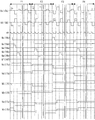
- It is a timing chart which shows the drive method of a liquid crystal display device provided with the liquid crystal panel 5a.
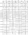
- It is a schematic diagram which shows the display state for every flame
- FIG. 16 is a schematic diagram illustrating a display state for each frame when the driving method of FIG. 15 is used.
- FIG. 20 is a timing chart showing a method for driving the gate driver of FIG. 19.
- FIG. It is a circuit diagram which shows the other structure of the gate driver which drives liquid crystal panel 5a * 5b.
- FIG. 20 is a timing chart which shows the drive method of the gate driver of FIG.
- It is a top view which shows the other structure of the liquid crystal panel 5a.
- It is a circuit diagram which shows the structure of the liquid crystal panel 5c.
- FIG. 5c It is a top view which shows the structure of the liquid crystal panel 5c. It is sectional drawing which shows the specific example of the cross section of the dashed-two dotted line part of FIG. It is sectional drawing which shows the other specific example of the cross section shown by the dashed-two dotted line part of FIG. It is a top view which shows the other structure of the liquid crystal panel 5c. It is a top view which shows other structure of the liquid crystal panel 5c. It is a timing chart which shows the drive method of a liquid crystal display device provided with the liquid crystal panel 5c. It is a schematic diagram which shows the display state of each period at the time of using the drive method of FIG. It is a circuit diagram which shows the structure of the gate driver which drives the liquid crystal panel 5c.
- FIG. 33 is a timing chart showing a method for driving the gate driver of FIG. 32.
- FIG. It is a circuit diagram which shows the structure of the liquid crystal panel 5d. It is a top view which shows the structure of the liquid crystal panel 5d. It is a circuit diagram which shows the structure of the liquid crystal panel 5e. It is a top view which shows the structure of the liquid crystal panel 5e. It is a timing chart which shows the drive method of a liquid crystal display device provided with the liquid crystal panel 5e. It is a schematic diagram which shows the display state of each period at the time of using the drive method of FIG. It is a circuit diagram which shows the further another structure of the liquid crystal panel 5a. It is a circuit diagram which shows the further another structure of the liquid crystal panel 5b.
- FIG. 10 is a circuit diagram showing still another configuration of a source driver. It is a block diagram explaining the whole structure of this liquid crystal display device. It is a block diagram explaining the function of this liquid crystal display device.
- FIG. 26 is a block diagram illustrating functions of the present television receiver. It is a disassembled perspective view which shows the structure of this television receiver. It is a top view which shows one structural example in case the liquid crystal panel 5a is made into a MVA system.
- FIG. 10 is a plan view showing still another configuration example of the liquid crystal panel according to the third exemplary embodiment.
- FIG. 10 is a plan view showing still another configuration example of the liquid crystal panel according to the third exemplary embodiment.
- FIG. 10 is a plan view showing still another configuration example of the liquid crystal panel according to the third exemplary embodiment.
- 12 is a plan view showing still another configuration example of the liquid crystal panel according to Embodiment 2.
- FIG. 10 is a plan view showing still another configuration example of the liquid crystal panel according to the third exemplary embodiment.
- FIG. 10 is a plan view showing still another configuration example of the liquid crystal panel according to the third exemplary embodiment.
- FIG. 10 is a plan view showing still another configuration example of the liquid crystal panel according to the fifth exemplary embodiment.
- 12 is a plan view showing still another configuration example of the liquid crystal panel according to Embodiment 2.
- FIG. It is a top view which shows the structure of the conventional liquid crystal panel.
- Liquid crystal panels 11a, 11b, 41A, 41B Contact holes 12a to 12f, 12A to 12F Transistors 15x 15X Data signal lines 16a to 16f 16p to 16s Scan signal lines 17a to 17f Pixel electrodes 17A to 17F Pixel electrodes 18x to 18z Holding Capacitance wiring 21 Organic gate insulating film 22 Inorganic gate insulating film 24 Semiconductor layer 25 Inorganic interlayer insulating film 26 Organic interlayer insulating film 37a / 37b / 37A / 37B Coupling capacitive electrode 67a / 67b / 67A / 67B Retention capacitive electrode 77a / 77b / 77A 77B contact electrode 84 liquid crystal display unit 100/101 pixel 601 television receiver 800 liquid crystal display device C100 / C101 coupling capacitance
- the extending direction of the scanning signal lines is hereinafter referred to as the row direction.
- the scanning signal line may extend in the horizontal direction or in the vertical direction. Needless to say.
- FIG. 1 is an equivalent circuit diagram showing a part of the liquid crystal panel.
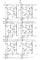
- the liquid crystal panel 5a includes data signal lines (15x and 15X) extending in the column direction (up and down direction in the figure) and scanning signal lines (16a to 16f) extending in the row direction (left and right direction in the figure).
- Pixels (100 to 105) arranged in the row and column directions, storage capacitor lines (18x to 18z), and a common electrode (counter electrode) com, and the structure of each pixel included in the odd-numbered pixel column is
- the structure of each pixel included in the even-numbered pixel column is the same, but the structure of each pixel included in the odd-numbered pixel column is different from the structure of each pixel included in the even-numbered pixel column. ing. Note that a pixel column including the pixels 100 to 102 and a pixel column including the pixels 103 to 105 are adjacent to each other.
- one data signal line and two scanning signal lines are provided corresponding to one pixel, and two pixel electrodes 17 c and 17 d provided in the pixel 100 and a pixel 101 are provided.
- the two pixel electrodes 17 a and 17 b provided in the pixel 102 and the two pixel electrodes 17 e and 17 f provided in the pixel 102 are arranged in a line, and the two pixel electrodes 17 C and 17 D provided in the pixel 103 are provided in the pixel 104.
- the two pixel electrodes 17A and 17B and the two pixel electrodes 17E and 17F provided in the pixel 105 are arranged in a line, the pixel electrodes 17c and 17C, the pixel electrodes 17d and 17D, the pixel electrodes 17a and 17A, and the pixel electrode 17b and 17B, pixel electrodes 17e and 17E, and pixel electrodes 17f and 17F are adjacent to each other in the row direction.
- the pixel electrodes 17c and 17d are connected via the coupling capacitor C100, the pixel electrode 17c is connected to the data signal line 15x via the transistor 12c connected to the scanning signal line 16c, and the pixel electrode 17d is Connected to the data signal line 15x through the transistor 12d connected to the scanning signal line 16d, a storage capacitor Chc is formed between the pixel electrode 17c and the storage capacitor line 18y, and a storage capacitor is formed between the pixel electrode 17d and the storage capacitor line 18y. Chd is formed, a liquid crystal capacitor Clc is formed between the pixel electrode 17c and the common electrode com, and a liquid crystal capacitor Cld is formed between the pixel electrode 17d and the common electrode com.
- the pixel electrodes 17C and 17D are connected via the coupling capacitor C103, and the pixel electrode 17C is connected to the data signal line via the transistor 12D connected to the scanning signal line 16d.
- the pixel electrode 17D is connected to the data signal line 15X via the transistor 12C connected to the scanning signal line 16c, and the storage capacitor ChC is formed between the pixel electrode 17C and the storage capacitor line 18y.
- the storage capacitor ChD is formed between the pixel electrode 17C and the common electrode com, and the liquid crystal capacitor ClD is formed between the pixel electrode 17D and the common electrode com.
- the pixel electrodes 17a and 17b are connected via the coupling capacitor C101, and the pixel electrode 17a is connected to the data signal line via the transistor 12a connected to the scanning signal line 16a.
- the pixel electrode 17b is connected to the data signal line 15x via the transistor 12b connected to the scanning signal line 16b
- a storage capacitor Cha is formed between the pixel electrode 17a and the storage capacitor line 18x
- the pixel electrode A storage capacitor Chb is formed between the pixel electrode 17a and the common electrode com
- a liquid crystal capacitor Clb is formed between the pixel electrode 17b and the common electrode com.
- the pixel electrodes 17A and 17B are connected via the coupling capacitor C104, and the pixel electrode 17A is connected to the data signal line via the transistor 12B connected to the scanning signal line 16b.
- the pixel electrode 17B is connected to the data signal line 15X via the transistor 12A connected to the scanning signal line 16a
- the storage capacitor ChA is formed between the pixel electrode 17A and the storage capacitor line 18x
- the pixel electrode A storage capacitor ChB is formed between the pixel electrode 17A and the common electrode com
- a liquid crystal capacitor ClB is formed between the pixel electrode 17B and the common electrode com.
- the liquid crystal display device including the liquid crystal panel 5a for example, for two scanning signal lines corresponding to one pixel, one is selected in the front frame of two consecutive frames and the other is selected in the rear frame. Specifically, the scanning signal lines 16c, 16a, and 16e are sequentially selected in one of the two consecutive frames, and the scanning signal lines 16d, 16b, and 16f are sequentially selected on the other. Further, in the liquid crystal display device including the liquid crystal panel 5a, one may be selected in each frame of consecutive n (n is a plurality) frames, and the other may be selected in each frame of the next consecutive n frames.
- the scanning signal lines 16c, 16a, and 16e are sequentially selected in each frame of consecutive n (n is a plurality) frames, while the scanning signal lines 16d, 16b, and 16f are sequentially selected in each subsequent frame of n frames. May be selected sequentially.
- the pixel electrode 17a is connected to the data signal line 15x (via the transistor 12a), and the pixel electrode 17b is connected to the data signal line 15x (via the transistor 12a and the pixel electrode 17a).
- Co Cl + Ch
- C101 capacitance value C ⁇ and transistor 12a OFF
- the potential of the pixel electrode 17a is Va
- the potential of the pixel electrode 17b after the transistor 12a is turned off Va ⁇ (C ⁇ / (C ⁇ + Co))
- the subpixel including the pixel electrode 17a is a bright subpixel
- pixel electrode Subpixels including 17b are dark subpixels.
- the subpixel including the electrode 17b is a bright subpixel, and the subpixel including the pixel electrode 17a is a dark subpixel.
- one subpixel is a bright subpixel in one frame and a dark subpixel in another frame, so the same subpixel is always a bright subpixel or always a dark subpixel.
- the temporal integration value of the luminance can be made uniform in each sub-pixel, and the display quality can be improved.
- each of the two scanning signal lines corresponding to one pixel is connected.
- the polarity of the signal potential supplied to the pixel electrode is inverted every two consecutive frames.
- the scanning signal line 16a is selected in one of the two consecutive frames and the scanning signal line 16b is selected on the other, the polarity of the signal potential supplied to the pixel electrodes 17a and 17b is a unit of two frames. Is reversed (described later).
- one of two scanning signal lines corresponding to one pixel is selected in each of consecutive n (n is a plurality) frames, and the other is selected in each of subsequent n frames.
- N is an even number
- the polarity of the signal potential supplied to the pixel electrode connected to each of the two scanning signal lines is inverted in units of one frame.
- the scanning signal line 16a is selected in each frame of consecutive n (n is an even number) frame
- the scanning signal line 16b is selected in each frame of the next consecutive n frames
- the pixel electrodes 17a and 17b are selected.
- the polarity of the signal potential supplied to the signal is inverted in units of one frame.
- the number of frames (the total period thereof) equal to the number of frames (their total period) and the pixel electrode potential is a positive polarity and a dark subpixel and the pixel electrode potential is a negative polarity to the dark subpixel.
- the number of frames (the total period thereof) can be made equal, and a DC voltage is hardly applied to the liquid crystal layer of each sub-pixel (the sub-pixel is difficult to be burned in).
- the pixel electrode in the sub-pixel is connected to the data signal line (via a transistor) in a certain frame, and the data signal line (via a transistor and another pixel electrode) in another frame.
- a signal potential considering the pull-in voltage can be supplied to the pixel electrode in the frame connected to the data signal line, so that a DC voltage is hardly applied to the liquid crystal layer of the sub-pixel ( It is possible to prevent the subpixel from being burned in).
- each pixel of an active matrix liquid crystal display device when the gate on pulse signal supplied to the gate line (scanning signal line) falls (deactivates), it is connected to the pixel electrode among the conductive electrodes of the transistor Due to the parasitic capacitance between the electrode and the gate line, the potential of the pixel electrode written from the source line (data signal line) is drawn. That is, when the pixel is driven by alternating current, if the positive signal potential and the negative signal potential for a certain gradation are made symmetrical with respect to the counter potential (Vcom), the above phenomenon causes the positive signal potential to be written.
- Vcom counter potential
- the intermediate potential of the pixel potential when the pixel potential and the negative signal potential are written deviates from the counter potential, and a DC voltage is applied to the liquid crystal layer of the pixel (the temporal integration value of the pixel electrode potential deviates from the counter potential).
- a DC voltage to the liquid crystal layer causes pixel burn-in. Therefore, in general, the influence of the pull-in voltage is avoided by setting the positive and negative signal potentials for a certain gray scale in consideration of the pull-in voltage at the gray scale.
- two pixel electrodes arranged diagonally opposite to each other are the same for four pixel electrodes included in two pixels adjacent in the row direction (sharing two scanning signal lines). Since it is connected to the scanning signal line, in a frame in which one of two subpixels adjacent in the row direction is a bright subpixel, the other is a dark subpixel.
- display unevenness for example, horizontal stripe-shaped unevenness
- a rough feeling forggy feeling
- the polarity of the signal potential supplied to each data signal line (15x / 15X) is inverted every horizontal scanning period (1H), thereby pulling in the potential when the transistor is OFF between two adjacent pixels in the column direction.
- the direction is reversed, and flickering can be suppressed (described later).
- the potential at the time of turning off the transistor between two adjacent pixels in the row direction can be obtained.
- the retraction direction is reversed, and flickering can be suppressed (described later).
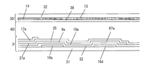
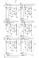
- FIG. 1 A specific example of the liquid crystal panel 5a is shown in FIG.
- the data signal line 15x is provided along the pixel 100 and the pixel 101
- the data signal line 15X is provided along the pixel 103 and the pixel 104
- the storage capacitor wiring 18y is connected to the pixels 100 and 103. Crossing the center of each pixel, the storage capacitor wiring 18x crosses the center of each of the pixels 101 and 104.
- the scanning signal line 16c is disposed so as to overlap with one of the two edge portions along the row direction of the pixel 100, and the scanning signal line 16d is disposed so as to overlap with the other.
- Pixel electrodes 17c and 17d are arranged in the column direction between 16c and 16d.
- the scanning signal line 16c overlaps one of the two edge portions along the row direction of the pixel 103, and the scanning signal line 16d overlaps the other, and the pixel between the scanning signal lines 16c and 16d is seen in plan view.
- Electrodes 17C and 17D are arranged in the column direction.
- the scanning signal line 16a is formed so as to overlap with one of the two edge portions along the row direction of the pixel 101, and the scanning signal line 16b is formed so as to overlap with the other, and the scanning signal line 16a is viewed in plan view.
- pixel electrodes 17a and 17b are arranged in the column direction. Further, the scanning signal line 16a overlaps one of the two edge portions along the row direction of the pixel 104, and the scanning signal line 16b overlaps the other, and the pixel between the scanning signal lines 16a and 16b is seen in plan view. Electrodes 17A and 17B are arranged in the column direction.
- the source electrode 8a and the drain electrode 9a of the transistor 12a are formed on the scanning signal line 16a, and the source electrode 8b and the drain electrode 9b of the transistor 12b are formed on the scanning signal line 16b.
- the source electrode 8a is connected to the data signal line 15x.
- the drain electrode 9a is connected to the drain lead wiring 27a, the drain lead wiring 27a is connected to the contact electrode 77a and the coupling capacitance electrode 37a, and the contact electrode 77a is connected to the pixel electrode 17a through the contact hole 11a and has a coupling capacitance.
- the electrode 37a overlaps with the pixel electrode 17b through an interlayer insulating film. As a result, a coupling capacitor C101 (see FIG.
- the source electrode 8b is connected to the data signal line 15x.
- the drain electrode 9b is connected to the drain lead wire 27b, the drain lead wire 27b is connected to the contact electrode 77b and the coupling capacitor electrode 37b, and the contact electrode 77b is connected to the pixel electrode 17b through the contact hole 11a and the coupling capacitor.
- the electrode 37b overlaps with the pixel electrode 17a through an interlayer insulating film.
- a coupling capacitor C101 (see FIG. 1) between the pixel electrodes 17a and 17b is formed at the overlapping portion of the coupling capacitor electrode 37b and the pixel electrode 17a.
- each of the coupling capacitor electrodes 37a and 37b overlaps the storage capacitor line 18x via the gate insulating film.
- the storage capacitor Cha (see FIG. 1) is formed at the overlapping portion of the coupling capacitor electrode 37a and the storage capacitor wire 18x
- the storage capacitor Chb (see FIG. 1) is formed at the overlapping portion of the coupling capacitor electrode 37b and the storage capacitor wire 18x. It is formed.
- the pixel electrodes 17a and 17b, the drain lead wires 27a and 27b, the contact electrodes 77a and 77b, the contact holes 11a and 11b, and the coupling capacitor electrodes 37a and 37b are connected to the scanning signal lines. It is provided in the pixel 101 so that the planar shape and the planar arrangement when viewed from the 16a side and the scanning signal line 16b side are the same. Further, the overlapping area of the drain electrode 9a and the drain lead wiring 27a and the scanning signal line 16a (parasitic capacitance Cgd between them) is the overlapping area of the drain electrode 9b and the drain leading wiring 27b and the scanning signal line 16b (between them). It is substantially equal to the parasitic capacitance Cgd).
- the pull-in voltage when the sub-pixel including the pixel electrode 17a becomes a bright sub-pixel is aligned with the pull-in voltage when the sub-pixel including the pixel electrode 17b becomes a bright sub-pixel. It is possible to reduce the risk that bright subpixels are burned out due to the above.
- two coupling capacitance electrodes (37a and 37b) are provided to parallelize the coupling capacitance. Therefore, even if the drain lead-out wiring 27a is disconnected at the tip portion (between the contact hole 11a and the coupling capacitor electrode 37a), the pixel 101 is driven with a frame in which the scanning signal lines 16a and 16b are selected (bright / dark). Pixel formation). Further, even if the drain lead-out wiring 27a is disconnected at the root portion (between the contact hole 11a and the drain electrode 9a), the pixel 101 is driven in the frame in which the scanning signal line 16b is selected (formation of light / dark subpixels). Is possible.
- the scanning signal line 16a can be obtained by cutting (correcting cutting) the drain lead-out wiring 27a at the tip (for example, below the gap between the pixel electrodes 17a and 17b). It becomes possible to drive the pixel 101 in a frame in which each of the 16b is selected (formation of bright / dark subpixels), and the pixel 101 is not used in the frame in which the scanning signal line 16b is selected without being cut. It is possible to drive completely (bright subpixel and black subpixel are formed).
- the pixel 104 can be driven (formation of bright / dark subpixels) in the frame in which the scanning signal line 16B is selected. Further, even if the pixel electrode 17A and the coupling capacitor electrode 37A are short-circuited, the pixel 104 can be driven incompletely (the entire pixel becomes a bright subpixel). Further, even if the storage capacitor line 18x and the contact electrode 77A are short-circuited, the pixel 104 can be driven incompletely in the frame in which the scanning signal line 16b is selected (a bright subpixel and a black subpixel are formed). ) Note that the configuration of the pixel 100 (the shape, arrangement, and connection relationship of each member) is the same as that of the pixel 101.
- the source electrode 8A and the drain electrode 9A of the transistor 12A are formed on the scanning signal line 16a, and the source electrode 8B and the drain electrode 9B of the transistor 12B are formed on the scanning signal line 16b.
- the source electrode 8A is connected to the data signal line 15X
- the drain electrode 9A is connected to the drain lead wire 27A
- the drain lead wire 27A is connected to the coupling capacitor electrode 37A and the contact electrode 77A
- the contact electrode 77A is the contact hole 11A.
- the coupling capacitor electrode 37A overlaps with the pixel electrode 17A via an interlayer insulating film, thereby forming a coupling capacitor C104 (see FIG. 1) between the pixel electrodes 17A and 17B. Is done.
- the source electrode 8B is connected to the data signal line 15X.
- the drain electrode 9B is connected to the drain lead wiring 27B.
- the drain lead wiring 27B is connected to the coupling capacitor electrode 37B and the contact electrode 77B.
- the contact electrode 77B is connected to the pixel electrode 17A via the contact hole 11B and coupled.
- the capacitor electrode 37B overlaps with the pixel electrode 17B via an interlayer insulating film, thereby forming a coupling capacitor C104 (see FIG. 1) between the pixel electrodes 17A and 17B.
- each of the contact electrodes 77A and 77B overlaps with the storage capacitor wiring 18x through the gate insulating film, thereby forming storage capacitors ChA and ChB.
- the pixel electrodes 17A and 17B, the drain lead wires 27A and 27B, the contact electrodes 77A and 77B, the contact holes 11A and 11B, and the coupling capacitor electrodes 37A and 37B are formed as scanning signal lines. It is provided in the pixel 104 so that the planar shape and the planar arrangement when viewed from the 16a side and the scanning signal line 16b side are the same.
- the overlapping area (parasitic capacitance Cgd) between the drain electrode 9A and the drain lead line 27A and the scanning signal line 16a is equal to the overlapping area between the drain electrode 9B and the drain lead line 27B and the scanning signal line 16b (between them). It is substantially equal to the parasitic capacitance Cgd).
- the pull-in voltage when the sub-pixel including the pixel electrode 17a becomes a bright sub-pixel is aligned with the pull-in voltage when the sub-pixel including the pixel electrode 17b becomes a bright sub-pixel. It is possible to reduce the risk that bright subpixels are burned out due to the above.
- the configuration of the pixel 103 (the shape, arrangement, and connection relationship of each member) is the same as that of the pixel 104.
- FIG. 3 is a cross-sectional view taken along the line AB of FIG.
- the liquid crystal panel 5a includes an active matrix substrate 3, a color filter substrate 30 facing the active matrix substrate 3, and a liquid crystal layer 40 disposed between the substrates (3, 30).
- the scanning signal line 16a and the storage capacitor wiring 18x are formed on the glass substrate 31, and the inorganic gate insulating film 22 is formed so as to cover them.
- a semiconductor layer 24 i layer and n + layer
- a source electrode 8a in contact with the n + layer a drain electrode 9a, drain lead wires 27a and 27b, a contact electrode 77a, and a coupling capacitor electrode 37a are formed.
- An inorganic interlayer insulating film 25 is formed so as to cover them.
- Pixel electrodes 17a and 17b are formed on the inorganic interlayer insulating film 25, and an alignment film (not shown) is formed so as to cover these (pixel electrodes 17a and 17b).
- the inorganic interlayer insulating film 25 is penetrated, whereby the pixel electrode 17a and the contact electrode 77a are connected.
- the coupling capacitor electrode 37a connected to the drain lead wiring 27a overlaps the pixel electrode 17b through the inorganic interlayer insulating film 25, thereby forming the coupling capacitor C101 (see FIG. 1).
- the coupling capacitor electrode 37a overlaps the storage capacitor wiring 18x via the inorganic gate insulating film 22, thereby forming the storage capacitor Cha (see FIG. 1).
- the black matrix 13 and the colored layer 14 are formed on the glass substrate 32, the common electrode (com) 28 is formed thereon, and an alignment film (not shown) is formed so as to cover this. Is formed.
- FIG. 49 shows a configuration in which the liquid crystal panel of FIG. 2 is an MVA (multi-domain vertical alignment) system.
- MVA multi-domain vertical alignment
- each pixel electrode of the active matrix substrate is provided with an alignment regulating slit SL
- the color regulating substrate has an alignment regulating rib (linear protrusion) Li.
- a slit for regulating the orientation can be provided in the common electrode of the color filter substrate.
- FIG. 3 can be configured as shown in FIG. That is, a thick organic gate insulating film 21 and a thin inorganic gate insulating film 22 are formed on the substrate, and a thin inorganic interlayer insulating film 25 and a thick organic interlayer insulating film 26 are formed below the pixel electrode. By doing so, the effects of reducing various parasitic capacitances and preventing short-circuiting between wirings can be obtained.
- the portion of the organic gate insulating film 21 located under the coupling capacitance electrode 37a is penetrated, and the portion of the organic interlayer insulating film 26 located on the coupling capacitance electrode is penetrated. It is preferable to pass through. In this way, the capacitance value of the coupling capacitor C101 and the capacitance value of the holding capacitor Cha can be increased.
- the inorganic interlayer insulation film 25, the organic interlayer insulation film 26, and the contact hole 11a of FIG. 4 can be formed as follows, for example. That is, after forming a transistor (TFT), an inorganic interlayer insulating film 25 (SiNx) having a thickness of about 3000 mm so as to cover the entire surface of the substrate using a mixed gas of SiH 4 gas, NH 3 gas, and N 2 gas. A passivation film) is formed by CVD. Thereafter, an organic interlayer insulating film 26 made of a positive photosensitive acrylic resin having a thickness of about 3 ⁇ m is formed by spin coating or die coating.
- TFT transistor
- SiNx inorganic interlayer insulating film 25
- SiNx inorganic interlayer insulating film 25 having a thickness of about 3000 mm so as to cover the entire surface of the substrate using a mixed gas of SiH 4 gas, NH 3 gas, and N 2 gas.
- a passivation film is formed by CVD.
- the organic gate insulating film 21 and the organic interlayer insulating film 26 may be, for example, an insulating film made of a SOG (spin-on glass) material, and the organic gate insulating film 21 and the organic interlayer insulating film 26 are made of acrylic resin. , At least one of an epoxy resin, a polyimide resin, a polyurethane resin, a novolac resin, and a siloxane resin may be contained.
- FIG. 5 Another specific example of the liquid crystal panel 5a is shown in FIG.
- the data signal line 15x is provided along the pixel 100 and the pixel 101
- the data signal line 15X is provided along the pixel 103 and the pixel 104
- the storage capacitor wiring 18y is provided in the pixels 100 and 103. Crossing the center of each pixel, the storage capacitor wiring 18x crosses the center of each of the pixels 101 and 104.
- the scanning signal line 16c is disposed so as to overlap with one of the two edge portions along the row direction of the pixel 100, and the scanning signal line 16d is disposed so as to overlap with the other.
- a pixel electrode 17c is disposed between 16c and the storage capacitor line 18y, and a pixel electrode 17d is disposed between the scanning signal line 16d and the storage capacitor line 18y.
- the scanning signal line 16c overlaps one of the two edge portions along the row direction of the pixel 103, and the scanning signal line 16d overlaps the other, and the scanning signal line 16c and the storage capacitor line 18y are seen in plan view.
- a pixel electrode 17C is disposed therebetween, and a pixel electrode 17D is disposed between the scanning signal line 16d and the storage capacitor wiring 18y.
- the scanning signal line 16a is formed so as to overlap with one of the two edge portions along the row direction of the pixel 101, and the scanning signal line 16b is formed so as to overlap with the other, and the scanning signal line 16a is viewed in plan view.
- a pixel electrode 17a is disposed between the storage capacitor line 18x and a pixel electrode 17b is disposed between the scanning signal line 16b and the storage capacitor line 18x.
- the scanning signal line 16a overlaps one of the two edge portions along the row direction of the pixel 104, and the scanning signal line 16b overlaps the other, and the scanning signal line 16a and the storage capacitor wiring 18x are seen in plan view.
- a pixel electrode 17A is disposed therebetween, and a pixel electrode 17B is disposed between the scanning signal line 16b and the storage capacitor line 18x.
- the source electrode 8a of the transistor 12a and the two drain electrodes 9a and 10a are formed on the scanning signal line 16a, and the source electrode 8b and the two drain electrodes 9b and 10b of the transistor 12b are formed on the scanning signal line 16b. Is formed.
- the source electrode 8a is connected to the data signal line 15x.
- the drain electrode 9a is connected to the contact electrode 77a via the drain lead wiring 27a, the contact electrode 77a is connected to the pixel electrode 17a via the contact hole 11a, and the drain electrode 10a is connected to the coupling capacitance electrode 37a via the drain lead wiring 19a. Furthermore, the coupling capacitor electrode 37a overlaps the pixel electrode 17b with an interlayer insulating film interposed therebetween.
- a coupling capacitor C101 (see FIG. 1) between the pixel electrodes 17a and 17b is formed at the overlapping portion of the coupling capacitor electrode 37a and the pixel electrode 17b.
- the drain lead wiring 19a is arranged between the pixel electrode 17a and the data signal line 15x in plan view.
- the source electrode 8b is connected to the data signal line 15x.
- the drain electrode 9b is connected to the contact electrode 77b via the drain lead wiring 27b, the contact electrode 77b is connected to the pixel electrode 17b via the contact hole 11b, and the drain electrode 10b is connected to the coupling capacitance electrode 37b via the drain lead wiring 19b.
- the coupling capacitor electrode 37b is overlapped with the pixel electrode 17a through an interlayer insulating film.
- a coupling capacitor C101 (see FIG. 1) between the pixel electrodes 17a and 17b is formed at the overlapping portion of the coupling capacitor electrode 37b and the pixel electrode 17a.
- the drain lead wiring 19b is disposed between the pixel electrode 17b and the data signal line 15X in plan view.
- a storage capacitor electrode 67a is disposed on the storage capacitor line 18x through a gate insulating film, and the storage capacitor electrode 67a and the pixel electrode 17a are connected through a contact hole 41a.
- a capacitor Cha (see FIG. 1) is formed.
- a storage capacitor electrode 67b is disposed on the storage capacitor line 18x through a gate insulating film, and the storage capacitor electrode 67b and the pixel electrode 17b are connected through a contact hole 41b.
- a capacitor Chb (see FIG. 1) is formed.
- the coupling capacitor electrodes 37a and 37b are provided in the pixel 101 so that the planar shape and the planar arrangement when viewed from the scanning signal line 16a side and the scanning signal line 16b side are the same.
- the overlapping area of the drain electrode 9a and the drain lead wirings 19a and 27a and the scanning signal line 16a is the overlapping area of the drain electrode 9b and the drain leading wirings 19b and 27b and the scanning signal line 16b. It is substantially equal to (parasitic capacitance Cgd between the two).
- the pull-in voltage when the sub-pixel including the pixel electrode 17a becomes a bright sub-pixel is aligned with the pull-in voltage when the sub-pixel including the pixel electrode 17b becomes a bright sub-pixel. It is possible to reduce the risk that bright subpixels are burned out due to the above.
- the configuration of the pixel 100 (the shape, arrangement, and connection relationship of each member) is the same as that of the pixel 101.
- a source electrode 8A and two drain electrodes 9A and 10A of the transistor 12A are formed on the scanning signal line 16a, and a source electrode 8B and two drain electrodes 9B and 10B of the transistor 12B are formed on the scanning signal line 16b. Is formed.
- the source electrode 8A is connected to the data signal line 15X.
- the drain electrode 10A is connected to the contact electrode 77A via the drain lead wiring 27A, the contact electrode 77A is connected to the pixel electrode 17B via the contact hole 11A, and the drain electrode 9A is connected to the coupling capacitance electrode 37A via the drain lead wiring 19A.
- the coupling capacitor electrode 37A overlaps the pixel electrode 17A via the interlayer insulating film, thereby forming a coupling capacitor C104 (see FIG. 1) between the pixel electrodes 17A and 17B.
- the drain lead wiring 27A is disposed between the pixel electrode 17A and the data signal line 15X in plan view.
- the source electrode 8B is connected to the data signal line 15X.
- the drain electrode 10B is connected to the contact electrode 77B via the drain lead wiring 27B, the contact electrode 77B is connected to the pixel electrode 17A via the contact hole 11B, and the drain electrode 9B is connected to the coupling capacitance electrode 37B via the drain lead wiring 19B.
- the coupling capacitor electrode 37B overlaps the pixel electrode 17B via the interlayer insulating film, thereby forming a coupling capacitor C104 (see FIG. 1) between the pixel electrodes 17A and 17B.
- the drain lead wiring 19B is arranged between the pixel electrode 17B and the data signal line adjacent to the right side of the data signal line 15X in plan view.
- a storage capacitor electrode 67A is disposed on the storage capacitor line 18x via a gate insulating film, and the storage capacitor electrode 67A and the pixel electrode 17A are connected through a contact hole 41A.
- a capacitor ChA (see FIG. 1) is formed.
- a storage capacitor electrode 67B is disposed on the storage capacitor line 18x via a gate insulating film, and the storage capacitor electrode 67B and the pixel electrode 17B are connected through a contact hole 41B.
- a capacitor ChB (see FIG. 1) is formed.
- the coupling capacitor electrodes 37A and 37B are provided in the pixel 104 so that the planar shape and the planar arrangement when viewed from the scanning signal line 16a side and the scanning signal line 16b side are the same.
- the overlapping area of the drain electrode 9A and the drain lead lines 19A and 27A and the scanning signal line 16a is the overlapping area of the drain electrode 9B and the drain lead lines 19B and 27B and the scanning signal line 16b. It is substantially equal to (parasitic capacitance Cgd between the two).
- the pull-in voltage when the sub-pixel including the pixel electrode 17a becomes a bright sub-pixel is aligned with the pull-in voltage when the sub-pixel including the pixel electrode 17b becomes a bright sub-pixel. It is possible to reduce the risk that bright subpixels are burned out due to the above.
- the configuration of the pixel 103 (the shape, arrangement, and connection relationship of each member) is the same as that of the pixel 104. Further, in the liquid crystal panel 5a of FIG. 5, since the drain lead-out wirings 19a, 19b, 27A, and 27B do not overlap the pixel electrode, the coupling capacitance value is increased while using a relatively thin interlayer insulating film as shown in FIG. It is suitable when it is made not to pass too much.
- FIG. 23 shows still another specific example of the liquid crystal panel 5a.
- the pixel arrangement, data signal lines, and scanning signal lines in the liquid crystal panel of FIG. 23 are the same as those of the liquid crystal panel of FIG.
- the source electrode 8a and the drain electrode 9a of the transistor 12a are formed on the scanning signal line 16a, and the source electrode 8b and the drain electrode 9b of the transistor 12b are formed on the scanning signal line 16b. Is formed.
- the source electrode 8a is connected to the data signal line 15x.
- the drain electrode 9a is connected to the contact electrode 77a through the drain lead wiring 27a, the contact electrode 77a is connected to the pixel electrode 17a through the contact hole 11a, and the pixel electrode 17a is connected to the storage capacitor electrode 67a through the contact hole 41a.
- the storage capacitor electrode 67a is connected to the coupling capacitor electrode 37, and the coupling capacitor electrode 37 overlaps the pixel electrode 17b via the interlayer insulating film, whereby the coupling capacitor C101 between the pixel electrodes 17a and 17b (FIG. 1) is formed.
- the source electrode 8b is connected to the data signal line 15x.
- the drain electrode 9b is connected to the contact electrode 77b via the drain lead wiring 27b, the contact electrode 77b is connected to the pixel electrode 17b via the contact hole 11b, and the pixel electrode 17b is connected to the storage capacitor electrode 67b via the contact hole 41b. Has been.
- Each of the storage capacitor electrodes 67a and 67b overlaps the storage capacitor wiring 18x via the gate insulating film, thereby forming the storage capacitors Cha and Chb (see FIG. 1). Note that the configuration of the pixel 100 (the shape, arrangement, and connection relationship of each member) is the same as that of the pixel 101.
- a source electrode 8A and two drain electrodes 9A and 10A of the transistor 12A are formed on the scanning signal line 16a, and a source electrode 8B and two drain electrodes 9B and 10B of the transistor 12B are formed on the scanning signal line 16b. Is formed.
- the source electrode 8A is connected to the data signal line 15X.
- the drain electrode 10A is connected to the contact electrode 77A via the drain lead wiring 27A, the contact electrode 77A is connected to the pixel electrode 17B via the contact hole 11A, and the drain electrode 9A is connected to the coupling capacitance electrode 37A via the drain lead wiring 19A.
- the coupling capacitor electrode 37A overlaps the pixel electrode 17A via the interlayer insulating film, thereby forming a coupling capacitor C104 (see FIG. 1) between the pixel electrodes 17A and 17B.
- the drain lead wiring 27A is disposed between the pixel electrode 17A and the data signal line 15X in plan view.
- the source electrode 8B is connected to the data signal line 15X.
- the drain electrode 10B is connected to the contact electrode 77B via the drain lead wiring 27B, the contact electrode 77B is connected to the pixel electrode 17A via the contact hole 11B, and the drain electrode 9B is connected to the coupling capacitance electrode 37B via the drain lead wiring 19B.
- the coupling capacitor electrode 37B overlaps the pixel electrode 17B via the interlayer insulating film, thereby forming a coupling capacitor C104 (see FIG. 1) between the pixel electrodes 17A and 17B.
- the drain lead wiring 19B is arranged between the pixel electrode 17B and the data signal line adjacent to the right side of the data signal line 15X in plan view.
- a storage capacitor electrode 67A is disposed on the storage capacitor line 18x via a gate insulating film, and the storage capacitor electrode 67A is connected to the drain lead-out line 27B, whereby the storage capacitor ChA (see FIG. 1). Is formed.
- a storage capacitor electrode 67B is disposed on the storage capacitor line 18x via a gate insulating film, and the storage capacitor electrode 67B is connected to the drain lead-out line 27A, whereby the storage capacitor ChB (see FIG. 1). Is formed. Note that the configuration of the pixel 103 (the shape, arrangement, and connection relationship of each member) is the same as that of the pixel 104.
- the storage capacitor wiring (18x to 18z) can be removed from the liquid crystal panel 5a, and in this case, the configuration is as shown in FIG. This configuration is advantageous in terms of the aperture ratio because there is no light-shielding storage capacitor wiring.
- FIG. 6 is a timing chart showing a driving method of the present liquid crystal display device (normally black mode liquid crystal display device) provided with the liquid crystal panel shown in FIGS. SV and sv indicate signal potentials supplied to two adjacent data signal lines (for example, 15x and 15X), and Ga to Gf are gate-on pulse signals supplied to the scanning signal lines 16a to 16f.
- Vc, Vd, Va, Vb, VC, and VD represent the potentials of the pixel electrodes 17c, 17d, 17a, 17b, 17C, and 17D, respectively, and sh represents a charge share signal.
- H charge share period
- all the data signal lines are short-circuited to each other or the same potential is supplied to all the data signal lines from the outside. Done.
- two scanning signal lines corresponding to one pixel are alternately selected in units of one frame, and the polarity of the signal potential supplied to the data signal line is set to one horizontal scanning period ( 1H), the polarity of the signal potential supplied in the same horizontal scanning period in each frame is inverted in units of two frames, and the two adjacent data signal lines are reversed in the same horizontal scanning period.
- a polarity signal potential is supplied, and charge sharing is performed at the beginning of each horizontal scanning period.
- the upper side (for example, the scanning signal lines 16c, 16a, and 16e) of the upper and lower scanning signal lines (see FIG. 1) corresponding to one pixel is set.
- a signal potential having a positive polarity is supplied to one of the two adjacent data signal lines (for example, the data signal line 15x) during the first horizontal scanning period (for example, including the writing period of the pixel electrode 17c).
- a negative-polarity signal potential is supplied in the second horizontal scanning period (for example, including the writing period of the pixel electrode 17a), and a positive-polarity signal is supplied in the third horizontal scanning period (for example, including the writing period of the pixel electrode 17e).
- a potential is supplied, and the other of the two data signal lines (for example, the data signal line 15X) has a first horizontal scanning period (for example, includes a writing period of the pixel electrode 17C).
- a negative-polarity signal potential is supplied, a positive-polarity signal potential is supplied during the second horizontal scanning period (for example, including the writing period of the pixel electrode 17A), and a third horizontal scanning period (for example, writing of the pixel electrode 17E) is performed.
- a negative polarity signal potential is supplied during the period of time. Accordingly, as shown in FIG.
- the sub-pixel including the pixel electrode 17c (plus polarity) is a bright sub-pixel (hereinafter “bright”)
- the sub-pixel including the pixel electrode 17d (plus polarity) is a dark sub-pixel (hereinafter referred to as “sub-pixel”).
- “Dark”) the subpixel including the pixel electrode 17C (minus polarity) is “dark”
- the subpixel including the pixel electrode 17D (minus polarity) is “bright”
- the subpixel including the pixel electrode 17a (minus polarity) is The sub-pixel including “bright” and the pixel electrode 17b (negative polarity) is “dark”, and the whole is as shown in FIG.
- the lower side (for example, scanning signal lines 16d, 16b, and 16f) is selected from the upper and lower scanning signal lines corresponding to one pixel, and one of the adjacent two data signal lines (for example, A positive polarity signal potential is supplied to the data signal line 15x) in the first horizontal scanning period (for example, including the writing period of the pixel electrode 17d), and the second horizontal scanning period (for example, the writing period of the pixel electrode 17b).
- a negative polarity signal potential, and a positive polarity signal potential is supplied during the third horizontal scanning period (for example, including the writing period of the pixel electrode 17f), and the other of the two data signal lines (for example, ,
- the signal potential of negative polarity is supplied to the data signal line 15X) in the first horizontal scanning period (for example, including the writing period of the pixel electrode 17D), and the second horizontal scanning period (for example, Supplying a signal electric potential of a negative polarity including a write-in period of the pixel electrode 17B), and supplies a signal electric potential of a positive polarity in the third horizontal scanning period (e.g., including the write-in period of the pixel electrode 17F). Accordingly, as shown in FIG.
- the sub-pixel including the pixel electrode 17c (positive polarity) is “dark”
- the sub-pixel including the pixel electrode 17d (positive polarity) is “bright”
- the pixel electrode 17C (negative polarity) is set.
- the pixel becomes “bright”, and the whole is as shown in FIG.
- the upper side (for example, the scanning signal lines 16c, 16a, and 16e) of the two upper and lower scanning signal lines corresponding to one pixel is selected, and one of the two adjacent data signal lines (for example, the data line)
- the signal line 15x) is supplied with a negative polarity signal potential in the first horizontal scanning period (for example, including the writing period of the pixel electrode 17c), and includes the second horizontal scanning period (for example, including the writing period of the pixel electrode 17a).
- a negative polarity signal potential is supplied during the third horizontal scanning period (for example, including the writing period of the pixel electrode 17e), and the other of the two data signal lines (for example, The data signal line 15X) is supplied with a positive polarity signal potential in the first horizontal scanning period (for example, including the writing period of the pixel electrode 17C), and is supplied in the second horizontal scanning period (for example, Supplying a signal electric potential of a positive polarity including a write-in period of the pixel electrode 17A), and supplies a signal electric potential of a negative polarity to the third horizontal scanning period (e.g., including the write-in period of the pixel electrode 17E). Accordingly, as shown in FIG.
- the subpixel including the pixel electrode 17c (minus polarity) is “bright”
- the subpixel including the pixel electrode 17d (minus polarity) is “dark”
- the pixel electrode 17C (plus polarity) is set.
- the sub-pixel including “dark”, the sub-pixel including the pixel electrode 17D (plus polarity) is “bright”
- the sub-pixel including the pixel electrode 17a (plus polarity) is “bright”
- the pixel is “dark”, and the whole is as shown in FIG.
- the lower side (for example, the scanning signal lines 16d, 16b, and 16f) of the two upper and lower scanning signal lines (see FIG. 1) corresponding to one pixel is selected, and two adjacent data signal lines are selected.
- One for example, the data signal line 15x
- the first horizontal scanning period for example, including the writing period of the pixel electrode 17d
- the second horizontal scanning period for example, the pixel
- the positive signal potential is supplied to the electrode 17b (including the writing period)
- the negative signal potential is supplied to the third horizontal scanning period (for example, the pixel electrode 17f includes the writing period), and the two data signals are supplied.
- the other of the lines (for example, the data signal line 15X) is supplied with a positive signal potential in the first horizontal scanning period (for example, including the writing period of the pixel electrode 17D), and the second horizontal scanning.
- a positive signal potential in the first horizontal scanning period for example, including the writing period of the pixel electrode 17D
- the second horizontal scanning e.g., including the write-in period of the pixel electrode 17B
- supplies a signal electric potential of a positive polarity supplies a signal electric potential of a negative polarity to the third horizontal scanning period (e.g., including the write-in period of the pixel electrode 17F).
- the subpixel including the pixel electrode 17c (minus polarity) is “dark”, the subpixel including the pixel electrode 17d (minus polarity) is “bright”, and the pixel electrode 17C (plus polarity) is set.
- the sub-pixel including “bright”, the sub-pixel including the pixel electrode 17D (plus polarity) is “dark”, the sub-pixel including the pixel electrode 17a (plus polarity) is “dark”, and the sub-pixel including the pixel electrode 17b (plus polarity).
- the pixel becomes “bright”, and the whole is as shown in FIG.
- the bright subpixels and the dark subpixels are arranged in a checkered pattern in each frame, and the bright subpixels and the dark subpixels can be exchanged in units of one frame. The quality can be improved.
- FIG. 50 is a timing chart showing another driving method of the present liquid crystal display device including the liquid crystal panel shown in FIGS.
- this driving method in one horizontal scanning period, first, a transistor connected to one pixel electrode in a state where a common electrode potential is supplied to two pixel electrodes provided in one pixel. Then, the signal potential is written to the other pixel electrode.
- the scanning signal line 16b is turned ON / OFF during the charge sharing period at the beginning of the horizontal scanning period of the scanning signal line 16a.
- the transistor 12b connected to the pixel electrode 17b can be turned off while the common electrode potential is supplied to the pixel electrodes 17a and 17b during the charge sharing period, and the pixel electrode 17b can be discharged at this time. . That is, in one horizontal scanning period, the pixel electrode 17b can be discharged first, and then the signal potential can be written to the pixel electrode 17a.
- the potential of the pixel electrode 17b (that is, the luminance of the dark subpixel) after the scanning signal line 16a is turned off is set to a desired value that is not affected by the signal potential written to the pixel electrode 17b one frame before. it can.
- discharge of one pixel electrode and writing of a signal potential to the other pixel electrode are performed within one horizontal scanning period, but the present invention is not limited to this.
- the discharge of one pixel electrode and the writing of the signal potential to the other pixel electrode may be performed in different horizontal scanning periods.
- the scanning signal lines 16a and 16b are synchronously turned ON / OFF during the charge sharing period of the horizontal scanning period, which is one previous (1H before) the horizontal scanning period of the scanning signal line 16a (this) Can also discharge the pixel electrode 17b). This may be performed before 2H or 3H.
- the pixel electrode can be discharged by so-called black insertion.
- the scanning signal lines 16a and 16b are turned on and off in synchronization with each other in the charge sharing period of each of a plurality of horizontal scanning periods that are about 1/3 V (vertical scanning period) before the horizontal scanning period of the scanning signal line 16a.
- 2 / 3V is a data display and black display is performed during a period of 1 / 3V, so that tailing or the like during moving image display can be suppressed.
- Discharge due to black insertion is preferably performed about 1 / 3V before writing of the signal potential, but 1 / 5V to 1 / 2V before writing (1 / 2V to 4 / 5V after writing). Just do it.
- FIG. 8 is a timing chart showing still another driving method of the present liquid crystal display device including the liquid crystal panel shown in FIGS.
- this driving method as shown in FIG. 8, for two scanning signal lines corresponding to one pixel, one of the two consecutive frames is selected, and the other of the two consecutive frames is the other.
- the polarity of the signal potential supplied to the data signal line is inverted every horizontal scanning period (1H), and the polarity of the signal potential supplied during the same horizontal scanning period in each frame is set in units of one frame.
- Inverted signal potentials may be supplied to two adjacent data signal lines in the same horizontal scanning period, and charge sharing may be performed at the beginning of each horizontal scanning period.
- the upper side (for example, the scanning signal lines 16c, 16a, and 16e) of the upper and lower scanning signal lines (see FIG. 1) corresponding to one pixel is set.
- a signal potential having a positive polarity is supplied to one of the two adjacent data signal lines (for example, the data signal line 15x) during the first horizontal scanning period (for example, including the writing period of the pixel electrode 17c).
- a negative-polarity signal potential is supplied in the second horizontal scanning period (for example, including the writing period of the pixel electrode 17a), and a positive-polarity signal is supplied in the third horizontal scanning period (for example, including the writing period of the pixel electrode 17e).
- a potential is supplied, and the other of the two data signal lines (for example, the data signal line 15X) has a first horizontal scanning period (for example, includes a writing period of the pixel electrode 17C).
- a negative-polarity signal potential is supplied, a positive-polarity signal potential is supplied during the second horizontal scanning period (for example, including the writing period of the pixel electrode 17A), and a third horizontal scanning period (for example, writing of the pixel electrode 17E) is performed.
- a negative polarity signal potential is supplied during the period of time.
- the sub-pixel including the pixel electrode 17c (plus polarity) is a bright sub-pixel (hereinafter “bright”)
- the sub-pixel including the pixel electrode 17d (plus polarity) is a dark sub-pixel (hereinafter referred to as “sub-pixel”).
- “Dark”) the subpixel including the pixel electrode 17C (minus polarity) is “dark”
- the subpixel including the pixel electrode 17D (minus polarity) is “bright”
- the subpixel including the pixel electrode 17a (minus polarity) is The sub-pixel including “bright” and the pixel electrode 17b (negative polarity) is “dark”, and as a whole, as shown in FIG.
- the upper side (for example, the scanning signal lines 16c, 16a, and 16e) is selected from the upper and lower scanning signal lines (see FIG. 1) corresponding to one pixel, and the two adjacent data signal lines are selected.
- a negative-polarity signal potential is supplied in the first horizontal scanning period (for example, including the writing period of the pixel electrode 17c), and the second horizontal scanning period (for example, the pixel electrode) 17a), a positive polarity signal potential is supplied, and a negative polarity signal potential is supplied in the third horizontal scanning period (eg, the pixel electrode 17e writing period), and the two data signal lines
- the other (for example, the data signal line 15X) is supplied with a positive signal potential in the first horizontal scanning period (for example, including the writing period of the pixel electrode 17C), and the second horizontal scanning.
- the subpixel including the pixel electrode 17c (minus polarity) is “bright”, the subpixel including the pixel electrode 17d (minus polarity) is “dark”, and the pixel electrode 17C (plus polarity) is set.
- the pixel is “dark”, and the whole is as shown in FIG.
- the lower side (for example, the scanning signal lines 16d, 16b, and 16f) of the two upper and lower scanning signal lines (see FIG. 1) corresponding to one pixel is selected, and two adjacent data signal lines are selected.
- One for example, the data signal line 15x
- the first horizontal scanning period for example, including the writing period of the pixel electrode 17c
- the second horizontal scanning period for example, the pixel
- the negative polarity signal potential is supplied to the electrode 17a (including the writing period)
- the positive polarity signal potential is supplied to the third horizontal scanning period (for example, the pixel electrode 17e includes the writing period), and the two data signals are supplied.
- the other of the lines (for example, the data signal line 15X) is supplied with a negative-polarity signal potential in the first horizontal scanning period (for example, including the writing period of the pixel electrode 17C), and the second horizontal scanning.
- a negative-polarity signal potential in the first horizontal scanning period for example, including the writing period of the pixel electrode 17C
- the second horizontal scanning e.g., including the write-in period of the pixel electrode 17A
- a positive polarity in the third horizontal scanning period e.g., including the write-in period of the pixel electrode 17E.
- the sub-pixel including the pixel electrode 17c (positive polarity) is “dark”
- the sub-pixel including the pixel electrode 17d (positive polarity) is “bright”
- the pixel electrode 17C (negative polarity) is set.
- the pixel becomes “bright”, and the whole is as shown in FIG.
- the lower side (for example, the scanning signal lines 16d, 16b, and 16f) of the two upper and lower scanning signal lines (see FIG. 1) corresponding to one pixel is selected, and two adjacent data signal lines are selected.
- One for example, the data signal line 15x
- the first horizontal scanning period for example, including the writing period of the pixel electrode 17c
- the second horizontal scanning period for example, the pixel
- the positive signal potential is supplied to the electrode 17a (including the writing period), and the negative signal potential is supplied to the third horizontal scanning period (for example, the pixel electrode 17e includes the writing period).
- the other of the lines (for example, the data signal line 15X) is supplied with a positive signal potential in the first horizontal scanning period (for example, including the writing period of the pixel electrode 17C), and the second horizontal scanning.
- a positive signal potential in the first horizontal scanning period for example, including the writing period of the pixel electrode 17C
- the second horizontal scanning During (e.g., including the write-in period of the pixel electrode 17A) supplies a signal electric potential of a positive polarity, and supplies a signal electric potential of a negative polarity to the third horizontal scanning period (e.g., including the write-in period of the pixel electrode 17E).
- the sub-pixel including the pixel electrode 17c (minus polarity) is “dark”, the sub-pixel including the pixel electrode 17d (minus polarity) is “bright”, and the pixel electrode 17C (plus polarity) is The sub-pixel including “bright”, the sub-pixel including the pixel electrode 17D (plus polarity) is “dark”, the sub-pixel including the pixel electrode 17a (plus polarity) is “dark”, and the sub-pixel including the pixel electrode 17b (plus polarity).
- the pixel becomes “bright”, and the whole is as shown in FIG.
- the bright subpixels and the dark subpixels are arranged in a checkered pattern in each frame, and the bright subpixels and the dark subpixels can be switched in units of two frames. The quality can be improved.
- FIG. 19 is a circuit diagram showing the configuration of the gate driver of the liquid crystal display device.
- the gate driver GD includes a shift register 45, a plurality of AND circuits (66a to 66f) arranged in the column direction, and an output circuit 46.
- the shift register 45 receives a gate star, a pulse signal GSP, and a gate clock signal GCK.
- the output of each stage of the shift register 45 is divided into two systems, one of which is input to the odd-numbered AND circuit, and the other is input to the even-numbered AND circuit adjacent thereto.
- the gate driver output control signal GOE is composed of two systems of signals (OEx ⁇ OEy).
- An inverted signal of the signal OEy is input to the odd-numbered AND circuit, and an inverted signal of the signal OEx is input to the even-numbered AND circuit.
- the output of one AND circuit becomes a gate-on pulse signal through the output circuit 46 and is supplied to one scanning signal line.
- the output from a certain stage of the shift register 45 is divided into two systems, one Qc of which is input to the AND circuit 66c, and the other Qd is input to the AND circuit 66d.
- the signal OEy is input to the AND circuit 66c
- the signal OEx is input to the AND circuit 66d.
- the output of the AND circuit 66c passes through the output circuit 46 to become a gate-on pulse signal Gc and is supplied to the scanning signal line 16c.
- the output of the AND circuit 66d becomes a gate-on pulse signal Gd through the output circuit 46, and is supplied to the scanning signal line 16d.
- the output from the other stage of the shift register 45 is divided into two systems, one of which Qa is input to the AND circuit 66a, and the other Qb is input to the AND circuit 66b. Further, the signal OEy is input to the AND circuit 66a, and the signal OEx is input to the AND circuit 66b.
- the output of the AND circuit 66a passes through the output circuit 46 and becomes a gate-on pulse signal Ga, which is supplied to the scanning signal line 16a. Further, the output of the AND circuit 66b becomes a gate-on pulse signal Gb through the output circuit 46, and is supplied to the scanning signal line 16b.
- FIG. 20 is a timing chart showing the operation of the gate driver of FIG.
- the signal OEx is always “H” in the odd-numbered frame and “H” in the rear end of each horizontal scanning period in the even-numbered frame, while the signal OEy is always “ “L”, in an odd frame, “H” at the rear end of each horizontal scanning period.
- the gate-on pulse signals Gc, Ga, and Ge are sequentially set to “H” (active) at intervals
- the gate-on pulse signals Gd, Gb, and Gf are set at intervals. Then, it can be sequentially set to “H” (active), and driving as shown in FIG. 6 is realized.
- the gate driver as shown in FIG.
- FIG. 21 is a timing chart showing the operation of the gate driver shown in FIG. 21.
- GOE is always “L” in odd frames and always “H” in even frames.
- the gate-on pulse signals Gc, Ga, and Ge are sequentially set to “H” (active) without an interval, and in the even frame, the gate-on pulse signals Gd, Gb, and Gf are Instead, it can be sequentially set to “H” (active), and driving as shown in FIG. 18 is realized. Note that the configuration of FIG.
- FIG. 19 has an advantage that the width of the gate-on pulse (write pulse) can be set as appropriate, and the configuration of FIG. 21 has an advantage that the GOE signal can be made into one system. Further, in the configuration of FIG. 19 or FIG. 21, a gate-on pulse signal to be supplied to each of two scanning signal lines corresponding to one pixel can be generated using an output from the same stage of one shift register. There is an advantage that the configuration can be simplified.
- the present liquid crystal panel can also be configured as shown in FIG.
- the liquid crystal panel 5b of FIG. 10 unlike the liquid crystal panel 5a of FIG. 1, all the pixels have the same structure. That is, in the liquid crystal panel 5a, for four pixel electrodes included in two pixels adjacent in the row direction (sharing two scanning signal lines), two pixel electrodes arranged diagonally opposite each other have the same scanning signal.
- two pixel electrodes arranged adjacent to each other in the row direction are connected to the same scanning signal line in the liquid crystal panel 5b.
- one data signal line and two scanning signal lines are provided corresponding to one pixel, and two pixel electrodes 17 c and 17 d provided in the pixel 100 and a pixel 101 are provided.
- the two pixel electrodes 17 a and 17 b provided in the pixel 102 and the two pixel electrodes 17 e and 17 f provided in the pixel 102 are arranged in a line, and the two pixel electrodes 17 C and 17 D provided in the pixel 103 are provided in the pixel 104.
- the two pixel electrodes 17A and 17B and the two pixel electrodes 17E and 17F provided in the pixel 105 are arranged in a line, the pixel electrodes 17c and 17C, the pixel electrodes 17d and 17D, the pixel electrodes 17a and 17A, and the pixel electrode 17b and 17B, pixel electrodes 17e and 17E, and pixel electrodes 17f and 17F are adjacent to each other in the row direction.
- the pixel electrodes 17a and 17b are connected via the coupling capacitor C101, the pixel electrode 17a is connected to the data signal line 15x via the transistor 12a connected to the scanning signal line 16a, and the pixel electrode 17b.
- a storage capacitor Cha is formed between the pixel electrode 17a and the storage capacitor line 18x, and between the pixel electrode 17b and the storage capacitor line 18x.
- a storage capacitor Chb is formed, a liquid crystal capacitor Cla is formed between the pixel electrode 17a and the common electrode com, and a liquid crystal capacitor Clb is formed between the pixel electrode 17b and the common electrode com.
- the pixel electrodes 17A and 17B are connected via the coupling capacitor C104, and the pixel electrode 17A is connected to the data signal line via the transistor 12A connected to the scanning signal line 16a.
- the pixel electrode 17B is connected to the data signal line 15X via the transistor 12B connected to the scanning signal line 16b
- a storage capacitor ChA is formed between the pixel electrode 17A and the storage capacitor line 18x
- the pixel electrode A storage capacitor ChB is formed between 17B and the storage capacitor line 18x
- a liquid crystal capacitor ClA is formed between the pixel electrode 17A and the common electrode com
- a liquid crystal capacitor ClB is formed between the pixel electrode 17B and the common electrode com.
- the driving method of the scanning signal lines (16a to 16f) and the data signal lines (15x and 15X) of the liquid crystal display device (liquid crystal display device in the normally black mode) provided with the liquid crystal panel 5b is the liquid crystal provided with the liquid crystal panel 5a It is the same as that of the display device.
- one sub-pixel is a bright sub-pixel in one frame and a dark sub-pixel in another frame, so that the same sub-pixel is always a bright sub-pixel or a dark sub-pixel.
- the temporal integration value of luminance can be made uniform in each sub-pixel, and the display quality can be improved.
- the other is a dark pixel, so that bright pixels are adjacent in the column direction or dark pixels are adjacent in the column direction.
- a rough feeling can be suppressed.
- the same subpixel is always a bright subpixel or is always a dark subpixel. Display unevenness (for example, horizontal stripe-shaped unevenness) and a rough feeling (jaggy feeling) can be suppressed.
- FIG. 11 A specific example of the liquid crystal panel 5b is shown in FIG. Note that the pixel arrangement, the data signal lines, and the scanning signal lines in the liquid crystal panel in FIG. 11 are the same as those in the liquid crystal panel in FIG. As shown in FIG. 11, in the pixel 101, the source electrode 8a and the drain electrode 9a of the transistor 12a are formed on the scanning signal line 16a, and the source electrode 8b and the drain electrode 9b of the transistor 12b are formed on the scanning signal line 16b. Is formed. The source electrode 8a is connected to the data signal line 15x.
- the drain electrode 9a is connected to the drain lead wiring 27a, the drain lead wiring 27a is connected to the contact electrode 77a and the coupling capacitance electrode 37a, and the contact electrode 77a is connected to the pixel electrode 17a through the contact hole 11a and has a coupling capacitance.
- the electrode 37a overlaps with the pixel electrode 17b through an interlayer insulating film.
- a coupling capacitor C101 (see FIG. 10) between the pixel electrodes 17a and 17b is formed at the overlapping portion of the coupling capacitor electrode 37a and the pixel electrode 17b.
- the source electrode 8b is connected to the data signal line 15x.
- the drain electrode 9b is connected to the drain lead wiring 27b, the drain lead wiring 27b is connected to the contact electrode 77b and the coupling capacitor electrode 37b, and the contact electrode 77b is connected to the pixel electrode 17b through the contact hole 11b and has a coupling capacitance.
- the electrode 37b overlaps with the pixel electrode 17a through an interlayer insulating film.
- a coupling capacitor C101 (see FIG. 10) between the pixel electrodes 17a and 17b is formed at the overlapping portion of the coupling capacitor electrode 37b and the pixel electrode 17a.
- each of the coupling capacitor electrodes 37a and 37b overlaps the storage capacitor line 18x via the gate insulating film.
- the storage capacitor Cha see FIG.
- the pixel electrodes 17a and 17b, the drain lead wires 27a and 27b, the contact electrodes 77a and 77b, the contact holes 11a and 11b, and the coupling capacitor electrodes 37a and 37b are connected to the scanning signal lines. It is provided in the pixel 101 so that the planar shape and the planar arrangement when viewed from the 16a side and the scanning signal line 16b side are the same. Further, the overlapping area of the drain electrode 9a and the drain lead wiring 27a and the scanning signal line 16a (parasitic capacitance Cgd between them) is the overlapping area of the drain electrode 9b and the drain leading wiring 27b and the scanning signal line 16b (between them). It is substantially equal to the parasitic capacitance Cgd).
- the pull-in voltage when the sub-pixel including the pixel electrode 17a becomes a bright sub-pixel is aligned with the pull-in voltage when the sub-pixel including the pixel electrode 17b becomes a bright sub-pixel. It is possible to reduce the risk that bright subpixels are burned out due to the above.
- the configuration of the pixel 100 (the shape, arrangement, and connection relationship of each member) is the same as that of the pixel 101.
- the source electrode 8A and the drain electrode 9A of the transistor 12A are formed on the scanning signal line 16a, and the source electrode 8B and the drain electrode 9B of the transistor 12B are formed on the scanning signal line 16b.
- the source electrode 8A is connected to the data signal line 15X.
- the drain electrode 9A is connected to the drain lead wiring 27A, the drain lead wiring 27A is connected to the contact electrode 77A and the coupling capacitor electrode 37A, and the contact electrode 77A is connected to the pixel electrode 17A via the contact hole 11A and the coupling capacitor.
- the electrode 37A overlaps the pixel electrode 17B via an interlayer insulating film, thereby forming a coupling capacitor C101 (see FIG. 10) between the pixel electrodes 17A and 17B.
- the source electrode 8B is connected to the data signal line 15X.
- the drain electrode 9B is connected to the drain lead wiring 27B
- the drain lead wiring 27B is connected to the contact electrode 77B and the coupling capacitor electrode 37B
- the contact electrode 77B is connected to the pixel electrode 17B via the contact hole 11B and the coupling capacitance.
- the electrode 37B overlaps with the pixel electrode 17A via an interlayer insulating film, thereby forming a coupling capacitor C101 (see FIG. 10) between the pixel electrodes 17A and 17B.
- each of the coupling capacitor electrodes 37A and 37B overlaps with the storage capacitor wiring 18x through the gate insulating film, thereby forming the storage capacitors ChA and ChB (see FIG. 1).
- the pixel electrodes 17A and 17B, the drain lead wires 27A and 27B, the contact electrodes 77A and 77B, the contact holes 11A and 11B, and the coupling capacitor electrodes 37A and 37B are connected to the scanning signal lines. It is provided in the pixel 104 so that the planar shape and the planar arrangement when viewed from the 16a side and the scanning signal line 16b side are the same.
- the overlapping area (parasitic capacitance Cgd) between the drain electrode 9A and the drain lead line 27A and the scanning signal line 16A is equal to the overlapping area between the drain electrode 9B and the drain lead line 27B and the scanning signal line 16B (between them). It is substantially equal to the parasitic capacitance Cgd).
- the pull-in voltage when the sub-pixel including the pixel electrode 17a becomes a bright sub-pixel is aligned with the pull-in voltage when the sub-pixel including the pixel electrode 17b becomes a bright sub-pixel. It is possible to reduce the risk that bright subpixels are burned out due to the above.
- the configuration of the pixel 103 (the shape, arrangement, and connection relationship of each member) is the same as that of the pixel 104.
- FIG. 12 shows still another specific example of the liquid crystal panel 5b.
- the pixel arrangement, data signal lines, and scanning signal lines in the liquid crystal panel of FIG. 12 are the same as those of the liquid crystal panel of FIG.
- the source electrode 8a and the drain electrode 9a of the transistor 12a are formed on the scanning signal line 16a
- the source electrode 8b and the drain electrode 9b of the transistor 12b are formed on the scanning signal line 16b. Is formed.
- the source electrode 8a is connected to the data signal line 15x.
- the drain electrode 9a is connected to the pixel electrode 17a through the drain lead-out wiring and the contact hole 11a, the pixel electrode 17a is connected to the storage capacitor electrode 67a through the contact hole 41a, and the storage capacitor electrode 67a is connected to the coupling capacitor electrode 37a. Further, the coupling capacitor electrode 37a overlaps the pixel electrode 17b with an interlayer insulating film interposed therebetween, whereby a coupling capacitor C101 (see FIG. 10) between the pixel electrodes 17a and 17b is formed.
- the source electrode 8b is connected to the data signal line 15x.
- the drain electrode 9b is connected to the pixel electrode 17b through the drain lead-out wiring and the contact hole 11b, the pixel electrode 17b is connected to the storage capacitor electrode 67b through the contact hole 41b, and the storage capacitor electrode 67b is connected to the coupling capacitor electrode 37b. Furthermore, the coupling capacitor electrode 37b overlaps the pixel electrode 17a with an interlayer insulating film interposed therebetween, whereby a coupling capacitor C101 (see FIG. 10) between the pixel electrodes 17a and 17b is formed.
- the coupling capacitor electrode 37b is disposed on the scanning signal line 16a side of the storage capacitor electrode 67b and overlaps with the pixel electrode 17a, and the coupling capacitor electrode 37a is disposed on the scanning signal line 16b side of the storage capacitor electrode 67a. Since the pixel electrode 17b overlaps with the pixel electrode 17b, there is an advantage that even if the alignment of the coupling capacitance electrodes 37a and 37b is shifted in the column direction, the value of the coupling capacitance is compensated between them.
- Each of the storage capacitor electrodes 67a and 67b overlaps the storage capacitor wiring 18x via the gate insulating film, thereby forming the storage capacitors Cha and Chb (see FIG. 10).
- the configuration of the pixels 100, 103, and 104 (the shape and arrangement of each member and the connection relationship) is the same as that of the pixel 101.
- FIG. 13 is a timing chart showing a driving method of the present liquid crystal display device (normally black mode liquid crystal display device) provided with the liquid crystal panel shown in FIGS. SV and sv indicate signal potentials supplied to two adjacent data signal lines (for example, 15x and 15X), and Ga to Gf are gate-on pulse signals supplied to the scanning signal lines 16a to 16f.
- Vc, Vd, Va, Vb, VC, and VD represent the potentials of the pixel electrodes 17c, 17d, 17a, 17b, 17C, and 17D, respectively, and sh represents a charge share signal.
- the driving method of the data signal lines (15x and 15X) and the scanning signal lines (16a to 16f) in each frame (F1 to F4) is the same as that of FIG.
- a display as shown in FIG. 14A is obtained, a display as shown in FIG. 14B is obtained at F2, a display as shown in FIG. 14C is obtained at F3, and a display as shown in FIG. 14D is obtained at F4. It is done.
- FIG. 15 is a timing chart showing another driving method of the present liquid crystal display device including the liquid crystal panel shown in FIGS.
- the driving method of the data signal lines (15x and 15X) and the scanning signal lines (16a to 16f) in each frame (F1 to F4) is the same as that of FIG.
- a display as shown in FIG. 16A is obtained, a display as shown in FIG. 16B is obtained at F2, a display as shown in FIG. 16C is obtained at F3, and a display as shown in FIG. 16D is obtained at F4. It is done.
- FIG. 55 shows still another configuration of the present embodiment.
- two scanning signal lines 16a and 16b corresponding to the pixel 101 are arranged at both ends of the pixel 101, and a storage capacitor wiring 18x is provided so as to cross the pixel.
- the pixel 101 has a pixel electrode 17b that is Z-shaped when viewed in the column direction (the extending direction of the data signal line 15x), and two pixel electrodes 17a and 17u that are arranged on both sides of the pixel electrode 17b so as to be fitted therewith.
- a coupling capacitor electrode 37a is provided so as to overlap the pixel electrode 17b with an interlayer insulating film interposed therebetween.
- the transistor 12a is formed on the scanning signal line 16a
- the transistor 12b is formed on the scanning signal line 16b
- the drain electrode of the transistor 12a is connected to the pixel electrode 17a via the drain lead wiring 27a and the contact hole 11a.
- the drain electrode of the transistor 12b is connected to the pixel electrode 17b through the contact hole 11b, and the source electrodes of the transistors Tr12a and 12b are connected to the data signal line 15x.
- the coupling capacitor electrode 37a (which overlaps the pixel electrode 17b via an interlayer insulating film) has a parallelogram shape, and connection wirings 119a and 119u are connected to both sides thereof. Further, the connection wiring 119a is connected to the pixel via the contact hole 11ai. Connected to the electrode 17a, the connecting wiring 119u is connected to the pixel electrode 17u through the contact hole 11ui. As a result, a coupling capacitance between the pixel electrodes 17a and 17u and the pixel electrode 17b is formed at an overlapping portion of the coupling capacitance electrode 37a and the pixel electrode 17b.
- the storage capacitor electrodes 67b and 67u are arranged in the row direction (extending direction of the scanning signal line) so as to overlap the storage capacitor wiring 18x through the gate insulating film, and the pixel electrode 17b is in contact with the pixel 101.
- the pixel electrode 17u is connected to the storage capacitor electrode 67u through the contact hole 11uj, while being connected to the storage capacitor electrode 67b through the hole 11bj.
- a storage capacitor between the pixel electrode 17b and the storage capacitor line 18x is formed in the overlapping portion of the storage capacitor electrode 67b and the storage capacitor wire 18x, and the pixel electrodes 17a and 17u are formed in the overlap portion of the storage capacitor electrode 67u and the storage capacitor wire 18x.
- a storage capacitor is formed between the storage capacitor lines 18x.
- the gap between the pixel electrode 17b and the pixel electrode 17a and the gap between the pixel electrode 17b and the pixel electrode 17u can function as an alignment regulating structure.
- the scanning signal line 16a is scanned in a predetermined frame, while the scanning signal line 16b is scanned in other frames, and the scanning signal line 16a is scanned in a frame.
- the sub-pixel including the pixel electrode 17a and the sub-pixel including the pixel electrode 17u are the bright sub-pixel
- the sub-pixel including the pixel electrode 17b is the dark sub-pixel
- the pixel electrode 17a is
- the sub-pixel including the pixel electrode 17u is a dark sub-pixel
- the sub-pixel including the pixel electrode 17b is a bright sub-pixel.
- FIG. 58 shows still another configuration of the present embodiment.
- two scanning signal lines 16a and 16b corresponding to the pixel 101 are arranged at both ends of the pixel 101, and a storage capacitor wiring 18x is provided so as to cross the pixel.
- the pixel 101 has a pixel electrode 17b that is Z-shaped when viewed in the column direction (the extending direction of the data signal line 15x), and two pixel electrodes 17a and 17u that are arranged on both sides of the pixel electrode 17b so as to be fitted therewith.
- a coupling capacitor electrode 37i that overlaps with each of the pixel electrodes 17a, 17b, and 17u via an interlayer insulating film and a coupling capacitor electrode 37j that overlaps with each of the pixel electrodes 17a, 17b, and 17u via an interlayer insulating film are provided.
- the transistor 12a is formed on the scanning signal line 16a
- the transistor 12b is formed on the scanning signal line 16b
- the drain electrode of the transistor 12a is connected to the pixel electrode 17a via the drain lead wiring 27a and the contact hole 11a.
- the drain electrode of the transistor 12b is connected to the pixel electrode 17b through the contact hole 11b, and the source electrodes of the transistors Tr12a and 12b are connected to the data signal line 15x.
- Both the coupling capacitor electrodes 37i and 37j have a rectangular shape whose longitudinal direction is the row direction, and are arranged in the column direction on the storage capacitor wiring 18x. For this reason, the entire coupling capacitor electrode 37i and the entire coupling capacitor electrode 37j overlap the storage capacitor line 18x via the gate insulating film. Further, the coupling capacitor electrode 37i is connected to the pixel electrode 17a through the contact hole 11ai and is connected to the pixel electrode 17u through the contact hole 11ui. The coupling capacitor electrode 37j is connected to the pixel electrode 17b through the contact hole 11bj.
- a first coupling capacitance is formed at the overlapping portion of the coupling capacitance electrode 37i and the pixel electrode 17b
- the second coupling is formed between the overlapping portion of the coupling capacitance electrode 37j and the pixel electrode 17a and the overlapping portion of the coupling capacitance electrode 37j and the pixel electrode 17u.
- a capacitor is formed, and the first and second coupling capacitors are connected in parallel.
- a storage capacitor between the pixel electrodes 17a and 17u and the storage capacitor wiring 18x is formed in an overlapping portion of the coupling capacitor electrode 37i and the storage capacitor wiring 18x
- a pixel is formed in an overlapping portion of the coupling capacitor electrode 37j and the storage capacitor wiring 18x.
- a storage capacitor is formed between the electrode 17b and the storage capacitor line 18x.
- the gap between the pixel electrode 17b and the pixel electrode 17a and the gap between the pixel electrode 17b and the pixel electrode 17u can function as an alignment regulating structure.
- the scanning signal line 16a is scanned in a predetermined frame, while the scanning signal line 16b is scanned in other frames, and the scanning signal line 16a is scanned in a frame.
- the sub-pixel including the pixel electrode 17a and the sub-pixel including the pixel electrode 17u are the bright sub-pixel
- the sub-pixel including the pixel electrode 17b is the dark sub-pixel
- the pixel electrode 17a is
- the sub-pixel including the pixel electrode 17u is a dark sub-pixel
- the sub-pixel including the pixel electrode 17b is a bright sub-pixel.
- FIG. 24 is an equivalent circuit diagram showing a part of the liquid crystal panel.
- the liquid crystal panel 5c includes data signal lines (15x, 15X) extending in the column direction (up and down direction in the figure) and scanning signal lines (16a to 16f) extending in the row direction (left and right direction in the figure).
- Pixels (100 to 105) arranged in the row and column directions, and a common electrode (counter electrode) com, the structure of each pixel included in the odd-numbered pixel column is the same, and the even-numbered pixel column
- the structure of each pixel included in the pixel array is the same, but the structure of each pixel included in the odd-numbered pixel column is different from the structure of each pixel included in the even-numbered pixel column. Since the liquid crystal panel 5c has a Cs on-gate structure, there is an advantage that the storage capacitor wiring (18x to 18z) as provided in the liquid crystal panel 5a of FIG. Note that a pixel column including the pixels 100 to 102 and a pixel column including the pixels 103 to 105 are adjacent to each other.
- one data signal line and two scanning signal lines are provided corresponding to one pixel, and two pixel electrodes 17 c and 17 d provided in the pixel 100 and a pixel 101 are provided.
- the two pixel electrodes 17 a and 17 b provided in the pixel 102 and the two pixel electrodes 17 e and 17 f provided in the pixel 102 are arranged in a line, and the two pixel electrodes 17 C and 17 D provided in the pixel 103 and the pixel 104 are provided.
- the two pixel electrodes 17A and 17B and the two pixel electrodes 17E and 17F provided in the pixel 105 are arranged in a line, the pixel electrodes 17c and 17C, the pixel electrodes 17d and 17D, the pixel electrodes 17a and 17A, and the pixel electrode 17b and 17B, pixel electrodes 17e and 17E, and pixel electrodes 17f and 17F are adjacent to each other in the row direction.
- the pixel electrodes 17a and 17b are connected via the coupling capacitor C101, and the pixel electrode 17a is connected to the data signal line 15x via the transistor 12a connected to the scanning signal line 16a.
- 17b is connected to the data signal line 15x via the transistor 12b connected to the scanning signal line 16b, a storage capacitor Cha is formed between the pixel electrode 17a and the scanning signal line 16d, and between the pixel electrode 17b and the scanning signal line 16e.
- the storage capacitor Chb is formed, the liquid crystal capacitor Cla is formed between the pixel electrode 17a and the common electrode com, and the liquid crystal capacitor Clb is formed between the pixel electrode 17b and the common electrode com.
- the pixel electrodes 17A and 17B are connected via the coupling capacitor C104, and the pixel electrode 17A is connected to the data signal line via the transistor 12B connected to the scanning signal line 16b.
- the pixel electrode 17B is connected to the data signal line 15X via the transistor 12A connected to the scanning signal line 16a, a storage capacitor ChA is formed between the pixel electrode 17A and the scanning signal line 16d, and the pixel electrode A storage capacitor ChB is formed between 17B and the scanning signal line 16e, a liquid crystal capacitor ClA is formed between the pixel electrode 17A and the common electrode com, and a liquid crystal capacitor ClB is formed between the pixel electrode 17B and the common electrode com.
- one of the two scanning signal lines corresponding to one pixel is selected in each of consecutive n (n is a plurality) frames, and then the next consecutive n frames.
- the other is selected for each frame, and the scanning direction is reversed between the first n frames and the second n frames.
- 16a and 16c are selected in this order.
- the pixel electrode 17b is connected to the data signal line 15x (via the transistor 12b), and scanning that is not selected in the pixel electrode 17b and the frame.
- the storage capacitor Chb is formed between the signal line 16e and the subpixel including the pixel electrode 17b is a “bright” subpixel, while the pixel electrode 17a is connected to the data signal line 15x (via the transistor 12b and the pixel electrode 17b).
- Capacitively coupled, and a storage capacitor Cha is formed between the pixel electrode 17a and the scanning signal line 16d that has just finished scanning, and the sub-pixel including the pixel electrode 17a becomes a “dark” sub-pixel.
- the pixel electrode 17a When the scanning signal line 16a is selected subsequent to the scanning signal line 16e, the pixel electrode 17a is connected to the data signal line 15x (via the transistor 12a) and is not selected in the pixel electrode 17a and the frame.
- a storage capacitor Cha is formed between the signal line 16d and the subpixel including the pixel electrode 17a is a “bright” subpixel, while the pixel electrode 17b is connected to the data signal line 15x (via the transistor 12a and the pixel electrode 17a).
- Capacitively coupled and a storage capacitor Chb is formed between the pixel electrode 17b and the scanning signal line 16e that has just finished scanning, and the subpixel including the pixel electrode 17b becomes a “dark” subpixel.
- the pixel electrode in the sub-pixel is connected to the data signal line in one frame (via a transistor), and the data is transmitted in another frame (via a transistor and another pixel electrode).
- the frame connected to the data signal line is capacitively coupled, and a signal potential in consideration of the pull-in voltage can be supplied to the pixel electrode in the frame connected to the data signal line. Therefore, a DC voltage is applied to the liquid crystal layer of the sub-pixel. It is difficult (it is difficult to burn the sub-pixel).
- n is an even number
- the polarity of the signal potential supplied to the pixel electrode connected to each of the two scanning signal lines is inverted in units of one frame.
- the scanning signal line 16a is selected in each frame of consecutive n frames (n is an even number) and the scanning signal line 16b is selected in each frame of the next consecutive n frames
- the pixel electrodes 17a and 17b are connected.
- the polarity of the supplied signal potential is inverted in units of one frame.
- the number of frames (the total period thereof) equal to the number of frames (their total period) and the pixel electrode potential is a positive polarity and a dark subpixel and the pixel electrode potential is a negative polarity to the dark subpixel.
- the number of frames (the total period thereof) can be made equal, and a DC voltage is hardly applied to the liquid crystal layer of each sub-pixel (the sub-pixel is difficult to be burned in).
- the polarity of the signal potential supplied to each data signal line (15x / 15X) is inverted every horizontal scanning period (1H), thereby pulling in the potential when the transistor is OFF between two adjacent pixels in the column direction.
- the direction is reversed, and flickering can be suppressed.
- by supplying a signal potential of opposite polarity to each of the two adjacent data signal lines (15x and 15X) in the same horizontal scanning period the potential at the time of turning off the transistor between two adjacent pixels in the row direction can be obtained.
- the pulling direction is reversed, and flickering can be suppressed.
- FIG. 25 A specific example of the liquid crystal panel 5c is shown in FIG.
- the data signal line 15x is provided along the pixel 100 and the pixel 101
- the data signal line 15X is provided along the pixel 103 and the pixel 104.
- the scanning signal line 16c is disposed so as to overlap with one of the two edge portions along the row direction of the pixel 100, and the scanning signal line 16d is disposed so as to overlap with the other.
- Pixel electrodes 17c and 17d are arranged in the column direction between 16c and 16d.
- the scanning signal line 16c overlaps one of the two edge portions along the row direction of the pixel 103, and the scanning signal line 16d overlaps the other, and the pixel between the scanning signal lines 16c and 16d is seen in plan view.
- Electrodes 17C and 17D are arranged in the column direction.
- the scanning signal line 16a is formed so as to overlap with one of the two edge portions along the row direction of the pixel 101, and the scanning signal line 16b is formed so as to overlap with the other, and the scanning signal line 16a is viewed in plan view.
- pixel electrodes 17a and 17b are arranged in the column direction. Further, the scanning signal line 16a overlaps one of the two edge portions along the row direction of the pixel 104, and the scanning signal line 16b overlaps the other, and the pixel between the scanning signal lines 16a and 16b is seen in plan view. Electrodes 17A and 17B are arranged in the column direction.
- the source electrode 8a and the drain electrode 9a of the transistor 12a are formed on the scanning signal line 16a, and the source electrode 8b and the drain electrode 9b of the transistor 12b are formed on the scanning signal line 16b.
- the source electrode 8a is connected to the data signal line 15x.
- the drain electrode 9a is connected to the drain lead wiring 27a, the drain lead wiring 27a is connected to the contact electrode 77a and the coupling capacitance electrode 37a, and the contact electrode 77a is connected to the pixel electrode 17a through the contact hole 11a and has a coupling capacitance.
- the electrode 37a overlaps with the pixel electrode 17b through an interlayer insulating film. As a result, a coupling capacitor C101 (see FIG.
- the source electrode 8b is connected to the data signal line 15x.
- the drain electrode 9b is connected to the drain lead wiring 27b, the drain lead wiring 27b is connected to the contact electrode 77b and the coupling capacitor electrode 37b, and the contact electrode 77b is connected to the pixel electrode 17b through the contact hole 11b and has a coupling capacitance.
- the electrode 37b overlaps with the pixel electrode 17a through an interlayer insulating film. As a result, a coupling capacitor C101 (see FIG.
- a storage capacitor Cha (see FIG. 24) is formed at the overlapping portion of the storage capacitor electrode 67a and the scanning signal line 16d.
- the drain electrode 9b electrically connected to the pixel electrode 17b is connected to the storage capacitor electrode 67b through the drain lead-out wiring 19b, and the storage capacitor electrode 67b overlaps with the scanning signal line 16e through the gate insulating film.
- the storage capacitor Chb (see FIG. 24) is formed at the overlapping portion of the storage capacitor electrode 67b and the scanning signal line 16e.
- the pixel electrodes 17a and 17b, drain lead wires 27a and 27b, contact electrodes 77a and 77b, contact holes 11a and 11b, and coupling capacitance electrodes 37a and 37b are connected to scanning signal lines. It is provided in the pixel 101 so that the planar shape and the planar arrangement when viewed from the 16a side and the scanning signal line 16b side are the same. Further, the overlapping area of the drain electrode 9a and the drain lead wirings 19a and 27a and the scanning signal line 16a (parasitic capacitance Cgd between them) is the overlapping area of the drain electrode 9b and the drain leading wirings 19b and 27b and the scanning signal line 16b.
- the pull-in voltage when the sub-pixel including the pixel electrode 17a becomes a bright sub-pixel is aligned with the pull-in voltage when the sub-pixel including the pixel electrode 17b becomes a bright sub-pixel. It is possible to reduce the risk that bright subpixels are burned out due to the above.
- the configuration of the pixel 100 (the shape, arrangement, and connection relationship of each member) is the same as that of the pixel 101.
- the source electrode 8A and the drain electrode 9A of the transistor 12A are formed on the scanning signal line 16a, and the source electrode 8B and the drain electrode 9B of the transistor 12B are formed on the scanning signal line 16b.
- the source electrode 8A is connected to the data signal line 15X
- the drain electrode 9A is connected to the drain lead wire 27A
- the drain lead wire 27A is connected to the coupling capacitor electrode 37A and the contact electrode 77A
- the contact electrode 77A is the contact hole 11A.
- the coupling capacitor electrode 37A overlaps the pixel electrode 17A via an interlayer insulating film, thereby forming a coupling capacitor C104 (see FIG. 24) between the pixel electrodes 17A and 17B. Is done.
- the source electrode 8B is connected to the data signal line 15X.
- the drain electrode 9B is connected to the drain lead wiring 27B.
- the drain lead wiring 27B is connected to the coupling capacitor electrode 37B and the contact electrode 77B.
- the contact electrode 77B is connected to the pixel electrode 17A via the contact hole 11B and coupled.
- the capacitor electrode 37B overlaps the pixel electrode 17B via the interlayer insulating film, thereby forming a coupling capacitor C104 (see FIG. 24) between the pixel electrodes 17A and 17B.
- the drain electrode 9A electrically connected to the pixel electrode 17B is connected to the storage capacitor electrode 67A via the drain lead wiring 19A, and the storage capacitor electrode 67A overlaps the scanning signal line 16d via the gate insulating film, As a result, the storage capacitor ChA (see FIG. 24) is formed.
- the drain electrode 9B electrically connected to the pixel electrode 17A is connected to the storage capacitor electrode 67B via the drain lead wiring 19B, and the storage capacitor electrode 67B overlaps the scanning signal line 16e via the gate insulating film, Thereby, the storage capacitor ChB (see FIG. 24) is formed.
- the pixel electrodes 17A and 17B, the drain lead wires 27A and 27B, the contact electrodes 77A and 77B, the contact holes 11A and 11B, and the coupling capacitor electrodes 37A and 37B are formed as scanning signal lines. It is provided in the pixel 104 so that the planar shape and the planar arrangement when viewed from the 16a side and the scanning signal line 16b side are the same. Further, the overlapping area of the drain electrode 9A and the drain lead lines 19A and 27A and the scanning signal line 16a (parasitic capacitance Cgd between them) is the overlapping area of the drain electrode 9B and the drain lead lines 19B and 27B and the scanning signal line 16b.
- the pull-in voltage when the sub-pixel including the pixel electrode 17a becomes a bright sub-pixel is aligned with the pull-in voltage when the sub-pixel including the pixel electrode 17b becomes a bright sub-pixel. It is possible to reduce the risk that bright subpixels are burned out due to the above.
- the configuration of the pixel 103 (the shape, arrangement, and connection relationship of each member) is the same as that of the pixel 104.
- FIG. 26 is a cross-sectional view taken along the dashed line in FIG.
- the liquid crystal panel 5c includes an active matrix substrate 3, a color filter substrate 30 facing the active matrix substrate 3, and a liquid crystal layer 40 disposed between both substrates (3, 30).
- the scanning signal lines 16a and 16d are formed on the glass substrate 31, and the inorganic gate insulating film 22 is formed so as to cover them.
- a drain electrode 9a, drain lead wires 19a and 27a, and a storage capacitor electrode 67a are formed, and an inorganic interlayer insulating film 25 is formed so as to cover them.
- a pixel electrode 17a is formed on the inorganic interlayer insulating film 25, and an alignment film (not shown) is formed to cover the pixel electrode 17a.
- the storage capacitor electrode 67a overlaps the scanning signal line 16d with the inorganic gate insulating film 22 interposed therebetween, thereby forming the storage capacitor Cha (see FIG. 1).
- the black matrix 13 and the colored layer 14 are formed on the glass substrate 32, the common electrode (com) 28 is formed thereon, and an alignment film (not shown) is formed so as to cover this. Is formed.
- FIG. 27 can be configured as shown in FIG. 27. That is, a thick organic gate insulating film 21 and a thin inorganic gate insulating film 22 are formed on the substrate, and a thin inorganic interlayer insulating film 25 and a thick organic interlayer insulating film 26 are formed below the pixel electrode. By doing so, the effects of reducing various parasitic capacitances and preventing short-circuiting between wirings can be obtained.
- the organic gate insulating film 21 is preferably penetrated through a portion located under the storage capacitor electrode 67a. In this way, the capacitance value of the holding capacitor Cha can be increased.
- the organic gate insulating film 21 and the organic interlayer insulating film 26 may be, for example, an insulating film made of a SOG (spin-on glass) material, and the organic gate insulating film 21 and the organic interlayer insulating film 26 are made of acrylic resin. , At least one of an epoxy resin, a polyimide resin, a polyurethane resin, a novolac resin, and a siloxane resin may be contained.
- FIG. 28 Another specific example of the liquid crystal panel 5c is shown in FIG.
- the pixel arrangement, data signal lines, and scanning signal lines in the liquid crystal panel of FIG. 28 are the same as those of the liquid crystal panel of FIG.
- the source electrode 8a and the drain electrode 9a of the transistor 12a are formed on the scanning signal line 16a, and the source electrode 8b and the drain electrode 9b of the transistor 12b are formed on the scanning signal line 16b. Is formed.
- the source electrodes 8a and 8b are connected to the data signal line 15x.
- the drain electrode 9a is connected to the drain lead wire 27a, the drain lead wire 27a is connected to the coupling capacitor electrode 37a and connected to the pixel electrode 17a through the contact hole 11a, and the drain electrode 9b is connected to the pixel electrode 17b through the contact hole 11b.
- the coupling capacitor electrode 37a overlaps the pixel electrode 17b with an interlayer insulating film interposed therebetween, whereby a coupling capacitor C101 (see FIG. 24) between the pixel electrodes 17a and 17b is formed.
- the drain electrode 9a electrically connected to the pixel electrode 17a is connected to the storage capacitor electrode 67a through the drain lead wiring 19a, and the storage capacitor electrode 67a overlaps the scanning signal line 16d through the gate insulating film, As a result, the storage capacitor Cha (see FIG. 24) is formed.
- the drain electrode 9b electrically connected to the pixel electrode 17b is connected to the storage capacitor electrode 67b through the drain lead wiring 19b, and the storage capacitor electrode 67b overlaps the scanning signal line 16e through the gate insulating film, As a result, the storage capacitor Chb (see FIG. 24) is formed.
- the configuration of the pixel 100 (the shape, arrangement, and connection relationship of each member) is the same as that of the pixel 101.
- the source electrode 8A and the drain electrode 9A of the transistor 12A are formed on the scanning signal line 16A, and the source electrode 8B and the drain electrode 9B of the transistor 12B are formed on the scanning signal line 16B.
- the source electrodes 8A and 8B are connected to the data signal line 15X.
- the drain electrode 9A is connected to the pixel electrode 17A via the contact hole 11A
- the drain electrode 9B is connected to the drain lead wiring 27B
- the drain lead wiring 27B is connected to the coupling capacitor electrode 37B and the pixel electrode 17B via the contact hole 11B.
- the coupling capacitor electrode 37B overlaps with the pixel electrode 17A via the interlayer insulating film, thereby forming the coupling capacitor C104 (see FIG.
- the drain electrode 9A electrically connected to the pixel electrode 17A is connected to the storage capacitor electrode 67A via the drain lead wiring 19A, and the storage capacitor electrode 67A overlaps the scanning signal line 16d via the gate insulating film, As a result, the storage capacitor ChA (see FIG. 24) is formed.
- the drain electrode 9B electrically connected to the pixel electrode 17B is connected to the storage capacitor electrode 67B through the drain lead-out wiring 19B, and the storage capacitor electrode 67B overlaps the scanning signal line 16e through the gate insulating film, Thereby, the storage capacitor ChB (see FIG. 24) is formed.
- the configuration of the pixel 103 (the shape, arrangement, and connection relationship of each member) is the same as that of the pixel 104.
- FIG. 29 Still another specific example of the liquid crystal panel 5c is shown in FIG. The arrangement of pixels, data signal lines, and scanning signal lines in the liquid crystal panel of FIG. 29 is the same as those of the liquid crystal panel of FIG.
- the source electrode 8a and the drain electrode 9a of the transistor 12a are formed on the scanning signal line 16a, and the source electrode 8b and the drain electrode 9b of the transistor 12b are formed on the scanning signal line 16b. Is formed.
- the source electrodes 8a and 8b are connected to the data signal line 15x.
- the drain electrode 9a is connected to the pixel electrode 17a via the contact hole 11a
- the drain electrode 9b is connected to the pixel electrode 17b via the contact hole 11b
- the contact electrode 77a and the pixel electrode 17a are connected via the contact hole 41a.
- the contact electrode 77a is connected to the coupling capacitor electrode 37a, and the coupling capacitor electrode 37a overlaps the pixel electrode 17b through the interlayer insulating film, thereby the coupling capacitor C101 between the pixel electrodes 17a and 17b (FIG. 24). Reference) is formed. Further, the drain electrode 9a electrically connected to the pixel electrode 17a is connected to the storage capacitor electrode 67a through the drain lead wiring 19a, and the storage capacitor electrode 67a overlaps the scanning signal line 16d through the gate insulating film, As a result, the storage capacitor Cha (see FIG. 24) is formed.
- the drain electrode 9b electrically connected to the pixel electrode 17b is connected to the storage capacitor electrode 67b through the drain lead wiring 19b, and the storage capacitor electrode 67b overlaps the scanning signal line 16e through the gate insulating film, As a result, the storage capacitor Chb (see FIG. 24) is formed.
- the configuration of the pixel 100 (the shape, arrangement, and connection relationship of each member) is the same as that of the pixel 101.
- the source electrode 8A and the drain electrode 9A of the transistor 12A are formed on the scanning signal line 16A, and the source electrode 8B and the drain electrode 9B of the transistor 12B are formed on the scanning signal line 16B.
- the source electrodes 8A and 8B are connected to the data signal line 15X.
- the drain electrode 9A is connected to the pixel electrode 17A via the contact hole 11A
- the drain electrode 9B is connected to the pixel electrode 17B via the contact hole 11B
- the contact electrode 77B and the pixel electrode 17B are connected via the contact hole 41B.
- the contact electrode 77B is connected to the coupling capacitor electrode 37B, and the coupling capacitor electrode 37B overlaps the pixel electrode 17A via the interlayer insulating film, whereby the coupling capacitor C104 between the pixel electrodes 17A and 17B (FIG. 24). Reference) is formed.
- the drain electrode 9A electrically connected to the pixel electrode 17A is connected to the storage capacitor electrode 67A via the drain lead wiring 19A, and the storage capacitor electrode 67A overlaps the scanning signal line 16d via the gate insulating film, As a result, the storage capacitor ChA (see FIG. 24) is formed.
- the drain electrode 9B electrically connected to the pixel electrode 17B is connected to the storage capacitor electrode 67B through the drain lead-out wiring 19B, and the storage capacitor electrode 67B overlaps the scanning signal line 16e through the gate insulating film, Thereby, the storage capacitor ChB (see FIG. 24) is formed.
- the configuration of the pixel 103 (the shape, arrangement, and connection relationship of each member) is the same as that of the pixel 104.
- FIG. 30 is a timing chart showing a driving method of the present liquid crystal display device (normally black mode liquid crystal display device) provided with the liquid crystal panel 5c.
- Ga to Gf represent gate-on pulse signals supplied to the scanning signal lines 16a to 16f, and Ka to Kf represent luminances of subpixels including the pixel electrodes 17a to 17f, respectively.
- the scanning signal lines 16e, 16a, and 16c are selected in this order in each frame of the first period (for example, 60 consecutive frames). Accordingly, the subpixel including the pixel electrode 17e is “bright”, the subpixel including the pixel electrode 17f is “dark”, the subpixel including the pixel electrode 17a is “bright”, and the subpixel including the pixel electrode 17b is “dark”.
- the sub-pixel including the pixel electrode 17c is “bright”, and the sub-pixel including the pixel electrode 17d is “dark”, as shown in FIG.
- the scanning signal lines 16d, 16b, and 16f are selected in this order in each frame of the second period (for example, 60 consecutive frames) following the first period.
- the sub-pixel including the pixel electrode 17c is “dark”, the sub-pixel including the pixel electrode 17d is “bright”, the sub-pixel including the pixel electrode 17a is “dark”, and the sub-pixel including the pixel electrode 17b is “bright”.
- the sub-pixel including the pixel electrode 17e is “dark”, and the sub-pixel including the pixel electrode 17f is “bright”, as shown in FIG. 31B as a whole.
- the scanning signal lines 16e, 16a, and 16c are selected in this order.
- the subpixel including the pixel electrode 17e is “bright”
- the subpixel including the pixel electrode 17f is “dark”
- the subpixel including the pixel electrode 17a is “bright”
- the subpixel including the pixel electrode 17b is “dark”.
- the sub-pixel including the pixel electrode 17c is “bright”
- the sub-pixel including the pixel electrode 17d is “dark”, as a whole, as shown in FIG.
- the scanning signal lines 16d, 16b, and 16f are selected in this order in each frame of the fourth period (for example, 60 consecutive frames) following the third period.
- FIG. 32 is a circuit diagram showing a configuration example of the gate driver of the liquid crystal display device including the liquid crystal panel 5c.
- the gate driver GD includes two shift registers 44 and 45, a plurality of AND circuits (66a to 66f) arranged in the column direction, and an output circuit 46.
- a gate star, a pulse signal GSPy, and a gate clock signal GCK are input to the shift register 44, and a gate star, a pulse signal GSPx, and a gate clock signal GCK are input to the shift register 45.
- the one-stage output of the shift register 44 is input to the odd-numbered AND circuit, and the one-stage output of the shift register 45 is input to the even-numbered AND circuit adjacent thereto.
- the gate driver output control signal GOE is composed of two systems of signals (OEx ⁇ OEy). An inverted signal of the signal OEy is input to the odd-numbered AND circuit, and an inverted signal of the signal OEx is input to the even-numbered AND circuit. The output of one AND circuit becomes a gate-on pulse signal through the output circuit 46 and is supplied to one scanning signal line.
- an output Qc from a certain stage of the shift register 44 is input to the AND circuit 66c, and an output Qd from a certain stage of the shift register 45 is input to the AND circuit 66d.
- the signal OEy is input to the AND circuit 66c, and the signal OEx is input to the AND circuit 66d.
- the output of the AND circuit 66c passes through the output circuit 46 to become a gate-on pulse signal Gc and is supplied to the scanning signal line 16c. Further, the output of the AND circuit 66d becomes a gate-on pulse signal Gd through the output circuit 46, and is supplied to the scanning signal line 16d.
- FIG. 33 is a timing chart showing the operation of the gate driver of FIG.
- the signal OEx is always “H” in the first period, “H” at the rear end of each horizontal scanning period in the second period following the first period, and in the second period. In the subsequent third period, it is always “H”, and in the fourth period following the third period, it is “H” at the rear end of each horizontal scanning period.
- the signal OEy is “H” at the rear end of each horizontal scanning period in the first period, is always “H” in the second period, and is “H” at the rear end of each horizontal scanning period in the third period. It will always be “H” in the 4th period.
- the gate-on pulse signals Ge, Ga, and Gc are set to “H” (active) in this order
- the gate-on pulse signals Gd, Gb, and Gf are set to “H” in this order
- the gate-on pulse signals Gd, Gb, and Gf Can be set to “H” (active) in this order, and driving as shown in FIG. 30 is realized.
- FIG. 53 shows still another configuration of the present embodiment.
- two scanning signal lines 16a and 16b provided corresponding to the pixel 101 are arranged on the center of the pixel and one side of the pixel, respectively.
- the pixel electrodes 17a and 17b are arranged on both sides of the scanning signal line 16a.
- a source electrode 8a and a drain electrode 9a of the transistor 12a are formed on the scanning signal line 16a, and a source electrode 8b and a drain electrode 9b of the transistor 12b are formed on the scanning signal line 16b.
- the source electrodes 8a and 8b are connected to the data signal line 15x.
- the drain electrode 9a is connected to the pixel electrode 17a through the contact hole 11a, and is connected to the coupling capacitor electrode 37a through the drain lead-out wiring 27a.
- the coupling capacitor electrode 37a is connected to the pixel electrode 17b through the interlayer insulating film. overlapping. As a result, a coupling capacitance between the pixel electrodes 17a and 17b is formed at an overlapping portion of the coupling capacitance electrode 37a and the pixel electrode 17b.
- the drain electrode 9b is connected to the pixel electrode 17b through the drain lead line 27b and the contact hole 11b.
- the drain electrode 9a is connected to the storage capacitor electrode 67a through the drain lead wiring 19a, and the storage capacitor electrode 67a overlaps the scanning signal line 16d in the previous stage through the gate insulating film. As a result, a storage capacitor between the pixel electrode 17a and the scanning signal line 16d is formed at an overlapping portion of the storage capacitor electrode 67a and the scanning signal line 16d.
- scanning is performed in the direction of the arrow (direction from the scanning signal line 16d toward the scanning signal line 16b) in each frame, and the scanning signal line 16a in a predetermined frame. While the scanning signal line 16b is scanned in the other frames.
- the sub-pixel including the pixel electrode 17a is the bright sub-pixel
- the sub-pixel including the pixel electrode 17b is the dark sub-pixel
- the pixel The subpixel including the electrode 17a is a dark subpixel
- the subpixel including the pixel electrode 17b is a bright subpixel.
- the liquid crystal panel of FIG. 54 is provided with a storage capacitor electrode 67b that overlaps the scanning signal line 16d in the previous stage and a relay wiring 119b that is connected to the storage capacitor electrode 67b via the gate insulating film in addition to the configuration of FIG. 119b is connected to the pixel electrode 17b through the contact hole 121b.
- a storage capacitor can be formed between the pixel electrode 17b and the scanning signal line 16d.
- FIG. 56 shows still another configuration of the present embodiment.
- two scanning signal lines 16a and 16b provided corresponding to the pixel 101 are arranged on both sides of the pixel.
- a pixel electrode 17b having a Z-shape as viewed in the column direction (extending direction of the data signal line 15x) is formed in one pixel, and two pixel electrodes 17a and 17u arranged on both sides so as to be fitted to the pixel electrode 17b.
- a coupling capacitor electrode 37a that overlaps the pixel electrode 17b with an interlayer insulating film interposed therebetween is provided.
- the transistor 12a is formed on the scanning signal line 16a
- the transistor 12b is formed on the scanning signal line 16b
- the drain electrode of the transistor 12a is connected to the pixel electrode 17a through the contact hole 11a
- the drain electrode of the transistor 12b Is connected to the pixel electrode 17b through the contact hole 11b, and the source electrodes of the transistors Tr12a and 12b are connected to the data signal line 15x.
- the coupling capacitor electrode 37a (which overlaps the pixel electrode 17b via an interlayer insulating film) has a parallelogram shape, and connection wirings 119a and 119u are connected to both sides thereof. Further, the connection wiring 119a is connected to the pixel via the contact hole 11ai. Connected to the electrode 17a, the connecting wiring 119u is connected to the pixel electrode 17u through the contact hole 11ui. As a result, a coupling capacitance between the pixel electrodes 17a and 17u and the pixel electrode 17b is formed at an overlapping portion of the coupling capacitance electrode 37a and the pixel electrode 17b.
- two storage capacitor electrodes 67a and 67b corresponding to one pixel electrode are provided so as to overlap the scanning signal line 16d (previous scanning signal line) through the gate insulating film.
- the storage capacitor electrode 67a is connected to the drain electrode of the transistor 12a through the drain lead wire 19a
- the storage capacitor electrode 67b is connected to the pixel electrode 17b through the relay wire 119b and the contact hole 11bj.
- a storage capacitor between the pixel electrodes 17a and 17u and the storage capacitor line 18x is formed at the overlapping portion of the storage capacitor electrode 67a and the scanning signal line 16d, and the pixel electrode 17b is formed at the overlapping portion of the storage capacitor electrode 67b and the scanning signal line 16d.
- a storage capacitor is formed between the storage capacitor lines 18x.
- the gap between the pixel electrode 17b and the pixel electrode 17a and the gap between the pixel electrode 17b and the pixel electrode 17u can function as an alignment regulating structure. Further, in the liquid crystal display device provided with the present liquid crystal panel, scanning is performed in the direction of the arrow in the drawing (direction from the scanning signal line 16d toward the scanning signal line 16b), and the scanning signal line 16a is scanned in a predetermined frame. On the other hand, the scanning signal line 16b is scanned in other frames. In the frame in which the scanning signal line 16a is scanned, the sub-pixel including the pixel electrode 17a and the sub-pixel including the pixel electrode 17u are the bright sub-pixel, and the sub-pixel including the pixel electrode 17b is the dark sub-pixel. In the frame in which 16b is scanned, the subpixel including the pixel electrode 17a and the subpixel including the pixel electrode 17u are dark subpixels, and the subpixel including the pixel electrode 17b is a bright subpixel.
- FIG. 34 is an equivalent circuit diagram showing a part of the present liquid crystal panel.
- the liquid crystal panel 5d includes data signal lines (15x and 15X) extending in the column direction (up and down direction in the figure) and scanning signal lines (16a to 16f) extending in the row direction (left and right direction in the figure).
- the structure of each pixel included in the pixel array is the same, but the structure of each pixel included in the odd-numbered pixel column is different from the structure of each pixel included in the even-numbered pixel column. Since the liquid crystal panel 5d has a Cs on-gate structure (described later), there is an advantage that the storage capacitor wiring (18x to 18z) as provided in the liquid crystal panel 5a of FIG. Note that a pixel column including the pixels 100 to 102 and a pixel column including the pixels 103 to 105 are adjacent to each other.
- one data signal line and two scanning signal lines are provided corresponding to one pixel.
- the two pixel electrodes 17c and 17d provided in the pixel 100 and the pixel 101 are provided.
- the two pixel electrodes 17 a and 17 b provided in the pixel 102 and the two pixel electrodes 17 e and 17 f provided in the pixel 102 are arranged in a line, and the two pixel electrodes 17 C and 17 D provided in the pixel 103 and the pixel 104 are provided.
- the two pixel electrodes 17A and 17B and the two pixel electrodes 17E and 17F provided in the pixel 105 are arranged in a line, the pixel electrodes 17c and 17C, the pixel electrodes 17d and 17D, the pixel electrodes 17a and 17A, and the pixel electrode 17b and 17B, pixel electrodes 17e and 17E, and pixel electrodes 17f and 17F are adjacent to each other in the row direction.
- the pixel electrodes 17a and 17b are connected via the coupling capacitor C101, and the pixel electrode 17a is connected to the data signal line 15x via the transistor 12a connected to the scanning signal line 16a.
- 17b is connected to the data signal line 15x via the transistor 12b connected to the scanning signal line 16b, a storage capacitor Cha is formed between the pixel electrode 17a and the scanning signal line 16b, and between the pixel electrode 17b and the scanning signal line 16a.
- the storage capacitor Chb is formed, the liquid crystal capacitor Cla is formed between the pixel electrode 17a and the common electrode com, and the liquid crystal capacitor Clb is formed between the pixel electrode 17b and the common electrode com.
- the pixel electrodes 17A and 17B are connected via the coupling capacitor C104, and the pixel electrode 17A is connected to the data signal line via the transistor 12B connected to the scanning signal line 16b.
- the pixel electrode 17B is connected to the data signal line 15X via the transistor 12A connected to the scanning signal line 16a, and the storage capacitor ChA is formed between the pixel electrode 17A and the scanning signal line 16b.
- a storage capacitor ChB is formed between 17B and the scanning signal line 16a
- a liquid crystal capacitor ClA is formed between the pixel electrode 17A and the common electrode com
- a liquid crystal capacitor ClB is formed between the pixel electrode 17B and the common electrode com.
- the scanning signal lines (16a to 16f) and the data signal lines (15x and 15X) of the liquid crystal display device including the liquid crystal panel 5d are driven in the same manner as that of the liquid crystal display device including the liquid crystal panel 5a.
- the same effect can be obtained except for the disadvantage that the pixel electrode capacitively coupled to the line is affected by the potential fluctuation of the scanning signal line forming the pixel electrode and the storage capacitor.
- FIG. 35 A specific example of the liquid crystal panel 5d is shown in FIG.
- the data signal line 15x is provided along the pixel 100 and the pixel 101
- the data signal line 15X is provided along the pixel 103 and the pixel 104.
- the scanning signal line 16c is disposed so as to overlap with one of the two edge portions along the row direction of the pixel 100, and the scanning signal line 16d is disposed so as to overlap with the other.
- Pixel electrodes 17c and 17d are arranged in the column direction between 16c and 16d.
- the scanning signal line 16c overlaps one of the two edge portions along the row direction of the pixel 103, and the scanning signal line 16d overlaps the other, and the pixel between the scanning signal lines 16c and 16d is seen in plan view.
- Electrodes 17C and 17D are arranged in the column direction.
- the scanning signal line 16a is formed so as to overlap with one of the two edge portions along the row direction of the pixel 101, and the scanning signal line 16b is formed so as to overlap with the other, and the scanning signal line 16a is viewed in plan view.
- pixel electrodes 17a and 17b are arranged in the column direction. Further, the scanning signal line 16a overlaps one of the two edge portions along the row direction of the pixel 104, and the scanning signal line 16b overlaps the other, and the pixel between the scanning signal lines 16a and 16b is seen in plan view. Electrodes 17A and 17B are arranged in the column direction.
- the source electrode 8a and the drain electrode 9a of the transistor 12a are formed on the scanning signal line 16a, and the source electrode 8b and the drain electrode 9b of the transistor 12b are formed on the scanning signal line 16b.
- the source electrodes 8a and 8b are connected to the data signal line 15x.
- the drain electrode 9a is connected to the drain lead wire 27x
- the drain electrode 9b is connected to the pixel electrode 17b through the contact hole 11b
- the drain lead wire 27x is connected to the contact electrode 77a and the coupling capacitor electrode 37a
- the contact electrode 77a is While being connected to the pixel electrode 17a through the contact hole 11a
- the coupling capacitor electrode 37a overlaps the pixel electrode 17b through the interlayer insulating film.
- a coupling capacitor C101 (see FIG. 34) between the pixel electrodes 17a and 17b is formed at the overlapping portion of the coupling capacitor electrode 37a and the pixel electrode 17b.
- the drain lead line 27x electrically connected to the pixel electrode 17a is connected to the storage capacitor electrode 67a, and the storage capacitor electrode 67a overlaps the scanning signal line 16b through the gate insulating film.
- a storage capacitor Cha (see FIG. 34) is formed at the overlapping portion of the storage capacitor electrode 67a and the scanning signal line 16b.
- a pixel electrode extending portion 17z extending from the pixel electrode 17b toward the scanning signal line 16a is disposed along the edge of the pixel electrode 17a, and the pixel electrode extending from the pixel electrode 17a toward the scanning signal line 16b.
- the portion 17w is arranged along the edge of the pixel electrode 17b, the pixel electrode extending portion 17z is connected to the storage capacitor electrode 67b through the contact hole 41b, and the storage capacitor electrode 67b is connected through the gate insulating film.
- a storage capacitor Chb (see FIG. 34) is formed at the overlapping portion of the storage capacitor electrode 67b and the scanning signal line 16a.
- the configuration of the pixel 100 (the shape, arrangement, and connection relationship of each member) is the same as that of the pixel 101.
- the source electrode 8A and the drain electrode 9A of the transistor 12A are formed on the scanning signal line 16A, and the source electrode 8B and the drain electrode 9B of the transistor 12B are formed on the scanning signal line 16B.
- the source electrodes 8A and 8B are connected to the data signal line 15X.
- the drain electrode 9A is connected to the pixel electrode 17A via the contact hole 11A
- the drain electrode 9B is connected to the drain lead wiring 27X
- the drain lead wiring 27X is connected to the contact electrode 77B and the coupling capacitor electrode 37B
- the contact electrode 77B is
- the coupling capacitor electrode 37B is connected to the pixel electrode 17B through the contact hole 11B, and overlaps with the pixel electrode 17A through the interlayer insulating film, whereby the coupling capacitor C101 between the pixel electrodes 17A and 17B (see FIG. 34). ) Is formed.
- a pixel electrode extending portion 17Z extending from the pixel electrode 17A toward the scanning signal line 16b is disposed along the edge of the pixel electrode 17B, and the pixel electrode extending from the pixel electrode 17B toward the scanning signal line 16a.
- the portion 17W is arranged along the edge of the pixel electrode 17a, the pixel electrode extending portion 17Z is connected to the storage capacitor electrode 67A through the contact hole 41A, and the storage capacitor electrode 67A is connected through the gate insulating film. Therefore, the storage capacitor Cha (see FIG. 34) is formed.
- the drain lead line 27X electrically connected to the pixel electrode 17B is connected to the storage capacitor electrode 67B, and the storage capacitor electrode 67B overlaps the scanning signal line 16a through the gate insulating film, whereby the storage capacitor Chb. (See FIG. 34) is formed.
- the configuration of the pixel 103 (the shape, arrangement, and connection relationship of each member) is the same as that of the pixel 104.
- FIG. 36 is an equivalent circuit diagram showing a part of the present liquid crystal panel.
- the liquid crystal panel 5e includes data signal lines (15x and 15X) extending in the column direction (up and down direction in the figure) and scanning signal lines (16p to 16s) extending in the row direction (left and right direction in the figure).
- one data signal line is provided corresponding to one pixel, and one scanning signal line is provided corresponding to a gap between the two pixels.
- the two pixel electrodes 17c and 17d, the two pixel electrodes 17a and 17b provided in the pixel 101, and the two pixel electrodes 17e and 17f provided in the pixel 102 are arranged in a line and provided in the pixel 103.
- the two pixel electrodes 17C and 17D, the two pixel electrodes 17A and 17B provided in the pixel 104, and the two pixel electrodes 17E and 17F provided in the pixel 105 are arranged in a line, and the pixel electrodes 17c and 17C, the pixel electrode 17d and 17D, pixel electrodes 17a and 17A, pixel electrodes 17b and 17B, pixel electrodes 17e and 17E, and pixel electrodes 17f and 17F are in the row direction, respectively. It is adjacent.
- the pixel electrodes 17a and 17b are connected via the coupling capacitor C101, the pixel electrode 17a is connected to the data signal line 15x via the transistor 12a connected to the scanning signal line 16q, and the pixel electrode 17b is connected to the data signal line 15x via the transistor 12b connected to the scanning signal line 16r, a storage capacitor Cha is formed between the pixel electrode 17a and the storage capacitor line 18x, and between the pixel electrode 17b and the storage capacitor line 18x.
- the storage capacitor Chb is formed, the liquid crystal capacitor Cla is formed between the pixel electrode 17a and the common electrode com, and the liquid crystal capacitor Clb is formed between the pixel electrode 17b and the common electrode com.
- the pixel electrodes 17A and 17B are connected via the coupling capacitor C104, and the pixel electrode 17A is connected to the data signal line via the transistor 12B connected to the scanning signal line 16r.
- the pixel electrode 17B is connected to the data signal line 15X via the transistor 12A connected to the scanning signal line 16q, a storage capacitor ChA is formed between the pixel electrode 17A and the storage capacitor line 18x, and the pixel electrode A storage capacitor ChB is formed between 17B and the storage capacitor line 18x, a liquid crystal capacitor ClA is formed between the pixel electrode 17A and the common electrode com, and a liquid crystal capacitor ClB is formed between the pixel electrode 17B and the common electrode com.
- the scanning direction of each frame in the first period (for example, consecutive n frames) and each frame in the second period (for example, consecutive n frames) following the first period Reverse. Specifically, in each frame of the first period (for example, 60 consecutive frames), the scanning signal lines 16s, 16r, 16q, and 16p are selected in this order, while the second period following the first period (for example, continuous) In each frame (60 frames), the scanning signal lines 16p, 16q, 16r, and 16s are selected in this order.
- the pixel electrode 17a is connected to the data signal line 15x (via the transistor 12a), and the sub-pixel including the pixel electrode 17a is a “bright” sub-pixel.
- the pixel electrode 17b is capacitively coupled to the data signal line 15x (via the transistor 12a and the pixel electrode 17a), and the subpixel including the pixel electrode 17b is a “dark” subpixel.
- a signal potential corresponding to the pixel 102 is supplied to the pixel electrodes 17a and 17b when the scanning signal line 16r is selected, but when the scanning signal line 16q after one horizontal scanning period is selected.
- a signal potential corresponding to the pixel 101 is supplied, and normal writing is performed.
- the pixel electrode 17b is connected to the data signal line 15x (via the transistor 12b), and the sub-pixel including the pixel electrode 17b is “bright” sub-pixel.
- the pixel electrode 17a is capacitively coupled to the data signal line 15x (via the transistor 12b and the pixel electrode 17b), and the subpixel including the pixel electrode 17a is a “dark” subpixel.
- a signal potential corresponding to the pixel 100 is supplied to the pixel electrodes 17a and 17b when the scanning signal line 16q is selected, but when the scanning signal line 16r after one horizontal scanning period is selected.
- a signal potential corresponding to the pixel 101 is supplied, and normal writing is performed.
- the pixel electrode in the sub-pixel is connected to the data signal line in one frame (via a transistor), and the data is transmitted in another frame (via a transistor and another pixel electrode).
- the frame connected to the data signal line is capacitively coupled, and a signal potential in consideration of the pull-in voltage can be supplied to the pixel electrode in the frame connected to the data signal line. Therefore, a DC voltage is applied to the liquid crystal layer of the sub-pixel. It is difficult (it is difficult to burn the sub-pixel).
- the number of frames (n) in each period is an even number, and the polarity of the signal potential supplied to the two pixel electrodes of the same pixel is inverted in units of one frame.
- the number of frames in which the potential of the pixel electrode becomes a positive subpixel with a positive polarity (the total period thereof)
- the potential of the pixel electrode becomes a bright subpixel with a negative polarity.
- the number of frames (the total period thereof) equal to the number of frames (their total period) and the pixel electrode potential is a positive polarity and a dark subpixel and the pixel electrode potential is a negative polarity to the dark subpixel.
- the number of frames (the total period thereof) can be made equal, and a DC voltage is hardly applied to the liquid crystal layer of each sub-pixel (the sub-pixel is difficult to be burned in).
- the polarity of the signal potential supplied to each data signal line (15x / 15X) is inverted every horizontal scanning period (1H), thereby pulling in the potential when the transistor is OFF between two adjacent pixels in the column direction.
- the direction is reversed, and flickering can be suppressed.
- by supplying a signal potential of opposite polarity to each of the two adjacent data signal lines (15x and 15X) in the same horizontal scanning period the potential at the time of turning off the transistor between two adjacent pixels in the row direction can be obtained.
- the pulling direction is reversed, and flickering can be suppressed.
- the data signal line 15x is provided along the pixel 100 and the pixel 101
- the data signal line 15X is provided along the pixel 103 and the pixel 104.
- the liquid crystal panel 5e is shown in FIG.
- the data signal line 15x is provided along the pixel 100 and the pixel 101
- the data signal line 15X is provided along the pixel 103 and the pixel 104
- the storage capacitor wiring 18y is provided in the pixels 100 and 103. Crossing the center of each pixel, the storage capacitor wiring 18x crosses the center of each of the pixels 101 and 104.
- the scanning signal line 16p is disposed so as to overlap with one of the two edge portions along the row direction of the pixel 100, and the scanning signal line 16q is disposed so as to overlap with the other.
- Pixel electrodes 17c and 17d are arranged in the column direction between 16p and 16q. Further, the scanning signal line 16p overlaps one of the two edge portions along the row direction of the pixel 103, and the scanning signal line 16q overlaps the other, and the pixel between the scanning signal lines 16p and 16q is seen in plan view. Electrodes 17C and 17D are arranged in the column direction.
- the scanning signal line 16q is formed so as to overlap with one of the two edge portions along the row direction of the pixel 101, and the scanning signal line 16r is formed so as to overlap with the other.
- Pixel electrodes 17a and 17b are arranged in the column direction between 16q and 16r.
- the scanning signal line 16q overlaps with one of the two edge portions along the row direction of the pixel 104, and the scanning signal line 16r overlaps with the other.
- Electrodes 17A and 17B are arranged in the column direction.
- the source electrode 8a and the drain electrode 9a of the transistor 12a are formed on the scanning signal line 16q, and the source electrode 8b and the drain electrode 9b of the transistor 12b are formed on the scanning signal line 16r.
- the source electrode 8a is connected to the data signal line 15x.
- the drain electrode 9a is connected to the drain lead wiring 27a, the drain lead wiring 27a is connected to the contact electrode 77a and the coupling capacitance electrode 37a, and the contact electrode 77a is connected to the pixel electrode 17a through the contact hole 11a and has a coupling capacitance.
- the electrode 37a overlaps with the pixel electrode 17b through an interlayer insulating film. As a result, a coupling capacitor C101 (see FIG.
- the source electrode 8b is connected to the data signal line 15x.
- the drain electrode 9b is connected to the drain lead wire 27b, the drain lead wire 27b is connected to the contact electrode 77b and the coupling capacitor electrode 37b, and the contact electrode 77b is connected to the pixel electrode 17b through the contact hole 11a and the coupling capacitor.
- the electrode 37b overlaps with the pixel electrode 17a through an interlayer insulating film. As a result, a coupling capacitor C101 (see FIG. 36) between the pixel electrodes 17a and 17b is formed at the overlapping portion of the coupling capacitor electrode 37b and the pixel electrode 17a.
- each of the coupling capacitor electrodes 37a and 37b overlaps the storage capacitor line 18x via the gate insulating film.
- the storage capacitor Cha (see FIG. 36) is formed at the overlapping portion of the coupling capacitor electrode 37a and the storage capacitor wire 18x
- the storage capacitor Chb (see FIG. 36) is formed at the overlapping portion of the coupling capacitor electrode 37b and the storage capacitor wire 18x. It is formed.
- the pixel electrodes 17a and 17b, drain lead wires 27a and 27b, contact electrodes 77a and 77b, contact holes 11a and 11b, and coupling capacitance electrodes 37a and 37b are connected to scanning signal lines. It is provided in the pixel 101 so that the planar shape and the planar arrangement when viewed from the 16a side and the scanning signal line 16b side are the same. Further, the overlapping area (parasitic capacitance Cgd) between the drain electrode 9a and the drain lead line 27a and the scanning signal line 16q is equal to the overlapping area (between the drain electrode 9b and the drain lead line 27b and the scanning signal line 16r). It is substantially equal to the parasitic capacitance Cgd).
- the pull-in voltage when the sub-pixel including the pixel electrode 17a becomes a bright sub-pixel is aligned with the pull-in voltage when the sub-pixel including the pixel electrode 17b becomes a bright sub-pixel. It is possible to reduce the risk that bright subpixels are burned out due to the above.
- the configuration of the pixel 100 (the shape, arrangement, and connection relationship of each member) is the same as that of the pixel 101.
- the source electrode 8A and the drain electrode 9A of the transistor 12A are formed on the scanning signal line 16q, and the source electrode 8B and the drain electrode 9B of the transistor 12B are formed on the scanning signal line 16r.
- the source electrode 8A is connected to the data signal line 15X
- the drain electrode 9A is connected to the drain lead wire 27A
- the drain lead wire 27A is connected to the coupling capacitor electrode 37A and the contact electrode 77A
- the contact electrode 77A is the contact hole 11A.
- the coupling capacitor electrode 37A overlaps the pixel electrode 17A via an interlayer insulating film, thereby forming a coupling capacitor C104 (see FIG. 36) between the pixel electrodes 17A and 17B. Is done.
- the source electrode 8B is connected to the data signal line 15X.
- the drain electrode 9B is connected to the drain lead wiring 27B.
- the drain lead wiring 27B is connected to the coupling capacitor electrode 37B and the contact electrode 77B.
- the contact electrode 77B is connected to the pixel electrode 17A via the contact hole 11B and coupled.
- the capacitor electrode 37B overlaps with the pixel electrode 17B via an interlayer insulating film, thereby forming a coupling capacitor C104 (see FIG. 36) between the pixel electrodes 17A and 17B.
- each of the contact electrodes 77A and 77B overlaps with the storage capacitor wiring 18x through the gate insulating film, thereby forming storage capacitors ChA and ChB.
- the pixel electrodes 17A and 17B, the drain lead wires 27A and 27B, the contact electrodes 77A and 77B, the contact holes 11A and 11B, and the coupling capacitor electrodes 37A and 37B are connected to the scanning signal lines. It is provided in the pixel 104 so that the planar shape and the planar arrangement when viewed from the 16a side and the scanning signal line 16b side are the same. In addition, the overlapping area (parasitic capacitance Cgd) between the drain electrode 9A and the drain lead line 27A and the scanning signal line 16q is equal to the overlapping area (between the drain electrode 9B and the drain lead line 27B and the scanning signal line 16r).
- the pull-in voltage when the sub-pixel including the pixel electrode 17a becomes a bright sub-pixel is aligned with the pull-in voltage when the sub-pixel including the pixel electrode 17b becomes a bright sub-pixel. It is possible to reduce the risk that bright subpixels are burned out due to the above.
- the configuration of the pixel 103 (the shape, arrangement, and connection relationship of each member) is the same as that of the pixel 104.
- FIG. 38 is a timing chart showing a driving method of the present liquid crystal display device (normally black mode liquid crystal display device) provided with the liquid crystal panel 5e.
- Gp to Gs represent gate-on pulse signals supplied to the scanning signal lines 16p to 16s, and Ka to Kf represent luminances of sub-pixels including the pixel electrodes 17a to 17f, respectively.
- the scanning signal lines 16s, 16r, 16q, and 16p are selected in this order in each frame of the first period (for example, 60 consecutive frames). Accordingly, the subpixel including the pixel electrode 17e is “bright”, the subpixel including the pixel electrode 17f is “dark”, the subpixel including the pixel electrode 17a is “bright”, and the subpixel including the pixel electrode 17b is “dark”.
- the sub-pixel including the pixel electrode 17c is “bright”, and the sub-pixel including the pixel electrode 17d is “dark”, as shown in FIG.
- the scanning signal lines 16p, 16q, 16r, and 16s are selected in this order in each frame of the second period (for example, 60 consecutive frames) following the first period. Accordingly, the sub-pixel including the pixel electrode 17c is “dark”, the sub-pixel including the pixel electrode 17d is “bright”, the sub-pixel including the pixel electrode 17a is “dark”, and the sub-pixel including the pixel electrode 17b is “bright”.
- the sub-pixel including the pixel electrode 17e is “dark”, and the sub-pixel including the pixel electrode 17f is “bright”, as shown in FIG. 39B as a whole.
- the scanning signal lines 16s, 16r, 16q, and 16p are selected in this order. Accordingly, the subpixel including the pixel electrode 17e is “bright”, the subpixel including the pixel electrode 17f is “dark”, the subpixel including the pixel electrode 17a is “bright”, and the subpixel including the pixel electrode 17b is “dark”. The sub-pixel including the pixel electrode 17c is “bright”, and the sub-pixel including the pixel electrode 17d is “dark”, as shown in FIG. 39C as a whole.
- the scanning signal lines 16p, 16q, 16r, and 16s are selected in this order in each frame of the fourth period (for example, 60 consecutive frames) following the third period.
- the switching of each period can be made to correspond to the switching of channels.
- FIG. 57 shows still another configuration of the present embodiment.
- one scanning signal line is provided corresponding to the gap between two adjacent pixel regions, and scanning is provided corresponding to one of the gaps located on both sides of one pixel region.
- a transistor connected to the signal line is connected to one of the two pixel electrodes provided in the pixel region, and a transistor connected to the scanning signal line provided corresponding to the other is connected to the two pixel electrodes.
- the scanning signal line 16q is provided corresponding to the gap between the pixels 100 and 101
- the scanning signal line 16r is provided corresponding to the gap between the pixels 101 and 102
- the storage capacitor wiring 18x is provided across the pixel 101. It is done.
- the pixel 101 has a pixel electrode 17b that is Z-shaped when viewed in the column direction (the extending direction of the data signal line 15x), and two pixel electrodes 17a and 17u that are arranged on both sides of the pixel electrode 17b so as to be fitted therewith.
- a coupling capacitor electrode 37a is provided so as to overlap the pixel electrode 17b with an interlayer insulating film interposed therebetween.
- Transistors 12a and 12d are formed on the scanning signal line 16q, and transistors 12b and 12e are formed on the scanning signal line 16r.
- the drain electrode of the transistor 12a is connected to the pixel electrode 17a via the drain lead wiring 27a and the contact hole 11a.
- the drain electrode of the transistor 12b is connected to the pixel electrode 17b through the contact hole 11b, and the source electrodes of the transistors Tr12a and 12b are connected to the data signal line 15x.
- the coupling capacitor electrode 37a (which overlaps the pixel electrode 17b via an interlayer insulating film) has a parallelogram shape, and connection wirings 119a and 119u are connected to both sides thereof. Further, the connection wiring 119a is connected to the pixel via the contact hole 11ai. Connected to the electrode 17a, the connecting wiring 119u is connected to the pixel electrode 17u through the contact hole 11ui. As a result, a coupling capacitance between the pixel electrodes 17a and 17u and the pixel electrode 17b is formed at an overlapping portion of the coupling capacitance electrode 37a and the pixel electrode 17b.
- the storage capacitor electrodes 67b and 67u are arranged in the row direction (extending direction of the scanning signal line) so as to overlap the storage capacitor wiring 18x through the gate insulating film, and the pixel electrode 17b is in contact with the pixel 101.
- the pixel electrode 17u is connected to the storage capacitor electrode 67u through the contact hole 11uj, while being connected to the storage capacitor electrode 67b through the hole 11bj.
- a storage capacitor between the pixel electrode 17b and the storage capacitor wiring 18x is formed in an overlapping portion of the storage capacitor electrode 67b and the storage capacitor wiring 18x, and a pixel electrode is formed in an overlapping portion of the storage capacitor electrode 67u and the storage capacitor wiring 18x.
- a storage capacitor between 17a and 17u and the storage capacitor line 18x is formed. According to such a pixel configuration, for example, the drain lead-out wiring can be shortened compared to the configuration of FIG.
- the gap between the pixel electrode 17b and the pixel electrode 17a and the gap between the pixel electrode 17b and the pixel electrode 17u can function as an alignment regulating structure.
- scanning is performed in the downward direction (direction from the scanning signal line 16q toward 16r) in a predetermined frame, and upward direction (scanning signal line 16r in the figure) in other frames. In the direction from 16 to 16q).
- the sub-pixel including the pixel electrode 17a and the sub-pixel including the pixel electrode 17u are dark sub-pixels
- the sub-pixel including the pixel electrode 17b is the bright sub-pixel.
- the sub-pixel including the pixel electrode 17a and the sub-pixel including the pixel electrode 17u are the bright sub-pixel
- the sub-pixel including the pixel electrode 17b is the dark sub-pixel.
- the present liquid crystal display unit and the liquid crystal display device are configured as follows. That is, the two polarizing plates A and B are attached to both surfaces of the liquid crystal panels (5a to 5e) so that the polarizing axes of the polarizing plates A and B are orthogonal to each other. In addition, you may laminate
- drivers gate driver 202, source driver 201 are connected.
- TCP Transmission Career Package
- the TCP on which the driver is placed is punched out of the carrier tape, aligned with the panel terminal electrode, and heated and pressed.
- a circuit board 203 PWB: Printed wiring board
- the liquid crystal display unit 200 is completed.
- a display control circuit 209 is connected to each driver (201, 202) of the liquid crystal display unit via the circuit board 203, and integrated with the lighting device (backlight unit) 204.
- the liquid crystal display device 210 is obtained.
- FIG. 43A shows the configuration of the source driver in the case where a refresh period is provided in the present liquid crystal display device.
- the source driver in this case is provided with a buffer 31, a data output switch SWa, and a refresh switch SWb corresponding to each data signal line.
- the corresponding data d is input to the buffer 31, and the output of the buffer 31 is connected to the output terminal to the data signal line via the data output switch SWa.
- the output terminals corresponding to the two adjacent data signal lines are connected to each other via the refresh switch SWb. That is, each refresh switch SWb is connected in series, and one end thereof is connected to the refresh potential supply source 35 (Vcom).
- the charge share signal (sh) is input to the gate terminal of the data output switch SWa via the inverter 33, and the sh signal is input to the gate terminal of the refresh switch SWb.
- the source driver shown in FIG. 43A may be configured as shown in FIG. That is, the refresh switch SWc is connected only to the corresponding data signal line and the refresh potential supply source 35 (Vcom), and the refresh switches SWc are not connected in series. In this way, it is possible to quickly supply a refresh potential to each data signal line.
- the refresh potential is Vcom, but the present invention is not limited to this.
- an appropriate refresh potential is calculated based on the level of the signal potential supplied to the same data signal line before one horizontal scanning period and the signal potential to be supplied during the current horizontal scanning period. You may supply to a data signal line.
- the configuration of the source driver in this case is shown in FIG. In this configuration, a data output buffer 110, a refresh buffer 111, a data output switch SWa, and a refresh switch SWe are provided corresponding to each data signal line.
- the corresponding data d is input to the data output buffer 110, and the output of the data output buffer 110 is connected to the output terminal to the data signal line via the data output switch SWa.
- the corresponding non-image data N (the optimum refresh potential determined based on the level of the signal potential supplied before one horizontal scanning period and the signal potential to be supplied during the current horizontal scanning period is set. Corresponding data) is input, and the output of the refresh buffer 111 is connected to the output terminal to the data signal line via the refresh switch SWe.
- the liquid crystal display device is suitable for a digital cinema standard liquid crystal display device having 2160 scanning signal lines and a super high vision standard liquid crystal display device having 4320 scanning signal lines.
- potential polarity means high (plus) or low (minus) relative to a reference potential.
- the reference potential may be Vcom (common potential) which is the potential of the common electrode (counter electrode) or any other potential.
- FIG. 45 is a block diagram showing a configuration of the present liquid crystal display device.
- the liquid crystal display device includes a display unit (liquid crystal panel), a source driver (SD), a gate driver (GD), and a display control circuit.
- the source driver drives the data signal line
- the gate driver drives the scanning signal line
- the display control circuit controls the source driver and the gate driver.
- the display control circuit controls a display operation from a digital video signal Dv representing an image to be displayed, a horizontal synchronization signal HSY and a vertical synchronization signal VSY corresponding to the digital video signal Dv from an external signal source (for example, a tuner). For receiving the control signal Dc. Further, the display control circuit, based on the received signals Dv, HSY, VSY, and Dc, uses a data start pulse signal SSP and a data clock as signals for displaying an image represented by the digital video signal Dv on the display unit.
- GOE scanning signal output control signal
- the video signal Dv is output as a digital image signal DA from the display control circuit, and a pulse corresponding to each pixel of the image represented by the digital image signal DA.
- a data clock signal SCK is generated as a signal consisting of the above, a data start pulse signal SSP is generated as a signal that becomes high level (H level) for a predetermined period every horizontal scanning period based on the horizontal synchronization signal HSY, and the vertical synchronization signal VSY
- the gate start pulse signal GSP is generated as a signal that becomes H level only for a predetermined period every one frame period (one vertical scanning period)
- the gate clock signal GCK is generated based on the horizontal synchronization signal HSY, and the horizontal synchronization signal HSY and Based on the control signal Dc, the charge share signal sh and the gate dry Generating an output control signal GOE.
- the digital image signal DA the charge share signal sh, the signal POL for controlling the polarity of the signal potential (data signal potential), the data start pulse signal SSP, and the data clock
- the signal SCK is input to the source driver, and the gate start pulse signal GSP, the gate clock signal GCK, and the gate driver output control signal GOE are input to the gate driver.
- the source driver corresponds to the pixel value in each scanning signal line of the image represented by the digital image signal DA based on the digital image signal DA, the data clock signal SCK, the charge share signal sh, the data start pulse signal SSP, and the polarity inversion signal POL.
- the analog potential (signal potential) to be generated is sequentially generated every horizontal scanning period, and these data signals are output to the data signal lines (for example, 15x and 15X).
- the gate driver generates a gate-on pulse signal based on the gate start pulse signal GSP, the gate clock signal GCK, and the gate driver output control signal GOE, and outputs them to the scanning signal line, thereby selecting the scanning signal line. Drive.
- the data signal line and the scanning signal line of the display unit are driven by the source driver and the gate driver, so that the data is transmitted through the transistor (TFT) connected to the selected scanning signal line.
- TFT transistor
- a signal potential is written from the signal line to the pixel electrode.
- a voltage is applied to the liquid crystal layer of each subpixel, whereby the amount of light transmitted from the backlight is controlled, and an image indicated by the digital video signal Dv is displayed on each subpixel.
- FIG. 46 is a block diagram showing a configuration of a liquid crystal display device 800 for a television receiver.
- the liquid crystal display device 800 includes a liquid crystal display unit 84, a Y / C separation circuit 80, a video chroma circuit 81, an A / D converter 82, a liquid crystal controller 83, a backlight drive circuit 85, a backlight 86, A microcomputer 87 and a gradation circuit 88 are provided.
- the liquid crystal display unit 84 includes a liquid crystal panel and a source driver and a gate driver for driving the liquid crystal panel.
- a composite color video signal Scv as a television signal is input from the outside to the Y / C separation circuit 80, where it is separated into a luminance signal and a color signal.
- These luminance signals and color signals are converted into analog RGB signals corresponding to the three primary colors of light by the video chroma circuit 81, and the analog RGB signals are further converted into digital RGB signals by the A / D converter 82. .
- This digital RGB signal is input to the liquid crystal controller 83.
- the Y / C separation circuit 80 also extracts horizontal and vertical synchronization signals from the composite color video signal Scv input from the outside, and these synchronization signals are also input to the liquid crystal controller 83 via the microcomputer 87.
- the liquid crystal display unit 84 receives a digital RGB signal from the liquid crystal controller 83 at a predetermined timing together with a timing signal based on the synchronization signal.
- the gradation circuit 88 generates gradation potentials for the three primary colors R, G, and B for color display, and these gradation potentials are also supplied to the liquid crystal display unit 84.
- the backlight drive is performed under the control of the microcomputer 87.
- the circuit 85 drives the backlight 86, so that light is irradiated to the back surface of the liquid crystal panel.
- the microcomputer 87 controls the entire system including the above processing.
- the video signal (composite color video signal) input from the outside includes not only a video signal based on television broadcasting but also a video signal captured by a camera, a video signal supplied via an Internet line, and the like.
- the liquid crystal display device 800 can display images based on various video signals.
- a tuner unit 90 is connected to the liquid crystal display device 800, thereby configuring the television receiver 601.
- the tuner unit 90 extracts a signal of a channel to be received from a received wave (high frequency signal) received by an antenna (not shown), converts the signal to an intermediate frequency signal, and detects the intermediate frequency signal, thereby detecting the television.
- a composite color video signal Scv as a signal is taken out.
- the composite color video signal Scv is input to the liquid crystal display device 800 as described above, and an image based on the composite color video signal Scv is displayed by the liquid crystal display device 800.
- FIG. 48 is an exploded perspective view showing a configuration example of the present television receiver.
- the present television receiver 601 includes a first casing 801 and a second casing 806 in addition to the liquid crystal display device 800 as its constituent elements. It is configured to be sandwiched between one housing 801 and a second housing 806.
- the first housing 801 is formed with an opening 801a through which an image displayed on the liquid crystal display device 800 is transmitted.
- the second housing 806 covers the back side of the liquid crystal display device 800, is provided with an operation circuit 805 for operating the display device 800, and a support member 808 is attached below. Yes.
- the present invention is not limited to the above-described embodiments, and those obtained by appropriately modifying the above-described embodiments based on common general technical knowledge and those obtained by combining them are also included in the embodiments of the present invention.
- the liquid crystal panel and the liquid crystal display device of the present invention are suitable for a liquid crystal television, for example.
Abstract
Description
また、行方向に隣接する2つの画素に含まれる4つの画素電極につき、斜め向かいに配された2つの画素電極同士(第1画素電極と第8画素電極あるいは第2画素電極と第7画素電極)が同一の走査信号線に接続されるため、行方向に隣接する2つの副画素の一方が明副画素となるフレームでは他方が暗副画素となる。これにより、明副画素同士が行方向に隣接したり、暗副画素同士が行方向に隣接したりする構成と比較して表示ムラ(例えば、横縞状のムラ)やざらつき感(ジャギー感)を抑制することができる。
11a・11b・41A・41B コンタクトホール
12a~12f・12A~12F トランジスタ
15x 15X データ信号線
16a~16f 16p~16s走査信号線
17a~17f 画素電極
17A~17F 画素電極
18x~18z 保持容量配線
21 有機ゲート絶縁膜
22 無機ゲート絶縁膜
24 半導体層
25 無機層間絶縁膜
26 有機層間絶縁膜
37a・37b・37A・37B 結合容量電極
67a・67b・67A・67B 保持容量電極
77a・77b・77A・77B コンタクト電極
84 液晶表示ユニット
100・101 画素
601 テレビジョン受像機
800 液晶表示装置
C100・C101 結合容量
図1は本液晶パネルの一部を示す等価回路図である。図1に示すように、液晶パネル5aは、列方向(図中上下方向)に延伸するデータ信号線(15x・15X)、行方向(図中左右方向)に延伸する走査信号線(16a~16f)、行および列方向に並べられた画素(100~105)、保持容量配線(18x~18z)、および共通電極(対向電極)comを備え、奇数番目の画素列に含まれる各画素の構造は同一であり、偶数番目の画素列に含まれる各画素の構造も同一であるが、奇数番目の画素列に含まれる各画素の構造と偶数番目の画素列に含まれる各画素の構造とが異なっている。なお、画素100~102が含まれる画素列と、画素103~105が含まれる画素列とが隣接している。
本液晶パネルを図10のように構成することもできる。図10の液晶パネル5bでは、図1の液晶パネル5aと異なり、全ての画素が同一構造となっている。すなわち、液晶パネル5aでは行方向に隣接する(2本の走査信号線を共有する)2つの画素に含まれる4つの画素電極につき、斜め向かいに配された2つの画素電極同士が同一の走査信号線に接続されるが、液晶パネル5bでは、該4つの画素電極につき、行方向に隣接して配された2つの画素電極同士が同一の走査信号線に接続される。
なお、保持容量電極67a・67bはそれぞれ、ゲート絶縁膜を介して保持容量配線18xと重なっており、これによって、保持容量Cha・Chb(図10参照)が形成される。なお、画素100・103・104の構成(各部材の形状および配置並びに接続関係)は画素101のそれと同じである。
図24は本液晶パネルの一部を示す等価回路図である。図24に示すように、液晶パネル5cは、列方向(図中上下方向)に延伸するデータ信号線(15x・15X)、行方向(図中左右方向)に延伸する走査信号線(16a~16f)、行および列方向に並べられた画素(100~105)、および共通電極(対向電極)comを備え、奇数番目の画素列に含まれる各画素の構造は同一であり、偶数番目の画素列に含まれる各画素の構造も同一であるが、奇数番目の画素列に含まれる各画素の構造と偶数番目の画素列に含まれる各画素の構造とが異なっている。液晶パネル5cはCsオンゲート構造であるため、図1の液晶パネル5aに設けられるような保持容量配線(18x~18z)が不要になるというメリットがある。なお、画素100~102が含まれる画素列と、画素103~105が含まれる画素列とが隣接している。
図34は本液晶パネルの一部を示す等価回路図である。図34に示すように、液晶パネル5dは、列方向(図中上下方向)に延伸するデータ信号線(15x・15X)、行方向(図中左右方向)に延伸する走査信号線(16a~16f)、行および列方向に並べられた画素(100~105)、および共通電極(対向電極)comを備え、奇数番目の画素列に含まれる各画素の構造は同一であり、偶数番目の画素列に含まれる各画素の構造も同一であるが、奇数番目の画素列に含まれる各画素の構造と偶数番目の画素列に含まれる各画素の構造とが異なっている。液晶パネル5dはCsオンゲート構造(後述)であるため、図1の液晶パネル5aに設けられるような保持容量配線(18x~18z)が不要になるというメリットがある。なお、画素100~102が含まれる画素列と、画素103~105が含まれる画素列とが隣接している。
図36は本液晶パネルの一部を示す等価回路図である。図36に示すように、液晶パネル5eは、列方向(図中上下方向)に延伸するデータ信号線(15x・15X)、行方向(図中左右方向)に延伸する走査信号線(16p~16s)、保持容量配線(18x~18z)、行および列方向に並べられた画素(100~105)、および共通電極(対向電極)comを備え、奇数番目の画素列に含まれる各画素の構造は同一であり、偶数番目の画素列に含まれる各画素の構造も同一であるが、奇数番目の画素列に含まれる各画素の構造と偶数番目の画素列に含まれる各画素の構造とが異なっている。なお、画素100~102が含まれる画素列と、画素103~105が含まれる画素列とが隣接している。
Claims (57)
- 1つの画素領域に、容量を介して接続された2つの画素電極が設けられ、
1つの画素領域に対応して2本の走査信号線が設けられ、一方の走査信号線に接続されたトランジスタが上記2つの画素電極の一方に接続され、他方の走査信号線に接続されたトランジスタが2つの画素電極の他方に接続されていることを特徴とするアクティブマトリクス基板。 - 上記2本の走査信号線は、画素領域の両側に配されているか、あるいは画素領域の両端部に重なるように配されていることを特徴とする請求項1に記載のアクティブマトリクス基板。
- 上記2つの画素電極の一方に接続されたトランジスタと他方に接続されたトランジスタとが同一のデータ信号線に接続されていることを特徴とする請求項1または2に記載のアクティブマトリクス基板。
- 上記2つの画素電極の一方と電気的に接続された結合容量電極を備え、該結合容量電極は、絶縁膜を介して上記2つの画素電極の他方と重なっていることを特徴とする請求項1~3のいずれか1項に記載のアクティブマトリクス基板。
- 上記2つの画素電極の一方と電気的に接続された結合容量電極と、他方と電気的に接続された結合容量電極とを備え、各結合容量電極が、絶縁膜を介して上記2つの画素電極のうち電気的に接続されていない方と重なっていることを特徴とする請求項2に記載のアクティブマトリクス基板。
- 上記2つの画素電極、並びに一方の画素電極と電気的に接続された結合容量電極および他方の画素電極と電気的に接続された結合容量電極は、これらを上記2本の走査信号線の一方側から視たときの平面形状および平面配置が、これらを上記2本の走査信号線の他方側から視たときの平面形状および平面配置に一致するように設けられていることを特徴とする請求項5記載のアクティブマトリクス基板。
- 各結合容量電極と保持容量を形成する保持容量配線を備えることを特徴とする請求項4に記載のアクティブマトリクス基板。
- 上記2つの画素電極の少なくとも一方が、前段の画素領域に対応して設けられた走査信号線と保持容量を形成していることを特徴とする請求項1~3のいずれか1項に記載のアクティブマトリクス基板。
- 走査信号線の延伸方向を行方向とすれば、上記2本の走査信号線は行方向に並ぶ2つの画素領域に対応し、各画素領域には2つの画素電極が列方向に並べられ、
行方向に隣接する2つの画素電極の一方に接続されるトランジスタが上記2本の走査信号線の一方に接続され、上記2つの画素電極の他方に接続されるトランジスタが上記2本の走査信号線の他方に接続されていることを特徴とする請求項1~8のいずれか1項に記載のアクティブマトリクス基板。 - 1つの画素領域に形成された2つの画素電極の一方に接続されたトランジスタの導通電極およびこれに電気的接続された導電部分と、該トランジスタに接続された走査信号線との重なり面積が、上記2つの画素電極の他方に接続されたトランジスタの導通電極およびこれに電気的接続された導電部分と、該トランジスタに接続された走査信号線との重なり面積に等しくなっていることを特徴とする請求項1~9のいずれか1項に記載のアクティブマトリクス基板。
- 1つの画素領域に、容量を介して接続された2つの画素電極が設けられ、
隣接する2つの画素領域の間隙に対応して1本の走査信号線が設けられ、
1つの画素領域の両側に位置する間隙の一方に対応して設けられた走査信号線に接続されたトランジスタが、該画素領域に設けられた2つの画素電極の一方に接続され、他方に対応して設けられた走査信号線に接続されたトランジスタが、上記2つの画素電極の他方に接続されていることを特徴とするアクティブマトリクス基板。 - 上記2つの画素電極の一方に接続されたトランジスタと他方に接続されたトランジスタとが同一のデータ信号線に接続されていることを特徴とする請求項11に記載のアクティブマトリクス基板。
- 請求項1記載のアクティブマトリクス基板を備え、
所定のフレームでは上記2本の走査信号線の一方を走査することでトランジスタを介してこれに接続する画素電極に信号電位を書き込み、
所定のフレーム以外のフレームでは他方を走査することでトランジスタを介してこれに接続する画素電極に信号電位を書き込むことを特徴とする液晶表示装置。 - 請求項11記載のアクティブマトリクス基板を備え、
各フレームでは順次走査信号線を走査することでトランジスタを介してこれに接続する画素電極に信号電位を書き込み、
所定のフレームとそれ以外のフレームとで、走査方向を逆にすることを特徴とする液晶表示装置。 - 上記2本の走査信号線の一方を走査するフレームのうち、上記画素電極にプラス極性の信号電位を書き込むフレームと、マイナス極性の信号電位を書き込むフレームとが同数であり、上記2本の走査信号線の他方を走査するフレームのうち、上記画素電極にプラス極性の信号電位を書き込むフレームと、マイナス極性の信号電位を書き込むフレームとが同数であることを特徴とする請求項13記載の液晶表示装置。
- 上記2つの走査信号線の走査する方を、1フレームごとに切り替えるとともに同一画素に対応する信号電位の極性を2フレームごとに反転させるか、あるいは上記2つの走査信号線の走査する方を、連続する2フレームごとに切り替えるとともに同一画素に対応する信号電位の極性を1フレームごとに反転させることを特徴とする請求項15記載の液晶表示装置。
- 1つの画素に設けられた2つの画素電極の一方をディスチャージした後に、他方へ信号電位を書き込むことを特徴とする請求項13または14記載の液晶表示装置。
- 1つの画素に設けられた2つの画素電極に共通電極電位を供給した状態で一方の画素電極に接続するトランジスタをOFFし、その後に他方の画素電極に信号電位を書き込むことを特徴とする請求項13または14記載の液晶表示装置。
- 1つの画素に設けられた2つの画素電極に共通電極電位を供給した状態で一方の画素電極に接続するトランジスタをOFFし、その後に他方の画素電極に信号電位を書き込むことを、同一水平走査期間内に行うことを特徴とする請求項18記載の液晶表示装置。
- ノーマリブラックの液晶表示装置であって、1つの画素に設けられた2つの画素電極の一方に信号電位を書き込んでから1/2垂直走査期間~4/5垂直走査期間経過後に、
上記2つの画素電極それぞれに共通電極電位を供給した状態でこれら画素電極に接続するトランジスタをOFFすることを特徴とする請求項18記載の液晶表示装置。 - 第1データ信号線と、第1~第4走査信号線と、第1データ信号線および第1走査信号線に接続された第1トランジスタと、第1データ信号線および第2走査信号線に接続された第2トランジスタと、第1データ信号線および第3走査信号線に接続された第3トランジスタと、第1データ信号線および第4走査信号線に接続された第4トランジスタとを備え、
第1データ信号線の延伸方向を列方向とすれば、第1画素領域に第1および第2画素電極が設けられ、第1画素領域と列方向に隣接する第2画素領域に、第3および第4画素電極が設けられ、
第1および第2画素電極が容量を介して接続されるとともに、第3および第4画素電極が容量を介して接続され、第1および第2トランジスタの一方が第1の画素電極に接続されるとともに他方が第2画素電極に接続され、第3および第4トランジスタの一方が第3画素電極に接続されるとともに他方が第4画素電極に接続されていることを特徴とするアクティブマトリクス基板。 - 第5および第6走査信号線と、第1データ信号線および第5走査信号線に接続された第5トランジスタと、第1データ信号線および第6走査信号線に接続された第6トランジスタとを備え、
第1画素領域と列方向に隣接する第3画素領域に、第5および第6画素電極が設けられるとともに、該第5および第6画素電極が容量を介して接続され、
第3画素電極、第4画素電極、第1画素電極、第2画素電極、第5画素電極、および第6画素電極がこの順で列方向に並び、
第1画素電極と第4走査信号線との間に保持容量が形成されるとともに、第2画素電極と第5走査信号線との間に保持容量が形成されることを特徴とする請求項21記載のアクティブマトリクス基板。 - 第1画素電極と第2走査信号線とが保持容量を形成するとともに、第2画素電極と第1走査信号線とが保持容量を形成していることを特徴とする請求項21記載のアクティブマトリクス基板。
- 第2データ信号線と、第2データ信号線および第1走査信号線に接続された第7トランジスタと、第2データ信号線および上記第2走査信号線に接続された第8トランジスタとを備え、
第1画素領域と行方向に隣接する第4画素領域に、第7および第8画素電極が設けられるとともに、上記第7および第8画素電極が容量を介して接続され、
第1および第2画素電極が列方向に隣接するとともに、第7および第8画素電極が列方向に隣接し、第1および第7画素電極が行方向に隣接するとともに、第2および第8画素電極が行方向に隣接し、
第1トランジスタが第1画素電極に接続されるとともに第2トランジスタが第2画素電極に接続され、第7トランジスタが第8画素電極に接続されるとともに第8トランジスタが第7画素電極に接続されていることを特徴とする請求項21記載のアクティブマトリクス基板。 - 第2データ信号線と、第2データ信号線および第1走査信号線に接続された第7トランジスタと、第2データ信号線および上記第2走査信号線に接続された第8トランジスタとを備え、
第1画素領域と行方向に隣接する第4画素領域に、第7および第8画素電極が設けられるとともに、該第7および第8画素電極が容量を介して接続され、
第1および第2画素電極が列方向に隣接するとともに、第7および第8画素電極が列方向に隣接し、第1および第7画素電極が行方向に隣接するとともに、第2および第8画素電極が行方向に隣接し、
第1トランジスタが第1画素電極に接続されるとともに第2トランジスタが第2画素電極に接続され、第7トランジスタが第7画素電極に接続されるとともに第8トランジスタが第8画素電極に接続されていることを特徴とする請求項21記載のアクティブマトリクス基板。 - 第1および第2データ信号線と、第1および第2走査信号線と、第1データ信号線および第1走査信号線に接続された2つのトランジスタと、第1データ信号線および第2走査信号線に接続された2つのトランジスタと、第2データ信号線および第1走査信号線に接続された2つのトランジスタと、第2データ信号線および第2走査信号線に接続された2つのトランジスタとを備え、
第1データ信号線の延伸方向を列方向とすれば、第1画素領域に第1および第2画素電極が設けられ、第1画素領域と列方向に隣接する第2画素領域に、第3および第4画素電極が設けられ、第1画素領域と列方向に隣接する第3画素領域に、第5および第6画素電極が設けられ、第1画素領域と行方向に隣接する第4画素領域に、第7および第8画素電極が設けられ、第1および第7画素電極が行方向に隣接するとともに、第2および第8画素電極が行方向に隣接し、
第1データ信号線および第1走査信号線に接続された2つのトランジスタの一方が第1画素電極に接続されるとともに、他方が第4画素電極に接続され、第1データ信号線および第2走査信号線に接続された2つのトランジスタの一方が第2画素電極に接続されるとともに、他方が第5画素電極に接続され、
第2データ信号線および第1走査信号線に接続された2つのトランジスタの一方が第8画素電極に接続され、第2データ信号線および第2走査信号線に接続された2つのトランジスタの一方が第7画素電極に接続されることを特徴とするアクティブマトリクス基板。 - 保持容量配線を備え、該保持容量配線が第1および第2画素電極それぞれと保持容量を形成していることを特徴とする請求項1または請求項24~26のいずれか1項に記載のアクティブマトリクス基板。
- 平面的に視れば、第1および第2走査信号線の間に、第1画素電極の全部またはエッジ部を除く部分と、第2画素電極の全部またはエッジ部を除く部分とが設けられていることを特徴とする請求項21~27のいずれか1項に記載のアクティブマトリクス基板。
- 第1トランジスタの導通電極およびこれに電気的接続された導電部分と第1走査信号線との重なり面積が、第2トランジスタの導通電極およびこれに電気的接続された導電部分と第2走査信号線との重なり面積に等しいことを特徴とする請求項21~28のいずれか1項に記載のアクティブマトリクス基板。
- 第1および第2トランジスタの導通電極と同層に形成された保持容量電極を備え、該保持容量電極が第1および第2画素電極の一方と電気的に接続されるとともに、ゲート絶縁層を介して保持容量配線と重なっていることを特徴とする請求項27に記載のアクティブマトリクス基板。
- 第1および第2トランジスタの導通電極と同層に形成された結合容量電極を備え、該結合容量電極が第1および第2画素電極の一方と電気的に接続されるとともに、層間絶縁層を介して他方と重なっていることを特徴とする請求項21~30のいずれか1項に記載のアクティブマトリクス基板。
- 第1および第2トランジスタの導通電極と同層に形成された結合容量電極を備え、該結合容量電極は、第1および第2画素電極の一方と電気的に接続されるとともに層間絶縁層を介して他方と重なり、かつ、ゲート絶縁膜を介して上記保持容量配線と重なっていることを特徴とする請求項27に記載のアクティブマトリクス基板。
- 第1および第2トランジスタの導通電極と同層に形成された保持容量電極を備え、該保持容量電極は、第1および第2画素電極の一方と電気的に接続されるとともにゲート絶縁層を介して上記各走査信号線のいずれか1本と重なっていることを特徴とする請求項22または23に記載のアクティブマトリクス基板。
- 層間絶縁層を介して第2画素電極と重なる第1結合容量電極と、層間絶縁層を介して第1画素電極と重なる第2結合容量電極とを備え、
第1トランジスタの導通電極から引き出された第1引き出し配線と第1結合容量電極とが同層で接続されるとともに、第1引き出し配線と第1画素電極とがコンタクトホールを介して接続され、
第2トランジスタの導通電極から引き出された第2引き出し配線と第2結合容量電極とが同層で接続されるとともに、第2引き出し配線と第2画素電極とがコンタクトホールを介して接続されていることを特徴とする請求項21~30のいずれか1項に記載のアクティブマトリクス基板。 - 層間絶縁層を介して第2画素電極と重なる第1結合容量電極と、層間絶縁層を介して第1画素電極と重なる第2結合容量電極とを備え、
第1トランジスタの導通電極と第1画素電極とがコンタクトホールを介して接続されるとともに、第1画素電極と第1結合容量電極とがコンタクトホールを介して接続され、
第2トランジスタの導通電極と第2画素電極とがコンタクトホールを介して接続されるとともに、第2画素電極と第2結合容量電極とがコンタクトホールを介して接続されていることを特徴とする請求項21~30のいずれか1項に記載のアクティブマトリクス基板。 - 平面的に視れば、第1および第2走査信号線の間に、第1画素電極の全部またはエッジ部を除く部分と、第2画素電極の全部またはエッジ部を除く部分とが設けられ、
第1および第2画素電極、第1および第2結合容量電極、並びに第1および第2引き出し配線は、これらを第1走査信号線側および第2走査信号線側それぞれから視たときの平面形状および平面配置が一致するように設けられていることを特徴とする請求項34に記載のアクティブマトリクス基板。 - 平面的に視れば、第1および第2走査信号線の間に、第1画素電極の全部またはエッジ部を除く部分と、第2画素電極の全部またはエッジ部を除く部分とが設けられ、
第1および第2画素電極並びに第1および第2結合容量電極は、これらを第1走査信号線側および第2走査信号線側それぞれから視たときの平面形状および平面配置が一致するように設けられていることを特徴とする請求項35に記載のアクティブマトリクス基板。 - 第1および第2画素電極が列方向に隣接しており、第1画素電極が有するエッジのうち第2画素電極と隣接するエッジが第2結合容量電極と重なり、第2画素電極が有するエッジのうち第1画素電極と隣接するエッジが第1結合容量電極と重なっていることを特徴とする請求項34または35記載のアクティブマトリクス基板。
- 上記層間絶縁膜は、結合容量電極と重なる部分の少なくとも一部が薄くなっていることを特徴とする請求項31または32に記載のアクティブマトリクス基板。
- 上記ゲート絶縁膜は、保持容量電極と重なる部分の少なくとも一部が薄くなっていることを特徴とする請求項30または33に記載のアクティブマトリクス基板。
- 上記層間絶縁膜は無機絶縁膜と有機絶縁膜とからなるが、結合容量電極と重なる部分の少なくとも一部については、有機絶縁膜が除去されていることを特徴とする請求項39に記載のアクティブマトリクス基板。
- 上記ゲート絶縁膜は無機絶縁膜と有機絶縁膜とからなるが、保持容量電極と重なる部分の少なくとも一部については、有機絶縁膜が除去されていることを特徴とする請求項40に記載のアクティブマトリクス基板。
- 上記有機絶縁膜には、アクリル樹脂、エポキシ樹脂、ポリイミド樹脂、ポリウレタン樹脂、ノボラック樹脂、およびシロキサン樹脂の少なくとも1つが含まれていることを特徴とする請求項41または42に記載のアクティブマトリクス基板。
- 請求項21~25のいずれか1項に記載のアクティブマトリクス基板を備え、
あるフレームでは第1走査信号線が選択され、別のフレームでは第2走査信号線が選択されることを特徴とする液晶表示装置。 - 請求項21~25のいずれか1項に記載のアクティブマトリクス基板を備え、
連続するn(nは複数)フレームの各フレームでは第1および第2走査信号線の一方が選択されるとともに、次に連続するnフレームの各フレームでは他方が選択されることを特徴とする液晶表示装置。 - 請求項21、23~25のいずれか1項に記載のアクティブマトリクス基板を備え、
連続する2つのフレームの一方で第1走査信号線が選択され、他方で第2走査信号線が選択されることを特徴とする液晶表示装置。 - nは偶数であり、上記第1および第2画素電極に供給される信号電位の極性は、1フレーム単位で反転することを特徴とする請求項45記載の液晶表示装置。
- 上記第1および第2画素電極に供給される信号電位の極性は、連続する2フレーム単位で反転することを特徴とする請求項46記載の液晶表示装置。
- 請求項22に記載のアクティブマトリクス基板を備え、
連続する複数のフレームからなる第1期の各フレームでは第1および第2走査信号線の一方が選択されるとともに、第1期に続く、連続する複数フレームからなる第2期の各フレームでは他方が選択され、第1期と第2期では走査方向が逆になることを特徴とする液晶表示装置。 - 第1データ信号線と、第1および第2走査信号線と、第1データ信号線および第1走査信号線に接続された2つのトランジスタと、第1データ信号線および第2走査信号線に接続された2つのトランジスタと、第2データ信号線および第1走査信号線に接続された2つのトランジスタとを備え、
第1データ信号線の延伸方向を列方向とすれば、第1画素領域に第1および第2画素電極が設けられ、第1画素領域と列方向に隣接する第2画素領域に、第3および第4画素電極が設けられ、第1画素領域と列方向に隣接する第3画素領域に、第5および第6画素電極が設けられ、
第1データ信号線および第1走査信号線に接続された2つのトランジスタの一方が第1画素電極に接続されるとともに、他方が第4画素電極に接続され、第1データ信号線および第2走査信号線に接続された2つのトランジスタの一方が第2画素電極に接続されるとともに、他方が第5画素電極に接続され、
連続する複数のフレームからなる第1期の各フレームでは、第1走査信号線、第2走査信号線の順で選択され、第1期に続く、連続する複数フレームからなる第2期の各フレームでは、第2走査信号線、第1走査信号線の順で選択されることを特徴とする液晶表示装置。 - 第1データ信号線に供給される信号電位の極性が一水平走査期間ごとに反転することを特徴とする請求項44~50のいずれか1項に記載の液晶表示装置。
- 同一水平走査期間においては、第1データ信号線およびこれに隣接するデータ信号線それぞれに、逆極性の信号電位が供給されることを特徴とする請求項44~51のいずれか1項に記載の液晶表示装置。
- 各走査信号線を駆動する走査信号線駆動回路を備え、上記第1および第2走査信号線それぞれに供給される選択信号は、上記走査信号線駆動回路が有する1つのシフトレジスタの同一段からの出力を用いて生成されていることを特徴とする請求項44~52のいずれか1項に記載の液晶表示装置。
- 請求項1~12および請求項21~43のいずれか1項に記載のアクティブマトリクス基板を備えた液晶パネル。
- 請求項54記載の液晶パネルとドライバとを備えることを特徴とする液晶表示ユニット。
- 請求項55記載の液晶表示ユニットと光源装置とを備えることを特徴とする液晶表示装置。
- 請求項13~20、請求項44~53、および請求項56のいずれか1項に記載の液晶表示装置と、テレビジョン放送を受信するチューナー部とを備えることを特徴とするテレビジョン受像機。
Priority Applications (5)
| Application Number | Priority Date | Filing Date | Title |
|---|---|---|---|
| BRPI0822274-6A BRPI0822274A2 (pt) | 2008-02-27 | 2008-10-10 | Substrato de matriz ativo, painel de cristal líquido, dispositivo de exibição de cristal líquido, unidade de exibição de cristal líquido, e receptor de televisão |
| EP08872913A EP2249200A4 (en) | 2008-02-27 | 2008-10-10 | ACTIVE MATRIX SUBSTRATE, LIQUID CRYSTAL DISPLAY, LIQUID CRYSTAL DISPLAY DEVICE, LIQUID CRYSTAL DISPLAY UNIT AND TELEVISION |
| US12/735,916 US20100328198A1 (en) | 2008-02-27 | 2008-10-10 | Active matrix substrate, liquid crystal panel, liquid crystal display device, liquid crystal display unit, and television receiver |
| JP2010500529A JP5203447B2 (ja) | 2008-02-27 | 2008-10-10 | アクティブマトリクス基板 |
| CN2008801276596A CN101960371B (zh) | 2008-02-27 | 2008-10-10 | 有源矩阵基板、液晶面板、液晶显示装置、液晶显示单元、以及电视接收机 |
Applications Claiming Priority (4)
| Application Number | Priority Date | Filing Date | Title |
|---|---|---|---|
| JP2008-046869 | 2008-02-27 | ||
| JP2008046869 | 2008-02-27 | ||
| JP2008225080 | 2008-09-02 | ||
| JP2008-225080 | 2008-09-02 |
Publications (1)
| Publication Number | Publication Date |
|---|---|
| WO2009107271A1 true WO2009107271A1 (ja) | 2009-09-03 |
Family
ID=41015681
Family Applications (1)
| Application Number | Title | Priority Date | Filing Date |
|---|---|---|---|
| PCT/JP2008/068472 WO2009107271A1 (ja) | 2008-02-27 | 2008-10-10 | アクティブマトリクス基板、液晶パネル、液晶表示装置、液晶表示ユニット、テレビジョン受像機 |
Country Status (7)
| Country | Link |
|---|---|
| US (1) | US20100328198A1 (ja) |
| EP (1) | EP2249200A4 (ja) |
| JP (1) | JP5203447B2 (ja) |
| CN (1) | CN101960371B (ja) |
| BR (1) | BRPI0822274A2 (ja) |
| RU (1) | RU2452989C1 (ja) |
| WO (1) | WO2009107271A1 (ja) |
Cited By (6)
| Publication number | Priority date | Publication date | Assignee | Title |
|---|---|---|---|---|
| WO2010146747A1 (ja) * | 2009-06-19 | 2010-12-23 | シャープ株式会社 | アクティブマトリクス基板、液晶パネル、液晶表示装置、液晶表示ユニット、テレビジョン受像機 |
| KR20110045776A (ko) * | 2009-10-27 | 2011-05-04 | 삼성전자주식회사 | 액정 표시 장치 및 이의 제조 방법 |
| WO2011104947A1 (ja) * | 2010-02-24 | 2011-09-01 | シャープ株式会社 | 液晶表示装置、テレビジョン受像機、液晶表示装置の表示方法 |
| WO2013018636A1 (ja) * | 2011-08-03 | 2013-02-07 | シャープ株式会社 | 表示装置およびその駆動方法 |
| WO2018003012A1 (ja) * | 2016-06-28 | 2018-01-04 | オリンパス株式会社 | 固体撮像装置 |
| JP2020194165A (ja) * | 2010-01-24 | 2020-12-03 | 株式会社半導体エネルギー研究所 | 表示装置 |
Families Citing this family (22)
| Publication number | Priority date | Publication date | Assignee | Title |
|---|---|---|---|---|
| TWI368805B (en) * | 2008-04-30 | 2012-07-21 | Au Optronics Corp | Liquid crystal display panel and pixel structure thereof |
| TWI382223B (zh) * | 2008-06-02 | 2013-01-11 | Au Optronics Corp | 顯示裝置及其畫素結構與驅動方法 |
| JP2012049225A (ja) * | 2010-08-25 | 2012-03-08 | Sony Corp | 電子デバイス及びその製造方法、並びに、半導体装置及びその製造方法 |
| WO2012147637A1 (ja) * | 2011-04-28 | 2012-11-01 | シャープ株式会社 | 液晶表示装置 |
| US8724040B2 (en) * | 2011-11-02 | 2014-05-13 | Chimei Innolux Corporation | Pixel structures of 3D display devices |
| TWI481940B (zh) * | 2012-07-05 | 2015-04-21 | Au Optronics Corp | 顯示面板及其驅動方法 |
| CN103021369A (zh) * | 2012-12-21 | 2013-04-03 | 北京京东方光电科技有限公司 | 液晶显示器的驱动方法 |
| CN103474024B (zh) * | 2013-09-06 | 2015-09-16 | 京东方科技集团股份有限公司 | 一种像素电路及显示器 |
| KR102138107B1 (ko) * | 2013-10-10 | 2020-07-28 | 삼성디스플레이 주식회사 | 표시 패널의 구동 방법 및 이를 수행하기 위한 표시 장치 |
| TW201533726A (zh) * | 2014-02-17 | 2015-09-01 | Au Optronics Corp | 半源驅動液晶顯示器之影像顯示方法 |
| KR20230044334A (ko) * | 2014-09-12 | 2023-04-03 | 가부시키가이샤 한도오따이 에네루기 켄큐쇼 | 표시 장치 |
| CN104503173B (zh) * | 2014-12-24 | 2017-06-13 | 深圳市华星光电技术有限公司 | 具有触控功能的显示面板、显示装置及控制方法 |
| CN104834138B (zh) * | 2015-05-25 | 2018-01-30 | 深圳市华星光电技术有限公司 | 高画质液晶显示器像素电路 |
| KR101698801B1 (ko) * | 2015-06-17 | 2017-01-24 | 삼성디스플레이 주식회사 | 표시 장치 |
| KR102486413B1 (ko) * | 2016-06-15 | 2023-01-10 | 삼성디스플레이 주식회사 | 표시 패널 및 이를 포함하는 표시 장치 |
| TWI596596B (zh) * | 2016-11-17 | 2017-08-21 | 友達光電股份有限公司 | 顯示裝置 |
| CN111210783A (zh) * | 2018-11-22 | 2020-05-29 | 惠科股份有限公司 | 画素结构及其显示面板 |
| EP4344387A1 (en) * | 2019-11-15 | 2024-03-27 | BOE Technology Group Co., Ltd. | Array substrate and display device |
| JP7472124B2 (ja) * | 2019-11-29 | 2024-04-22 | 京東方科技集團股▲ふん▼有限公司 | アレイ基板及びその製作方法、表示装置及び表示基板 |
| CN215495771U (zh) * | 2020-05-19 | 2022-01-11 | 友达光电股份有限公司 | 显示装置 |
| CN114464119B (zh) | 2020-11-10 | 2024-01-16 | 北京京东方显示技术有限公司 | 一种覆晶薄膜、显示基板、显示装置及其驱动方法 |
| CN112748614B (zh) * | 2021-01-04 | 2022-11-29 | 成都中电熊猫显示科技有限公司 | 显示面板和液晶显示器 |
Citations (5)
| Publication number | Priority date | Publication date | Assignee | Title |
|---|---|---|---|---|
| JPH06265939A (ja) * | 1993-01-14 | 1994-09-22 | Fujitsu Ltd | 液晶表示装置 |
| JP2004054295A (ja) * | 2002-07-19 | 2004-02-19 | Samsung Electronics Co Ltd | 液晶表示装置及びその駆動方法 |
| JP2006039290A (ja) | 2004-07-28 | 2006-02-09 | Fujitsu Display Technologies Corp | 液晶表示装置及びその焼き付き防止方法 |
| JP2006506683A (ja) * | 2002-11-20 | 2006-02-23 | サムスン エレクトロニクス カンパニー リミテッド | 液晶表示装置及びその駆動方法 |
| JP2006139288A (ja) * | 2004-11-12 | 2006-06-01 | Samsung Electronics Co Ltd | 表示装置及びその駆動方法 |
Family Cites Families (15)
| Publication number | Priority date | Publication date | Assignee | Title |
|---|---|---|---|---|
| JP2714993B2 (ja) * | 1989-12-15 | 1998-02-16 | セイコーエプソン株式会社 | 液晶表示装置 |
| US5457553A (en) * | 1991-12-25 | 1995-10-10 | Casio Computer Co., Ltd. | Thin-film transistor panel with reduced number of capacitor lines |
| RU2118839C1 (ru) * | 1994-09-26 | 1998-09-10 | Фирма "ЛГ Электроникс" | Жидкокристаллический экран с активной матрицей |
| JP3551594B2 (ja) * | 1996-01-10 | 2004-08-11 | セイコーエプソン株式会社 | アクティブマトリクス基板 |
| US6922183B2 (en) * | 2002-11-01 | 2005-07-26 | Chin-Lung Ting | Multi-domain vertical alignment liquid crystal display and driving method thereof |
| US20060155981A1 (en) * | 2002-12-25 | 2006-07-13 | Mizutanai Mika, Kamimaki Hideki, Ebina Akihiro | Network device, network system and group management method |
| KR100961945B1 (ko) * | 2003-03-26 | 2010-06-08 | 삼성전자주식회사 | 액정 표시 장치 및 그에 사용되는 표시판 |
| KR101197043B1 (ko) * | 2004-11-12 | 2012-11-06 | 삼성디스플레이 주식회사 | 표시 장치 및 그 구동 방법 |
| CN101617268A (zh) * | 2007-05-30 | 2009-12-30 | 夏普株式会社 | 有源矩阵基板、液晶面板、液晶显示单元、液晶显示装置和电视接收机 |
| US20100302131A1 (en) * | 2007-11-30 | 2010-12-02 | Toshihide Tsubata | Liquid crystal display device, active matrix substrate, liquid crystal panel, liquid crystal display unit, and television receiver |
| BRPI0822539A2 (pt) * | 2008-04-25 | 2019-09-24 | Sharp Kk | dispositivo de tela de cristal líquido e receptor de televisão |
| RU2011139731A (ru) * | 2009-03-13 | 2013-04-10 | Шарп Кабусики Кайся | Подложка матрицы, жидкокристаллическая панель, жидкокристаллическое устройство отображения и телевизионный приемник |
| JP5290419B2 (ja) * | 2009-07-22 | 2013-09-18 | シャープ株式会社 | アクティブマトリクス基板、液晶パネル、液晶表示装置、液晶表示ユニット、テレビジョン受像機 |
| US20120200481A1 (en) * | 2009-10-16 | 2012-08-09 | Sharp Kabushiki Kaisha | Liquid crystal display |
| WO2011104947A1 (ja) * | 2010-02-24 | 2011-09-01 | シャープ株式会社 | 液晶表示装置、テレビジョン受像機、液晶表示装置の表示方法 |
-
2008
- 2008-10-10 RU RU2010139231/28A patent/RU2452989C1/ru not_active IP Right Cessation
- 2008-10-10 JP JP2010500529A patent/JP5203447B2/ja not_active Expired - Fee Related
- 2008-10-10 US US12/735,916 patent/US20100328198A1/en not_active Abandoned
- 2008-10-10 CN CN2008801276596A patent/CN101960371B/zh active Active
- 2008-10-10 EP EP08872913A patent/EP2249200A4/en not_active Withdrawn
- 2008-10-10 BR BRPI0822274-6A patent/BRPI0822274A2/pt not_active IP Right Cessation
- 2008-10-10 WO PCT/JP2008/068472 patent/WO2009107271A1/ja active Application Filing
Patent Citations (5)
| Publication number | Priority date | Publication date | Assignee | Title |
|---|---|---|---|---|
| JPH06265939A (ja) * | 1993-01-14 | 1994-09-22 | Fujitsu Ltd | 液晶表示装置 |
| JP2004054295A (ja) * | 2002-07-19 | 2004-02-19 | Samsung Electronics Co Ltd | 液晶表示装置及びその駆動方法 |
| JP2006506683A (ja) * | 2002-11-20 | 2006-02-23 | サムスン エレクトロニクス カンパニー リミテッド | 液晶表示装置及びその駆動方法 |
| JP2006039290A (ja) | 2004-07-28 | 2006-02-09 | Fujitsu Display Technologies Corp | 液晶表示装置及びその焼き付き防止方法 |
| JP2006139288A (ja) * | 2004-11-12 | 2006-06-01 | Samsung Electronics Co Ltd | 表示装置及びその駆動方法 |
Non-Patent Citations (1)
| Title |
|---|
| See also references of EP2249200A4 |
Cited By (13)
| Publication number | Priority date | Publication date | Assignee | Title |
|---|---|---|---|---|
| WO2010146747A1 (ja) * | 2009-06-19 | 2010-12-23 | シャープ株式会社 | アクティブマトリクス基板、液晶パネル、液晶表示装置、液晶表示ユニット、テレビジョン受像機 |
| US8952949B2 (en) | 2009-06-19 | 2015-02-10 | Sharp Kabushiki Kaisha | Active matrix substrate, liquid crystal panel, liquid crystal display device, liquid crystal display unit, and television receiver |
| KR20110045776A (ko) * | 2009-10-27 | 2011-05-04 | 삼성전자주식회사 | 액정 표시 장치 및 이의 제조 방법 |
| JP2011095728A (ja) * | 2009-10-27 | 2011-05-12 | Samsung Electronics Co Ltd | 液晶表示装置およびその製造方法 |
| KR101681642B1 (ko) * | 2009-10-27 | 2016-12-02 | 삼성디스플레이 주식회사 | 액정 표시 장치 및 이의 제조 방법 |
| JP2020194165A (ja) * | 2010-01-24 | 2020-12-03 | 株式会社半導体エネルギー研究所 | 表示装置 |
| US11935896B2 (en) | 2010-01-24 | 2024-03-19 | Semiconductor Energy Laboratory Co., Ltd. | Display device and manufacturing method thereof |
| US11362112B2 (en) | 2010-01-24 | 2022-06-14 | Semiconductor Energy Laboratory Co., Ltd. | Display device and manufacturing method thereof |
| WO2011104947A1 (ja) * | 2010-02-24 | 2011-09-01 | シャープ株式会社 | 液晶表示装置、テレビジョン受像機、液晶表示装置の表示方法 |
| US8941569B2 (en) | 2010-02-24 | 2015-01-27 | Sharp Kabushiki Kaisha | Liquid crystal display device, television receiver and display method employed in liquid crystal display device |
| WO2013018636A1 (ja) * | 2011-08-03 | 2013-02-07 | シャープ株式会社 | 表示装置およびその駆動方法 |
| US10700109B2 (en) | 2016-06-28 | 2020-06-30 | Olympus Corporation | Solid-state imaging device |
| WO2018003012A1 (ja) * | 2016-06-28 | 2018-01-04 | オリンパス株式会社 | 固体撮像装置 |
Also Published As
| Publication number | Publication date |
|---|---|
| US20100328198A1 (en) | 2010-12-30 |
| RU2452989C1 (ru) | 2012-06-10 |
| RU2010139231A (ru) | 2012-04-10 |
| JP5203447B2 (ja) | 2013-06-05 |
| BRPI0822274A2 (pt) | 2015-06-30 |
| EP2249200A4 (en) | 2011-11-30 |
| JPWO2009107271A1 (ja) | 2011-06-30 |
| CN101960371A (zh) | 2011-01-26 |
| EP2249200A1 (en) | 2010-11-10 |
| CN101960371B (zh) | 2012-10-03 |
Similar Documents
| Publication | Publication Date | Title |
|---|---|---|
| JP5203447B2 (ja) | アクティブマトリクス基板 | |
| US7817124B2 (en) | Liquid crystal display panel, method for driving the same, and liquid crystal display apparatus using the same | |
| JP4943505B2 (ja) | 液晶表示装置 | |
| WO2010021210A1 (ja) | アクティブマトリクス基板、液晶パネル、液晶表示装置、液晶表示ユニット、テレビジョン受像機 | |
| US8471793B2 (en) | Liquid crystal display device | |
| US9165517B2 (en) | Methods for reducing ripples in data signal lines, display apparatus, liquid crystal display apparatus, and television receivers including the same | |
| US8477127B2 (en) | Liquid crystal display device and method of driving the same | |
| US8907883B2 (en) | Active matrix type liquid crystal display device and drive method thereof | |
| US8421942B2 (en) | Active matrix substrate, liquid crystal panel, liquid crystal display device, liquid crystal display unit, and television receiver | |
| WO2009130919A1 (ja) | アクティブマトリクス基板、液晶パネル、液晶表示装置、液晶表示ユニット、テレビジョン受像機 | |
| WO2007091365A1 (ja) | 表示装置、アクティブマトリクス基板、液晶表示装置、テレビジョン受像機 | |
| JP5290419B2 (ja) | アクティブマトリクス基板、液晶パネル、液晶表示装置、液晶表示ユニット、テレビジョン受像機 | |
| JP5384633B2 (ja) | アクティブマトリクス基板、液晶パネル、液晶表示装置、液晶表示ユニット、テレビジョン受像機 | |
| US20100302131A1 (en) | Liquid crystal display device, active matrix substrate, liquid crystal panel, liquid crystal display unit, and television receiver | |
| WO2010024049A1 (ja) | アクティブマトリクス基板、液晶パネル、液晶表示装置、液晶表示ユニット、テレビジョン受像機 | |
| WO2011104947A1 (ja) | 液晶表示装置、テレビジョン受像機、液晶表示装置の表示方法 | |
| US20120026215A1 (en) | Display device and drive method for display devices | |
| JP4864392B2 (ja) | 表示制御回路、表示制御方法、および液晶表示装置 | |
| KR101507162B1 (ko) | 수평 전계형 액정표시장치 | |
| KR20120029266A (ko) | 액정표시장치 |
Legal Events
| Date | Code | Title | Description |
|---|---|---|---|
| WWE | Wipo information: entry into national phase |
Ref document number: 200880127659.6 Country of ref document: CN |
|
| 121 | Ep: the epo has been informed by wipo that ep was designated in this application |
Ref document number: 08872913 Country of ref document: EP Kind code of ref document: A1 |
|
| WWE | Wipo information: entry into national phase |
Ref document number: 2010500529 Country of ref document: JP |
|
| WWE | Wipo information: entry into national phase |
Ref document number: 2008872913 Country of ref document: EP |
|
| WWE | Wipo information: entry into national phase |
Ref document number: 12735916 Country of ref document: US |
|
| NENP | Non-entry into the national phase |
Ref country code: DE |
|
| WWE | Wipo information: entry into national phase |
Ref document number: 5397/CHENP/2010 Country of ref document: IN |
|
| WWE | Wipo information: entry into national phase |
Ref document number: 2010139231 Country of ref document: RU |
|
| ENP | Entry into the national phase |
Ref document number: PI0822274 Country of ref document: BR Kind code of ref document: A2 Effective date: 20100825 |