WO2009104536A1 - Semiconductor chip and semiconductor device - Google Patents
Semiconductor chip and semiconductor device Download PDFInfo
- Publication number
- WO2009104536A1 WO2009104536A1 PCT/JP2009/052493 JP2009052493W WO2009104536A1 WO 2009104536 A1 WO2009104536 A1 WO 2009104536A1 JP 2009052493 W JP2009052493 W JP 2009052493W WO 2009104536 A1 WO2009104536 A1 WO 2009104536A1
- Authority
- WO
- WIPO (PCT)
- Prior art keywords
- chip
- semiconductor
- region
- semiconductor chip
- memory
- Prior art date
Links
Images


Classifications
-
- H—ELECTRICITY
- H01—ELECTRIC ELEMENTS
- H01L—SEMICONDUCTOR DEVICES NOT COVERED BY CLASS H10
- H01L23/00—Details of semiconductor or other solid state devices
- H01L23/48—Arrangements for conducting electric current to or from the solid state body in operation, e.g. leads, terminal arrangements ; Selection of materials therefor
- H01L23/50—Arrangements for conducting electric current to or from the solid state body in operation, e.g. leads, terminal arrangements ; Selection of materials therefor for integrated circuit devices, e.g. power bus, number of leads
-
- H—ELECTRICITY
- H01—ELECTRIC ELEMENTS
- H01L—SEMICONDUCTOR DEVICES NOT COVERED BY CLASS H10
- H01L24/00—Arrangements for connecting or disconnecting semiconductor or solid-state bodies; Methods or apparatus related thereto
- H01L24/01—Means for bonding being attached to, or being formed on, the surface to be connected, e.g. chip-to-package, die-attach, "first-level" interconnects; Manufacturing methods related thereto
- H01L24/10—Bump connectors ; Manufacturing methods related thereto
- H01L24/12—Structure, shape, material or disposition of the bump connectors prior to the connecting process
- H01L24/14—Structure, shape, material or disposition of the bump connectors prior to the connecting process of a plurality of bump connectors
-
- H—ELECTRICITY
- H01—ELECTRIC ELEMENTS
- H01L—SEMICONDUCTOR DEVICES NOT COVERED BY CLASS H10
- H01L24/00—Arrangements for connecting or disconnecting semiconductor or solid-state bodies; Methods or apparatus related thereto
- H01L24/01—Means for bonding being attached to, or being formed on, the surface to be connected, e.g. chip-to-package, die-attach, "first-level" interconnects; Manufacturing methods related thereto
- H01L24/26—Layer connectors, e.g. plate connectors, solder or adhesive layers; Manufacturing methods related thereto
- H01L24/31—Structure, shape, material or disposition of the layer connectors after the connecting process
- H01L24/32—Structure, shape, material or disposition of the layer connectors after the connecting process of an individual layer connector
-
- H—ELECTRICITY
- H01—ELECTRIC ELEMENTS
- H01L—SEMICONDUCTOR DEVICES NOT COVERED BY CLASS H10
- H01L2224/00—Indexing scheme for arrangements for connecting or disconnecting semiconductor or solid-state bodies and methods related thereto as covered by H01L24/00
- H01L2224/01—Means for bonding being attached to, or being formed on, the surface to be connected, e.g. chip-to-package, die-attach, "first-level" interconnects; Manufacturing methods related thereto
- H01L2224/10—Bump connectors; Manufacturing methods related thereto
- H01L2224/12—Structure, shape, material or disposition of the bump connectors prior to the connecting process
- H01L2224/13—Structure, shape, material or disposition of the bump connectors prior to the connecting process of an individual bump connector
- H01L2224/13001—Core members of the bump connector
- H01L2224/13099—Material
-
- H—ELECTRICITY
- H01—ELECTRIC ELEMENTS
- H01L—SEMICONDUCTOR DEVICES NOT COVERED BY CLASS H10
- H01L2224/00—Indexing scheme for arrangements for connecting or disconnecting semiconductor or solid-state bodies and methods related thereto as covered by H01L24/00
- H01L2224/01—Means for bonding being attached to, or being formed on, the surface to be connected, e.g. chip-to-package, die-attach, "first-level" interconnects; Manufacturing methods related thereto
- H01L2224/10—Bump connectors; Manufacturing methods related thereto
- H01L2224/12—Structure, shape, material or disposition of the bump connectors prior to the connecting process
- H01L2224/14—Structure, shape, material or disposition of the bump connectors prior to the connecting process of a plurality of bump connectors
- H01L2224/141—Disposition
- H01L2224/1412—Layout
-
- H—ELECTRICITY
- H01—ELECTRIC ELEMENTS
- H01L—SEMICONDUCTOR DEVICES NOT COVERED BY CLASS H10
- H01L2224/00—Indexing scheme for arrangements for connecting or disconnecting semiconductor or solid-state bodies and methods related thereto as covered by H01L24/00
- H01L2224/01—Means for bonding being attached to, or being formed on, the surface to be connected, e.g. chip-to-package, die-attach, "first-level" interconnects; Manufacturing methods related thereto
- H01L2224/10—Bump connectors; Manufacturing methods related thereto
- H01L2224/15—Structure, shape, material or disposition of the bump connectors after the connecting process
- H01L2224/16—Structure, shape, material or disposition of the bump connectors after the connecting process of an individual bump connector
- H01L2224/161—Disposition
- H01L2224/16151—Disposition the bump connector connecting between a semiconductor or solid-state body and an item not being a semiconductor or solid-state body, e.g. chip-to-substrate, chip-to-passive
- H01L2224/16221—Disposition the bump connector connecting between a semiconductor or solid-state body and an item not being a semiconductor or solid-state body, e.g. chip-to-substrate, chip-to-passive the body and the item being stacked
- H01L2224/16225—Disposition the bump connector connecting between a semiconductor or solid-state body and an item not being a semiconductor or solid-state body, e.g. chip-to-substrate, chip-to-passive the body and the item being stacked the item being non-metallic, e.g. insulating substrate with or without metallisation
-
- H—ELECTRICITY
- H01—ELECTRIC ELEMENTS
- H01L—SEMICONDUCTOR DEVICES NOT COVERED BY CLASS H10
- H01L2224/00—Indexing scheme for arrangements for connecting or disconnecting semiconductor or solid-state bodies and methods related thereto as covered by H01L24/00
- H01L2224/01—Means for bonding being attached to, or being formed on, the surface to be connected, e.g. chip-to-package, die-attach, "first-level" interconnects; Manufacturing methods related thereto
- H01L2224/26—Layer connectors, e.g. plate connectors, solder or adhesive layers; Manufacturing methods related thereto
- H01L2224/2612—Auxiliary members for layer connectors, e.g. spacers
- H01L2224/26152—Auxiliary members for layer connectors, e.g. spacers being formed on an item to be connected not being a semiconductor or solid-state body
- H01L2224/26175—Flow barriers
-
- H—ELECTRICITY
- H01—ELECTRIC ELEMENTS
- H01L—SEMICONDUCTOR DEVICES NOT COVERED BY CLASS H10
- H01L2224/00—Indexing scheme for arrangements for connecting or disconnecting semiconductor or solid-state bodies and methods related thereto as covered by H01L24/00
- H01L2224/01—Means for bonding being attached to, or being formed on, the surface to be connected, e.g. chip-to-package, die-attach, "first-level" interconnects; Manufacturing methods related thereto
- H01L2224/26—Layer connectors, e.g. plate connectors, solder or adhesive layers; Manufacturing methods related thereto
- H01L2224/27—Manufacturing methods
- H01L2224/27011—Involving a permanent auxiliary member, i.e. a member which is left at least partly in the finished device, e.g. coating, dummy feature
- H01L2224/27013—Involving a permanent auxiliary member, i.e. a member which is left at least partly in the finished device, e.g. coating, dummy feature for holding or confining the layer connector, e.g. solder flow barrier
-
- H—ELECTRICITY
- H01—ELECTRIC ELEMENTS
- H01L—SEMICONDUCTOR DEVICES NOT COVERED BY CLASS H10
- H01L2224/00—Indexing scheme for arrangements for connecting or disconnecting semiconductor or solid-state bodies and methods related thereto as covered by H01L24/00
- H01L2224/01—Means for bonding being attached to, or being formed on, the surface to be connected, e.g. chip-to-package, die-attach, "first-level" interconnects; Manufacturing methods related thereto
- H01L2224/26—Layer connectors, e.g. plate connectors, solder or adhesive layers; Manufacturing methods related thereto
- H01L2224/31—Structure, shape, material or disposition of the layer connectors after the connecting process
- H01L2224/32—Structure, shape, material or disposition of the layer connectors after the connecting process of an individual layer connector
- H01L2224/321—Disposition
- H01L2224/32151—Disposition the layer connector connecting between a semiconductor or solid-state body and an item not being a semiconductor or solid-state body, e.g. chip-to-substrate, chip-to-passive
- H01L2224/32221—Disposition the layer connector connecting between a semiconductor or solid-state body and an item not being a semiconductor or solid-state body, e.g. chip-to-substrate, chip-to-passive the body and the item being stacked
- H01L2224/32225—Disposition the layer connector connecting between a semiconductor or solid-state body and an item not being a semiconductor or solid-state body, e.g. chip-to-substrate, chip-to-passive the body and the item being stacked the item being non-metallic, e.g. insulating substrate with or without metallisation
-
- H—ELECTRICITY
- H01—ELECTRIC ELEMENTS
- H01L—SEMICONDUCTOR DEVICES NOT COVERED BY CLASS H10
- H01L2224/00—Indexing scheme for arrangements for connecting or disconnecting semiconductor or solid-state bodies and methods related thereto as covered by H01L24/00
- H01L2224/01—Means for bonding being attached to, or being formed on, the surface to be connected, e.g. chip-to-package, die-attach, "first-level" interconnects; Manufacturing methods related thereto
- H01L2224/42—Wire connectors; Manufacturing methods related thereto
- H01L2224/44—Structure, shape, material or disposition of the wire connectors prior to the connecting process
- H01L2224/45—Structure, shape, material or disposition of the wire connectors prior to the connecting process of an individual wire connector
- H01L2224/45001—Core members of the connector
- H01L2224/45099—Material
- H01L2224/451—Material with a principal constituent of the material being a metal or a metalloid, e.g. boron (B), silicon (Si), germanium (Ge), arsenic (As), antimony (Sb), tellurium (Te) and polonium (Po), and alloys thereof
- H01L2224/45117—Material with a principal constituent of the material being a metal or a metalloid, e.g. boron (B), silicon (Si), germanium (Ge), arsenic (As), antimony (Sb), tellurium (Te) and polonium (Po), and alloys thereof the principal constituent melting at a temperature of greater than or equal to 400°C and less than 950°C
- H01L2224/45124—Aluminium (Al) as principal constituent
-
- H—ELECTRICITY
- H01—ELECTRIC ELEMENTS
- H01L—SEMICONDUCTOR DEVICES NOT COVERED BY CLASS H10
- H01L2224/00—Indexing scheme for arrangements for connecting or disconnecting semiconductor or solid-state bodies and methods related thereto as covered by H01L24/00
- H01L2224/01—Means for bonding being attached to, or being formed on, the surface to be connected, e.g. chip-to-package, die-attach, "first-level" interconnects; Manufacturing methods related thereto
- H01L2224/42—Wire connectors; Manufacturing methods related thereto
- H01L2224/44—Structure, shape, material or disposition of the wire connectors prior to the connecting process
- H01L2224/45—Structure, shape, material or disposition of the wire connectors prior to the connecting process of an individual wire connector
- H01L2224/45001—Core members of the connector
- H01L2224/45099—Material
- H01L2224/451—Material with a principal constituent of the material being a metal or a metalloid, e.g. boron (B), silicon (Si), germanium (Ge), arsenic (As), antimony (Sb), tellurium (Te) and polonium (Po), and alloys thereof
- H01L2224/45138—Material with a principal constituent of the material being a metal or a metalloid, e.g. boron (B), silicon (Si), germanium (Ge), arsenic (As), antimony (Sb), tellurium (Te) and polonium (Po), and alloys thereof the principal constituent melting at a temperature of greater than or equal to 950°C and less than 1550°C
- H01L2224/45147—Copper (Cu) as principal constituent
-
- H—ELECTRICITY
- H01—ELECTRIC ELEMENTS
- H01L—SEMICONDUCTOR DEVICES NOT COVERED BY CLASS H10
- H01L2224/00—Indexing scheme for arrangements for connecting or disconnecting semiconductor or solid-state bodies and methods related thereto as covered by H01L24/00
- H01L2224/73—Means for bonding being of different types provided for in two or more of groups H01L2224/10, H01L2224/18, H01L2224/26, H01L2224/34, H01L2224/42, H01L2224/50, H01L2224/63, H01L2224/71
- H01L2224/732—Location after the connecting process
- H01L2224/73201—Location after the connecting process on the same surface
- H01L2224/73203—Bump and layer connectors
- H01L2224/73204—Bump and layer connectors the bump connector being embedded into the layer connector
-
- H—ELECTRICITY
- H01—ELECTRIC ELEMENTS
- H01L—SEMICONDUCTOR DEVICES NOT COVERED BY CLASS H10
- H01L2224/00—Indexing scheme for arrangements for connecting or disconnecting semiconductor or solid-state bodies and methods related thereto as covered by H01L24/00
- H01L2224/80—Methods for connecting semiconductor or other solid state bodies using means for bonding being attached to, or being formed on, the surface to be connected
- H01L2224/83—Methods for connecting semiconductor or other solid state bodies using means for bonding being attached to, or being formed on, the surface to be connected using a layer connector
- H01L2224/83009—Pre-treatment of the layer connector or the bonding area
- H01L2224/83051—Forming additional members, e.g. dam structures
-
- H—ELECTRICITY
- H01—ELECTRIC ELEMENTS
- H01L—SEMICONDUCTOR DEVICES NOT COVERED BY CLASS H10
- H01L24/00—Arrangements for connecting or disconnecting semiconductor or solid-state bodies; Methods or apparatus related thereto
- H01L24/01—Means for bonding being attached to, or being formed on, the surface to be connected, e.g. chip-to-package, die-attach, "first-level" interconnects; Manufacturing methods related thereto
- H01L24/42—Wire connectors; Manufacturing methods related thereto
- H01L24/44—Structure, shape, material or disposition of the wire connectors prior to the connecting process
- H01L24/45—Structure, shape, material or disposition of the wire connectors prior to the connecting process of an individual wire connector
-
- H—ELECTRICITY
- H01—ELECTRIC ELEMENTS
- H01L—SEMICONDUCTOR DEVICES NOT COVERED BY CLASS H10
- H01L25/00—Assemblies consisting of a plurality of individual semiconductor or other solid state devices ; Multistep manufacturing processes thereof
- H01L25/18—Assemblies consisting of a plurality of individual semiconductor or other solid state devices ; Multistep manufacturing processes thereof the devices being of types provided for in two or more different subgroups of the same main group of groups H01L27/00 - H01L33/00, or in a single subclass of H10K, H10N
-
- H—ELECTRICITY
- H01—ELECTRIC ELEMENTS
- H01L—SEMICONDUCTOR DEVICES NOT COVERED BY CLASS H10
- H01L2924/00—Indexing scheme for arrangements or methods for connecting or disconnecting semiconductor or solid-state bodies as covered by H01L24/00
- H01L2924/0001—Technical content checked by a classifier
- H01L2924/00011—Not relevant to the scope of the group, the symbol of which is combined with the symbol of this group
-
- H—ELECTRICITY
- H01—ELECTRIC ELEMENTS
- H01L—SEMICONDUCTOR DEVICES NOT COVERED BY CLASS H10
- H01L2924/00—Indexing scheme for arrangements or methods for connecting or disconnecting semiconductor or solid-state bodies as covered by H01L24/00
- H01L2924/0001—Technical content checked by a classifier
- H01L2924/00014—Technical content checked by a classifier the subject-matter covered by the group, the symbol of which is combined with the symbol of this group, being disclosed without further technical details
-
- H—ELECTRICITY
- H01—ELECTRIC ELEMENTS
- H01L—SEMICONDUCTOR DEVICES NOT COVERED BY CLASS H10
- H01L2924/00—Indexing scheme for arrangements or methods for connecting or disconnecting semiconductor or solid-state bodies as covered by H01L24/00
- H01L2924/01—Chemical elements
- H01L2924/01005—Boron [B]
-
- H—ELECTRICITY
- H01—ELECTRIC ELEMENTS
- H01L—SEMICONDUCTOR DEVICES NOT COVERED BY CLASS H10
- H01L2924/00—Indexing scheme for arrangements or methods for connecting or disconnecting semiconductor or solid-state bodies as covered by H01L24/00
- H01L2924/01—Chemical elements
- H01L2924/01006—Carbon [C]
-
- H—ELECTRICITY
- H01—ELECTRIC ELEMENTS
- H01L—SEMICONDUCTOR DEVICES NOT COVERED BY CLASS H10
- H01L2924/00—Indexing scheme for arrangements or methods for connecting or disconnecting semiconductor or solid-state bodies as covered by H01L24/00
- H01L2924/01—Chemical elements
- H01L2924/01013—Aluminum [Al]
-
- H—ELECTRICITY
- H01—ELECTRIC ELEMENTS
- H01L—SEMICONDUCTOR DEVICES NOT COVERED BY CLASS H10
- H01L2924/00—Indexing scheme for arrangements or methods for connecting or disconnecting semiconductor or solid-state bodies as covered by H01L24/00
- H01L2924/01—Chemical elements
- H01L2924/01014—Silicon [Si]
-
- H—ELECTRICITY
- H01—ELECTRIC ELEMENTS
- H01L—SEMICONDUCTOR DEVICES NOT COVERED BY CLASS H10
- H01L2924/00—Indexing scheme for arrangements or methods for connecting or disconnecting semiconductor or solid-state bodies as covered by H01L24/00
- H01L2924/01—Chemical elements
- H01L2924/01015—Phosphorus [P]
-
- H—ELECTRICITY
- H01—ELECTRIC ELEMENTS
- H01L—SEMICONDUCTOR DEVICES NOT COVERED BY CLASS H10
- H01L2924/00—Indexing scheme for arrangements or methods for connecting or disconnecting semiconductor or solid-state bodies as covered by H01L24/00
- H01L2924/01—Chemical elements
- H01L2924/01029—Copper [Cu]
-
- H—ELECTRICITY
- H01—ELECTRIC ELEMENTS
- H01L—SEMICONDUCTOR DEVICES NOT COVERED BY CLASS H10
- H01L2924/00—Indexing scheme for arrangements or methods for connecting or disconnecting semiconductor or solid-state bodies as covered by H01L24/00
- H01L2924/01—Chemical elements
- H01L2924/01033—Arsenic [As]
-
- H—ELECTRICITY
- H01—ELECTRIC ELEMENTS
- H01L—SEMICONDUCTOR DEVICES NOT COVERED BY CLASS H10
- H01L2924/00—Indexing scheme for arrangements or methods for connecting or disconnecting semiconductor or solid-state bodies as covered by H01L24/00
- H01L2924/01—Chemical elements
- H01L2924/01077—Iridium [Ir]
-
- H—ELECTRICITY
- H01—ELECTRIC ELEMENTS
- H01L—SEMICONDUCTOR DEVICES NOT COVERED BY CLASS H10
- H01L2924/00—Indexing scheme for arrangements or methods for connecting or disconnecting semiconductor or solid-state bodies as covered by H01L24/00
- H01L2924/01—Chemical elements
- H01L2924/01079—Gold [Au]
-
- H—ELECTRICITY
- H01—ELECTRIC ELEMENTS
- H01L—SEMICONDUCTOR DEVICES NOT COVERED BY CLASS H10
- H01L2924/00—Indexing scheme for arrangements or methods for connecting or disconnecting semiconductor or solid-state bodies as covered by H01L24/00
- H01L2924/01—Chemical elements
- H01L2924/01088—Radium [Ra]
-
- H—ELECTRICITY
- H01—ELECTRIC ELEMENTS
- H01L—SEMICONDUCTOR DEVICES NOT COVERED BY CLASS H10
- H01L2924/00—Indexing scheme for arrangements or methods for connecting or disconnecting semiconductor or solid-state bodies as covered by H01L24/00
- H01L2924/01—Chemical elements
- H01L2924/01094—Plutonium [Pu]
-
- H—ELECTRICITY
- H01—ELECTRIC ELEMENTS
- H01L—SEMICONDUCTOR DEVICES NOT COVERED BY CLASS H10
- H01L2924/00—Indexing scheme for arrangements or methods for connecting or disconnecting semiconductor or solid-state bodies as covered by H01L24/00
- H01L2924/013—Alloys
- H01L2924/014—Solder alloys
-
- H—ELECTRICITY
- H01—ELECTRIC ELEMENTS
- H01L—SEMICONDUCTOR DEVICES NOT COVERED BY CLASS H10
- H01L2924/00—Indexing scheme for arrangements or methods for connecting or disconnecting semiconductor or solid-state bodies as covered by H01L24/00
- H01L2924/10—Details of semiconductor or other solid state devices to be connected
- H01L2924/11—Device type
- H01L2924/14—Integrated circuits
- H01L2924/143—Digital devices
- H01L2924/1433—Application-specific integrated circuit [ASIC]
Abstract
Description
請求項1に係る発明は、
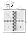
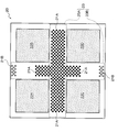
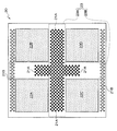
半導体回路がそれぞれ形成された矩形状の4つの第1~第4の半導体回路形成領域であって、直交する2辺を所定間隙を持って互いに対向させて配設される第1~第4の半導体回路形成領域と、
互いの前記第1~第4の半導体回路形成領域間により形成される間隙からなり、且つ直交する2つの第1~第2の領域で構成される十字状の電極配置領域と、
前記十字状の電極配置領域のうち、前記第1の領域内の少なくとも一部に配設され、前記半導体回路に接続され、前記半導体回路に電力又は信号を供給する第1の電極群と、
前記十字状の電極配置領域のうち、前記第2の領域内の少なくとも一部に配設され、前記半導体回路に接続され、前記半導体回路に電力又は信号を供給する第2の電極群と、
を備える半導体チップである。 The above problem is solved by the following means. That is,
The invention according to claim 1
Four first to fourth semiconductor circuit formation regions each having a rectangular shape in which semiconductor circuits are formed, and the first to fourth regions arranged with two orthogonal sides facing each other with a predetermined gap. A semiconductor circuit formation region;
A cross-shaped electrode arrangement region composed of two first to second regions that are orthogonal to each other and are formed by a gap formed between the first to fourth semiconductor circuit formation regions;
A first electrode group disposed in at least a part of the first region in the cross-shaped electrode arrangement region, connected to the semiconductor circuit, and supplying power or a signal to the semiconductor circuit;
A second electrode group disposed in at least part of the second region in the cross-shaped electrode arrangement region, connected to the semiconductor circuit, and supplying power or a signal to the semiconductor circuit;
It is a semiconductor chip provided with.
前記第1の電極群が信号入出力用の電極を含んで構成される電極群であると共に、前記第2の電極群が電力供給用の電極及び接地用の電極を含んで構成される電極群である請求項1に記載の半導体チップである。 The invention according to claim 2
The first electrode group is an electrode group including a signal input / output electrode, and the second electrode group is an electrode group including a power supply electrode and a ground electrode. The semiconductor chip according to claim 1.
前記半導体回路が記憶回路であると共に、前記半導体チップが記憶装置チップである請求項1又は2に記載の半導体チップである。 The invention according to claim 3
The semiconductor chip according to claim 1, wherein the semiconductor circuit is a memory circuit, and the semiconductor chip is a memory device chip.
配線チップと、
前記配線チップの主面上に、電極群を対向させて実装された第1の半導体チップと、
前記第1の半導体チップとは異なる第2の半導体チップであって、前記配線チップの主面上に、電極群を対向させて実装された第2の半導体チップと、
を備え、
前記第2の半導体チップが、請求項1~3のいずれか1項に記載の半導体チップである半導体装置である。 The invention according to claim 4
A wiring chip;
A first semiconductor chip mounted on the main surface of the wiring chip with the electrode groups facing each other;
A second semiconductor chip different from the first semiconductor chip, the second semiconductor chip mounted on the main surface of the wiring chip with the electrode groups facing each other;
With
The semiconductor device according to any one of claims 1 to 3, wherein the second semiconductor chip is a semiconductor chip.
第1の半導体チップと、
前記第1の半導体チップとは異なる第2の半導体チップであって、前記第1の半導体チップの主面上に、電極群を対向させて実装された第2の半導体チップと、
を備え、
前記第2の半導体チップが、請求項1~3のいずれか1項に記載の半導体チップである半導体装置である。 The invention according to claim 5
A first semiconductor chip;
A second semiconductor chip different from the first semiconductor chip, wherein the second semiconductor chip is mounted on the main surface of the first semiconductor chip with the electrode groups facing each other;
With
The semiconductor device according to any one of claims 1 to 3, wherein the second semiconductor chip is a semiconductor chip.
なお、ここで、上述した2つの記憶装置チップ20として256Mビットのマルチ・メディア・メモリとASIC30のバンド幅について説明する。前述したように、このバンド幅は、半導体装置の動作周波数と半導体装置の入出力データ数(入出力ビット数)の積として規定される。
例えば、本実施形態での半導体装置の動作周波数を33MHz、半導体装置の入出力データ数を256×2=512個とした場合、そのバンド幅は2.1GB/sとなる。 The wiring pitch of the
Here, the bandwidth of the 256 Mbit multimedia memory and the
For example, when the operating frequency of the semiconductor device in this embodiment is 33 MHz and the number of input / output data of the semiconductor device is 256 × 2 = 512, the bandwidth is 2.1 GB / s.
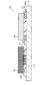
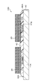
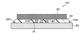
11A,11B 接続パッド
20 記憶装置チップ
21A 信号入出力用接続バンプ
21B 電力・接地用接続バンプ
22A、22B,22C、22D メモリバンク
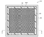
23 接続バンプ配置領域
23A、23B 領域
31 接続バンプ
40 半田
42 アンダーフィル樹脂
42A ダム部材
100 半導体装置
101 半導体装置 10
Claims (5)
- 半導体回路がそれぞれ形成された矩形状の4つの第1~第4の半導体回路形成領域であって、直交する2辺を所定間隙を持って互いに対向させて配設される第1~第4の半導体回路形成領域と、
互いの前記第1~第4の半導体回路形成領域間により形成される間隙からなり、且つ直交する2つの第1~第2の領域で構成される十字状の電極配置領域と、
前記十字状の電極配置領域のうち、前記第1の領域内の少なくとも一部に配設され、前記半導体回路に接続され、前記半導体回路に電力又は信号を供給する第1の電極群と、
前記十字状の電極配置領域のうち、前記第2の領域内の少なくとも一部に配設され、前記半導体回路に接続され、前記半導体回路に電力又は信号を供給する第2の電極群と、
を備える半導体チップ。 Four first to fourth semiconductor circuit formation regions each having a rectangular shape in which semiconductor circuits are formed, and the first to fourth regions arranged with two orthogonal sides facing each other with a predetermined gap. A semiconductor circuit formation region;
A cross-shaped electrode arrangement region composed of two first to second regions that are orthogonal to each other and are formed by a gap formed between the first to fourth semiconductor circuit formation regions;
A first electrode group disposed in at least a part of the first region in the cross-shaped electrode arrangement region, connected to the semiconductor circuit, and supplying power or a signal to the semiconductor circuit;
A second electrode group disposed in at least part of the second region in the cross-shaped electrode arrangement region, connected to the semiconductor circuit, and supplying power or a signal to the semiconductor circuit;
A semiconductor chip comprising: - 前記第1の電極群が信号入出力用の電極を含んで構成される電極群であると共に、前記第2の電極群が電力供給用の電極及び接地用の電極を含んで構成される電極群である請求項1に記載の半導体チップ。 The first electrode group is an electrode group including a signal input / output electrode, and the second electrode group is an electrode group including a power supply electrode and a ground electrode. The semiconductor chip according to claim 1.
- 前記半導体回路が記憶回路であると共に、前記半導体チップが記憶装置チップである請求項1又は2に記載の半導体チップ。 3. The semiconductor chip according to claim 1, wherein the semiconductor circuit is a memory circuit and the semiconductor chip is a memory device chip.
- 配線チップと、
前記配線チップの主面上に、電極群を対向させて実装された第1の半導体チップと、
前記第1の半導体チップとは異なる第2の半導体チップであって、前記配線チップの主面上に、電極群を対向させて実装された第2の半導体チップと、
を備え、
前記第2の半導体チップが、請求項1~3のいずれか1項に記載の半導体チップである半導体装置。 A wiring chip;
A first semiconductor chip mounted on the main surface of the wiring chip with the electrode groups facing each other;
A second semiconductor chip different from the first semiconductor chip, the second semiconductor chip mounted on the main surface of the wiring chip with the electrode groups facing each other;
With
The semiconductor device according to any one of claims 1 to 3, wherein the second semiconductor chip is a semiconductor chip. - 第1の半導体チップと、
前記第1の半導体チップとは異なる第2の半導体チップであって、前記第1の半導体チップの主面上に、電極群を対向させて実装された第2の半導体チップと、
を備え、
前記第2の半導体チップが、請求項1~3のいずれか1項に記載の半導体チップである半導体装置。 A first semiconductor chip;
A second semiconductor chip different from the first semiconductor chip, wherein the second semiconductor chip is mounted on the main surface of the first semiconductor chip with the electrode groups facing each other;
With
The semiconductor device according to any one of claims 1 to 3, wherein the second semiconductor chip is a semiconductor chip.
Priority Applications (3)
| Application Number | Priority Date | Filing Date | Title |
|---|---|---|---|
| CN2009801057659A CN101952956A (en) | 2008-02-19 | 2009-02-16 | Semiconductor chip and semiconductor device |
| EP09712660A EP2249381A4 (en) | 2008-02-19 | 2009-02-16 | Semiconductor chip and semiconductor device |
| US12/918,401 US20100327457A1 (en) | 2008-02-19 | 2009-02-16 | Semiconductor chip and semiconductor device |
Applications Claiming Priority (2)
| Application Number | Priority Date | Filing Date | Title |
|---|---|---|---|
| JP2008-037452 | 2008-02-19 | ||
| JP2008037452A JP2009200101A (en) | 2008-02-19 | 2008-02-19 | Semiconductor chip and semiconductor device |
Publications (1)
| Publication Number | Publication Date |
|---|---|
| WO2009104536A1 true WO2009104536A1 (en) | 2009-08-27 |
Family
ID=40985417
Family Applications (1)
| Application Number | Title | Priority Date | Filing Date |
|---|---|---|---|
| PCT/JP2009/052493 WO2009104536A1 (en) | 2008-02-19 | 2009-02-16 | Semiconductor chip and semiconductor device |
Country Status (7)
| Country | Link |
|---|---|
| US (1) | US20100327457A1 (en) |
| EP (1) | EP2249381A4 (en) |
| JP (1) | JP2009200101A (en) |
| KR (1) | KR20100123860A (en) |
| CN (1) | CN101952956A (en) |
| TW (1) | TW201001670A (en) |
| WO (1) | WO2009104536A1 (en) |
Families Citing this family (37)
| Publication number | Priority date | Publication date | Assignee | Title |
|---|---|---|---|---|
| JP2009295740A (en) * | 2008-06-04 | 2009-12-17 | Elpida Memory Inc | Memory chip and semiconductor device |
| JP5342422B2 (en) * | 2009-12-10 | 2013-11-13 | ルネサスエレクトロニクス株式会社 | Semiconductor device and manufacturing method thereof |
| US8796863B2 (en) | 2010-02-09 | 2014-08-05 | Samsung Electronics Co., Ltd. | Semiconductor memory devices and semiconductor packages |
| US8901747B2 (en) | 2010-07-29 | 2014-12-02 | Mosys, Inc. | Semiconductor chip layout |
| KR20120056018A (en) * | 2010-11-24 | 2012-06-01 | 삼성전자주식회사 | Semiconductor device with cross-shaped bumps and test pads arrangement |
| KR101262638B1 (en) | 2010-12-06 | 2013-05-08 | 기아자동차주식회사 | A solenoid valve for liquid propane injection system |
| JP5579108B2 (en) | 2011-03-16 | 2014-08-27 | 株式会社東芝 | Semiconductor device |
| US8823165B2 (en) | 2011-07-12 | 2014-09-02 | Invensas Corporation | Memory module in a package |
| US8513817B2 (en) | 2011-07-12 | 2013-08-20 | Invensas Corporation | Memory module in a package |
| US8502390B2 (en) | 2011-07-12 | 2013-08-06 | Tessera, Inc. | De-skewed multi-die packages |
| JP5947904B2 (en) | 2011-10-03 | 2016-07-06 | インヴェンサス・コーポレイション | Stub minimization for multi-die wirebond assemblies with orthogonal windows |
| US8441111B2 (en) | 2011-10-03 | 2013-05-14 | Invensas Corporation | Stub minimization for multi-die wirebond assemblies with parallel windows |
| KR101894823B1 (en) | 2011-10-03 | 2018-09-04 | 인벤사스 코포레이션 | Stub minimization for multi-die wirebond assemblies with parallel windows |
| US8436457B2 (en) | 2011-10-03 | 2013-05-07 | Invensas Corporation | Stub minimization for multi-die wirebond assemblies with parallel windows |
| US8659140B2 (en) | 2011-10-03 | 2014-02-25 | Invensas Corporation | Stub minimization using duplicate sets of signal terminals in assemblies without wirebonds to package substrate |
| US8513813B2 (en) | 2011-10-03 | 2013-08-20 | Invensas Corporation | Stub minimization using duplicate sets of terminals for wirebond assemblies without windows |
| US8525327B2 (en) | 2011-10-03 | 2013-09-03 | Invensas Corporation | Stub minimization for assemblies without wirebonds to package substrate |
| US8659143B2 (en) | 2011-10-03 | 2014-02-25 | Invensas Corporation | Stub minimization for wirebond assemblies without windows |
| WO2013052347A1 (en) * | 2011-10-03 | 2013-04-11 | Invensas Corporation | Memory module in a package and its pin configuration |
| KR20140069343A (en) | 2011-10-03 | 2014-06-09 | 인벤사스 코포레이션 | Stub minimization with terminal grids offset from center of package |
| US8759163B2 (en) * | 2012-04-30 | 2014-06-24 | Taiwan Semiconductor Manufacturing Co., Ltd. | Layout of a MOS array edge with density gradient smoothing |
| US9006908B2 (en) | 2012-08-01 | 2015-04-14 | Marvell Israel (M.I.S.L) Ltd. | Integrated circuit interposer and method of manufacturing the same |
| US8848391B2 (en) | 2012-08-27 | 2014-09-30 | Invensas Corporation | Co-support component and microelectronic assembly |
| US9368477B2 (en) | 2012-08-27 | 2016-06-14 | Invensas Corporation | Co-support circuit panel and microelectronic packages |
| US8848392B2 (en) | 2012-08-27 | 2014-09-30 | Invensas Corporation | Co-support module and microelectronic assembly |
| US8787034B2 (en) | 2012-08-27 | 2014-07-22 | Invensas Corporation | Co-support system and microelectronic assembly |
| US20140159238A1 (en) * | 2012-12-07 | 2014-06-12 | Qualcomm Incorporated | Package having thermal compression flip chip (tcfc) and chip with reflow bonding on lead |
| KR101324431B1 (en) * | 2013-05-14 | 2013-10-31 | 주식회사 한국인삼공사 | Composition effective for removing hangover |
| US9070423B2 (en) | 2013-06-11 | 2015-06-30 | Invensas Corporation | Single package dual channel memory with co-support |
| US9123555B2 (en) | 2013-10-25 | 2015-09-01 | Invensas Corporation | Co-support for XFD packaging |
| US9305131B2 (en) * | 2013-12-03 | 2016-04-05 | Mediatek Inc. | Method for flip chip packaging co-design |
| US9281296B2 (en) | 2014-07-31 | 2016-03-08 | Invensas Corporation | Die stacking techniques in BGA memory package for small footprint CPU and memory motherboard design |
| US9691437B2 (en) | 2014-09-25 | 2017-06-27 | Invensas Corporation | Compact microelectronic assembly having reduced spacing between controller and memory packages |
| US9659863B2 (en) | 2014-12-01 | 2017-05-23 | Taiwan Semiconductor Manufacturing Company, Ltd. | Semiconductor devices, multi-die packages, and methods of manufacture thereof |
| US9543192B2 (en) * | 2015-05-18 | 2017-01-10 | Globalfoundries Singapore Pte. Ltd. | Stitched devices |
| US9484080B1 (en) | 2015-11-09 | 2016-11-01 | Invensas Corporation | High-bandwidth memory application with controlled impedance loading |
| US9679613B1 (en) | 2016-05-06 | 2017-06-13 | Invensas Corporation | TFD I/O partition for high-speed, high-density applications |
Citations (9)
| Publication number | Priority date | Publication date | Assignee | Title |
|---|---|---|---|---|
| JPH07263449A (en) | 1994-03-18 | 1995-10-13 | Hitachi Ltd | Semiconductor device and its manufacture |
| JP2000188381A (en) | 1998-12-22 | 2000-07-04 | Toshiba Corp | Semiconductor storage device |
| JP2000315776A (en) | 1999-05-06 | 2000-11-14 | Hitachi Ltd | Semiconductor device |
| JP2002026037A (en) | 2000-07-05 | 2002-01-25 | Shinko Electric Ind Co Ltd | Wiring board and semiconductor device |
| JP2003258154A (en) | 2002-03-05 | 2003-09-12 | Fujitsu Ltd | Package structure of semiconductor device |
| JP2004063753A (en) * | 2002-07-29 | 2004-02-26 | Nec Kansai Ltd | Semiconductor chip for chip on chip connection and connecting method therefor |
| JP2004265940A (en) * | 2003-02-19 | 2004-09-24 | Sony Corp | Semiconductor device |
| JP2006147629A (en) | 2004-11-16 | 2006-06-08 | Matsushita Electric Works Ltd | Semiconductor device and its evaluation method |
| JP2007529930A (en) | 2004-03-19 | 2007-10-25 | フォルシュングスフェアブント ベルリン エー ファウ | Microwave antenna for semiconductor modules manufactured using flip-chip technology |
Family Cites Families (14)
| Publication number | Priority date | Publication date | Assignee | Title |
|---|---|---|---|---|
| JPH0562978A (en) * | 1991-08-30 | 1993-03-12 | Fujitsu Ltd | Flip chip |
| JP2006157047A (en) * | 1995-03-30 | 2006-06-15 | Renesas Technology Corp | Semiconductor package |
| JP3494502B2 (en) * | 1995-05-12 | 2004-02-09 | 株式会社ルネサステクノロジ | Semiconductor memory device and pad arrangement method thereof |
| US20040061220A1 (en) * | 1996-03-22 | 2004-04-01 | Chuichi Miyazaki | Semiconductor device and manufacturing method thereof |
| US5719449A (en) * | 1996-09-30 | 1998-02-17 | Lucent Technologies Inc. | Flip-chip integrated circuit with improved testability |
| WO1998035293A1 (en) * | 1997-02-07 | 1998-08-13 | T.I.F. Co., Ltd. | Memory system |
| JPH1131716A (en) * | 1997-07-11 | 1999-02-02 | Hitachi Ltd | Manufacture of semiconductor device and semiconductor chip |
| JP3259763B2 (en) * | 1997-11-14 | 2002-02-25 | 日本電気株式会社 | Semiconductor LSI |
| JP4776861B2 (en) * | 2002-09-26 | 2011-09-21 | ルネサスエレクトロニクス株式会社 | Semiconductor device |
| JP3722224B2 (en) * | 2003-12-24 | 2005-11-30 | セイコーエプソン株式会社 | Semiconductor chip, semiconductor device, and method of manufacturing semiconductor device |
| US7015592B2 (en) * | 2004-03-19 | 2006-03-21 | Intel Corporation | Marking on underfill |
| DE102004042073A1 (en) * | 2004-08-31 | 2006-03-09 | Infineon Technologies Ag | Circuit arrangement for data storage has memory device and controller on first and second circuit boards forming separate parts of circuit arrangement, connection device for providing data exchange between memory device and controller |
| US7684781B2 (en) * | 2005-11-25 | 2010-03-23 | Semiconductor Energy Laboratory Co., Ltd | Semiconductor device |
| JP2008066371A (en) * | 2006-09-05 | 2008-03-21 | Matsushita Electric Ind Co Ltd | Power supply wiring structure in semiconductor integrated circuit |
-
2008
- 2008-02-19 JP JP2008037452A patent/JP2009200101A/en active Pending
-
2009
- 2009-02-16 US US12/918,401 patent/US20100327457A1/en not_active Abandoned
- 2009-02-16 CN CN2009801057659A patent/CN101952956A/en active Pending
- 2009-02-16 KR KR1020107019920A patent/KR20100123860A/en not_active Application Discontinuation
- 2009-02-16 EP EP09712660A patent/EP2249381A4/en not_active Withdrawn
- 2009-02-16 WO PCT/JP2009/052493 patent/WO2009104536A1/en active Application Filing
- 2009-02-16 TW TW098104879A patent/TW201001670A/en unknown
Patent Citations (9)
| Publication number | Priority date | Publication date | Assignee | Title |
|---|---|---|---|---|
| JPH07263449A (en) | 1994-03-18 | 1995-10-13 | Hitachi Ltd | Semiconductor device and its manufacture |
| JP2000188381A (en) | 1998-12-22 | 2000-07-04 | Toshiba Corp | Semiconductor storage device |
| JP2000315776A (en) | 1999-05-06 | 2000-11-14 | Hitachi Ltd | Semiconductor device |
| JP2002026037A (en) | 2000-07-05 | 2002-01-25 | Shinko Electric Ind Co Ltd | Wiring board and semiconductor device |
| JP2003258154A (en) | 2002-03-05 | 2003-09-12 | Fujitsu Ltd | Package structure of semiconductor device |
| JP2004063753A (en) * | 2002-07-29 | 2004-02-26 | Nec Kansai Ltd | Semiconductor chip for chip on chip connection and connecting method therefor |
| JP2004265940A (en) * | 2003-02-19 | 2004-09-24 | Sony Corp | Semiconductor device |
| JP2007529930A (en) | 2004-03-19 | 2007-10-25 | フォルシュングスフェアブント ベルリン エー ファウ | Microwave antenna for semiconductor modules manufactured using flip-chip technology |
| JP2006147629A (en) | 2004-11-16 | 2006-06-08 | Matsushita Electric Works Ltd | Semiconductor device and its evaluation method |
Non-Patent Citations (1)
| Title |
|---|
| See also references of EP2249381A4 |
Also Published As
| Publication number | Publication date |
|---|---|
| KR20100123860A (en) | 2010-11-25 |
| EP2249381A4 (en) | 2012-11-21 |
| US20100327457A1 (en) | 2010-12-30 |
| EP2249381A1 (en) | 2010-11-10 |
| CN101952956A (en) | 2011-01-19 |
| JP2009200101A (en) | 2009-09-03 |
| TW201001670A (en) | 2010-01-01 |
Similar Documents
| Publication | Publication Date | Title |
|---|---|---|
| WO2009104536A1 (en) | Semiconductor chip and semiconductor device | |
| US11227639B2 (en) | Stacked DRAM device and method of manufacture | |
| US10037971B2 (en) | Semiconductor device having plural memory chip | |
| US8319351B2 (en) | Planar multi semiconductor chip package | |
| US8680652B2 (en) | Stack package | |
| JP3774468B2 (en) | Semiconductor device | |
| US9368477B2 (en) | Co-support circuit panel and microelectronic packages | |
| TWI761632B (en) | Semiconductor packages including bridge die spaced apart from semiconductor die | |
| JP3895756B1 (en) | Semiconductor device | |
| JP2015109408A (en) | Composite chip, semiconductor device, and manufacturing method of semiconductor device | |
| KR102426664B1 (en) | Integrated circuit having bump pads and semiconductor package including the same | |
| KR20220036534A (en) | Semiconductor chip including penetrating electrode, and semiconductor package including the same | |
| US8304879B2 (en) | Spiral staircase shaped stacked semiconductor package and method for manufacturing the same | |
| JP3813768B2 (en) | Semiconductor device and semiconductor module | |
| JP4658529B2 (en) | Structure of integrated circuit module | |
| CN114121873A (en) | Apparatus and system having ball grid array and related microelectronic device and device package | |
| JP6689420B2 (en) | Semiconductor device and method of manufacturing semiconductor device | |
| US20230130453A1 (en) | Semiconductor package, and memory module including the same | |
| JP3904587B1 (en) | Semiconductor device and manufacturing method thereof | |
| JP2007157182A (en) | Semiconductor apparatus | |
| CN115004355A (en) | Memory chip stack package and electronic device | |
| WO2014132835A1 (en) | Semiconductor device | |
| JPH03203259A (en) | Semiconductor module |
Legal Events
| Date | Code | Title | Description |
|---|---|---|---|
| WWE | Wipo information: entry into national phase |
Ref document number: 200980105765.9 Country of ref document: CN |
|
| 121 | Ep: the epo has been informed by wipo that ep was designated in this application |
Ref document number: 09712660 Country of ref document: EP Kind code of ref document: A1 |
|
| WWE | Wipo information: entry into national phase |
Ref document number: 12918401 Country of ref document: US |
|
| NENP | Non-entry into the national phase |
Ref country code: DE |
|
| ENP | Entry into the national phase |
Ref document number: 20107019920 Country of ref document: KR Kind code of ref document: A |
|
| WWE | Wipo information: entry into national phase |
Ref document number: 2009712660 Country of ref document: EP |