JP5342422B2 - Semiconductor device and manufacturing method thereof - Google Patents
Semiconductor device and manufacturing method thereof Download PDFInfo
- Publication number
- JP5342422B2 JP5342422B2 JP2009280469A JP2009280469A JP5342422B2 JP 5342422 B2 JP5342422 B2 JP 5342422B2 JP 2009280469 A JP2009280469 A JP 2009280469A JP 2009280469 A JP2009280469 A JP 2009280469A JP 5342422 B2 JP5342422 B2 JP 5342422B2
- Authority
- JP
- Japan
- Prior art keywords
- land
- wiring board
- semiconductor device
- contact pin
- lands
- Prior art date
- Legal status (The legal status is an assumption and is not a legal conclusion. Google has not performed a legal analysis and makes no representation as to the accuracy of the status listed.)
- Active
Links
Images


Classifications
-
- H—ELECTRICITY
- H01—ELECTRIC ELEMENTS
- H01L—SEMICONDUCTOR DEVICES NOT COVERED BY CLASS H10
- H01L23/00—Details of semiconductor or other solid state devices
- H01L23/48—Arrangements for conducting electric current to or from the solid state body in operation, e.g. leads, terminal arrangements ; Selection of materials therefor
- H01L23/488—Arrangements for conducting electric current to or from the solid state body in operation, e.g. leads, terminal arrangements ; Selection of materials therefor consisting of soldered or bonded constructions
- H01L23/498—Leads, i.e. metallisations or lead-frames on insulating substrates, e.g. chip carriers
- H01L23/49838—Geometry or layout
-
- H—ELECTRICITY
- H01—ELECTRIC ELEMENTS
- H01L—SEMICONDUCTOR DEVICES NOT COVERED BY CLASS H10
- H01L22/00—Testing or measuring during manufacture or treatment; Reliability measurements, i.e. testing of parts without further processing to modify the parts as such; Structural arrangements therefor
- H01L22/30—Structural arrangements specially adapted for testing or measuring during manufacture or treatment, or specially adapted for reliability measurements
- H01L22/32—Additional lead-in metallisation on a device or substrate, e.g. additional pads or pad portions, lines in the scribe line, sacrificed conductors
-
- H—ELECTRICITY
- H01—ELECTRIC ELEMENTS
- H01L—SEMICONDUCTOR DEVICES NOT COVERED BY CLASS H10
- H01L25/00—Assemblies consisting of a plurality of individual semiconductor or other solid state devices ; Multistep manufacturing processes thereof
- H01L25/03—Assemblies consisting of a plurality of individual semiconductor or other solid state devices ; Multistep manufacturing processes thereof all the devices being of a type provided for in the same subgroup of groups H01L27/00 - H01L33/00, or in a single subclass of H10K, H10N, e.g. assemblies of rectifier diodes
- H01L25/10—Assemblies consisting of a plurality of individual semiconductor or other solid state devices ; Multistep manufacturing processes thereof all the devices being of a type provided for in the same subgroup of groups H01L27/00 - H01L33/00, or in a single subclass of H10K, H10N, e.g. assemblies of rectifier diodes the devices having separate containers
- H01L25/105—Assemblies consisting of a plurality of individual semiconductor or other solid state devices ; Multistep manufacturing processes thereof all the devices being of a type provided for in the same subgroup of groups H01L27/00 - H01L33/00, or in a single subclass of H10K, H10N, e.g. assemblies of rectifier diodes the devices having separate containers the devices being of a type provided for in group H01L27/00
-
- H—ELECTRICITY
- H01—ELECTRIC ELEMENTS
- H01L—SEMICONDUCTOR DEVICES NOT COVERED BY CLASS H10
- H01L2224/00—Indexing scheme for arrangements for connecting or disconnecting semiconductor or solid-state bodies and methods related thereto as covered by H01L24/00
- H01L2224/01—Means for bonding being attached to, or being formed on, the surface to be connected, e.g. chip-to-package, die-attach, "first-level" interconnects; Manufacturing methods related thereto
- H01L2224/02—Bonding areas; Manufacturing methods related thereto
- H01L2224/04—Structure, shape, material or disposition of the bonding areas prior to the connecting process
- H01L2224/05—Structure, shape, material or disposition of the bonding areas prior to the connecting process of an individual bonding area
- H01L2224/0554—External layer
- H01L2224/0555—Shape
- H01L2224/05552—Shape in top view
- H01L2224/05554—Shape in top view being square
-
- H—ELECTRICITY
- H01—ELECTRIC ELEMENTS
- H01L—SEMICONDUCTOR DEVICES NOT COVERED BY CLASS H10
- H01L2224/00—Indexing scheme for arrangements for connecting or disconnecting semiconductor or solid-state bodies and methods related thereto as covered by H01L24/00
- H01L2224/01—Means for bonding being attached to, or being formed on, the surface to be connected, e.g. chip-to-package, die-attach, "first-level" interconnects; Manufacturing methods related thereto
- H01L2224/10—Bump connectors; Manufacturing methods related thereto
- H01L2224/15—Structure, shape, material or disposition of the bump connectors after the connecting process
- H01L2224/16—Structure, shape, material or disposition of the bump connectors after the connecting process of an individual bump connector
- H01L2224/161—Disposition
- H01L2224/16151—Disposition the bump connector connecting between a semiconductor or solid-state body and an item not being a semiconductor or solid-state body, e.g. chip-to-substrate, chip-to-passive
- H01L2224/16221—Disposition the bump connector connecting between a semiconductor or solid-state body and an item not being a semiconductor or solid-state body, e.g. chip-to-substrate, chip-to-passive the body and the item being stacked
- H01L2224/16225—Disposition the bump connector connecting between a semiconductor or solid-state body and an item not being a semiconductor or solid-state body, e.g. chip-to-substrate, chip-to-passive the body and the item being stacked the item being non-metallic, e.g. insulating substrate with or without metallisation
-
- H—ELECTRICITY
- H01—ELECTRIC ELEMENTS
- H01L—SEMICONDUCTOR DEVICES NOT COVERED BY CLASS H10
- H01L2224/00—Indexing scheme for arrangements for connecting or disconnecting semiconductor or solid-state bodies and methods related thereto as covered by H01L24/00
- H01L2224/01—Means for bonding being attached to, or being formed on, the surface to be connected, e.g. chip-to-package, die-attach, "first-level" interconnects; Manufacturing methods related thereto
- H01L2224/26—Layer connectors, e.g. plate connectors, solder or adhesive layers; Manufacturing methods related thereto
- H01L2224/31—Structure, shape, material or disposition of the layer connectors after the connecting process
- H01L2224/32—Structure, shape, material or disposition of the layer connectors after the connecting process of an individual layer connector
- H01L2224/321—Disposition
- H01L2224/32135—Disposition the layer connector connecting between different semiconductor or solid-state bodies, i.e. chip-to-chip
- H01L2224/32145—Disposition the layer connector connecting between different semiconductor or solid-state bodies, i.e. chip-to-chip the bodies being stacked
-
- H—ELECTRICITY
- H01—ELECTRIC ELEMENTS
- H01L—SEMICONDUCTOR DEVICES NOT COVERED BY CLASS H10
- H01L2224/00—Indexing scheme for arrangements for connecting or disconnecting semiconductor or solid-state bodies and methods related thereto as covered by H01L24/00
- H01L2224/01—Means for bonding being attached to, or being formed on, the surface to be connected, e.g. chip-to-package, die-attach, "first-level" interconnects; Manufacturing methods related thereto
- H01L2224/26—Layer connectors, e.g. plate connectors, solder or adhesive layers; Manufacturing methods related thereto
- H01L2224/31—Structure, shape, material or disposition of the layer connectors after the connecting process
- H01L2224/32—Structure, shape, material or disposition of the layer connectors after the connecting process of an individual layer connector
- H01L2224/321—Disposition
- H01L2224/32151—Disposition the layer connector connecting between a semiconductor or solid-state body and an item not being a semiconductor or solid-state body, e.g. chip-to-substrate, chip-to-passive
- H01L2224/32221—Disposition the layer connector connecting between a semiconductor or solid-state body and an item not being a semiconductor or solid-state body, e.g. chip-to-substrate, chip-to-passive the body and the item being stacked
- H01L2224/32225—Disposition the layer connector connecting between a semiconductor or solid-state body and an item not being a semiconductor or solid-state body, e.g. chip-to-substrate, chip-to-passive the body and the item being stacked the item being non-metallic, e.g. insulating substrate with or without metallisation
-
- H—ELECTRICITY
- H01—ELECTRIC ELEMENTS
- H01L—SEMICONDUCTOR DEVICES NOT COVERED BY CLASS H10
- H01L2224/00—Indexing scheme for arrangements for connecting or disconnecting semiconductor or solid-state bodies and methods related thereto as covered by H01L24/00
- H01L2224/01—Means for bonding being attached to, or being formed on, the surface to be connected, e.g. chip-to-package, die-attach, "first-level" interconnects; Manufacturing methods related thereto
- H01L2224/42—Wire connectors; Manufacturing methods related thereto
- H01L2224/44—Structure, shape, material or disposition of the wire connectors prior to the connecting process
- H01L2224/45—Structure, shape, material or disposition of the wire connectors prior to the connecting process of an individual wire connector
- H01L2224/45001—Core members of the connector
- H01L2224/45099—Material
- H01L2224/451—Material with a principal constituent of the material being a metal or a metalloid, e.g. boron (B), silicon (Si), germanium (Ge), arsenic (As), antimony (Sb), tellurium (Te) and polonium (Po), and alloys thereof
- H01L2224/45138—Material with a principal constituent of the material being a metal or a metalloid, e.g. boron (B), silicon (Si), germanium (Ge), arsenic (As), antimony (Sb), tellurium (Te) and polonium (Po), and alloys thereof the principal constituent melting at a temperature of greater than or equal to 950°C and less than 1550°C
- H01L2224/45144—Gold (Au) as principal constituent
-
- H—ELECTRICITY
- H01—ELECTRIC ELEMENTS
- H01L—SEMICONDUCTOR DEVICES NOT COVERED BY CLASS H10
- H01L2224/00—Indexing scheme for arrangements for connecting or disconnecting semiconductor or solid-state bodies and methods related thereto as covered by H01L24/00
- H01L2224/01—Means for bonding being attached to, or being formed on, the surface to be connected, e.g. chip-to-package, die-attach, "first-level" interconnects; Manufacturing methods related thereto
- H01L2224/42—Wire connectors; Manufacturing methods related thereto
- H01L2224/47—Structure, shape, material or disposition of the wire connectors after the connecting process
- H01L2224/48—Structure, shape, material or disposition of the wire connectors after the connecting process of an individual wire connector
- H01L2224/481—Disposition
- H01L2224/48151—Connecting between a semiconductor or solid-state body and an item not being a semiconductor or solid-state body, e.g. chip-to-substrate, chip-to-passive
- H01L2224/48221—Connecting between a semiconductor or solid-state body and an item not being a semiconductor or solid-state body, e.g. chip-to-substrate, chip-to-passive the body and the item being stacked
- H01L2224/48225—Connecting between a semiconductor or solid-state body and an item not being a semiconductor or solid-state body, e.g. chip-to-substrate, chip-to-passive the body and the item being stacked the item being non-metallic, e.g. insulating substrate with or without metallisation
- H01L2224/48227—Connecting between a semiconductor or solid-state body and an item not being a semiconductor or solid-state body, e.g. chip-to-substrate, chip-to-passive the body and the item being stacked the item being non-metallic, e.g. insulating substrate with or without metallisation connecting the wire to a bond pad of the item
- H01L2224/48228—Connecting between a semiconductor or solid-state body and an item not being a semiconductor or solid-state body, e.g. chip-to-substrate, chip-to-passive the body and the item being stacked the item being non-metallic, e.g. insulating substrate with or without metallisation connecting the wire to a bond pad of the item the bond pad being disposed in a recess of the surface of the item
-
- H—ELECTRICITY
- H01—ELECTRIC ELEMENTS
- H01L—SEMICONDUCTOR DEVICES NOT COVERED BY CLASS H10
- H01L2224/00—Indexing scheme for arrangements for connecting or disconnecting semiconductor or solid-state bodies and methods related thereto as covered by H01L24/00
- H01L2224/01—Means for bonding being attached to, or being formed on, the surface to be connected, e.g. chip-to-package, die-attach, "first-level" interconnects; Manufacturing methods related thereto
- H01L2224/42—Wire connectors; Manufacturing methods related thereto
- H01L2224/47—Structure, shape, material or disposition of the wire connectors after the connecting process
- H01L2224/48—Structure, shape, material or disposition of the wire connectors after the connecting process of an individual wire connector
- H01L2224/481—Disposition
- H01L2224/48151—Connecting between a semiconductor or solid-state body and an item not being a semiconductor or solid-state body, e.g. chip-to-substrate, chip-to-passive
- H01L2224/48221—Connecting between a semiconductor or solid-state body and an item not being a semiconductor or solid-state body, e.g. chip-to-substrate, chip-to-passive the body and the item being stacked
- H01L2224/48225—Connecting between a semiconductor or solid-state body and an item not being a semiconductor or solid-state body, e.g. chip-to-substrate, chip-to-passive the body and the item being stacked the item being non-metallic, e.g. insulating substrate with or without metallisation
- H01L2224/48227—Connecting between a semiconductor or solid-state body and an item not being a semiconductor or solid-state body, e.g. chip-to-substrate, chip-to-passive the body and the item being stacked the item being non-metallic, e.g. insulating substrate with or without metallisation connecting the wire to a bond pad of the item
- H01L2224/48229—Connecting between a semiconductor or solid-state body and an item not being a semiconductor or solid-state body, e.g. chip-to-substrate, chip-to-passive the body and the item being stacked the item being non-metallic, e.g. insulating substrate with or without metallisation connecting the wire to a bond pad of the item the bond pad protruding from the surface of the item
-
- H—ELECTRICITY
- H01—ELECTRIC ELEMENTS
- H01L—SEMICONDUCTOR DEVICES NOT COVERED BY CLASS H10
- H01L2224/00—Indexing scheme for arrangements for connecting or disconnecting semiconductor or solid-state bodies and methods related thereto as covered by H01L24/00
- H01L2224/01—Means for bonding being attached to, or being formed on, the surface to be connected, e.g. chip-to-package, die-attach, "first-level" interconnects; Manufacturing methods related thereto
- H01L2224/42—Wire connectors; Manufacturing methods related thereto
- H01L2224/47—Structure, shape, material or disposition of the wire connectors after the connecting process
- H01L2224/49—Structure, shape, material or disposition of the wire connectors after the connecting process of a plurality of wire connectors
- H01L2224/491—Disposition
- H01L2224/4912—Layout
- H01L2224/49175—Parallel arrangements
-
- H—ELECTRICITY
- H01—ELECTRIC ELEMENTS
- H01L—SEMICONDUCTOR DEVICES NOT COVERED BY CLASS H10
- H01L2224/00—Indexing scheme for arrangements for connecting or disconnecting semiconductor or solid-state bodies and methods related thereto as covered by H01L24/00
- H01L2224/73—Means for bonding being of different types provided for in two or more of groups H01L2224/10, H01L2224/18, H01L2224/26, H01L2224/34, H01L2224/42, H01L2224/50, H01L2224/63, H01L2224/71
- H01L2224/732—Location after the connecting process
- H01L2224/73201—Location after the connecting process on the same surface
- H01L2224/73203—Bump and layer connectors
- H01L2224/73204—Bump and layer connectors the bump connector being embedded into the layer connector
-
- H—ELECTRICITY
- H01—ELECTRIC ELEMENTS
- H01L—SEMICONDUCTOR DEVICES NOT COVERED BY CLASS H10
- H01L2224/00—Indexing scheme for arrangements for connecting or disconnecting semiconductor or solid-state bodies and methods related thereto as covered by H01L24/00
- H01L2224/73—Means for bonding being of different types provided for in two or more of groups H01L2224/10, H01L2224/18, H01L2224/26, H01L2224/34, H01L2224/42, H01L2224/50, H01L2224/63, H01L2224/71
- H01L2224/732—Location after the connecting process
- H01L2224/73251—Location after the connecting process on different surfaces
- H01L2224/73253—Bump and layer connectors
-
- H—ELECTRICITY
- H01—ELECTRIC ELEMENTS
- H01L—SEMICONDUCTOR DEVICES NOT COVERED BY CLASS H10
- H01L2224/00—Indexing scheme for arrangements for connecting or disconnecting semiconductor or solid-state bodies and methods related thereto as covered by H01L24/00
- H01L2224/73—Means for bonding being of different types provided for in two or more of groups H01L2224/10, H01L2224/18, H01L2224/26, H01L2224/34, H01L2224/42, H01L2224/50, H01L2224/63, H01L2224/71
- H01L2224/732—Location after the connecting process
- H01L2224/73251—Location after the connecting process on different surfaces
- H01L2224/73265—Layer and wire connectors
-
- H—ELECTRICITY
- H01—ELECTRIC ELEMENTS
- H01L—SEMICONDUCTOR DEVICES NOT COVERED BY CLASS H10
- H01L2225/00—Details relating to assemblies covered by the group H01L25/00 but not provided for in its subgroups
- H01L2225/03—All the devices being of a type provided for in the same subgroup of groups H01L27/00 - H01L33/648 and H10K99/00
- H01L2225/04—All the devices being of a type provided for in the same subgroup of groups H01L27/00 - H01L33/648 and H10K99/00 the devices not having separate containers
- H01L2225/065—All the devices being of a type provided for in the same subgroup of groups H01L27/00 - H01L33/648 and H10K99/00 the devices not having separate containers the devices being of a type provided for in group H01L27/00
- H01L2225/06503—Stacked arrangements of devices
- H01L2225/06555—Geometry of the stack, e.g. form of the devices, geometry to facilitate stacking
- H01L2225/06562—Geometry of the stack, e.g. form of the devices, geometry to facilitate stacking at least one device in the stack being rotated or offset
-
- H—ELECTRICITY
- H01—ELECTRIC ELEMENTS
- H01L—SEMICONDUCTOR DEVICES NOT COVERED BY CLASS H10
- H01L2225/00—Details relating to assemblies covered by the group H01L25/00 but not provided for in its subgroups
- H01L2225/03—All the devices being of a type provided for in the same subgroup of groups H01L27/00 - H01L33/648 and H10K99/00
- H01L2225/10—All the devices being of a type provided for in the same subgroup of groups H01L27/00 - H01L33/648 and H10K99/00 the devices having separate containers
- H01L2225/1005—All the devices being of a type provided for in the same subgroup of groups H01L27/00 - H01L33/648 and H10K99/00 the devices having separate containers the devices being of a type provided for in group H01L27/00
- H01L2225/1011—All the devices being of a type provided for in the same subgroup of groups H01L27/00 - H01L33/648 and H10K99/00 the devices having separate containers the devices being of a type provided for in group H01L27/00 the containers being in a stacked arrangement
- H01L2225/1017—All the devices being of a type provided for in the same subgroup of groups H01L27/00 - H01L33/648 and H10K99/00 the devices having separate containers the devices being of a type provided for in group H01L27/00 the containers being in a stacked arrangement the lowermost container comprising a device support
- H01L2225/1023—All the devices being of a type provided for in the same subgroup of groups H01L27/00 - H01L33/648 and H10K99/00 the devices having separate containers the devices being of a type provided for in group H01L27/00 the containers being in a stacked arrangement the lowermost container comprising a device support the support being an insulating substrate
-
- H—ELECTRICITY
- H01—ELECTRIC ELEMENTS
- H01L—SEMICONDUCTOR DEVICES NOT COVERED BY CLASS H10
- H01L2225/00—Details relating to assemblies covered by the group H01L25/00 but not provided for in its subgroups
- H01L2225/03—All the devices being of a type provided for in the same subgroup of groups H01L27/00 - H01L33/648 and H10K99/00
- H01L2225/10—All the devices being of a type provided for in the same subgroup of groups H01L27/00 - H01L33/648 and H10K99/00 the devices having separate containers
- H01L2225/1005—All the devices being of a type provided for in the same subgroup of groups H01L27/00 - H01L33/648 and H10K99/00 the devices having separate containers the devices being of a type provided for in group H01L27/00
- H01L2225/1011—All the devices being of a type provided for in the same subgroup of groups H01L27/00 - H01L33/648 and H10K99/00 the devices having separate containers the devices being of a type provided for in group H01L27/00 the containers being in a stacked arrangement
- H01L2225/1047—Details of electrical connections between containers
- H01L2225/1058—Bump or bump-like electrical connections, e.g. balls, pillars, posts
-
- H—ELECTRICITY
- H01—ELECTRIC ELEMENTS
- H01L—SEMICONDUCTOR DEVICES NOT COVERED BY CLASS H10
- H01L23/00—Details of semiconductor or other solid state devices
- H01L23/28—Encapsulations, e.g. encapsulating layers, coatings, e.g. for protection
- H01L23/31—Encapsulations, e.g. encapsulating layers, coatings, e.g. for protection characterised by the arrangement or shape
- H01L23/3107—Encapsulations, e.g. encapsulating layers, coatings, e.g. for protection characterised by the arrangement or shape the device being completely enclosed
- H01L23/3121—Encapsulations, e.g. encapsulating layers, coatings, e.g. for protection characterised by the arrangement or shape the device being completely enclosed a substrate forming part of the encapsulation
-
- H—ELECTRICITY
- H01—ELECTRIC ELEMENTS
- H01L—SEMICONDUCTOR DEVICES NOT COVERED BY CLASS H10
- H01L23/00—Details of semiconductor or other solid state devices
- H01L23/48—Arrangements for conducting electric current to or from the solid state body in operation, e.g. leads, terminal arrangements ; Selection of materials therefor
- H01L23/488—Arrangements for conducting electric current to or from the solid state body in operation, e.g. leads, terminal arrangements ; Selection of materials therefor consisting of soldered or bonded constructions
- H01L23/498—Leads, i.e. metallisations or lead-frames on insulating substrates, e.g. chip carriers
- H01L23/49811—Additional leads joined to the metallisation on the insulating substrate, e.g. pins, bumps, wires, flat leads
- H01L23/49816—Spherical bumps on the substrate for external connection, e.g. ball grid arrays [BGA]
-
- H—ELECTRICITY
- H01—ELECTRIC ELEMENTS
- H01L—SEMICONDUCTOR DEVICES NOT COVERED BY CLASS H10
- H01L24/00—Arrangements for connecting or disconnecting semiconductor or solid-state bodies; Methods or apparatus related thereto
- H01L24/01—Means for bonding being attached to, or being formed on, the surface to be connected, e.g. chip-to-package, die-attach, "first-level" interconnects; Manufacturing methods related thereto
- H01L24/10—Bump connectors ; Manufacturing methods related thereto
- H01L24/15—Structure, shape, material or disposition of the bump connectors after the connecting process
- H01L24/16—Structure, shape, material or disposition of the bump connectors after the connecting process of an individual bump connector
-
- H—ELECTRICITY
- H01—ELECTRIC ELEMENTS
- H01L—SEMICONDUCTOR DEVICES NOT COVERED BY CLASS H10
- H01L24/00—Arrangements for connecting or disconnecting semiconductor or solid-state bodies; Methods or apparatus related thereto
- H01L24/01—Means for bonding being attached to, or being formed on, the surface to be connected, e.g. chip-to-package, die-attach, "first-level" interconnects; Manufacturing methods related thereto
- H01L24/26—Layer connectors, e.g. plate connectors, solder or adhesive layers; Manufacturing methods related thereto
- H01L24/28—Structure, shape, material or disposition of the layer connectors prior to the connecting process
- H01L24/29—Structure, shape, material or disposition of the layer connectors prior to the connecting process of an individual layer connector
-
- H—ELECTRICITY
- H01—ELECTRIC ELEMENTS
- H01L—SEMICONDUCTOR DEVICES NOT COVERED BY CLASS H10
- H01L24/00—Arrangements for connecting or disconnecting semiconductor or solid-state bodies; Methods or apparatus related thereto
- H01L24/01—Means for bonding being attached to, or being formed on, the surface to be connected, e.g. chip-to-package, die-attach, "first-level" interconnects; Manufacturing methods related thereto
- H01L24/26—Layer connectors, e.g. plate connectors, solder or adhesive layers; Manufacturing methods related thereto
- H01L24/31—Structure, shape, material or disposition of the layer connectors after the connecting process
- H01L24/32—Structure, shape, material or disposition of the layer connectors after the connecting process of an individual layer connector
-
- H—ELECTRICITY
- H01—ELECTRIC ELEMENTS
- H01L—SEMICONDUCTOR DEVICES NOT COVERED BY CLASS H10
- H01L24/00—Arrangements for connecting or disconnecting semiconductor or solid-state bodies; Methods or apparatus related thereto
- H01L24/01—Means for bonding being attached to, or being formed on, the surface to be connected, e.g. chip-to-package, die-attach, "first-level" interconnects; Manufacturing methods related thereto
- H01L24/42—Wire connectors; Manufacturing methods related thereto
- H01L24/44—Structure, shape, material or disposition of the wire connectors prior to the connecting process
- H01L24/45—Structure, shape, material or disposition of the wire connectors prior to the connecting process of an individual wire connector
-
- H—ELECTRICITY
- H01—ELECTRIC ELEMENTS
- H01L—SEMICONDUCTOR DEVICES NOT COVERED BY CLASS H10
- H01L24/00—Arrangements for connecting or disconnecting semiconductor or solid-state bodies; Methods or apparatus related thereto
- H01L24/01—Means for bonding being attached to, or being formed on, the surface to be connected, e.g. chip-to-package, die-attach, "first-level" interconnects; Manufacturing methods related thereto
- H01L24/42—Wire connectors; Manufacturing methods related thereto
- H01L24/47—Structure, shape, material or disposition of the wire connectors after the connecting process
- H01L24/48—Structure, shape, material or disposition of the wire connectors after the connecting process of an individual wire connector
-
- H—ELECTRICITY
- H01—ELECTRIC ELEMENTS
- H01L—SEMICONDUCTOR DEVICES NOT COVERED BY CLASS H10
- H01L24/00—Arrangements for connecting or disconnecting semiconductor or solid-state bodies; Methods or apparatus related thereto
- H01L24/01—Means for bonding being attached to, or being formed on, the surface to be connected, e.g. chip-to-package, die-attach, "first-level" interconnects; Manufacturing methods related thereto
- H01L24/42—Wire connectors; Manufacturing methods related thereto
- H01L24/47—Structure, shape, material or disposition of the wire connectors after the connecting process
- H01L24/49—Structure, shape, material or disposition of the wire connectors after the connecting process of a plurality of wire connectors
-
- H—ELECTRICITY
- H01—ELECTRIC ELEMENTS
- H01L—SEMICONDUCTOR DEVICES NOT COVERED BY CLASS H10
- H01L24/00—Arrangements for connecting or disconnecting semiconductor or solid-state bodies; Methods or apparatus related thereto
- H01L24/73—Means for bonding being of different types provided for in two or more of groups H01L24/10, H01L24/18, H01L24/26, H01L24/34, H01L24/42, H01L24/50, H01L24/63, H01L24/71
-
- H—ELECTRICITY
- H01—ELECTRIC ELEMENTS
- H01L—SEMICONDUCTOR DEVICES NOT COVERED BY CLASS H10
- H01L25/00—Assemblies consisting of a plurality of individual semiconductor or other solid state devices ; Multistep manufacturing processes thereof
- H01L25/03—Assemblies consisting of a plurality of individual semiconductor or other solid state devices ; Multistep manufacturing processes thereof all the devices being of a type provided for in the same subgroup of groups H01L27/00 - H01L33/00, or in a single subclass of H10K, H10N, e.g. assemblies of rectifier diodes
- H01L25/04—Assemblies consisting of a plurality of individual semiconductor or other solid state devices ; Multistep manufacturing processes thereof all the devices being of a type provided for in the same subgroup of groups H01L27/00 - H01L33/00, or in a single subclass of H10K, H10N, e.g. assemblies of rectifier diodes the devices not having separate containers
- H01L25/065—Assemblies consisting of a plurality of individual semiconductor or other solid state devices ; Multistep manufacturing processes thereof all the devices being of a type provided for in the same subgroup of groups H01L27/00 - H01L33/00, or in a single subclass of H10K, H10N, e.g. assemblies of rectifier diodes the devices not having separate containers the devices being of a type provided for in group H01L27/00
- H01L25/0657—Stacked arrangements of devices
-
- H—ELECTRICITY
- H01—ELECTRIC ELEMENTS
- H01L—SEMICONDUCTOR DEVICES NOT COVERED BY CLASS H10
- H01L2924/00—Indexing scheme for arrangements or methods for connecting or disconnecting semiconductor or solid-state bodies as covered by H01L24/00
- H01L2924/0001—Technical content checked by a classifier
- H01L2924/00014—Technical content checked by a classifier the subject-matter covered by the group, the symbol of which is combined with the symbol of this group, being disclosed without further technical details
-
- H—ELECTRICITY
- H01—ELECTRIC ELEMENTS
- H01L—SEMICONDUCTOR DEVICES NOT COVERED BY CLASS H10
- H01L2924/00—Indexing scheme for arrangements or methods for connecting or disconnecting semiconductor or solid-state bodies as covered by H01L24/00
- H01L2924/01—Chemical elements
- H01L2924/01013—Aluminum [Al]
-
- H—ELECTRICITY
- H01—ELECTRIC ELEMENTS
- H01L—SEMICONDUCTOR DEVICES NOT COVERED BY CLASS H10
- H01L2924/00—Indexing scheme for arrangements or methods for connecting or disconnecting semiconductor or solid-state bodies as covered by H01L24/00
- H01L2924/01—Chemical elements
- H01L2924/01014—Silicon [Si]
-
- H—ELECTRICITY
- H01—ELECTRIC ELEMENTS
- H01L—SEMICONDUCTOR DEVICES NOT COVERED BY CLASS H10
- H01L2924/00—Indexing scheme for arrangements or methods for connecting or disconnecting semiconductor or solid-state bodies as covered by H01L24/00
- H01L2924/01—Chemical elements
- H01L2924/01028—Nickel [Ni]
-
- H—ELECTRICITY
- H01—ELECTRIC ELEMENTS
- H01L—SEMICONDUCTOR DEVICES NOT COVERED BY CLASS H10
- H01L2924/00—Indexing scheme for arrangements or methods for connecting or disconnecting semiconductor or solid-state bodies as covered by H01L24/00
- H01L2924/01—Chemical elements
- H01L2924/0105—Tin [Sn]
-
- H—ELECTRICITY
- H01—ELECTRIC ELEMENTS
- H01L—SEMICONDUCTOR DEVICES NOT COVERED BY CLASS H10
- H01L2924/00—Indexing scheme for arrangements or methods for connecting or disconnecting semiconductor or solid-state bodies as covered by H01L24/00
- H01L2924/01—Chemical elements
- H01L2924/01078—Platinum [Pt]
-
- H—ELECTRICITY
- H01—ELECTRIC ELEMENTS
- H01L—SEMICONDUCTOR DEVICES NOT COVERED BY CLASS H10
- H01L2924/00—Indexing scheme for arrangements or methods for connecting or disconnecting semiconductor or solid-state bodies as covered by H01L24/00
- H01L2924/01—Chemical elements
- H01L2924/01079—Gold [Au]
-
- H—ELECTRICITY
- H01—ELECTRIC ELEMENTS
- H01L—SEMICONDUCTOR DEVICES NOT COVERED BY CLASS H10
- H01L2924/00—Indexing scheme for arrangements or methods for connecting or disconnecting semiconductor or solid-state bodies as covered by H01L24/00
- H01L2924/06—Polymers
- H01L2924/078—Adhesive characteristics other than chemical
-
- H—ELECTRICITY
- H01—ELECTRIC ELEMENTS
- H01L—SEMICONDUCTOR DEVICES NOT COVERED BY CLASS H10
- H01L2924/00—Indexing scheme for arrangements or methods for connecting or disconnecting semiconductor or solid-state bodies as covered by H01L24/00
- H01L2924/10—Details of semiconductor or other solid state devices to be connected
- H01L2924/1015—Shape
- H01L2924/1016—Shape being a cuboid
- H01L2924/10161—Shape being a cuboid with a rectangular active surface
-
- H—ELECTRICITY
- H01—ELECTRIC ELEMENTS
- H01L—SEMICONDUCTOR DEVICES NOT COVERED BY CLASS H10
- H01L2924/00—Indexing scheme for arrangements or methods for connecting or disconnecting semiconductor or solid-state bodies as covered by H01L24/00
- H01L2924/10—Details of semiconductor or other solid state devices to be connected
- H01L2924/1015—Shape
- H01L2924/1016—Shape being a cuboid
- H01L2924/10162—Shape being a cuboid with a square active surface
-
- H—ELECTRICITY
- H01—ELECTRIC ELEMENTS
- H01L—SEMICONDUCTOR DEVICES NOT COVERED BY CLASS H10
- H01L2924/00—Indexing scheme for arrangements or methods for connecting or disconnecting semiconductor or solid-state bodies as covered by H01L24/00
- H01L2924/10—Details of semiconductor or other solid state devices to be connected
- H01L2924/11—Device type
- H01L2924/14—Integrated circuits
-
- H—ELECTRICITY
- H01—ELECTRIC ELEMENTS
- H01L—SEMICONDUCTOR DEVICES NOT COVERED BY CLASS H10
- H01L2924/00—Indexing scheme for arrangements or methods for connecting or disconnecting semiconductor or solid-state bodies as covered by H01L24/00
- H01L2924/15—Details of package parts other than the semiconductor or other solid state devices to be connected
- H01L2924/151—Die mounting substrate
- H01L2924/1517—Multilayer substrate
- H01L2924/15192—Resurf arrangement of the internal vias
-
- H—ELECTRICITY
- H01—ELECTRIC ELEMENTS
- H01L—SEMICONDUCTOR DEVICES NOT COVERED BY CLASS H10
- H01L2924/00—Indexing scheme for arrangements or methods for connecting or disconnecting semiconductor or solid-state bodies as covered by H01L24/00
- H01L2924/15—Details of package parts other than the semiconductor or other solid state devices to be connected
- H01L2924/151—Die mounting substrate
- H01L2924/153—Connection portion
- H01L2924/1531—Connection portion the connection portion being formed only on the surface of the substrate opposite to the die mounting surface
- H01L2924/15311—Connection portion the connection portion being formed only on the surface of the substrate opposite to the die mounting surface being a ball array, e.g. BGA
-
- H—ELECTRICITY
- H01—ELECTRIC ELEMENTS
- H01L—SEMICONDUCTOR DEVICES NOT COVERED BY CLASS H10
- H01L2924/00—Indexing scheme for arrangements or methods for connecting or disconnecting semiconductor or solid-state bodies as covered by H01L24/00
- H01L2924/15—Details of package parts other than the semiconductor or other solid state devices to be connected
- H01L2924/151—Die mounting substrate
- H01L2924/153—Connection portion
- H01L2924/1532—Connection portion the connection portion being formed on the die mounting surface of the substrate
- H01L2924/1533—Connection portion the connection portion being formed on the die mounting surface of the substrate the connection portion being formed both on the die mounting surface of the substrate and outside the die mounting surface of the substrate
- H01L2924/15331—Connection portion the connection portion being formed on the die mounting surface of the substrate the connection portion being formed both on the die mounting surface of the substrate and outside the die mounting surface of the substrate being a ball array, e.g. BGA
-
- H—ELECTRICITY
- H01—ELECTRIC ELEMENTS
- H01L—SEMICONDUCTOR DEVICES NOT COVERED BY CLASS H10
- H01L2924/00—Indexing scheme for arrangements or methods for connecting or disconnecting semiconductor or solid-state bodies as covered by H01L24/00
- H01L2924/30—Technical effects
- H01L2924/301—Electrical effects
- H01L2924/3011—Impedance
-
- H—ELECTRICITY
- H01—ELECTRIC ELEMENTS
- H01L—SEMICONDUCTOR DEVICES NOT COVERED BY CLASS H10
- H01L2924/00—Indexing scheme for arrangements or methods for connecting or disconnecting semiconductor or solid-state bodies as covered by H01L24/00
- H01L2924/30—Technical effects
- H01L2924/35—Mechanical effects
- H01L2924/351—Thermal stress
- H01L2924/3511—Warping
Abstract
Description
本発明は、半導体装置およびその製造技術に関し、特に、半導体チップが搭載された配線基板の下面にテスト用ランドを設けた面実装型の半導体装置およびその製造に適用して有効な技術に関するものである。 The present invention relates to a semiconductor device and a manufacturing technique thereof, and more particularly to a surface mount type semiconductor device in which a test land is provided on a lower surface of a wiring board on which a semiconductor chip is mounted, and a technique effective when applied to the manufacturing thereof. is there.
SiP(システムインパッケージ)やBGA(ボールグリッドアレイ)のような面実装パッケージ形態を有する半導体装置は、パッケージ基板と呼ばれる配線基板の上面に搭載した1枚または複数枚の半導体チップ(以下、単にチップという)を樹脂で封止した構造を有している。 A semiconductor device having a surface mount package form such as SiP (system in package) or BGA (ball grid array) has one or more semiconductor chips (hereinafter simply referred to as chips) mounted on an upper surface of a wiring board called a package substrate. And) are sealed with resin.
上記配線基板の上面には複数の配線が形成されており、これらの配線の一端(ボンディングリード)とチップとは、金属ワイヤあるいはバンプ電極を介して電気的に接続される。一方、配線基板の下面には、配線基板内のビアホールを通じて上記配線に電気的に接続された複数のランドが設けられる。これらのランドは、半導体装置の外部端子を構成しており、半導体装置は、これらのランドに接続された半田バンプを介して各種電子機器のマザーボード(実装基板)に実装される。 A plurality of wirings are formed on the upper surface of the wiring board, and one end (bonding lead) of these wirings and the chip are electrically connected via metal wires or bump electrodes. On the other hand, a plurality of lands electrically connected to the wiring through via holes in the wiring board are provided on the lower surface of the wiring board. These lands constitute external terminals of the semiconductor device, and the semiconductor device is mounted on a mother board (mounting substrate) of various electronic devices via solder bumps connected to these lands.
また、配線基板の下面には、上記した外部端子としてのランドの他に、半導体製造メーカがチップの電気特性検査を行うためのテスト用ランドが設けられる。この電気特性検査は、上記半田バンプおよびテスト用ランドのそれぞれの表面にプローブ針と呼ばれる金属製のコンタクトピンを接触させ、チップに形成された集積回路の良否や、チップから配線基板のランドに至る配線経路の導通・非導通などを判別する試験である。 Further, on the lower surface of the wiring board, in addition to the lands as external terminals described above, a test land for a semiconductor manufacturer to inspect the electrical characteristics of the chip is provided. In this electrical characteristic inspection, metal contact pins called probe needles are brought into contact with the respective surfaces of the solder bumps and the test lands, and the quality of the integrated circuit formed on the chip, and the land from the chip to the land of the wiring board. This is a test for discriminating conduction / non-conduction of wiring paths.
例えば特許文献1(特開2006−93189号公報)には、配線基板の上面にマイコンチップとメモリチップとを2段に積み重ねて実装し、これらのチップをモールド樹脂で封止したSiP型の半導体装置において、配線基板の下面の周辺部に複数の電極(5c)を外部端子として配置し、これらの電極5cの内側にメモリチップの評価、信頼度試験および不良解析などを行う複数の電極(5d)を試験端子として配置する技術が開示されている。 For example, in Patent Document 1 (Japanese Patent Laid-Open No. 2006-93189), a SiP type semiconductor in which microcomputer chips and memory chips are stacked and mounted on the upper surface of a wiring board and these chips are sealed with a mold resin. In the apparatus, a plurality of electrodes (5c) are arranged as external terminals on the peripheral portion of the lower surface of the wiring board, and a plurality of electrodes (5d) for performing evaluation, reliability test, failure analysis, etc. of the memory chip inside these electrodes 5c. ) As a test terminal is disclosed.
上記SiPの外部端子を構成する電極5cには半田バンプが接続されるのに対し、試験端子を構成する電極5dには半田バンプが接続されず、平坦なLGA(Land Grid Array)構成となっている。また、互いに隣接する電極5dのピッチは、互いに隣接する電極5cのピッチと同じであるが、電極5dの直径は電極5cの直径よりも小さい。さらに、電極5dの表面は、電極5cに接続された半田バンプとの短絡ポテンシャルを低減させるために、ソルダレジストで被覆されている。メモリチップの試験時には、電極5dの表面を覆うソルダレジストを除去し、露出した電極5dにプローブ針を接触させる。 Solder bumps are connected to the electrodes 5c constituting the external terminals of the SiP, whereas solder bumps are not connected to the electrodes 5d constituting the test terminals, resulting in a flat LGA (Land Grid Array) configuration. Yes. The pitch between the electrodes 5d adjacent to each other is the same as the pitch between the electrodes 5c adjacent to each other, but the diameter of the electrode 5d is smaller than the diameter of the electrode 5c. Further, the surface of the electrode 5d is covered with a solder resist in order to reduce the short-circuit potential with the solder bump connected to the electrode 5c. When testing the memory chip, the solder resist covering the surface of the electrode 5d is removed, and a probe needle is brought into contact with the exposed electrode 5d.
特許文献2(特開2009−49170号公報)は、SiPやBGAのような面実装パッケージ形態を有する半導体装置において、外部端子に接続されるバンプを、径およびピッチが大きなバンプと小さなバンプとに分け、前者よりも後者を配線基板の中央寄りに配置する技術を開示している。 Patent Document 2 (Japanese Patent Application Laid-Open No. 2009-49170) discloses that a bump connected to an external terminal is divided into a bump having a large diameter and a pitch and a small bump in a semiconductor device having a surface mount package form such as SiP or BGA. A technique is disclosed in which the latter is arranged closer to the center of the wiring board than the former.
ここで、上記した大きなバンプの一部は半導体装置と実装基板との接続に用いられ、大きなバンプの他部は、実装基板との接続には用いないがスクリーニングテスタへの接続に用いられる。一方、小さなバンプは、実装基板との接続にもスクリーニングテスタとの接続にも用いられない。すなわち、小さなバンプは、半導体製造メーカが出荷前に電気特性検査を行うテスト用バンプである。 Here, a part of the large bump described above is used for connection between the semiconductor device and the mounting substrate, and the other part of the large bump is not used for connection with the mounting substrate, but is used for connection to the screening tester. On the other hand, the small bumps are not used for connection to the mounting substrate or the screening tester. In other words, the small bumps are test bumps in which a semiconductor manufacturer performs an electrical property inspection before shipping.
上記した構成によれば、大きなバンプを介して半導体装置を実装基板に実装したときに、小さなバンプの領域直下の実装基板上に配線パターンが配置されていても、この配線パターンとテスト用バンプとの不所望な短絡が回避される。これにより、実装基板に配線パターンを配置しない領域を設けなくとも済むので、テスト用バンプとの不所望な短絡を抑制するための実装基板側の制約が緩和される。 According to the configuration described above, when the semiconductor device is mounted on the mounting board via the large bump, even if the wiring pattern is arranged on the mounting board immediately below the small bump area, the wiring pattern and the test bump Undesired shorts are avoided. As a result, it is not necessary to provide a region where the wiring pattern is not arranged on the mounting substrate, so that the limitation on the mounting substrate side for suppressing an undesired short circuit with the test bump is eased.
本発明者らは、第1の半導体パッケージの上に第2の半導体パッケージを積層し、それぞれの半導体パッケージに搭載されたチップ同士を電気的に接続してシステムを構成する、いわゆるパッケージ・オン・パッケージ(Package on Package:POP)型の半導体装置を開発している。 The present inventors have stacked a second semiconductor package on a first semiconductor package and electrically connected chips mounted on the respective semiconductor packages to form a system. A package on package (POP) type semiconductor device is being developed.
POP型半導体装置は、それぞれの半導体パッケージに搭載するチップの機能や記憶容量を個別に変更することができるので、前述したSiPやBGAに比べて、製品の用途に応じた種々のシステムを短期間で安価に実現することができる。また、積層前の第1および第2半導体パッケージをそれぞれテスト工程で選別し、良品のみを選別してから両者を組立てるので、完成品の製造歩留まりを改善できるという利点もある。 Since the POP type semiconductor device can individually change the function and storage capacity of the chip mounted on each semiconductor package, various systems according to the application of the product can be used in a short period of time compared to the aforementioned SiP and BGA. And can be realized at low cost. In addition, since the first and second semiconductor packages before stacking are sorted in a test process and only good products are sorted and then assembled together, there is also an advantage that the manufacturing yield of finished products can be improved.
図25は、本発明者らが開発しているPOP型半導体装置の全体構成を示す断面図である。図25に示すように、このPOP型半導体装置は、第1半導体パッケージ100と、その上部に積層された第2半導体パッケージ200とで構成されている。
FIG. 25 is a cross-sectional view showing the overall configuration of a POP type semiconductor device developed by the present inventors. As shown in FIG. 25, this POP type semiconductor device is composed of a
下段側の第1半導体パッケージ100は、第1配線基板101と、この第1配線基板101の上面に搭載されたコントローラチップ102とを備えている。コントローラチップ102の主面には、複数の電極パッド103および図示しない集積回路が形成されている。この集積回路は、第2半導体パッケージ200に搭載されたメモリチップ(DRAMチップ202およびフラッシュメモリチップ203)を制御するための制御回路を含んでいる。コントローラチップ102は、その主面が第1配線基板101の上面と対向するように配置され、第1配線基板101の上面の中央部にフェイスダウン実装されている。
The lower
第1配線基板101の上面に形成された複数の配線110の一端はボンディングリード111を構成し、他端は上面側ランド112を構成している。ここで、この上面側ランド112は、後程詳細に説明する第2半導体パッケージ200の半田ボール208が接続(形成)されるランドである。そして、複数のボンディングリード111のそれぞれと、これに対応するコントローラチップ102の電極パッド103は、導電性部材(ここでは、半田ボール)104を介して電気的に接続されている。また、第1配線基板101の上面とコントローラチップ102の主面との間には、コントローラチップ102の主面を保護するためのアンダーフィル樹脂107が充填されている。
One end of the plurality of
第1配線基板101の下面(裏面)には、図示しないビア配線を介して上記配線110に電気的に接続された複数の下面側ランド115および複数のテスト用ランド115Lが形成されている。そして、下面側ランド115には、半導体装置と外部電子機器との間で信号および電源電位(又は基準電位)の入出力を行うための外部端子(伝導経路)と成り、かつ導電性部材から成る半田ボール105が接続(形成)される。すなわち、POP型半導体装置は、これらの下面側ランド115に接続された半田ボール105を介してディジタルカメラや携帯電話などの外部電子機器に実装される。一方、テスト用ランド115Lは、第1半導体パッケージ100の完成後に行われる電気特性検査工程で使用されるテスト用端子を構成している。テスト用ランド115Lは、POP型半導体装置を外部電子機器に実装する顧客にとっては不要の端子であるため、半田ボール105は接続されない。
On the lower surface (back surface) of the
上記第1半導体パッケージ100の完成後の電気特性検査工程では、テスト用ランド115Lにプローブ針を接触させ、コントローラチップ102からテスト用ランド115Lに至る配線経路の導通/非導通を検査する。また、このテスト工程では、下面側ランド115に接続された半田ボール105にもプローブ針を接触させ、コントローラチップ102に対するAC/DCテストや、コントローラチップ102から半田ボール105に至る配線経路の導通/非導通を検査する。すなわち、下面側ランド115は、外部端子だけでなく、テスト用端子としても機能する。
In the electrical characteristic inspection process after the completion of the
図26は、上記第1半導体パッケージ100の上部に積層された第2半導体パッケージ200の第2配線基板201を示す平面図、図27は、図26のC−C線に沿った断面図である。
FIG. 26 is a plan view showing the
図25、図26および図27に示すように、第1半導体パッケージ100の上部に積層された第2半導体パッケージ200は、第1半導体パッケージ100の第1配線基板101とほぼ同一の外形寸法を有する第2配線基板201と、この第2配線基板201の上面の中央部に搭載されたDRAMチップ202と、このDRAMチップ202の上部に積層されたフラッシュメモリチップ203とを備えている。DRAMチップ202は、その裏面が第2配線基板201の上面と対向するように、接着剤220によって第2配線基板201の上面の中央部に搭載される。また、フラッシュメモリチップ203は、接着剤220によってDRAMチップ202の上面に搭載されている。
As shown in FIGS. 25, 26, and 27, the
上記DRAMチップ202の主面には複数の電極パッド204が形成されている。これらの電極パッド204は、Auワイヤ206を介して第2配線基板201のボンディングリード211に電気的に接続されている。また、フラッシュメモリチップ203の主面には、複数の電極パッド205が形成されている。これらの電極パッド205は、Auワイヤ207を介して第2配線基板201のボンディングリード211に電気的に接続されている。DRAMチップ202、フラッシュメモリチップ203、ボンディングリード211およびAuワイヤ206、207は、樹脂封止体221によって封止されている。なお、図26は、樹脂封止体221の図示を省略している。
A plurality of
第2配線基板201の下面(裏面)には、ビア配線212を介して上記ボンディングリード211に電気的に接続された複数の下面側ランド213が形成されている。下面側ランド213の数は、前記第1半導体パッケージ100の第1配線基板101の上面に形成された上面側ランド112の数と同じであり、第1半導体パッケージ100の上に第2半導体パッケージ200を積層した時に、第2半導体パッケージ200の下面側ランド213とそれに対応する第1半導体パッケージ100の上面側ランド112とが互いに対向するようになっている。
On the lower surface (back surface) of the
第2半導体パッケージ200の外部端子を構成する上記複数の下面側ランド213の表面には、半田ボール208が接続されている。これらの半田ボール208は、第1半導体パッケージ100の下面側ランド115に接続された半田ボール105よりも融点が高い半田材料からなる。そして、第2半導体パッケージ200は、これらの半田ボール208を介して下段の第1半導体パッケージ100に電気的に接続されている。
上記したPOP型半導体装置の組み立て前に行われる第1半導体パッケージ100のテスト工程では、プローブカードが内蔵されたプローブソケットに第1半導体パッケージ100を装着する。そして、プローブソケットに設けられた複数のプローブ針(以下、コンタクトピンということもある)を第1配線基板101の下面の半田ボールおよびテスト用ランドに接触させながら各種の電気特性検査を行う。
In the test process of the
しかし、本発明者の検討によると、POP型半導体装置の小型化が進み、上記第1配線基板101の下面に形成されたランド(下面側ランド115およびテスト用ランド115L)の径やランド間ピッチが小さくなると、プローブ針とランドとの位置合わせ精度が低下し、最悪の場合、プローブ針とランドとが非接触となるために、正確な電気特性検査を行うことができなくなるという問題が生じる。
However, according to the study by the present inventors, the size of the POP type semiconductor device has been reduced, and the diameters and pitches between lands (the lower
図28は、第1配線基板101の下面に形成されたランド(下面側ランド115およびテスト用ランド115L)とプローブソケットに設けられたプローブ針(コンタクトピン)との接触部を示す概略断面図である。
FIG. 28 is a schematic cross-sectional view showing a contact portion between a land (lower
プローブソケットのソケット本体11には、複数個のボール接続用コンタクトピン13Bと複数個のランド接続用コンタクトピン13Lとが内蔵されている。図28には、ボール接続用コンタクトピン13Bおよびランド接続用コンタクトピン13Lが1本ずつ示してある。ボール接続用コンタクトピン13Bは、第1配線基板101の下面側ランド115に取り付けられた半田ボール105と接触するプローブ針であり、ランド接続用コンタクトピン13Lは、テスト用ランド115Lと接触するプローブ針である。
The
ボール接続用コンタクトピン13Bおよびランド接続用コンタクトピン13Lのそれぞれは、ソケット本体11に設けられたピンガイド15内をコイルバネの弾性力によって上下動する構造になっている。ボール接続用コンタクトピン13Bが挿入されるピンガイド15の先端部近傍(ボールガイド16)には半田ボール105が挿入されるので、その径はピンガイド15の径よりも広くなっている。言い換えると、半田ボール105がピンガイド15と繋がるボールガイド16内に配置される。
Each of the ball
図28(a)は、ボール接続用コンタクトピン13Bと半田ボール105、およびランド接続用コンタクトピン13Lとテスト用ランド115Lがそれぞれ理想的な状態で接触した状態を示している。このとき、ボール接続用コンタクトピン13Bの中心は半田ボール105の中心と一致し、ランド接続用コンタクトピン13Lの中心はテスト用ランド115Lの中心と一致する。
FIG. 28A shows a state where the ball
一方、図28(b)は、ボール接続用コンタクトピン13Bと半田ボール105との位置ずれ、およびランド接続用コンタクトピン13Lとテスト用ランド115Lとの位置ずれがそれぞれ最大になった状態を示している。なお、ここでは、第1配線基板101がソケット本体11に対して左方向(図の矢印方向)にずれた場合を示している。このとき、半田ボール105は、ボールガイド16の内壁面(左側の内壁面)に接触した状態になる。また、ランド接続用コンタクトピン13Lおよびボール接続用コンタクトピン13Bは、それぞれピンガイド15の内壁面(右側の内壁面)に接触した状態になる。
On the other hand, FIG. 28B shows a state in which the positional deviation between the ball connecting
第1配線基板101は、上記のように、ボール接続用コンタクトピン13Bと半田ボール105との位置ずれ、およびランド接続用コンタクトピン13Lとテスト用ランド115Lとの位置ずれがそれぞれ最大になった場合でも、ボール接続用コンタクトピン13Bと半田ボール105、およびランド接続用コンタクトピン13Lとテスト用ランド115Lがそれぞれ非接触にならないように設計される。
As described above, in the
ところが、実際には、第1配線基板101およびプローブソケット10にそれぞれ加工ばらつきが存在する。また、第1配線基板101とその上面に搭載されたコントローラチップ102は、熱膨張係数が互いの異なる材料で構成されているので、コントローラチップ102の動作時に発生する熱などによって第1配線基板101に反りが発生する。そして、この反りは、第1配線基板101の中心部よりも周辺部でより大きくなるため、この反りに起因するランドとプローブ針の位置ずれは、第1配線基板101の周辺部に配置されたランドで顕著になる。また、それぞれのコンタクトピン13B,13Lは、それぞれのピンガイド15内において上下動を可能とするために、ピンガイド15の内壁面とコンタクトピン13B,13Lの表面との間に隙間が設けられている。言い換えると、コンタクトピンの径が、ガイドの径よりも小さい。さらに、配線基板の下面には複数の半田ボール105が形成されるが、半田ボール105が配置される下面側ランド115の位置が、加工ばらつきにより本来の位置からずれるおそれがある。そして、下面側ランド115がずれると、このずれた下面側ランド115に形成された半田ボール105の位置もずれる。そのため、半田ボール105がソケット本体11に設けられたガイド(ボールガイド16)内に確実に収納できるように、ボールガイド16の径をピンガイド15の径よりも大きく形成している。
However, in practice, there are processing variations in the
その結果、第1配線基板101をプローブソケットのソケット本体11に装着した時に、ボール接続用コンタクトピン13Bと半田ボール105との位置ずれ量、またはランド接続用コンタクトピン13Lとテスト用ランド115Lとの位置ずれ量が前記図28(b)に示した設計上の許容範囲を超えてしまうことがある。
As a result, when the
このとき、第1配線基板101の下面に形成されたランド(下面側ランド115およびテスト用ランド115L)の径が十分に大きい場合には、両者が非接触状態になることはない。しかし、第1配線基板101の小型化が進み、これに伴ってランドの径やランド間ピッチが小さくなると、プローブ針とランドとの位置ずれ量が上記した許容範囲を超えたときに、ランド接続用コンタクトピン13Lとテスト用ランド115Lとが非接触状態になるおそれがある。
At this time, when the diameters of the lands (the lower
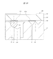
すなわち、ランド接続用コンタクトピン13Lとテスト用ランド115Lとの接触部に着目すると、ランド接続用コンタクトピン13Lの先端部(上端部)の形状は、平坦なテスト用ランド115Lと一点で接触する、いわゆる一本針形状になっている。詳細に説明すると、ランド接続用コンタクトピン13Lの先端部(上端部)の平面形状(図28において、テスト用ランド115L側から見たコンタクトピン13Lの平面形状)は円形から成り、針の頂点はこのランド接続用コンタクトピン13Lの先端部(上端部)の中央部に配置されている。言い換えると、1つの突起がランド接続用コンタクトピン13Lの先端部(上端部)の中央部に形成されている。そのため、ランド接続用コンタクトピン13Lの開口半径(テスト用ランド115Lの周辺部を覆うソルダレジスト106から露出した部分の半径)が上記した許容範囲よりも小さくなると、図29に示すように、両者が非接触状態になるおそれがある。
That is, when attention is paid to the contact portion between the land
これに対し、下面側ランド115には、第1配線基板101の下面よりも下方に突出する半田ボール105が接続されている。また、ボール接続用コンタクトピン13Bの先端部(上端部)の形状は、球状の半田ボール105と多点で接触する、いわゆるクラウン形状になっている。詳細に説明すると、ボール接続用コンタクトピン13Bの先端部(上端部)の平面形状(図28において、下面側ランド115側から見たコンタクトピン13Bの平面形状)が円形から成り、複数の突起はこの先端部の周縁部に沿って配置(形成)されている。そのため、たとえ下面側ランド115や半田ボール105の半径が上記した許容範囲より小さくなった場合でも、半田ボール105とボール接続用コンタクトピン13Bとの非接触は生じ難い。
On the other hand, the
このように、POP型半導体装置の小型化に伴って、第1配線基板101の下面に形成されるランド(下面側ランド115およびテスト用ランド115L)の径が小さくなると、特に、半田ボール105が接続されないテスト用ランド115Lとランド接続用コンタクトピン13Lとの接触不良が発生し易くなり、テスト用ランド115Lを使った第1半導体パッケージ100の電気特性検査を精度よく行うことができなくなる。
As described above, as the diameter of the lands (the lower
本発明の目的は、チップが搭載された配線基板の下面にテスト用ランドを備えた面実装型半導体装置において、配線基板を小型化した場合でも、テスト用ランドを使った電気特性検査を精度よく行う技術を提供することにある。 An object of the present invention is to provide a surface mount semiconductor device having a test land on the lower surface of a wiring board on which a chip is mounted. To provide technology to do.
本発明の他の目的は、チップが搭載された配線基板の下面にテスト用ランドを備えた面実装型半導体装置の小型化を推進する技術を提供することにある。 Another object of the present invention is to provide a technique for promoting the miniaturization of a surface mount semiconductor device having a test land on the lower surface of a wiring board on which a chip is mounted.
本発明の前記ならびにその他の目的と新規な特徴は、本明細書の記述および添付図面から明らかになるであろう。 The above and other objects and novel features of the present invention will be apparent from the description of this specification and the accompanying drawings.
本願において開示される発明のうち、代表的なものの概要を簡単に説明すれば、次のとおりである。
(1)本発明の好ましい一実施形態である半導体装置の製造方法は、第1ランド、前記第1ランドの径よりも大きい径から成る第2ランド、および前記第1ランドに形成され、外部端子と成る導電性部材を有する配線基板と、前記配線基板の前記上面に搭載された半導体チップとを含む組立体を準備する工程と、前記組立体をプローブソケットに装着し、前記プローブソケットの第1コンタクトピンと前記導電性部材とを接触させ、前記プローブソケットの第2コンタクトピンと前記第2ランドとを接触させ、前記組立体の電気特性検査を行う工程とを含む半導体装置の製造方法であって、前記第2ランドには前記導電性部材が接続されず、かつ前記半導体装置の電気特性検査時にのみ使用される。
(2)本発明の好ましい一実施形態である半導体装置は、複数のランドを有する配線基板と、前記配線基板に搭載された半導体チップとを含む半導体装置であって、前記複数のランドは、前記半導体装置の外部端子となる導電性部材が接続された第1ランドと、前記導電性部材が接続されず、かつ前記半導体装置の電気特性検査時にのみ使用される第2ランドとを有し、前記第2ランドの径は、前記第1ランドの径よりも大きい。
Of the inventions disclosed in the present application, the outline of typical ones will be briefly described as follows.
(1) A method of manufacturing a semiconductor device according to a preferred embodiment of the present invention is formed on a first land, a second land having a diameter larger than the diameter of the first land, and the first land, and an external terminal A step of preparing an assembly including a wiring board having a conductive member and a semiconductor chip mounted on the upper surface of the wiring board; and mounting the assembly on a probe socket; A method of manufacturing a semiconductor device, comprising: bringing a contact pin into contact with the conductive member; bringing a second contact pin of the probe socket into contact with the second land; and performing an electrical property test on the assembly; The conductive member is not connected to the second land, and is used only when inspecting the electrical characteristics of the semiconductor device.
(2) A semiconductor device according to a preferred embodiment of the present invention is a semiconductor device including a wiring board having a plurality of lands and a semiconductor chip mounted on the wiring board, wherein the plurality of lands are A first land to which a conductive member serving as an external terminal of the semiconductor device is connected; and a second land to which the conductive member is not connected and is used only at the time of electrical characteristic inspection of the semiconductor device, The diameter of the second land is larger than the diameter of the first land.
本願において開示される発明のうち、代表的なものによって得られる効果を簡単に説明すれば以下の通りである。 The effects obtained by typical ones of the inventions disclosed in the present application will be briefly described as follows.
上記した本発明の好ましい一実施形態によれば、チップが搭載された配線基板の下面にテスト用ランドを備えた面実装型の半導体装置において、配線基板を小型化した場合でも、テスト用ランドを使った電気特性検査を精度よく行うことが可能となる。 According to a preferred embodiment of the present invention described above, in a surface-mount type semiconductor device having a test land on the lower surface of a wiring board on which a chip is mounted, even when the wiring board is downsized, the test land is It is possible to accurately perform the electrical property inspection used.
以下、本発明の実施の形態を図面に基づいて詳細に説明する。なお、実施の形態を説明するための全図において、同一の機能を有する部材には同一の符号を付し、その繰り返しの説明は省略する。また、以下の実施の形態では、特に必要なときを除き、同一または同様な部分の説明を原則として繰り返さない。また、以下の実施の形態を説明する図面においては、構成を分かり易くするために、平面図であってもハッチングを付す場合がある。 Hereinafter, embodiments of the present invention will be described in detail with reference to the drawings. Note that components having the same function are denoted by the same reference symbols throughout the drawings for describing the embodiments, and the repetitive description thereof will be omitted. Also, in the following embodiments, the description of the same or similar parts will not be repeated in principle unless particularly necessary. Further, in the drawings for explaining the following embodiments, hatching may be given even in a plan view for easy understanding of the configuration.
本実施の形態は、コントローラ系チップが搭載された第1半導体パッケージ(第1半導体装置、下段側パッケージ)の上部に、メモリ系チップが搭載された第2半導体パッケージ(第2半導体装置、上段側パッケージ)を積層してシステムを構成するPOP型半導体装置に適用したものである。 In the present embodiment, a second semiconductor package (second semiconductor device, upper stage side) on which a memory system chip is mounted on top of a first semiconductor package (first semiconductor device, lower stage package) on which a controller chip is mounted. This is applied to a POP type semiconductor device in which a package is stacked to constitute a system.
<第1半導体パッケージ(第1半導体装置)>
図1は、POP型半導体装置の第1半導体パッケージを示す平面図、図2は、図1のA−A線に沿った第1半導体パッケージの断面図、図3は、図1のB−B線に沿った第1半導体パッケージの要部拡大断面図である。
<First Semiconductor Package (First Semiconductor Device)>
1 is a plan view showing a first semiconductor package of a POP type semiconductor device, FIG. 2 is a cross-sectional view of the first semiconductor package along the line AA in FIG. 1, and FIG. 3 is a cross-sectional view along line BB in FIG. It is a principal part expanded sectional view of the 1st semiconductor package along a line.
POP型半導体装置の下段側パッケージを構成する第1半導体パッケージ300は、配線基板301と、この配線基板301の上面の中央部に搭載されたコントローラチップ(第1半導体チップ)302とを備えている。
The
配線基板301は、例えばガラスエポキシ樹脂のような汎用樹脂と配線層とを主体として構成された多層配線基板であり、その平面形状は、例えば四角形(正方形)である。配線基板301の上面(表面、主面)には複数の配線310が形成されており、これらの配線310のそれぞれの一端がボンディングリード(電極パッド)311を構成し、他端が上面側ランド(電極パッド)312を構成している。なお、図1は複数の配線310のそれぞれの他端(上面側ランド312)のみを図示している。
The
図3に示すように、配線基板301の上面は、複数の配線310のそれぞれの一端(ボンディングリード311)の表面および他端(上面側ランド312)の表面を除き、配線310を保護するための絶縁性樹脂被膜であるソルダレジスト306によって被覆されている。このソルダレジスト306から露出したボンディングリード311の表面および上面側ランド312の表面には、例えばニッケル(Ni)層の上にAu層を積層した2層の金属膜からなるメッキ層(図示せず)が形成されている。
As shown in FIG. 3, the upper surface of the
配線基板301の下面(裏面)には、複数の下面側ランド(ボール搭載用ランド)315および複数のテスト用ランド315Lが形成されている。下面側ランド315およびテスト用ランド315Lのそれぞれは、配線基板301の内部に形成された複数のビア配線313および複数層(例えば2層)の内部配線314を介して、配線基板301の上面の配線310に電気的に接続されている。すなわち、配線基板301は、その上面の配線310を第1配線層、下面側ランド315およびテスト用ランド315Lを第2配線層、2層の内部配線314を第3および第4配線層とする4層配線基板である。これら4層の配線(配線310、内部配線314、下面側ランド315、テスト用ランド315L)およびそれらを接続するビア配線313は、例えば銅(Cu)のような低抵抗金属からなる。また、配線基板301の下面は、下面側ランド315の表面およびテスト用ランド315Lの表面を除き、ソルダレジスト306によって被覆されている。
A plurality of lower surface lands (ball mounting lands) 315 and a plurality of
配線基板301の下面に形成された下面側ランド315には、半導体装置と外部電子機器との間で信号および電源電位(又は基準電位)の入出力を行うための外部端子(伝導経路)が接続(形成)されている。本実施の形態では、この外部端子は導電性部材から成り、例えば半田ボール(以後、半田ボール305と呼ぶ)である。POP型半導体装置は、これらの半田ボール305をマザーボード(実装基板)の電極パッドと接続し、この半田ボール305を介してディジタルカメラや携帯電話のような外部電子機器のマザーボード(実装基板)に実装される。半田ボール305は、例えば錫(Sn)単体、またはSnに少量のビスマス(Bi)、亜鉛(Zn)、銀(Ag)、Cuのいずれかを添加したSn合金などからなる。
An external terminal (conduction path) for inputting and outputting signals and power supply potential (or reference potential) between the semiconductor device and the external electronic device is connected to the lower
配線基板301の下面に形成されたテスト用ランド315Lは、第1半導体パッケージ(組立体)300の完成後に行われる電気特性検査時にのみ使用される端子である。すなわち、テスト用ランド315Lは、POP型半導体装置を外部電子機器のマザーボードに実装する顧客が使用しない端子である。そのため、テスト用ランド315Lの表面には半田バンプが接続されておらず、平坦なLGA構成となっている。なお、テスト用ランド315Lを使用した第1半導体パッケージ300の電気特性検査については後述する。
The test lands 315L formed on the lower surface of the
配線基板301の上面に搭載されたコントローラチップ302は、平面形状がほぼ正方形の単結晶シリコン基板からなる。このコントローラチップ302は、その主面(集積回路形成面)が配線基板301の上面と対向するように、配線基板301の上面の中央部にフェイスダウン実装されている。コントローラチップ302の主面の周辺部には複数の電極パッド303が形成されている。図示はしないが、これらの電極パッド303の内側のシリコン基板には、第1半導体パッケージ300の上に積層される第2半導体パッケージのメモリチップを制御するための制御回路が形成されている。
The
コントローラチップ302の主面に形成された電極パッド303と、配線基板301の上面に形成された配線310の一端(ボンディングリード311)とは、半田ボール304を介して電気的に接続されている。すなわち、コントローラチップ302は、半田ボール304を介して配線基板301の上面にフリップチップ実装されている。半田ボール304は、配線基板301の下面側ランド315に接続された半田ボール305と同じく、Snに少量のBi、Zn、Ag、Cuを添加したSn合金などからなるが、その融点は半田ボール305のそれよりも高い。
The
配線基板301の上面とコントローラチップ302の主面との間には、コントローラチップ302の主面を保護するためのアンダーフィル樹脂307が充填されている。アンダーフィル樹脂307は、コントローラチップ302と配線基板301との熱膨張係数差に起因して両者の界面に加わる熱応力を緩和する機能も備えている。アンダーフィル樹脂307は、例えば一液型熱硬化性エポキシ樹脂からなる。
An
配線基板301の上面に搭載されたコントローラチップ302の外周近傍には、四角枠状の平面形状を有するダム308が設けられている。コントローラチップ302の周囲を囲むように配置されたこのダム308は、配線基板301の上面とコントローラチップ302の主面との間に液状のアンダーフィル樹脂307を供給した際、このアンダーフィル樹脂307が配線基板301の上面の周辺部に拡散し、配線310の端部(上面側ランド312)の表面を覆うのを防ぐために形成されている。ダム308は、配線基板301の上面を覆うソルダレジスト306と同じ材料(例えばエポキシ樹脂)からなる絶縁性樹脂被膜であり、図3に示すように、ソルダレジスト306の上面に接合されている。
In the vicinity of the outer periphery of the
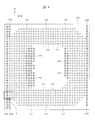
図4は、配線基板301の下面に形成された下面側ランド315およびテスト用ランド315Lのレイアウトを示す平面図である。なお、下面側ランド315に接続されている半田ボール305の図示は省略する。また、下面側ランド315と区別するために、テスト用ランド315Lにはハッチングを付している。
FIG. 4 is a plan view showing a layout of the lower
図4に示すように、下面側ランド315およびテスト用ランド315Lは、配線基板301の下面にアレイ状に配置されている。このうち、下面側ランド315は、配線基板301の中央部から各辺に向かう方向、すなわち図のX方向(配線基板301の一辺に平行な方向)およびこれと直交するY方向に沿って、主として7列に配置されている。一方、テスト用ランド315Lは、主として配線基板301の中央部近傍(下面側ランド列の内側)と最外周部(下面側ランド列の外側)とに配置されている。
As shown in FIG. 4, the lower
図示は省略するが、本実施の形態の第1半導体パッケージ300の上に積層される第2半導体パッケージは、配線基板と、この配線基板の上面に搭載された2枚のメモリチップとを備えている。2枚のメモリチップの一方はDRAMが形成されたチップであり、もう一方はフラッシュメモリが形成されたチップである。
Although not shown, the second semiconductor package stacked on the
そして、配線基板301の下面に形成されたテスト用ランド315Lのうち、配線基板301の中央部近傍(下面側ランド列の内側)に配置されたテスト用ランド315Lは、主としてフラッシュメモリチップインタフェース用ランドを構成している。一方、配線基板301の最外周部(下面側ランド列の外側)に配置されたテスト用ランド315Lは、主としてDRAMチップインタフェース用ランドを構成している。また、配線基板301の内部に形成されたビア配線313のうち、配線基板301の中央部寄りに配置されたビア配線313は、主としてフラッシュメモリチップインタフェース用ビア配線を構成し、配線基板301の外周部寄りに配置された下面側ランド315は、主としてDRAMチップインタフェース用ビア配線を構成している。
Of the test lands 315L formed on the lower surface of the
一般に、DRAMの駆動周波数は、フラッシュメモリの駆動周波数よりも高い。そのため、コントローラチップ302からDRAMチップインタフェース用ランドに至る経路の配線長が長くなると、その分、配線のインピーダンス成分が増加し、かつ配線が不要ノイズを拾う可能性も高くなるので、POP型半導体装置の信頼性(電気特性)が低下する恐れがある。これに対し、上記のように、DRAMチップインタフェース用ランドを配線基板301の最外周部に配置し、かつDRAMチップインタフェース用のビア配線313を配線基板301の外周部寄りに配置した場合は、配線基板301の上面に搭載されたコントローラチップ302からDRAMチップインタフェース用のテスト用ランド315Lに至る経路の配線長が最短化されるので、上記した不具合が回避される。
In general, the driving frequency of DRAM is higher than the driving frequency of flash memory. Therefore, if the wiring length of the path from the
図5は、図4の実線で囲んだ矩形の領域Lを拡大して示す平面図である。図5に示すように、下面側ランド315同士のピッチa1、テスト用ランド315L同士のピッチa2、下面側ランド315とテスト用ランド315Lとのピッチa3は、いずれも同一(a1=a2=a3)であり、例えばそれぞれ0.4mmである。すなわち、下面側ランド315およびテスト用ランド315Lのそれぞれは、X方向およびY方向に沿って、互いに等しいピッチで配置されている。
FIG. 5 is an enlarged plan view showing a rectangular region L surrounded by a solid line in FIG. As shown in FIG. 5, the pitch a1 between the
また、上記X方向およびY方向に沿った下面側ランド315同士の間隔bは、例えばそれぞれ0.1mmである。これに対し、X方向およびY方向に沿ったテスト用ランド315L同士の間隔cは、例えばそれぞれ0.07mmである。すなわち、本実施の形態の配線基板301は、テスト用ランド315Lの直径DLが、下面側ランド315(半田ボール305が接続される外部端子)の直径DBよりも大きい。テスト用ランド315Lの直径DLは、例えば0.33mmであり、下面側ランド315の直径DBは、例えば0.3mmである。テスト用ランド315Lの直径DLを下面側ランド315の直径DBよりも大きくした効果については、後述する。
Moreover, the space | interval b of the lower surface lands 315 along the said X direction and Y direction is each 0.1 mm, for example. On the other hand, the distance c between the test lands 315L along the X direction and the Y direction is, for example, 0.07 mm. That is, in the
<第1半導体パッケージの製造方法>
次に、上記のように構成された第1半導体パッケージ300の製造方法について、図6〜図12を参照しながら説明する。
<Method for Manufacturing First Semiconductor Package>
Next, a method for manufacturing the
図6は、第1半導体パッケージ300の製造に用いるマトリクス基板(大型配線基板)330の上面(表面)を示す平面図、図7は、マトリクス基板330の下面(裏面)を示す平面図、図8は、図6の一部(配線基板2個分の領域)を拡大して示す平面図である。
6 is a plan view showing an upper surface (front surface) of a matrix substrate (large wiring substrate) 330 used for manufacturing the
マトリクス基板330は、前述した配線基板301の導体パターン(配線310、ボンディングリード311、上面側ランド312、ビア配線313、内部配線314、下面側ランド315、テスト用ランド315L)を繰り返し形成した構造を有している。マトリクス基板330は、第1半導体パッケージ300の配線基板301の母体となる基板であり、これをダイシングすることにより、多数(例えば6個)の配線基板301が得られるようになっている。
The
第1半導体パッケージ300を製造するには、まず、図9および図10に示すように、マトリクス基板330の上面にコントローラチップ302を搭載し、あらかじめコントローラチップ302の電極パッド303に接続しておいた半田ボール(バンプ電極)304をボンディングリード311上に位置決めする。続いて、マトリクス基板330を加熱炉内で加熱し、半田ボール304をリフローさせることにより、半田ボール304と電極パッド303とを接続する。
In order to manufacture the
次に、図11および図12に示すように、マトリクス基板330の上面とコントローラチップ302の主面との間に液状のアンダーフィル樹脂307を供給し、続いて、マトリクス基板330を加熱炉内で加熱してアンダーフィル樹脂307を硬化させる。
Next, as shown in FIGS. 11 and 12, a
その後、マトリクス基板330の下面の下面側ランド315に半田ボール305を接続し、続いてマトリクス基板330を加熱炉内で加熱して半田ボール305をリフローさせた後、マトリクス基板330をダイシングすることにより、前記図1〜図3に示した第1半導体パッケージ300が得られる。
Thereafter,
<第1半導体パッケージの電気特性検査>
次に、上記のような方法で製造された第1半導体パッケージ(組立体)300の電気特性検査を行う。図13は、第1半導体パッケージ300の電気特性検査に用いるプローブソケット10の要部を示す概略断面図、図14は、図13に示すプローブソケット10に内蔵されたコンタクトピン(ボール接続用コンタクトピン13Bおよびランド接続用コンタクトピン13L)の要部を示す概略断面図である。
<Inspection of electrical characteristics of first semiconductor package>
Next, the electrical characteristic inspection of the first semiconductor package (assembly) 300 manufactured by the above method is performed. 13 is a schematic cross-sectional view showing the main part of the
図13に示すように、プローブソケット10は、ソケット本体11と、このソケット本体11に開閉可能に取り付けられたキャップ12とを備えており、ソケット本体11には、複数個のボール接続用コンタクトピン13Bと複数個のランド接続用コンタクトピン13Lとが内蔵されている。
As shown in FIG. 13, the
ボール接続用コンタクトピン(第1コンタクトピン)13Bは、第1半導体パッケージ300の配線基板301の下面側ランド315に取り付けられた半田ボール305と接触するプローブ針であり、ランド接続用コンタクトピン13Lは、テスト用ランド315Lと接触するプローブ針である。ボール接続用コンタクトピン13Bの数は、配線基板301の下面に形成された下面側ランド315の数と同じであり、ランド接続用コンタクトピン(第2コンタクトピン)13Lの数は、テスト用ランド315Lの数と同じである。
The ball connection contact pin (first contact pin) 13B is a probe needle that comes into contact with the
図14に示すように、ボール接続用コンタクトピン13Bとランド接続用コンタクトピン13Lのそれぞれは、金属製の管の中に収納されたコイルバネ14の弾性力によってピンガイド15内を上下動するポゴピン(POGO pin)構造を有している。また、ボール接続用コンタクトピン13Bとランド接続用コンタクトピン13Lのそれぞれの下端部は、ソケット本体11に内蔵された図示しないコンタクトプローブに接続されている。このとき、図14に示すように、それぞれのコンタクトピン13B,13Lは、それぞれのピンガイド15内において上下動を可能とするために、ピンガイド15の内壁面とコンタクトピン13B,13Lの表面との間に隙間が設けられている。
As shown in FIG. 14, each of the ball connection contact pin 13 </ b> B and the land connection contact pin 13 </ b> L is a pogo pin that moves up and down in the
ボール接続用コンタクトピン13Bの先端部(上端部)の形状は、球状の半田ボール305と多点で接触する、いわゆるクラウン形状になっている。詳細に説明すると、ボール接続用コンタクトピン13Bの先端部(上端部)の平面形状(図28において、下面側ランド115側から見たコンタクトピン13Bの平面形状)が円形から成り、複数の突起はこの先端部の周縁部に沿って配置(形成)されている。このように、ボール接続用コンタクトピン13Bの先端部(上端部)の形状を、所謂、クラウン形状にすることで、球状の半田ボール(バンプ電極)305との接触点(接触面積)を増やすことができる。一方、ランド接続用コンタクトピン13Lの先端部(上端部)の形状は、平坦なテスト用ランド315Lと一点で接触する、いわゆる一本針形状になっている。詳細に説明すると、ランド接続用コンタクトピン13Lの先端部(上端部)の平面形状(図28において、テスト用ランド115L側から見たコンタクトピン13Lの平面形状)は円形から成り、針の頂点はこのランド接続用コンタクトピン13Lの先端部(上端部)の中央部に配置されている。言い換えると、1つの突起がランド接続用コンタクトピン13Lの先端部(上端部)の中央部に形成されている。なお、図に示したボール接続用コンタクトピン13Bの先端部は、半田ボール305と2点で接触する形状になっているが、半田ボール305と3点以上で接触する形状であってもよいことは勿論である。
The shape of the tip (upper end) of the ball
上記プローブソケット10を使用して第1半導体パッケージ300の電気特性検査を行う際は、図15に示すように、第1半導体パッケージ300をソケット本体11の上面に位置決めし、配線基板301の上面を上方からキャップ12で押さえ付けることによって、ソケット本体11の上面に固定する。詳細に説明すると、図15に示すように、ソケット本体11の上面には、凹部(収納部)が形成されており、第1半導体パッケージ300の下面がこのソケット本体11の凹部における底面と対向するように、第1半導体パッケージ300をこのソケット本体11の凹部内に配置する。
When the electrical characteristics inspection of the
このように、第1半導体パッケージ300の電気特性検査を行う間、配線基板301の上面を上方からキャップ12で押さえ付けておくことにより、配線基板301上に搭載されたコントローラチップ302の発熱などに起因する配線基板301の反りが抑制される。これにより、配線基板301の反りに起因するランド(下面側ランド315およびテスト用ランド315L)とプローブ針(ボール接続用コンタクトピン13Bおよびランド接続用コンタクトピン13L)との位置合わせ精度の低下を抑制することができる。
As described above, during the electrical characteristic inspection of the
また、配線基板301の上面をキャップ12で押さえ付ける際には、キャップ12との接触による配線基板301の上面の損傷を防ぐために、キャップ12の下面に平坦な底面を有する凸部12aを設け、この凸部12aの底面を配線基板301の上面に形成されたダム308と接触させる。図15には示さないが、この凸部12aは、配線基板301の上面のダム308と同様、四角枠状の平面形状を有している。
Further, when pressing the upper surface of the
図16は、キャップ12の凸部12aと配線基板301のダム308との接触部を示す拡大断面図である。図16に示すように、ダム308の幅は、キャップ12の下面に設けられた凸部12aとダム308とが接触する領域、すなわち凸部12aの底面の幅よりも広くすることが望ましい。このようにすると、凸部12aの底面全体がダム308の上面と接触するので、ダム308の上面に対して均等な押圧力を印加することができる。他方、ダム308の幅を凸部12aの幅よりも狭くした場合には、凸部12aの底面の一部がダム308の上面と非接触になり、ダム308の上面に印加される押圧力が不均等になることがある。
FIG. 16 is an enlarged cross-sectional view showing a contact portion between the
また、配線基板301の上面にダム308を設ける際には、配線基板301の上面において、配線基板301の中央部から一辺に向かう方向に沿って複数列に亘って配列された半田ボール列の中央部(中央近傍)と平面的に重なる位置にダム308を配置することが望ましい。図16に示す例では、7列に配置された半田ボール列の中央に位置する半田ボール305の上方にダム308を配置している。これにより、キャップ12の凸部12aおよび配線基板301を介して複数の半田ボール列のそれぞれに印加される押圧力をほぼ均等にすることができる。
Further, when the
前述したように、配線基板301の上面にダム308を設ける目的の一つは、配線基板301の上面とコントローラチップ302の主面との間に供給した液状のアンダーフィル樹脂307が配線基板301の周辺部に広がることを防止することにある。そのため、例えば図17に示すように、アンダーフィル樹脂307の広がり防止効果を高める目的で、コントローラチップ302の周囲を2つのダム308a、308bで二重に囲む場合もある。この場合においても、図18に示すように、2つのダム308a、308bの幅を凸部12aの幅をよりも広くし、凸部12aの底面全体をダム308a、308bの上面と接触させることにより、ダム308a、308bの上面に対して均等な押圧力を印加することができる。
As described above, one of the purposes of providing the
なお、前述した第1半導体パッケージ300の製造方法において、マトリクス基板330の上面とコントローラチップ302の主面との間に液状のアンダーフィル樹脂307を供給する工程(図11、図12参照)では、コントローラチップ302とその周囲を囲むダム308との狭い隙間にディスペンサノズルの先端を挿入し、コントローラチップ302の一辺または二辺に沿ってディスペンサノズルを移動させながらアンダーフィル樹脂307を供給する。そのため、ダム308の幅を前述した凸部12aの幅よりも広くすると、コントローラチップ302とダム308との隙間がさらに狭くなり、この隙間にディスペンサノズルの先端を挿入することができなくなる場合がある。このような場合は、コントローラチップ302を囲むダム308の四辺のうち、対向する二辺のみ幅を広くしてもよい。
In the method of manufacturing the
また、ダム308の外側の領域には、配線310の一端を構成する複数の上面側ランド312が配置されているが、上面側ランド312の数によってはダム308の幅を広げることが困難が場合がある。このような場合も、コントローラチップ302を囲むダム308の四辺のうち、対向する二辺のみ幅を広くすればよい。
In addition, a plurality of upper surface lands 312 constituting one end of the
図19は、配線基板301の下面側ランド315に接続された半田ボール305とボール接続用コンタクトピン13Bとの接触部、およびテスト用ランド315Lとランド接続用コンタクトピン13Lとの接触部を示す概略断面図である。
FIG. 19 schematically shows a contact portion between the
ここで、各部材の寸法の一例を示すと、下面側ランド315の直径DBおよびテスト用ランド315Lの直径DLは、前述したように、例えばDB=0.3mmおよびDL=0.33mmである。また、テスト用ランド315Lおよび下面側ランド315のそれぞれの周辺部はソルダレジスト306で覆われているので、実際に配線基板301の下面に露出している領域の径を開口径と定義すると、下面側ランド315の開口径DBSは、例えば0.23mmであり、テスト用ランド315Lの開口径DLSは、例えば0.27mmである。
Here, as an example of the dimensions of each member, the diameter DB of the lower
一方、ボール接続用コンタクトピン13Bとランド接続用コンタクトピン13Lのそれぞれの直径D1は、例えば0.15mmであり、ピンガイド15の直径D2は、例えば0.19mmである。また、ボール接続用コンタクトピン13Bが挿入されるピンガイド15の先端部近傍(ボールガイド16)の直径D3は、半田ボール305の径を例えば0.25mmとしたとき、例えば0.35mmである。
On the other hand, the diameter D1 of each of the ball
ここで、ボール接続用コンタクトピン13Bと半田ボール305との位置ずれ量、およびランド接続用コンタクトピン13Lとテスト用ランド315Lとの位置ずれ量がいずれも0である場合には、図19に示すように、ボール接続用コンタクトピン13Bの中心が半田ボール305の中心と一致し、ランド接続用コンタクトピン13Lの中心がテスト用ランド315Lの中心と一致する。
Here, when both the positional displacement amount between the ball
しかし、実際の配線基板301の下面に形成された下面側ランド315の位置およびテスト用ランド315Lの位置は、配線基板301の加工ばらつきのために、設計上の位置からずれていることがある。同様に、実際のソケット本体11に設けられたボール接続用コンタクトピン13Bの位置およびランド接続用コンタクトピン13Lの位置は、ソケット本体11の加工ばらつきのために、設計上の位置からずれていることがある。さらに、第1半導体パッケージ300をプローブソケット10に装着して電気特性検査を行うと、配線基板301に搭載されたコントローラチップ302の発熱のために、配線基板301に反りが発生し、特に配線基板301の周辺部近傍において、ボール接続用コンタクトピン13Bと半田ボール305との位置ずれ、およびランド接続用コンタクトピン13Lとテスト用ランド315Lとの位置ずれが発生する。
However, the position of the lower
そのため、POP型半導体装置の小型化に伴って配線基板301の外形寸法が小さくなり、配線基板301の下面に形成されるランド(下面側ランド315およびテスト用ランド315L)の径およびランド間ピッチが小さくなると、前述したように、特に、半田ボール305が接続されていないテスト用ランド315Lとランド接続用コンタクトピン13Lとの間に接触不良が発生し易くなる。
Therefore, as the POP type semiconductor device is miniaturized, the outer dimensions of the
そこで、本実施の形態の第1半導体パッケージ300は、配線基板301の下面に形成されたテスト用ランド315Lの直径DLを下面側ランド315の直径DBより大きくしている。これにより、テスト用ランド315Lの開口径DLSも下面側ランド315の開口径DBSより大きくなるので、配線基板301の外形寸法が縮小され、ランド(下面側ランド315およびテスト用ランド315L)の径およびランド間ピッチが小さくなっても、テスト用ランド315Lとランド接続用コンタクトピン13Lとの接触不良の発生を抑制することができる。
Therefore, in the
図20は、上記した配線基板301およびソケット本体11の加工ばらつきや、配線基板301に反りなどによって、ランド接続用コンタクトピン13Lとテスト用ランド315Lの位置ずれ量が最大になった状態を示している。そこで、この状態におけるテスト用ランド315Lの中心からランド接続用コンタクトピン13Lの先端までの距離を上記した位置ずれ量の最大値Sと定義すると、テスト用ランド315Lの開口部の半径(DLS/2)を位置ずれ量の最大値Sよりも大きくすることにより、テスト用ランド315Lとランド接続用コンタクトピン13Lとの非接触を確実に防止することができる。
FIG. 20 shows a state in which the positional displacement amount between the land
なお、下面側ランド315に接続された半田ボール305は、配線基板301の下面よりも下方に突出しており、かつボール接続用コンタクトピン13Bの先端部(上端部)の形状は、球状の半田ボール305と多点で接触する、いわゆるクラウン形状になっている。そのため、たとえ半田ボール305の開口部の半径(DBS/2)が上記した位置ずれ量の最大値Sより小さくなった場合でも、両者が非接触状態になることはない。
The
次に、この状態で第1半導体パッケージ300に対する各種の電気特性検査を行う。この電気特性検査は、例えば配線基板301上のコントローラチップ302からテスト用ランド315Lに至る配線経路の導通/非導通を確認する検査、コントローラチップ302に対するAC/DCテスト、コントローラチップ302から半田ボール305に至る配線経路の導通/非導通を確認する検査などを含んでいる。
Next, in this state, various electrical characteristic inspections are performed on the
本実施の形態によれば、POP型半導体装置の小型化に伴って配線基板301の外形寸法が小さくなった場合でも、テスト用ランド315Lを使った第1半導体パッケージ300の電気特性検査を精度よく行うことができるので、POP型半導体装置の小型化を推進することができる。
According to the present embodiment, even when the external dimensions of the
このようにして、前記マトリクス基板330から取得した複数個の第1半導体パッケージ(組立体)300のそれぞれに対して上記の電気特性検査を行い、良品の第1半導体パッケージ300を選別した後、良品の第1半導体パッケージ300上に、例えば前記図25〜図27に示した第2半導体パッケージ(組立体)200を積層することによって、本実施の形態のPOP型半導体装置を取得することができる。
In this way, the above-described electrical characteristic inspection is performed on each of the plurality of first semiconductor packages (assemblies) 300 obtained from the
図21は、組み立てが完了したPOP型半導体装置の全体構成を示す断面図である。POP型半導体装置の第1半導体パッケージ300上に積層する第2半導体パッケージ200の構成については前述したので、その繰り返しの説明は省略する。また、第2半導体パッケージ200を第1半導体パッケージ300上に積層する方法は、第2半導体パッケージ200を前述した第1半導体パッケージ100上に積層する方法と同じでよいので、その説明は省略する。
FIG. 21 is a cross-sectional view showing the overall configuration of a POP type semiconductor device that has been assembled. Since the configuration of the
なお、上記POP型半導体装置の組み立て方法としては、半導体製造メーカが第1半導体パッケージ300上に第2半導体パッケージ200を積層し、完成品として出荷する方式と、半導体製造メーカから第1半導体パッケージ300を購入した顧客が、電子機器製品の用途に応じて選定した第2パッケージ200を第1半導体パッケージ300上に積層する方式とがある。
As a method for assembling the POP type semiconductor device, a method in which a semiconductor manufacturer stacks the
以上、本発明者によってなされた発明を実施の形態に基づき具体的に説明したが、本発明は前記実施の形態に限定されるものではなく、その要旨を逸脱しない範囲で種々変更可能であることはいうまでもない。 As mentioned above, the invention made by the present inventor has been specifically described based on the embodiment. However, the present invention is not limited to the embodiment, and various modifications can be made without departing from the scope of the invention. Needless to say.
例えば、前記実施の形態では、第1半導体パッケージ300の配線基板301の上面に搭載されたコントローラチップ302は、導電性部材として、半田ボール(バンプ電極)304を介して配線基板301の電極パッドと電気的に接続したが、ワイヤを介して配線基板301の電極パッドと電気的に接続してもよい。なお、ワイヤの材料は、例えば金(Au)である。
For example, in the above embodiment, the
また、図22に示すように、配線基板301の下面に形成されるテスト用ランド315Lの平面形状を四角形にしてもよい。図22には示さないが、この場合は、ソルダレジストで覆われていないテスト用ランド315Lの開口形状も四角形にする。例えばテスト用ランド315Lの平面形状を正方形にした場合は、この正方形の一辺と同じ長さの直径を有する円に比べて面積が約1.27倍増加する(図22の斜線を付した部分)ので、テスト用ランド315Lとランド接続用コンタクトピン13Lとの接触不良の発生をさらに有効に抑制することができる。
Further, as shown in FIG. 22, the planar shape of the
また、前記実施の形態の第1半導体パッケージ300は、配線基板301の上面にコントローラチップ302をフリップチップ実装したが、例えば図23および図24に示すように、配線基板301の上面に接着剤320を介してコントローラチップ302をフェイスアップ実装し、コントローラチップ302の主面の電極パッド303と配線基板301の上面のボンディングリード311をAuワイヤ321で電気的に接続してもよい。この場合は、コントローラチップ302、Auワイヤ321およびボンディングリード311を樹脂封止体322で封止する。
In the
前記実施の形態は、POP型半導体装置に適用したものであるが、本発明は、例えばSiP(システムインパッケージ)型の半導体装置に適用してもよい。さらには、図30に示すように、配線基板301の上面には、配線基板301の上面に搭載されるチップ(例えばコントローラチップ302)の電極パッド(ボンディングパッド)303と電気的に接続される電極パッド(ボンディングリード311)しか形成されていない。言い換えると、配線基板301の上面に第2半導体パッケージ200と電気的に接続される電極パッド(上面側ランド312)が形成されていない、所謂、BGA(ボールグリッドアレイ)といった面実装パッケージ形態を有する他の半導体装置にも適用することができる。この理由として、本願発明は、上記したように、外部端子となる半田ボール305が接続される下面側ランド(第1ランド)315と、外部端子となる半田ボール305が接続されず、かつ半導体装置(組立体)の電気特性検査時にのみ使用されるテスト用ランド(第2ランド)315Lとを有する配線基板301を備えた組立体の電気特性検査を行う際に生じる課題について対策するものである。すなわち、前記実施の形態は、半導体装置の小型化が進み、各ランド(315、315L)の径が小さくなると、プローブ針とランドとの位置合わせ精度が低下し、最悪の場合、プローブ針とランドとが非接触となるために、正確な電気特性検査を行うことができなくなるという問題に着目したものであるため、POP型の半導体装置に限られるものではない。
Although the above embodiment is applied to a POP type semiconductor device, the present invention may be applied to, for example, a SiP (system in package) type semiconductor device. Furthermore, as shown in FIG. 30, on the upper surface of the
本発明は、チップが搭載された配線基板の下面に設けたテスト用ランドを使用して電気特性検査を行う面実装パッケージ型の半導体装置に適用することができる。 The present invention can be applied to a surface-mount package type semiconductor device that performs electrical characteristic inspection using a test land provided on the lower surface of a wiring board on which a chip is mounted.
10 プローブソケット
11 ソケット本体
12 キャップ
12a 凸部
13B ボール接続用コンタクトピン(第1コンタクトピン)
13L ランド接続用コンタクトピン(第2コンタクトピン)
14 コイルバネ
15 ピンガイド
16 ボールガイド
100 第1半導体パッケージ
101 第1配線基板
102 コントローラチップ
103 電極パッド
104 半田ボール
105 半田ボール
106 ソルダレジスト
107 アンダーフィル樹脂
110 配線
111 ボンディングリード(電極パッド)
112 上面側ランド(電極パッド)
115 下面側ランド(ボール搭載用ランド)
115L テスト用ランド
200 第2半導体パッケージ(組立体)
201 第2配線基板
202 DRAMチップ
203 フラッシュメモリチップ
204 電極パッド
205 電極パッド
206 Auワイヤ
207 Auワイヤ
208 半田ボール(外部端子)
211 ボンディングリード
212 ビア配線
213 下面側ランド
220 接着剤
221 樹脂封止体
300 第1半導体パッケージ(組立体、第1半導体装置、下段側パッケージ)
301 配線基板
302 コントローラチップ
303 電極パッド
304 半田ボール(バンプ電極)
305 半田ボール(外部端子)
306 ソルダレジスト
307 アンダーフィル樹脂
308、308a、308b ダム
310 配線
311 ボンディングリード
312 上面側ランド
313 ビア配線
314 内部配線
315 下面側ランド
315L テスト用ランド
320 接着剤
321 Auワイヤ
322 樹脂封止体
330 マトリクス基板(大型配線基板)
DESCRIPTION OF
13L Land connection contact pin (second contact pin)
14
112 Upper surface side land (electrode pad)
115 Lower side land (land for ball mounting)
201
211
301 Wiring
305 Solder ball (external terminal)
306 Solder resist 307
Claims (7)
(a)上面、前記上面に形成された第1電極パッド、前記上面に形成された第2電極パッド、前記上面とは反対側の下面、前記下面に形成され、かつ前記第1電極パッドと電気的に接続された第1ランド、前記下面に形成され、かつ前記第2電極パッドと電気的に接続され、かつ前記第1ランドの径よりも大きい径から成る第2ランド、前記第1ランドおよび前記第2ランドのそれぞれの表面を露出するように前記下面に形成された絶縁性樹脂被膜、および前記第1ランドの前記表面に形成された外部端子と成る導電性部材を有する配線基板と、前記配線基板の前記上面に搭載された半導体チップとを含む組立体を準備する工程;
(b)前記組立体をプローブソケットに装着し、前記プローブソケットの第1コンタクトピンと前記導電性部材とを接触させ、前記プローブソケットの第2コンタクトピンと前記第2ランドとを接触させ、前記組立体の電気特性検査を行う工程;
ここで、
前記第2ランドの前記表面には外部端子と成る導電性部材が接続されず、前記第2ランドの前記表面は露出している。 A method for manufacturing a semiconductor device comprising the following steps:
(A) an upper surface, a first electrode pad formed on the upper surface, a second electrode pad formed on the upper surface, a lower surface opposite to the upper surface, formed on the lower surface, and electrically connected to the first electrode pad Connected first lands, formed on the lower surface and electrically connected to the second electrode pad and having a diameter larger than the diameter of the first land , the first land, a wiring substrate having the lower surface formed insulating resin film, and the first land conductive member comprising an external terminal formed on the surface of the to expose the surface of each of the second lands, the Preparing an assembly including a semiconductor chip mounted on the upper surface of the wiring board;
(B) mounting the assembly on a probe socket; bringing the first contact pin of the probe socket into contact with the conductive member; bringing the second contact pin of the probe socket into contact with the second land; Conducting electrical property inspection of
here,
Not connected conductive member comprising an external pin to the surface of the second land, the surface of the second land is exposed.
前記第1コンタクトピンの前記先端部の周縁部に沿って複数の突起が形成されており、
前記第2コンタクトピンの先端部の平面形状は円形から成り、
前記第2コンタクトピンの前記先端部の中央部に一つの突起が形成されていることを特徴とする請求項1記載の半導体装置の製造方法。 The planar shape of the tip of the first contact pin is a circle,
A plurality of protrusions are formed along a peripheral edge portion of the tip portion of the first contact pin,
The planar shape of the tip of the second contact pin is a circle,
2. The method of manufacturing a semiconductor device according to claim 1, wherein one protrusion is formed at a central portion of the tip portion of the second contact pin.
前記第1コンタクトピンは、前記第1ピンガイド内に配置されており、
前記第2コンタクトピンは、前記第2ピンガイド内に配置されており、
前記第1および第2コンタクトピンの表面と、前記第1および第2ピンガイドの内壁面との間には隙間が形成され、
前記(b)工程では、前記配線基板の前記下面が前記ソケット本体の凹部の底面と対向し、かつ前記導電性部材が前記ボールガイド内に位置するように、前記組立体を前記凹部内に収納することを特徴とする請求項2記載の半導体装置の製造方法。 The probe socket has a socket body including a first pin guide, a ball guide connected to the first pin guide, and the second pin guide.
The first contact pin is disposed in the first pin guide;
The second contact pin is disposed in the second pin guide;
A gap is formed between the surfaces of the first and second contact pins and the inner wall surfaces of the first and second pin guides,
In the step (b), the assembly is housed in the recess so that the lower surface of the wiring board faces the bottom surface of the recess of the socket body and the conductive member is positioned in the ball guide. The method of manufacturing a semiconductor device according to claim 2, wherein:
前記配線基板の平面形状は四角形から成り、
前記第1ランドは、前記配線基板の前記下面における中央部から、前記配線基板の前記下面における第1辺に向かう方向に沿って複数列に亘って配列されており、
前記ダムは、前記配線基板の前記上面において、複数列に亘って配列された複数の第1ランド列の中央部と平面的に重なる位置に配置され、
前記(b)工程では、前記プローブソケットのキャップに設けられた凸部を前記ダムに押し付けることによって、前記プローブソケットの前記第1コンタクトピンと前記導電性部材とを接触させ、前記プローブソケットの前記第2コンタクトピンと前記第2ランドとを接触させ、前記組立体の電気特性検査を行うことを特徴とする請求項3記載の半導体装置の製造方法。 On the upper surface of the wiring board, a dam is formed around the semiconductor chip,
The planar shape of the wiring board is a quadrangle,
The first lands are arranged in a plurality of rows along a direction from a central portion on the lower surface of the wiring board toward a first side on the lower surface of the wiring board,
The dam is disposed on the upper surface of the wiring board at a position overlapping in plan with the central portions of the plurality of first land rows arranged over a plurality of rows,
In step (b), by pressing the convex portion provided on the cap of the probe socket to the dam, the first contact pins of the probe socket and into contact with said conductive member, said the probe socket first 4. The method of manufacturing a semiconductor device according to claim 3, wherein two electrical contact pins and the second land are brought into contact with each other to inspect the electrical characteristics of the assembly.
前記複数のランドは、前記半導体装置の外部端子となる導電性部材が表面に接続された第1ランドと、外部端子となる導電性部材が表面に接続されず、前記表面が露出した第2ランドとを有し、
前記第2ランドの径は、前記第1ランドの径よりも大きいことを特徴とする半導体装置。 Upper surface, a plurality of electrode pads formed on the upper surface, a lower surface opposite the upper surface, is formed prior Symbol lower surface, said plurality of electrode pads respectively electrically connected to a plurality of lands, and the plurality of A semiconductor device comprising: a wiring board having an insulating resin film formed on the lower surface so as to expose each surface of a land; and a semiconductor chip mounted on the upper surface of the wiring board,
The plurality of lands include a first land in which a conductive member to be an external terminal of the semiconductor device is connected to the surface, and a second land in which the conductive member to be an external terminal is not connected to the surface and the surface is exposed . And
The diameter of the second land is larger than the diameter of the first land.
Priority Applications (2)
| Application Number | Priority Date | Filing Date | Title |
|---|---|---|---|
| JP2009280469A JP5342422B2 (en) | 2009-12-10 | 2009-12-10 | Semiconductor device and manufacturing method thereof |
| US12/946,131 US8404497B2 (en) | 2009-12-10 | 2010-11-15 | Semiconductor device and method of manufacturing the same |
Applications Claiming Priority (1)
| Application Number | Priority Date | Filing Date | Title |
|---|---|---|---|
| JP2009280469A JP5342422B2 (en) | 2009-12-10 | 2009-12-10 | Semiconductor device and manufacturing method thereof |
Publications (3)
| Publication Number | Publication Date |
|---|---|
| JP2011122924A JP2011122924A (en) | 2011-06-23 |
| JP2011122924A5 JP2011122924A5 (en) | 2012-10-11 |
| JP5342422B2 true JP5342422B2 (en) | 2013-11-13 |
Family
ID=44141913
Family Applications (1)
| Application Number | Title | Priority Date | Filing Date |
|---|---|---|---|
| JP2009280469A Active JP5342422B2 (en) | 2009-12-10 | 2009-12-10 | Semiconductor device and manufacturing method thereof |
Country Status (2)
| Country | Link |
|---|---|
| US (1) | US8404497B2 (en) |
| JP (1) | JP5342422B2 (en) |
Families Citing this family (12)
| Publication number | Priority date | Publication date | Assignee | Title |
|---|---|---|---|---|
| EP2503594A1 (en) * | 2011-03-21 | 2012-09-26 | Dialog Semiconductor GmbH | Signal routing optimized IC package ball/pad layout |
| CN102858096B (en) * | 2012-09-12 | 2015-04-08 | 梁锦贤 | Device for SMT (surface mount technology) preprocessing of POP (package on package) devices |
| KR101474611B1 (en) * | 2012-10-30 | 2014-12-18 | 삼성전기주식회사 | System and method for analyzing of defect position |
| US9362187B2 (en) * | 2013-01-18 | 2016-06-07 | Infineon Technologies Ag | Chip package having terminal pads of different form factors |
| US8941224B2 (en) * | 2013-03-29 | 2015-01-27 | Kinsus Interconnect Technology Corp. | Package structure of a chip and a substrate |
| US9263409B2 (en) * | 2013-05-21 | 2016-02-16 | Esilicon Corporation | Mixed-sized pillars that are probeable and routable |
| KR101535179B1 (en) * | 2014-12-03 | 2015-07-08 | 재단법인 서울테크노파크 | Contactor of test socket for semiconductor device and method of manufacturing the same |
| KR20160119942A (en) * | 2015-04-06 | 2016-10-17 | 에스케이하이닉스 주식회사 | Semiconductor package with socket plug interconnection |
| US10460957B2 (en) * | 2017-01-31 | 2019-10-29 | Skyworks Solutions, Inc. | Control of under-fill using an encapsulant for a dual-sided ball grid array package |
| JP2018163087A (en) * | 2017-03-27 | 2018-10-18 | ルネサスエレクトロニクス株式会社 | Semiconductor device manufacturing method, semiconductor device inspection apparatus, and semiconductor device |
| JP6848733B2 (en) * | 2017-07-10 | 2021-03-24 | 三菱電機株式会社 | Energization test socket and energization test method |
| EP3837611A4 (en) * | 2018-08-14 | 2022-05-11 | Rambus Inc. | Packaged integrated device |
Family Cites Families (8)
| Publication number | Priority date | Publication date | Assignee | Title |
|---|---|---|---|---|
| JP2001116795A (en) * | 1999-10-18 | 2001-04-27 | Mitsubishi Electric Corp | Test socket and connection sheet for use in test socket |
| JP2001318119A (en) * | 2000-05-02 | 2001-11-16 | Fujitsu Ltd | Connection method for ic package and ic contactor |
| JP4854148B2 (en) * | 2001-08-28 | 2012-01-18 | 富士通セミコンダクター株式会社 | Semiconductor device |
| JP4601365B2 (en) * | 2004-09-21 | 2010-12-22 | ルネサスエレクトロニクス株式会社 | Semiconductor device |
| JP2008070146A (en) * | 2006-09-12 | 2008-03-27 | Yokowo Co Ltd | Socket for inspection |
| JP5144170B2 (en) | 2007-08-20 | 2013-02-13 | ルネサスエレクトロニクス株式会社 | Mounting method of semiconductor device |
| JP5043563B2 (en) * | 2007-08-29 | 2012-10-10 | 新光電気工業株式会社 | Wiring board and manufacturing method thereof |
| JP2009200101A (en) * | 2008-02-19 | 2009-09-03 | Liquid Design Systems:Kk | Semiconductor chip and semiconductor device |
-
2009
- 2009-12-10 JP JP2009280469A patent/JP5342422B2/en active Active
-
2010
- 2010-11-15 US US12/946,131 patent/US8404497B2/en active Active
Also Published As
| Publication number | Publication date |
|---|---|
| US8404497B2 (en) | 2013-03-26 |
| JP2011122924A (en) | 2011-06-23 |
| US20110140105A1 (en) | 2011-06-16 |
Similar Documents
| Publication | Publication Date | Title |
|---|---|---|
| JP5342422B2 (en) | Semiconductor device and manufacturing method thereof | |
| US8125792B2 (en) | Substrate for wiring, semiconductor device for stacking using the same, and stacked semiconductor module | |
| JP4473807B2 (en) | Multilayer semiconductor device and lower layer module of multilayer semiconductor device | |
| US9129914B2 (en) | Electronic device, test board, and semiconductor device manufacturing method | |
| US9230938B2 (en) | Method of manufacturing semiconductor device | |
| US20050248011A1 (en) | Flip chip semiconductor package for testing bump and method of fabricating the same | |
| US20150123690A1 (en) | Probe card | |
| JP2010093109A (en) | Semiconductor device, method of manufacturing the same, and method of manufacturing semiconductor module | |
| JPH10229142A (en) | Ball grid array package | |
| US20090261465A1 (en) | Semiconductor device and its manufacturing method | |
| TW201705413A (en) | Semiconductor apparatus | |
| JP3692978B2 (en) | Wiring board manufacturing method | |
| US6507118B1 (en) | Multi-metal layer circuit | |
| JP5666366B2 (en) | Manufacturing method of semiconductor device | |
| US7576551B2 (en) | Test socket and test board for wafer level semiconductor testing | |
| JP4737995B2 (en) | Semiconductor device | |
| KR101169687B1 (en) | Bump for mounting semiconductor chip and semiconductor chip including the same and electrical test method thereof | |
| JP2010093106A (en) | Semiconductor device and method for manufacturing the same | |
| JP2010157561A (en) | Semiconductor device and semiconductor system | |
| JP3895465B2 (en) | Board mounting method, board mounting structure | |
| JP2001223325A (en) | Semiconductor device | |
| JP4374251B2 (en) | Semiconductor device | |
| JP2010212537A (en) | Semiconductor device | |
| KR100900229B1 (en) | Fine-pitch ball grid array package | |
| JP2018059866A (en) | Semiconductor device manufacturing method and semiconductor device |
Legal Events
| Date | Code | Title | Description |
|---|---|---|---|
| A521 | Request for written amendment filed |
Free format text: JAPANESE INTERMEDIATE CODE: A523 Effective date: 20120827 |
|
| A621 | Written request for application examination |
Free format text: JAPANESE INTERMEDIATE CODE: A621 Effective date: 20120827 |
|
| A977 | Report on retrieval |
Free format text: JAPANESE INTERMEDIATE CODE: A971007 Effective date: 20130628 |
|
| TRDD | Decision of grant or rejection written | ||
| A01 | Written decision to grant a patent or to grant a registration (utility model) |
Free format text: JAPANESE INTERMEDIATE CODE: A01 Effective date: 20130716 |
|
| A61 | First payment of annual fees (during grant procedure) |
Free format text: JAPANESE INTERMEDIATE CODE: A61 Effective date: 20130809 |
|
| A977 | Report on retrieval |
Free format text: JAPANESE INTERMEDIATE CODE: A971007 Effective date: 20130814 |
|
| R150 | Certificate of patent or registration of utility model |
Ref document number: 5342422 Country of ref document: JP Free format text: JAPANESE INTERMEDIATE CODE: R150 Free format text: JAPANESE INTERMEDIATE CODE: R150 |
|
| S531 | Written request for registration of change of domicile |
Free format text: JAPANESE INTERMEDIATE CODE: R313531 |
|
| R350 | Written notification of registration of transfer |
Free format text: JAPANESE INTERMEDIATE CODE: R350 |