JP5144170B2 - Mounting method of semiconductor device - Google Patents
Mounting method of semiconductor device Download PDFInfo
- Publication number
- JP5144170B2 JP5144170B2 JP2007213554A JP2007213554A JP5144170B2 JP 5144170 B2 JP5144170 B2 JP 5144170B2 JP 2007213554 A JP2007213554 A JP 2007213554A JP 2007213554 A JP2007213554 A JP 2007213554A JP 5144170 B2 JP5144170 B2 JP 5144170B2
- Authority
- JP
- Japan
- Prior art keywords
- semiconductor device
- terminal
- connection
- circuit
- bumps
- Prior art date
- Legal status (The legal status is an assumption and is not a legal conclusion. Google has not performed a legal analysis and makes no representation as to the accuracy of the status listed.)
- Expired - Fee Related
Links
Images


Classifications
-
- H—ELECTRICITY
- H01—ELECTRIC ELEMENTS
- H01L—SEMICONDUCTOR DEVICES NOT COVERED BY CLASS H10
- H01L2224/00—Indexing scheme for arrangements for connecting or disconnecting semiconductor or solid-state bodies and methods related thereto as covered by H01L24/00
- H01L2224/01—Means for bonding being attached to, or being formed on, the surface to be connected, e.g. chip-to-package, die-attach, "first-level" interconnects; Manufacturing methods related thereto
- H01L2224/10—Bump connectors; Manufacturing methods related thereto
- H01L2224/15—Structure, shape, material or disposition of the bump connectors after the connecting process
- H01L2224/16—Structure, shape, material or disposition of the bump connectors after the connecting process of an individual bump connector
- H01L2224/161—Disposition
- H01L2224/16151—Disposition the bump connector connecting between a semiconductor or solid-state body and an item not being a semiconductor or solid-state body, e.g. chip-to-substrate, chip-to-passive
- H01L2224/16221—Disposition the bump connector connecting between a semiconductor or solid-state body and an item not being a semiconductor or solid-state body, e.g. chip-to-substrate, chip-to-passive the body and the item being stacked
- H01L2224/16225—Disposition the bump connector connecting between a semiconductor or solid-state body and an item not being a semiconductor or solid-state body, e.g. chip-to-substrate, chip-to-passive the body and the item being stacked the item being non-metallic, e.g. insulating substrate with or without metallisation
-
- H—ELECTRICITY
- H01—ELECTRIC ELEMENTS
- H01L—SEMICONDUCTOR DEVICES NOT COVERED BY CLASS H10
- H01L2224/00—Indexing scheme for arrangements for connecting or disconnecting semiconductor or solid-state bodies and methods related thereto as covered by H01L24/00
- H01L2224/01—Means for bonding being attached to, or being formed on, the surface to be connected, e.g. chip-to-package, die-attach, "first-level" interconnects; Manufacturing methods related thereto
- H01L2224/42—Wire connectors; Manufacturing methods related thereto
- H01L2224/47—Structure, shape, material or disposition of the wire connectors after the connecting process
- H01L2224/48—Structure, shape, material or disposition of the wire connectors after the connecting process of an individual wire connector
- H01L2224/4805—Shape
- H01L2224/4809—Loop shape
- H01L2224/48091—Arched
-
- H—ELECTRICITY
- H01—ELECTRIC ELEMENTS
- H01L—SEMICONDUCTOR DEVICES NOT COVERED BY CLASS H10
- H01L2224/00—Indexing scheme for arrangements for connecting or disconnecting semiconductor or solid-state bodies and methods related thereto as covered by H01L24/00
- H01L2224/01—Means for bonding being attached to, or being formed on, the surface to be connected, e.g. chip-to-package, die-attach, "first-level" interconnects; Manufacturing methods related thereto
- H01L2224/42—Wire connectors; Manufacturing methods related thereto
- H01L2224/47—Structure, shape, material or disposition of the wire connectors after the connecting process
- H01L2224/48—Structure, shape, material or disposition of the wire connectors after the connecting process of an individual wire connector
- H01L2224/481—Disposition
- H01L2224/48151—Connecting between a semiconductor or solid-state body and an item not being a semiconductor or solid-state body, e.g. chip-to-substrate, chip-to-passive
- H01L2224/48221—Connecting between a semiconductor or solid-state body and an item not being a semiconductor or solid-state body, e.g. chip-to-substrate, chip-to-passive the body and the item being stacked
- H01L2224/48225—Connecting between a semiconductor or solid-state body and an item not being a semiconductor or solid-state body, e.g. chip-to-substrate, chip-to-passive the body and the item being stacked the item being non-metallic, e.g. insulating substrate with or without metallisation
- H01L2224/48227—Connecting between a semiconductor or solid-state body and an item not being a semiconductor or solid-state body, e.g. chip-to-substrate, chip-to-passive the body and the item being stacked the item being non-metallic, e.g. insulating substrate with or without metallisation connecting the wire to a bond pad of the item
-
- H—ELECTRICITY
- H01—ELECTRIC ELEMENTS
- H01L—SEMICONDUCTOR DEVICES NOT COVERED BY CLASS H10
- H01L2924/00—Indexing scheme for arrangements or methods for connecting or disconnecting semiconductor or solid-state bodies as covered by H01L24/00
- H01L2924/15—Details of package parts other than the semiconductor or other solid state devices to be connected
- H01L2924/151—Die mounting substrate
- H01L2924/153—Connection portion
- H01L2924/1531—Connection portion the connection portion being formed only on the surface of the substrate opposite to the die mounting surface
- H01L2924/15311—Connection portion the connection portion being formed only on the surface of the substrate opposite to the die mounting surface being a ball array, e.g. BGA
Description
本発明は、SiP(システムインパッケージ)、BGA(ボールグリッドアレイ)、LGA(ランドグリッドアレイ)、WPP(ウェーハパッケージプロセス)等に代表される面実装のパッケージ形態を有する半導体装置における外部端子の配置構造に関する。 The present invention provides an arrangement of external terminals in a semiconductor device having a surface-mount package form represented by SiP (system in package), BGA (ball grid array), LGA (land grid array), WPP (wafer package process) and the like. Concerning structure.
半導体装置の高集積化、高機能化が進むにつれ、多くの機能を1つの半導体装置内に内蔵する傾向にある。これにより端子数の増加が進み、単に端子ピッチを確保しながら端子配置を行おうとすればパッケージが大型化する。これによるコスト低減若しくはパッケージの小型化が従来より要請されている。 As semiconductor devices are highly integrated and highly functional, many functions tend to be built in one semiconductor device. As a result, the number of terminals increases, and if the terminal arrangement is performed while simply ensuring the terminal pitch, the package becomes larger. Thus, there has been a demand for cost reduction or package size reduction.
本発明完成後の先行技術調査において見出された特許文献1には、顧客が使用しない端子(通常は基板と接続する必要がない試験用端子)と顧客が使用する端子をエリア分けし、後者に比べて前者の端子配列を狭ピッチとする技術について記載される。特許文献2には、格子状に配置したBGA動作用外部端子間にLGA(バンプ形成しない)にて検査用端子(検査時にのみ使用する検査端子)を配列する技術について記載されている。
In
本発明者は半導体装置の限られたスペースに多くの外部端子を配置することについて検討した。例えば、中央処理装置と共に多くの周辺回路を搭載した汎用マイクロコンピュータにおいて、顧客毎に使用する機能が異なる場合、顧客によっては使用されない外部端子が発生する。このとき、使用されない端子を外部端子として設けなければその分だけ外部端子の配列に余裕ができる。しかしながら、半導体製造メーカは出荷前にデバイステストを行わなければならないから、顧客毎に外部端子の機能が相違されることになれば、回路的に同一の構成を備える半導体装置であっても、テスト項目の制限が相違し、新規テストプログラム開発およびテスト時間増加など、開発量産のコストアップを招く要因となる。そこで、顧客が使用する外部端子と使用しない外部端子の双方を配置し、後者の端子配列ピッチを前者よりも小さくすることについて検討した。しかしながら、単にそのような切り分けで端子配列ピッチの大小を決定するだけでは不都合のあることが本発明者によって見出された。第1は、顧客の使用しない端子配列ピッチの小さい端子の高さが顧客の使用する端子配列ピッチの大きな端子と同じ場合、実装基板上において不所望なリークを生じないようにするために、顧客の使用しない端子の直下には配線パターンを形成しない方がよいという制約を生ずる。この点について特許文献1では考慮されていない。第2は、高さを低くするために顧客が使用しない端子をランドだけで形成し、バンプを設けないとすると、不良のために半導体製造メーカに戻ってきた半導体装置の不良解析を行うためにアンダーフィル樹脂から顧客が使用しない端子を構成するランドを露出させるのに手間がかかる。この点について特許文献2は考慮していない。第3は、顧客が使用しない外部端子であってもスクリーニングに使用する場合があり、そのような外部端子の配置ピッチが小さい場合にはスクリーニングテスタのテスタ端子をそれに対応させなければならず、テスタのコストアップを招く。この点について特許文献1,2では考慮されていない。スクリーニングテストは通常動作よりも過大な動作電圧及び動作タイミングを与えて動作させるテストであり、デバイスの機能テストのように回路の機能を全て検証することを要しないから、全ての外部端子を用いなくてもよい。出力端子又は入出力端子に接続される回路に対してはその出力機能を利用することにより、内部の回路動作を介して加速試験に適するタイミングや電圧の信号を外部インタフェースバッファまで伝達することが可能である。よって、スクリーニングに利用する外部端子は選別可能である。この意味で、スクリーニングテストに用いる外部端子については端子数を制限できる可能性があることから、他のテスト端子同様にそのピッチを小さくしなくても済む余地が残されていることが本発明者によって明らかにされ。
The present inventor has examined the arrangement of many external terminals in a limited space of a semiconductor device. For example, in a general-purpose microcomputer equipped with a central processing unit and a large number of peripheral circuits, when the functions used for each customer are different, external terminals that are not used depending on the customer are generated. At this time, if an unused terminal is not provided as an external terminal, the arrangement of the external terminals can be increased accordingly. However, since the semiconductor manufacturer must perform a device test before shipping, if the function of the external terminal is different for each customer, even if it is a semiconductor device having the same circuit configuration, the test The restrictions on the items are different, leading to increased cost of development mass production, such as new test program development and increased test time. Therefore, we examined the arrangement of both external terminals that customers use and external terminals that are not used, and making the latter terminal arrangement pitch smaller than the former. However, it has been found by the present inventor that it is inconvenient to simply determine the size of the terminal arrangement pitch by such cutting. First, in order to prevent undesired leakage on the mounting board when the height of the terminal with a small terminal arrangement pitch not used by the customer is the same as the terminal with the large terminal arrangement pitch used by the customer, the customer There is a restriction that it is better not to form a wiring pattern directly under the unused terminal. This point is not considered in
本発明の目的は、外部端子との不所望なリークを抑制するための実装基板側の制約を緩和することができる半導体装置を提供することにある。 An object of the present invention is to provide a semiconductor device that can alleviate restrictions on the mounting substrate side for suppressing undesired leakage with an external terminal.
本発明の別の目的は、不良解析等のためにアンダーフィル樹脂から外部端子を露出させることが容易な半導体装置を提供することにある。 Another object of the present invention is to provide a semiconductor device in which external terminals can be easily exposed from an underfill resin for failure analysis or the like.
本発明の更に別の目的はスクリーニングテストのコストアップを抑制することができる半導体装置を提供することにある。 Still another object of the present invention is to provide a semiconductor device capable of suppressing an increase in cost of a screening test.
本発明の前記並びにその他の目的と新規な特徴は本明細書の記述及び添付図面から明らかになるであろう。 The above and other objects and novel features of the present invention will be apparent from the description of this specification and the accompanying drawings.
本願において開示される発明のうち代表的なものの概要を簡単に説明すれば下記の通りである。 The following is a brief description of an outline of typical inventions disclosed in the present application.
すなわち、半導体装置の外部端子を相対的に径とピッチが大きなバンプと小さなバンプに分け、前者よりも後者を半導体装置の中央寄りに配置する。大きなバンプの一部は半導体装置を実装する実装基板との接続に用いられ、大きなバンプの残りは実装基板への接続には用いないがスクリーニングテスタへの接続に用いられる。小さなバンプは半導体装置を実装する実装基板との接続にもスクリーニングテスタとの接続に用いられない。これにより、実装基板側では小さなバンプの領域直下に配線パターンがあっても不所望なリークの虞は無い。小さなバンプがアンダーフィル樹脂で覆われていても、表面を削ることによって容易に露出させることができ、小さなバンプの代わりにランドだけを設けた場合に比べ、不良解析のための端子露出作業が容易になる。スクリーニングテスタと接続される外部端子はピッチと径が共に大きくされているのでスクリーニングテストに特別なピンピッチ変換アダプタ等を必要とせず、プローブに対するDUTとしての半導体装置の位置決めについても特に高精度を要しない。 That is, the external terminal of the semiconductor device is divided into a bump having a relatively large diameter and pitch and a small bump, and the latter is arranged closer to the center of the semiconductor device than the former. A part of the large bump is used for connection to a mounting substrate on which the semiconductor device is mounted, and the remainder of the large bump is not used for connection to the mounting substrate, but is used for connection to a screening tester. The small bumps are not used for connection with a mounting substrate on which a semiconductor device is mounted, nor for connection with a screening tester. As a result, there is no risk of unwanted leakage even if there is a wiring pattern directly under the small bump area on the mounting substrate side. Even if small bumps are covered with underfill resin, they can be easily exposed by scraping the surface, making it easier to expose terminals for failure analysis than when only lands are provided instead of small bumps. become. Since the pitch and diameter of the external terminals connected to the screening tester are both increased, a special pin pitch conversion adapter or the like is not required for the screening test, and the positioning of the semiconductor device as the DUT with respect to the probe does not particularly require high accuracy. .
本願において開示される発明のうち代表的なものによって得られる効果を簡単に説明すれば下記のとおりである。 The effects obtained by the representative ones of the inventions disclosed in the present application will be briefly described as follows.
すなわち、外部端子との不所望なリークを抑制するための実装基板側の制約を緩和することができる。 That is, it is possible to relax the restrictions on the mounting substrate side for suppressing undesired leaks with the external terminals.
また、不良解析等のためにアンダーフィル樹脂から外部端子を露出させることが容易である。 Further, it is easy to expose the external terminal from the underfill resin for failure analysis or the like.
また、テスタのコストアップを抑制することができる。 Moreover, the cost increase of a tester can be suppressed.
1.実施の形態の概要
先ず、本願において開示される発明の代表的な実施の形態について概要を説明する。代表的な実施の形態についての概要説明で括弧を付して参照する図面中の参照符号はそれが付された構成要素の概念に含まれるものを例示するに過ぎない。
1. First, an outline of a typical embodiment of the invention disclosed in the present application will be described. Reference numerals in the drawings referred to in parentheses in the outline description of the representative embodiments merely exemplify what are included in the concept of the components to which the reference numerals are attached.
〔1〕本発明の代表的な実施の形態に係る半導体装置(1)は、回路が形成された半導体集積回路チップ(2)を有する。この半導体装置は、所定ピッチで配置された複数の第1外部端子(Pus,Pu,Ps)と、前記第1外部端子よりも半導体装置の中央部寄りに最小ピッチが前記所定ピッチよりも小さなピッチで配置された複数の第2外部端子(P)とを有する。前記第1外部端子は第1ランド(LND1)に接続された第1バンプ(BMP1)によって形成される。前記第2外部端子は前記第1ランドよりも小さな第2ランド(LND2)に接続され前記第1バンプよりも高さと径が小さな第2バンプ(BMP2)によって形成される。これにより、実装基板側では第2バンプの領域直下に配線パターンがあっても不所望なリークの虞は無い。第2バンプがアンダーフィル樹脂で覆われていても、表面を削ることによって容易に露出させることができ、第2バンプの代わりにランドだけを設けた場合に比べ、不良解析のための端子露出作業が容易になる。 [1] A semiconductor device (1) according to a typical embodiment of the present invention includes a semiconductor integrated circuit chip (2) on which a circuit is formed. The semiconductor device includes a plurality of first external terminals (Pus, Pu, Ps) arranged at a predetermined pitch, and a minimum pitch closer to the center of the semiconductor device than the first external terminal is smaller than the predetermined pitch. And a plurality of second external terminals (P). The first external terminal is formed by a first bump (BMP1) connected to a first land (LND1). The second external terminal is connected to a second land (LND2) smaller than the first land and is formed by a second bump (BMP2) having a height and diameter smaller than those of the first bump. As a result, there is no possibility of undesired leakage even if there is a wiring pattern immediately below the second bump region on the mounting substrate side. Even if the second bump is covered with an underfill resin, it can be easily exposed by scraping the surface. Compared with the case where only the land is provided instead of the second bump, the terminal exposure work for failure analysis Becomes easier.
一つの具体的な形態として、前記複数の第1外部端子は、半導体装置を実装する実装基板への接続に用いられる端子(Pu)、前記実装基板への接続並びにスクリーニングテスタとの接続に用いられる端子(Pus)、及び前記実装基板への接続に用いられず且つスクリーニングテスタとの接続に用いられる端子(Ps)に割り当てられる。前記複数の第2外部端子は、前記実装基板への接続に用いられず且つスクリーニングテスタとの接続に用いられない端子(P)に割り当てられる。このような端子割り当てにより、実装基板側では第2バンプの領域直下に配線パターンがあっても不所望なリークの虞は無い。第2バンプがアンダーフィル樹脂で覆われていても、表面を削ることによって容易に露出させることができ、第2バンプの代わりにランドだけを設けた場合に比べ、不良解析のための端子露出作業が容易になる。実装基板との接続の可否に拘わらずスクリーニングテスタと接続される外部端子はピッチと径が共に大きな第1バンプで形成されているのでテスタに特別なピンピッチ変換アダプタ等を必要とせず、また、プローブに対するDUTとしての半導体装置の位置決めについても特に高精度を要しない。 As one specific form, the plurality of first external terminals are used for connection to a mounting substrate on which a semiconductor device is mounted, Pu, connection to the mounting substrate, and connection to a screening tester. It is assigned to a terminal (Pus) and a terminal (Ps) that is not used for connection to the mounting board and is used for connection to a screening tester. The plurality of second external terminals are assigned to terminals (P) that are not used for connection to the mounting substrate and are not used for connection to the screening tester. With such terminal assignment, there is no risk of unwanted leakage even if there is a wiring pattern immediately below the second bump area on the mounting board side. Even if the second bump is covered with an underfill resin, it can be easily exposed by scraping the surface. Compared with the case where only the land is provided instead of the second bump, the terminal exposure work for failure analysis Becomes easier. Regardless of whether or not it can be connected to the mounting board, the external terminals connected to the screening tester are formed by the first bumps having a large pitch and diameter, so that a special pin pitch conversion adapter is not required for the tester. The positioning of the semiconductor device as a DUT with respect to the above does not require high accuracy.
〔2〕別の実施の形態に係る半導体装置は、上記半導体装置に比べて、第2外部端子が前記第1ランドよりも小さな第2ランドによって形成されている点が相違され、第1外部端子と第2外部端子に対する端子機能の割り当ては同一とされる(図1の(D),(E))。これによれば、第2外部端子を形成するのにバンプを形成する手間がない半面、不良解析のために第2外部端子をアンダーフィル樹脂から露出させる作業に手間がかかる。その他の作用効果は上記同様である。 [2] A semiconductor device according to another embodiment is different from the semiconductor device described above in that the second external terminal is formed by a second land smaller than the first land. And terminal function assignment to the second external terminal are the same ((D) and (E) in FIG. 1). According to this, there is no need to form bumps to form the second external terminals, but it takes time to expose the second external terminals from the underfill resin for failure analysis. Other functions and effects are the same as described above.
〔3〕更に別の実施の形態に係る半導体装置は、上記半導体装置に比べて、第1外部端子が第1ランドにより、第2外部端子が第2ランドにより形成されている点が相違され、第1外部端子と第2外部端子に対する端子機能の割り当ては同一とされる(図1の(F),(G))。これによれば、バンプを形成する手間はないが、スクリーニングテスト等においてプローブを直接ランドに接触させるため、接触圧力が高すぎたり、DUTに対するプローブの位置決め制度が低すぎる場合には、半導体チップに機械的なダメージを与える虞がある。 [3] A semiconductor device according to another embodiment is different from the semiconductor device in that the first external terminal is formed by the first land and the second external terminal is formed by the second land. The assignment of terminal functions to the first external terminal and the second external terminal is the same ((F) and (G) in FIG. 1). According to this, there is no need to form bumps, but since the probe is brought into direct contact with the land in a screening test or the like, if the contact pressure is too high or the probe positioning system with respect to the DUT is too low, the semiconductor chip May cause mechanical damage.
〔4〕上記それぞれの半導体装置における更に具体的な形態として、前記複数の第1外部端子のうちスクリーニングテスタとの接続に用いられない端子は出力端子又は入出力端子である。出力端子又は入出力端子に接続される回路に対してはその出力機能を利用することにより、内部の回路動作を介して加速試験に適するタイミングや電圧の信号を外部インタフェースバッファまで伝達することが可能である。したがって、スクリーニングのみに利用される端子数の削減に資することができる。 [4] As a more specific form in each of the semiconductor devices, a terminal that is not used for connection to the screening tester among the plurality of first external terminals is an output terminal or an input / output terminal. By using the output function for the circuit connected to the output terminal or input / output terminal, it is possible to transmit the timing and voltage signals suitable for the acceleration test to the external interface buffer via the internal circuit operation. It is. Therefore, it can contribute to the reduction of the number of terminals used only for screening.
また、前記複数の第1外部端子のうちスクリーニングテスタとの接続に用いられる端子は入力端子である。上記より明らかなように少なくとも入力端子についてはスクリーニング用端子とするのがよい。 Of the plurality of first external terminals, a terminal used for connection to the screening tester is an input terminal. As is clear from the above, it is preferable that at least the input terminal is a screening terminal.
更に具体的な形態として前記回路は、第1回と前記第1回路に信号線によって接続される第2回路とを有する。前記第2回路に接続される外部端子の一部又は全部は前記第2外部端子であり、前記第1回路に接続される外部端子の全部は前記第1外部端子である。第2回路の一部に使用しない回路が含まれていても、その回路はテスト対象になる。第2回路は第1回路に信号線で接続されているので当該使用されない回路の故障はその他の回路の誤動作の原因になるからである。使用しない回路に第2外部端子を接続する意義はここにある。第2回路が第1回路に信号線で接続されていなくても、外部電源端子が共通化されている場合、クロストークや誘導によるノイズ伝播等による悪影響等を考慮すれば、第2外部端子を設ける意義のあることは言うまでもない。 As a more specific form, the circuit includes a first circuit and a second circuit connected to the first circuit by a signal line. Part or all of the external terminals connected to the second circuit are the second external terminals, and all of the external terminals connected to the first circuit are the first external terminals. Even if a circuit that is not used is included in a part of the second circuit, the circuit becomes a test target. This is because, since the second circuit is connected to the first circuit by a signal line, a failure of the unused circuit causes a malfunction of other circuits. This is the significance of connecting the second external terminal to a circuit that is not used. Even if the second circuit is not connected to the first circuit by a signal line, if the external power supply terminal is shared, the second external terminal can be Needless to say, it is meaningful to set up.
更に具体的な形態として、前記第1回路は命令を実行する中央処理装置を含み、前記第2回路は前記中央処理装置によって制御される周辺回路を含む。マイクロコンピュータ等の半導体装置において使用される周辺回路は顧客毎に相違する場合があるからである。 As a more specific form, the first circuit includes a central processing unit that executes an instruction, and the second circuit includes a peripheral circuit controlled by the central processing unit. This is because a peripheral circuit used in a semiconductor device such as a microcomputer may be different for each customer.
また、別の具体的な形態として、前記半導体集積回路チップを単数又は複数有し、半導体集積回路チップを一面に搭載し、他面に前記第1外部端子及び第2外部端子が形成された配線基板を有する、グリッド・アレイ・パッケージ形態を半導体装置に採用することができる。グリッド・アレイ・パッケージ形態とはBGA又はLGA等のパッケージ形態である。 As another specific form, wiring having one or a plurality of the semiconductor integrated circuit chips, mounting the semiconductor integrated circuit chip on one surface, and forming the first external terminal and the second external terminal on the other surface A grid array package form having a substrate can be adopted for a semiconductor device. The grid array package form is a package form such as BGA or LGA.
また、別の具体的な形態として、前記半導体集積回路チップのボンディングパッド形成面の上にボンディングパッドに接続して延在する引き出し配線が形成され、前記第1外部端子及び第2外部端子は対応する引き出し配線の先端部に形成された、ウェーハ・プロセス・パッケージ形態を半導体装置に採用してもよい。 As another specific form, a lead-out wiring extending in connection with the bonding pad is formed on the bonding pad forming surface of the semiconductor integrated circuit chip, and the first external terminal and the second external terminal correspond to each other. A wafer process package form formed at the leading end of the lead wiring to be used may be adopted in the semiconductor device.
〔5〕更に別の実施の形態に係る半導体装置は、上記各実施の形態の半導体装置における第1外部端子のうち前記実装基板への接続に用いられず且つスクリーニングテスタとの接続に用いられる端子を大きさと径の小さな端子(PPs)に変更し、第2外部端子よりも大きなピッチだけを維持するようにしたものである。 [5] A semiconductor device according to another embodiment is a terminal that is not used for connection to the mounting substrate and is used for connection with the screening tester among the first external terminals in the semiconductor device of each of the above embodiments. Is changed to a terminal (PPs) having a smaller size and diameter so that only a pitch larger than that of the second external terminal is maintained.
更に詳しくは、前記第1外部端子を、第1ランドに接続された第1バンプ(BMP_F)と、前記第1ランドよりも小さな第2ランドに接続され前記第1バンプよりも高さと径が小さな第2バンプ(BMP_S)とによって形成する。前記第2外部端子を、前記第1ランドよりも小さな第3ランドに接続され前記第1バンプ電極よりも高さと径が小さいた第3バンプ(BMP_T)によって形成する。前記複数の第1バンプは、半導体装置を実装する実装基板への接続に用いられる端子、及び前記実装基板への接続並びにスクリーニングテスタとの接続に用いられる端子に割り当てられる。前記第2バンプは、前記実装基板への接続に用いられず且つスクリーニングテスタとの接続に用いられる端子に割り当てられる。前記複数の第3バンプは、前記実装基板への接続に用いられず且つスクリーニングテスタとの接続に用いられない端子に割り当てられる。 More specifically, the first external terminal is connected to a first bump (BMP_F) connected to the first land and a second land smaller than the first land, and has a smaller height and diameter than the first bump. The second bump (BMP_S) is formed. The second external terminal is formed by a third bump (BMP_T) connected to a third land smaller than the first land and having a height and diameter smaller than that of the first bump electrode. The plurality of first bumps are assigned to terminals used for connection to a mounting board on which a semiconductor device is mounted, and terminals used for connection to the mounting board and connection to a screening tester. The second bump is assigned to a terminal that is not used for connection to the mounting substrate and is used for connection to a screening tester. The plurality of third bumps are assigned to terminals that are not used for connection to the mounting substrate and are not used for connection to the screening tester.
これによれば、先に説明した実施の形態に比べて、スクリーニングテストにおいてプローブに対するDUTとしての半導体装置の位置決め高精度を高くすることが必要になる点を除いて上記同様の作用及び効果を得る。 According to this, compared with the embodiment described above, the same operation and effect as described above are obtained except that it is necessary to increase the positioning accuracy of the semiconductor device as the DUT with respect to the probe in the screening test. .
この実施の形態に対し、前記第2外部端子を前記第1ランド(LNF_F)よりも小さな第3ランド(LND_T)で形成する変更、また、前記第1外部端子及び第2外部端子の全てをランドで形成する変更を採用することも可能である。 In contrast to this embodiment, the second external terminal is changed to a third land (LND_T) smaller than the first land (LNF_F), and all of the first external terminal and the second external terminal are landed. It is also possible to adopt the changes formed in
2.実施の形態の詳細
実施の形態について更に詳述する。
2. Details of Embodiments Embodiments will be further described in detail.
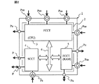
図2には本発明に係る半導体装置のブロック図が例示される。同図に示される半導体装置1は例えばCMOS集積回路製造技術等により単結晶シリコンのような1個の半導体チップに形成された半導体集積回路チップ2を有する。半導体集積回路チップ2は第1回路(FCCT)3,5及び第2回路(SCCT)4を備え、それらはバス6で接続される。第1回路3,5は例えば命令をフェッチして実行する中央処理装置(CPU)及びCPUのワーク領域等に用いられるランダムアクセスメモリ(RAM)を有する。第2回路4はCPUの周辺回路とされ、例えばタイマ(TMR)、シリアル・コミュニケーション・インタフェース(SCI)、ADC(アナログ・ディジタル・コンバータ)、DAC(ディジタル・アナログ・コンバータ)、ウオッチ・ドッグ・タイマ(WDT)、ディジタル・シグナル・プロセッサ(DSP)等の回路を有する。
FIG. 2 illustrates a block diagram of a semiconductor device according to the present invention. The
半導体集積回路チップ2はBGA、LGA又はWPP等の面実装型のパッケージ形態で封止され、そのパッケージには外部端子として代表的に示された外部端子Pus,Pu,Ps,Pが配置される。ここでは第2回路4を使用しない場合を一例とするもので、第1回路3,5は、半導体装置1を搭載して用いる実装基板(図示せず)に接続され、他方の第2回路4は実装基板との接続は必要とされない。前記外部端子Puは半導体装置1を実装する実装基板への接続に用いられスクリーニングテスタとの接続に用いられない端子、前記端子Pusは前記実装基板への接続並びにスクリーニングテスタとの接続に用いられる端子である。前記端子Psは前記実装基板への接続に用いられず且つスクリーニングテスタとの接続に用いられる端子であり、前記端子Pは前記実装基板への接続に用いられず且つスクリーニングテスタとの接続に用いられない端子である。要するに、端子Pus,Puは実装基板に接続される端子、P,Psは実装基板に接続されない端子である。スクリーニングテスタに接続される端子Pus,Psは実装基板に接続される端子と接続されない端子の双方に跨っている。外部端子Pus,Pu,Psのサフィックス“u”は実装基板に接続されることを意味し、サフィックス“s”はスクリーニングテスタに接続されることを意味する。
The semiconductor integrated
図3には半導体装置1を実装基板に搭載した状態が例示される。7は実装基板であり、8は半導体装置1が接続される配線パターンを総称し、前記端子Pus,Puに接続される。
FIG. 3 illustrates a state where the
図4には複数個の半導体装置1がスクリーニングテスタ(TEST)9に接続された状態を例示する。スクリーニングテスタ9に接続された端子Pus,Psは、例えば入力ポート端子I_PORT、クロック入力端子EXTAL、リセット信号入力端子RES、スタンバイ信号入力端子STBY、モード信号入力端子MOD、データ入力端子D0〜D1、電源端子VCC,グランド端子VSSとされる。実装基板7に接続される端子のうちスクリーニングテスタに非接続の端子Puは、例えば入出力ポート端子IO_PORT、出力ポート端子O_PORT、アドレス出力端子A0〜A2とされる。尚、図3、図4における外部端子P,Pus,Ps,Puは作図上半導体装置1の縁辺に沿って図示してあるが、実際にはBGA,LGA,WPPのパッケージ形態の配列になっている。また、端子の数も作図上相違されるが実際には整合されている。
FIG. 4 illustrates a state in which a plurality of
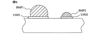
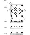
図1には本発明に係る半導体装置の外部端子の配列が例示される。図1の(A)は平面図、(B)〜(G)は正面図である。図1の(A)に例示されるように半導体装置1において、前記端子Pus,Pu,Psは所定ピッチ例えばxy方向に1mmピッチで配置された第1外部端子を構成する。前記端子Pは前記第1外部端子Pus,Pu,Psよりも半導体装置1の中央部寄りに最小ピッチが前記1mmピッチよりも小さなピッチで配置された第2外部端子を構成する。前記第1外部端子Pus,Pu,Psは図5に例示されるように第1ランドLND1に接続された第1バンプBMP1によって形成される。前記第2外部端子Pは前記第1ランドLND1よりも小さな第2ランドLND2に接続され前記第1バンプBMP1よりも高さと径が小さな第2バンプBMP2によって形成される。図1の(B)にはランドLND1,LND2の図示を省略してある。図1の(B)は第1外部端子Pus,Pu,Ps及び第2外部端子Pともにバンプで形成したBGAパッケージ形態の側面断面を概略的に示している。(C)のようにランドを厚く形成した構造(BGA_Pパッケージ形態)、(D)のように第2外部端子Pをランドで形成した構造(BGA/LGAパッケージ形態)を採用する事も可能である。また、図1の(E)のように(D)の形態においてランドを厚く形成した構造(BGA_P/LGA_Pパッケージ形態)、(F)のように第1外部端子Pus,Pu,Ps及び第2外部端子Pともにランドで形成した構造(LGAパッケージ形態)、又は(G)のように(F)の形態においてランドを厚く形成した構造(LGA_Pパッケージ形態)を採用することも可能である。
FIG. 1 illustrates an arrangement of external terminals of a semiconductor device according to the present invention. 1A is a plan view, and FIGS. 1B to 1G are front views. As illustrated in FIG. 1A, in the
図6には図1の外部端子構造に対して第1外部端子Pus,Pu,Ps及び第2外部端子Pの全てを等しいピッチで且つ等しい大きさで形成した場合の比較例が示される。図6の(A)は平面図、(B)〜(G)は正面図である。。図6の(A)〜(G)は図1の(A)〜(G)に対応される。 FIG. 6 shows a comparative example in which all of the first external terminals Pus, Pu, Ps and the second external terminal P are formed with the same pitch and the same size with respect to the external terminal structure of FIG. 6A is a plan view, and FIGS. 6B to 6G are front views. . 6A to 6G correspond to FIGS. 1A to 1G.
上記半導体装置1によれば以下の作用効果を得る。
According to the
〔1〕図1(B)のBGA形態、(C)のBGA_P形態、(D)のBGA/LGA形態、(E)のBGA_p/LGA_P形態においては第2外部端子Pは第1外部端子Pus,Ps,Puに比べ高さと径が小さいから、実装基板7では第2外部端子Pの領域直下に配線パターンがあっても不所望なリークの虞は無い。
[1] In the BGA form of FIG. 1B, the BGA_P form of (C), the BGA / LGA form of (D), and the BGA_p / LGA_P form of (E), the second external terminal P is the first external terminal Pus, Since the height and diameter are smaller than those of Ps and Pu, even if there is a wiring pattern immediately below the region of the second external terminal P on the mounting
〔2〕図1(B)のBGA形態、(C)のBGA_P形態では、第2電極Pがアンダーフィル樹脂で覆われていても、表面を削ることによって容易に露出させることができ、(D)のLGA形態のように第2電極Pをバンプの代わりにランドだけで形成した場合に比べ、不良解析のための端子露出作業が容易になる。要するに、第2電極を覆っているアンダーフィル樹脂の切削代を多く取ることができ、半導体集積回路チップの回路領域を損傷させる虞を未然に回避することができる。 [2] In the BGA form of FIG. 1B and the BGA_P form of FIG. 1C, even if the second electrode P is covered with the underfill resin, it can be easily exposed by scraping the surface. As compared with the case where the second electrode P is formed only by the land instead of the bump as in the LGA form of FIG. In short, it is possible to increase the cutting allowance for the underfill resin covering the second electrode, and to avoid the possibility of damaging the circuit area of the semiconductor integrated circuit chip.
〔3〕実装基板7との接続の可否に拘わらずスクリーニングテスタ9と接続される外部端子Ps,Pusは図1の(B)、(C)、(D)、(E)の形態ではのピッチと径が共に大きなバンプで形成されているのでスクリーニングテスタ9に特別なピンピッチ変換アダプタ等を必要とせず、また、プローブに対するDUTとしての半導体装置1の位置決めについても特に高精度を要しない。これによって、スクリーニングテストのテストコストを低減することが可能になる。図1の(F)、(G)の形態では第2外部端子Pは上記と同じ大きなピッチで配置されているが、ランド若しくはランドを厚くしたポストによって形成されているので、プローブに対するDUTとしての半導体装置1の位置決めについては(B)、(C)、(D)、(E)の形態に比べて高精度を要する。プローブによる半導体集積回路チップの回路領域に対する機械的なダメージを小さくしなければならないからである。スクリーニングテスタに特別なピンピッチ変換アダプタを必要としないことは上記同様である。
[3] The external terminals Ps and Pus connected to the screening tester 9 regardless of whether or not they can be connected to the mounting
〔4〕前記複数の第1外部端子Pus,Ps,Puのうちスクリーニングテスタとの接続に用いられない端子Puは出力端子又は入出力端子であり、出力端子又は入出力端子に接続される回路に対してはその出力機能を利用することにより、内部の回路動作を介して加速試験に適するタイミングや電圧の信号を外部インタフェースバッファまで伝達することが可能である。したがって、スクリーニングのみに利用される端子数を削減することができ、ひいては、大きなピッチで配置すべき大きな外部端子の数が多くなり過ぎるのを抑制することができる。 [4] Of the plurality of first external terminals Pus, Ps, Pu, a terminal Pu that is not used for connection to the screening tester is an output terminal or an input / output terminal, and is a circuit connected to the output terminal or the input / output terminal. On the other hand, by using the output function, it is possible to transmit a timing or voltage signal suitable for the acceleration test to the external interface buffer through the internal circuit operation. Therefore, it is possible to reduce the number of terminals used only for screening, and thus it is possible to suppress an excessive increase in the number of large external terminals that should be arranged with a large pitch.
〔5〕汎用マイクロコンピュータのような半導体装置1の内部回路の一部に特定顧客が使用しない回路がある場合でも当該回路の削減や内部バスからの切り離しを行わないようにすることにより、半導体装置を製造するためのマスクパターンの変更を要しない。このとき、特定顧客が使用しない回路に対してもデバイステストの対象になる。例えば図2のように使用しない回路4はバス6を介して第1の回路3,5に影響を与える場合もあるからである。したがって、図2の外部端子Pのように特定ユーザには使用されない端子は少なくともデバイステストのために配置することが必須であるが、端子ピッチ及び端子サイズを小さくすることによってパッケージの小型化に寄与する。
[5] Even when a part of the internal circuit of the
図7には半導体装置の別の例が示される。図7の(A)は平面図、(B)〜(D)は正面図である。同図に示される半導体装置1Aは、図1で説明した半導体装置1に対し、実装基板への接続に用いられずスクリーニングテスタとの接続に用いられる外部端端子をPPsのように小さく形成した点が相違される。外部端子PPsもその他の第1外部端子Pus,Puと同じピッチで配置されている。即ち、前記外部端子Pus,Puを、第1ランドに接続された第1バンプBMP_Fとによって形成し、前記外部端子PPsを前記第1ランドよりも小さな第2ランドに接続され前記第1バンプよりも高さと径が小さな第2バンプBMP_Sによって形成する。前記外部端子Pを、前記第1ランドよりも小さな第3ランドに接続され前記第1バンプ電極よりも高さと径が小さいた第3バンプBMP_Tによって形成する。その他の構成は図1と同じであるからその詳細な説明は省略する。図7では(A)の平面図の他、(B)のBGA形態、(C)BGA/LGA形態、及び(D)のLGA形態の概略側面断面構造を例示する。これによれば、先に説明した図1の構造に比べて、スクリーニングテストにおいてプローブに対するDUTとしての半導体装置の位置決め高精度を高くすることが必要になる点を除いて上記同様の作用及び効果を得る。
FIG. 7 shows another example of the semiconductor device. FIG. 7A is a plan view, and FIGS. 7B to 7D are front views. The semiconductor device 1A shown in the figure is different from the
図8には第1外部端子Pus,Pu,Ps及び第2外部端子Pの数や配置の異なる別の例が示される。図8の(A)は平面図、(B)〜(D)は正面図である。図1に比べて第1外部端子Pus,Pu,Psのピッチが大きくされ、第2外部端子Pの配列形態が相違される。この配列においての図1と同様の作用効果を得る。 FIG. 8 shows another example in which the number and arrangement of the first external terminals Pus, Pu, Ps and the second external terminals P are different. 8A is a plan view, and FIGS. 8B to 8D are front views. Compared to FIG. 1, the pitch of the first external terminals Pus, Pu, Ps is increased, and the arrangement form of the second external terminals P is different. In this arrangement, the same effect as in FIG. 1 is obtained.
図9には図8の端子配列に対し、スクリーニングテスタとの接続のみに用いられる外部端端子をPPsのように第3バンプBMP_Tにより小さく形成した構成が例示される。図9の(A)は平面図、(B)〜(D)は正面図である。外部端子PPsもその他の第1外部端子Pus,Psと同じピッチで配置されている。この構成においても図7と上記同様の作用及び効果を得る。 FIG. 9 illustrates a configuration in which external terminal terminals used only for connection with the screening tester are formed smaller by third bumps BMP_T, such as PPs, with respect to the terminal arrangement of FIG. 9A is a plan view, and FIGS. 9B to 9D are front views. The external terminals PPs are also arranged at the same pitch as the other first external terminals Pus and Ps. Even in this configuration, the same operations and effects as in FIG. 7 are obtained.
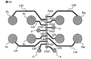
図10にはWPPパッケージ形態における端子配列が例示される。WPPパッケージ形態では半導体集積回路チップのボンディングパッド形成領域PADの上にボンディングパッドPADに接続して延在する引き出し配線LINが形成され、前記第1外部端子Pus,Pu,Ps及び第2外部端子Pは対応する引き出し配線LINの先端部に例えば半田バンプ電極によって形成される。WPPパッケージ形態においても図1の場合と同様の作用効果を得る。 FIG. 10 illustrates a terminal arrangement in the WPP package form. In the WPP package form, a lead-out wiring LIN extending to connect to the bonding pad PAD is formed on the bonding pad forming region PAD of the semiconductor integrated circuit chip, and the first external terminals Pus, Pu, Ps and the second external terminal P are formed. Are formed by, for example, solder bump electrodes at the tip of the corresponding lead-out wiring LIN. Also in the WPP package form, the same effect as in the case of FIG. 1 is obtained.
以上本発明者によってなされた発明を実施形態に基づいて具体的に説明したが、本発明はそれに限定されるものではなく、その要旨を逸脱しない範囲において種々変更可能であることは言うまでもない。 Although the invention made by the present inventor has been specifically described based on the embodiments, it is needless to say that the present invention is not limited thereto and can be variously modified without departing from the gist thereof.
例えば、バンプの形状は球形に限定されず、立方体形状、逆三角錐台形状、逆円錐台形状等であってもよい。外部端子の数、一つのパッケージに納められる半導体集積回路チップの数、第1回路及び第2回路の具体的な種類や数等については適宜変更可能である。 For example, the shape of the bump is not limited to a spherical shape, and may be a cubic shape, an inverted triangular truncated cone shape, an inverted truncated truncated cone shape, or the like. The number of external terminals, the number of semiconductor integrated circuit chips contained in one package, the specific types and numbers of the first circuit and the second circuit, and the like can be changed as appropriate.
また、本発明の実施の形態では、配線基板の周囲に配置され(各辺に沿って配置され)、第1バンプが接続される第1ランドの径が、第2バンプが接続される第2ランドの径よりも小さく形成されていることについて説明したが、これに限定されるものではなく、例えば図11に示すように、半導体装置を実装する実装基板の電極とは接続されないが、スクリーニングテスタとの接続に使用される第2ランドには、第1バンプの高さよりも低い第2バンプが形成されていればよく、第2ランドの径は第1ランドの径と同じ寸法であってもよい。これは、スクリーニングテストが、プローブ針をバンプに接触させて行うが、このときランドの径が相対的に大きいほうが確実にプローブ針をバンプに接触させ易いためである。しかしながら、単にランドを大きくしてしまうと、形成されるバンプの高さも高くなってしまう。スクリーニングテストに使用されるバンプは、半導体装置を実装する実装基板の電極には接続しないため、バンプの高さはできるだけ低く形成しておきたい。そこで、図11(図11(B)は図11(A)におけるA-A'線の断面図、図11(C)は図11(A)におけるB-B'線の断面図、図11(D)は図11(A)におけるC-C'線の断面図)に示すような構成とすれば、実装基板との接触を避けながら、スクリーニングテストをより確実に行うことができる。 In the embodiment of the present invention, the diameter of the first land arranged around the wiring substrate (arranged along each side) to which the first bump is connected is set to be the second value to which the second bump is connected. Although it has been described that it is smaller than the diameter of the land, the present invention is not limited to this. For example, as shown in FIG. 11, it is not connected to the electrode of the mounting substrate on which the semiconductor device is mounted. As long as the second land used for connection to the second land has a second bump lower than the height of the first bump, the second land has the same diameter as the first land. Good. This is because the screening test is performed by bringing the probe needle into contact with the bump, and at this time, the probe needle is surely brought into contact with the bump when the land diameter is relatively large. However, if the land is simply increased, the height of the bump formed is also increased. The bump used for the screening test is not connected to the electrode of the mounting substrate on which the semiconductor device is mounted. Therefore, the bump height should be as low as possible. Therefore, FIG. 11 (FIG. 11B is a cross-sectional view taken along the line AA ′ in FIG. 11A, FIG. 11C is a cross-sectional view taken along the line BB ′ in FIG. 11A, and FIG. If D) is configured as shown in the cross-sectional view taken along the line CC ′ in FIG. 11A, the screening test can be performed more reliably while avoiding contact with the mounting substrate.
また、本発明の実施の形態におけるWPPパッケージでは、半導体チップ(半導体集積回路チップ)のボンディングパッドから引き出し配線を介して隣接するボンディングパッド同士の間隔を広げ、引き出し配線の先端部に半田バンプを形成することについて説明したが、これに限定されるものではなく、例えば半導体チップに形成される複数のボンディングパッド同士の間隔が予め広く配置されていれば、引き出し配線を各ボンディングパッドから延在させる必要はない。しかしながら、半導体チップに形成されるボンディングパッドの寸法(面積、径)は、配線基板に形成されるランドに比べると相対的に小さいため、これらのボンディングパッドに直接半田バンプを形成した場合、形成される半田バンプも小さく(低く)なってしまう。そこで、図12に示すように、ボンディングパッド上に第1絶縁膜および第2絶縁膜を介して引き出し配線を形成し、半田バンプが接続される領域を広げることで、形成される半田バンプを相対的に大きく(高く)することができ、WPPパッケージ(半導体装置、半導体チップ、半導体集積回路チップ)の実装強度を向上することができる。
また、本発明の実施の形態では、BGA型またはLGA型のパッケージについても説明したが、樹脂封止体(封止体)で覆われている半導体チップ(半導体集積回路チップ)と、半導体チップを支持(搭載)する配線基板との電気的な接続は、図13に示すように、複数のワイヤを用いても良く、さらには図14に示すように、バンプ電極を介してフリップチップ接続しても良い。
Further, in the WPP package according to the embodiment of the present invention, the distance between adjacent bonding pads is extended from the bonding pad of the semiconductor chip (semiconductor integrated circuit chip) via the lead wiring, and a solder bump is formed at the leading end of the lead wiring. However, the present invention is not limited to this. For example, if a plurality of bonding pads formed on a semiconductor chip are spaced widely in advance, it is necessary to extend the lead-out wiring from each bonding pad. There is no. However, since the dimensions (area and diameter) of the bonding pads formed on the semiconductor chip are relatively small compared to the lands formed on the wiring substrate, the bonding pads are formed when the solder bumps are formed directly on these bonding pads. Solder bumps that are smaller are also smaller (lower). Therefore, as shown in FIG. 12, a lead-out wiring is formed on the bonding pad via the first insulating film and the second insulating film, and the area to which the solder bump is connected is widened so that the formed solder bump is relatively The mounting strength of the WPP package (semiconductor device, semiconductor chip, semiconductor integrated circuit chip) can be improved.
In the embodiment of the present invention, a BGA type or LGA type package is also described. However, a semiconductor chip (semiconductor integrated circuit chip) covered with a resin sealing body (sealing body) and a semiconductor chip are provided. As shown in FIG. 13, a plurality of wires may be used for electrical connection with the wiring board to be supported (mounted). Further, as shown in FIG. 14, flip-chip connection is performed via bump electrodes. Also good.
1 半導体装置
2 半導体集積回路チップ
3,5 第1回路(FCCT)
4 第2回路(SCCT)
6 バス
Pu 実装基板への接続に用いられスクリーニングテスタとの接続に用いられない端子
Pus 前記実装基板への接続並びにスクリーニングテスタとの接続に用いられる端子
Ps 前記実装基板への接続に用いられず且つスクリーニングテスタとの接続に用いられる端子
P 前記実装基板への接続に用いられず且つスクリーニングテスタとの接続に用いられない端子
7 実装基板
8 配線パターン
9 スクリーニングテスタ(TEST)
LND1 第1ランド
BMP1 第1バンプ
LND2 第2ランド
BMP2 第2バンプ
BMP_F 第1バンプ
BMP_S 第2バンプ
BMP_T 第3バンプ
PAD ボンディングパッド形成領域
LIN 引き出し配線
DESCRIPTION OF
4 Second circuit (SCCT)
6 Bus Pu Terminal used for connection to mounting board and not used for connection to screening tester Pus Terminal used for connection to mounting board and connection to screening tester Ps Not used for connection to mounting board and Terminal P used for connection to screening tester P Terminal not used for connection to mounting board and not used for connection to
LND1 First land BMP1 First bump LND2 Second land BMP2 Second bump BMP_F First bump BMP_S Second bump BMP_T Third bump PAD Bonding pad formation area LIN Lead wiring
Claims (5)
(a)第1の面と、前記第1の面に形成され、且つ第1ピッチで配置された複数の第1ランドと、前記第1の面に形成され、且つ前記複数の第1ランドよりも小さく形成され、且つ前記複数の第1ランドよりも前記第1の面の中央部寄りに前記第1ピッチよりも小さな第2ピッチで配置された複数の第2ランドと、前記複数の第1ランドにそれぞれ接続され、且つ第1の高さを有し、且つ第1の径を有する複数の第1バンプと、前記複数の第2ランドにそれぞれ接続され、且つ前記第1の高さよりも小さな第2の高さを有し、且つ前記第1の径よりも小さな第2の径を有する複数の第2バンプと、を備えた半導体装置を準備する工程;
(b)前記複数の第1バンプを介して前記半導体装置を実装基板に実装し、前記複数の第1バンプおよび前記複数の第2バンプをアンダーフィル樹脂で覆う工程、
ここで、
前記半導体装置は、さらに、回路が形成された半導体集積回路チップを備えており、
前記回路として、第1回路と前記第1回路に信号線によって接続される第2回路とを有し、
前記第2回路に接続される外部端子の一部又は全部は、前記第2バンプであり、
前記第1回路に接続される外部端子の全部は、前記第1バンプである。 A semiconductor device mounting method including the following steps:
(A) a first surface, a plurality of first lands formed on the first surface and arranged at a first pitch, and formed on the first surface and from the plurality of first lands And a plurality of second lands disposed at a second pitch smaller than the first pitch closer to the center of the first surface than the plurality of first lands, and the plurality of first lands. A plurality of first bumps connected to the lands, having a first height and having a first diameter, and connected to the plurality of second lands, respectively, and being smaller than the first height Providing a semiconductor device including a plurality of second bumps having a second height and a second diameter smaller than the first diameter;
(B) mounting the semiconductor device on a mounting substrate via the plurality of first bumps, and covering the plurality of first bumps and the plurality of second bumps with an underfill resin ;
here,
The semiconductor device further includes a semiconductor integrated circuit chip on which a circuit is formed,
The circuit includes a first circuit and a second circuit connected to the first circuit by a signal line,
A part or all of the external terminals connected to the second circuit are the second bumps,
All of the external terminals connected to the first circuit are the first bumps.
前記複数の第1バンプは、前記実装基板への接続に用いられる端子、前記実装基板への接続並びにスクリーニングテスタとの接続に用いられる端子、及び前記実装基板への接続に用いられず、且つスクリーニングテスタとの接続に用いられる端子に割り当てられ、
前記複数の第2バンプは、前記実装基板への接続に用いられず且つスクリーニングテスタとの接続に用いられない端子に割り当てられる。 The method for mounting a semiconductor device according to claim 1,
The plurality of first bumps are not used for connection to the mounting substrate, a terminal used for connection to the mounting substrate and a connection to a screening tester, and a connection to the mounting substrate, and screening. Assigned to the terminal used to connect to the tester,
The plurality of second bumps are assigned to terminals that are not used for connection to the mounting substrate and are not used for connection to the screening tester.
前記複数の第2バンプのうちスクリーニングテスタとの接続に用いられない端子は出力端子又は入出力端子である。 In the mounting method of the semiconductor device according to claim 2,
Of the plurality of second bumps, a terminal that is not used for connection with the screening tester is an output terminal or an input / output terminal.
前記複数の第1バンプのうちスクリーニングテスタとの接続に用いられる端子は入力端子である。 In the mounting method of the semiconductor device according to claim 3,
Of the plurality of first bumps, a terminal used for connection to the screening tester is an input terminal.
前記第1回路は、命令を実行する中央処理装置を含み、
前記第2回路は、前記中央処理装置によって制御される周辺回路を含む。 The method for mounting a semiconductor device according to claim 1,
The first circuit includes a central processing unit that executes instructions;
The second circuit includes a peripheral circuit controlled by the central processing unit.
Priority Applications (1)
| Application Number | Priority Date | Filing Date | Title |
|---|---|---|---|
| JP2007213554A JP5144170B2 (en) | 2007-08-20 | 2007-08-20 | Mounting method of semiconductor device |
Applications Claiming Priority (1)
| Application Number | Priority Date | Filing Date | Title |
|---|---|---|---|
| JP2007213554A JP5144170B2 (en) | 2007-08-20 | 2007-08-20 | Mounting method of semiconductor device |
Publications (3)
| Publication Number | Publication Date |
|---|---|
| JP2009049170A JP2009049170A (en) | 2009-03-05 |
| JP2009049170A5 JP2009049170A5 (en) | 2010-09-30 |
| JP5144170B2 true JP5144170B2 (en) | 2013-02-13 |
Family
ID=40501128
Family Applications (1)
| Application Number | Title | Priority Date | Filing Date |
|---|---|---|---|
| JP2007213554A Expired - Fee Related JP5144170B2 (en) | 2007-08-20 | 2007-08-20 | Mounting method of semiconductor device |
Country Status (1)
| Country | Link |
|---|---|
| JP (1) | JP5144170B2 (en) |
Families Citing this family (3)
| Publication number | Priority date | Publication date | Assignee | Title |
|---|---|---|---|---|
| JP5342422B2 (en) | 2009-12-10 | 2013-11-13 | ルネサスエレクトロニクス株式会社 | Semiconductor device and manufacturing method thereof |
| CN110473839A (en) | 2018-05-11 | 2019-11-19 | 三星电子株式会社 | Semiconductor packaging system |
| US10991638B2 (en) | 2018-05-14 | 2021-04-27 | Samsung Electronics Co., Ltd. | Semiconductor package system |
Family Cites Families (6)
| Publication number | Priority date | Publication date | Assignee | Title |
|---|---|---|---|---|
| JPS63271966A (en) * | 1987-04-28 | 1988-11-09 | Nec Corp | Semiconductor integrated circuit |
| JPH03172782A (en) * | 1989-12-01 | 1991-07-26 | Hitachi Ltd | Semiconductor integrated circuit |
| JP4509437B2 (en) * | 2000-09-11 | 2010-07-21 | Hoya株式会社 | Manufacturing method of multilayer wiring board |
| JP2004335858A (en) * | 2003-05-09 | 2004-11-25 | Murata Mfg Co Ltd | Electronic device and electronic apparatus employing the same |
| JP2004078996A (en) * | 2003-11-17 | 2004-03-11 | Renesas Technology Corp | Data processor |
| JP2007115904A (en) * | 2005-10-20 | 2007-05-10 | Renesas Technology Corp | Method of manufacturing semiconductor device |
-
2007
- 2007-08-20 JP JP2007213554A patent/JP5144170B2/en not_active Expired - Fee Related
Also Published As
| Publication number | Publication date |
|---|---|
| JP2009049170A (en) | 2009-03-05 |
Similar Documents
| Publication | Publication Date | Title |
|---|---|---|
| JP5165404B2 (en) | Semiconductor device, semiconductor device manufacturing method and test method | |
| US8202740B2 (en) | Method of manufacturing a semiconductor device and a testing method of the same | |
| TWI447408B (en) | Test interposer having active circuit component and method therefor | |
| JP2005209239A (en) | Semiconductor integrated circuit apparatus | |
| US7476555B2 (en) | Method of chip manufacturing | |
| US8395404B2 (en) | Electronic device including electronic part and wiring substrate | |
| JP2010278471A (en) | Semiconductor device, and module | |
| US20040017216A1 (en) | Multi-socket board for open/short tester | |
| JP5144170B2 (en) | Mounting method of semiconductor device | |
| US7868439B2 (en) | Chip package and substrate thereof | |
| JP4539396B2 (en) | Mounting structure of semiconductor device | |
| JP2006351664A (en) | Semiconductor device | |
| JP2016514367A (en) | Package substrate with test pads on fine pitch trace | |
| JP2004022664A (en) | Packaging and testing circuit of semiconductor device | |
| US20210274641A1 (en) | Semiconductor apparatus | |
| US20210274643A1 (en) | Semiconductor apparatus | |
| US20060097285A1 (en) | Microcomputer chip with function capable of supporting emulation | |
| JP4022698B2 (en) | Inspection circuit board | |
| JP2004311535A (en) | Chip-size package semiconductor device | |
| JP7400536B2 (en) | semiconductor equipment | |
| JP2002007164A (en) | Chip for semiconductor integrated circuit and emulation system | |
| JP4627306B2 (en) | Semiconductor device | |
| JP2015115567A (en) | Electronic device | |
| JP2010062469A (en) | Semiconductor module | |
| US20030183908A1 (en) | Semiconductor device and method of manufacturing the same |
Legal Events
| Date | Code | Title | Description |
|---|---|---|---|
| A711 | Notification of change in applicant |
Free format text: JAPANESE INTERMEDIATE CODE: A712 Effective date: 20100507 |
|
| A521 | Written amendment |
Free format text: JAPANESE INTERMEDIATE CODE: A523 Effective date: 20100816 |
|
| A621 | Written request for application examination |
Free format text: JAPANESE INTERMEDIATE CODE: A621 Effective date: 20100816 |
|
| A977 | Report on retrieval |
Free format text: JAPANESE INTERMEDIATE CODE: A971007 Effective date: 20120131 |
|
| A131 | Notification of reasons for refusal |
Free format text: JAPANESE INTERMEDIATE CODE: A131 Effective date: 20120209 |
|
| A521 | Written amendment |
Free format text: JAPANESE INTERMEDIATE CODE: A523 Effective date: 20120329 |
|
| TRDD | Decision of grant or rejection written | ||
| A01 | Written decision to grant a patent or to grant a registration (utility model) |
Free format text: JAPANESE INTERMEDIATE CODE: A01 Effective date: 20121115 |
|
| A01 | Written decision to grant a patent or to grant a registration (utility model) |
Free format text: JAPANESE INTERMEDIATE CODE: A01 |
|
| A61 | First payment of annual fees (during grant procedure) |
Free format text: JAPANESE INTERMEDIATE CODE: A61 Effective date: 20121122 |
|
| FPAY | Renewal fee payment (event date is renewal date of database) |
Free format text: PAYMENT UNTIL: 20151130 Year of fee payment: 3 |
|
| R150 | Certificate of patent or registration of utility model |
Free format text: JAPANESE INTERMEDIATE CODE: R150 |
|
| S531 | Written request for registration of change of domicile |
Free format text: JAPANESE INTERMEDIATE CODE: R313531 |
|
| R350 | Written notification of registration of transfer |
Free format text: JAPANESE INTERMEDIATE CODE: R350 |
|
| LAPS | Cancellation because of no payment of annual fees |