WO2009101911A1 - 半導体レーザ素子 - Google Patents
半導体レーザ素子 Download PDFInfo
- Publication number
- WO2009101911A1 WO2009101911A1 PCT/JP2009/052128 JP2009052128W WO2009101911A1 WO 2009101911 A1 WO2009101911 A1 WO 2009101911A1 JP 2009052128 W JP2009052128 W JP 2009052128W WO 2009101911 A1 WO2009101911 A1 WO 2009101911A1
- Authority
- WO
- WIPO (PCT)
- Prior art keywords
- film
- thickness
- nitride
- layer
- semiconductor laser
- Prior art date
- Legal status (The legal status is an assumption and is not a legal conclusion. Google has not performed a legal analysis and makes no representation as to the accuracy of the status listed.)
- Ceased
Links
Images

Classifications
-
- H—ELECTRICITY
- H01—ELECTRIC ELEMENTS
- H01S—DEVICES USING THE PROCESS OF LIGHT AMPLIFICATION BY STIMULATED EMISSION OF RADIATION [LASER] TO AMPLIFY OR GENERATE LIGHT; DEVICES USING STIMULATED EMISSION OF ELECTROMAGNETIC RADIATION IN WAVE RANGES OTHER THAN OPTICAL
- H01S5/00—Semiconductor lasers
- H01S5/30—Structure or shape of the active region; Materials used for the active region
- H01S5/34—Structure or shape of the active region; Materials used for the active region comprising quantum well or superlattice structures, e.g. single quantum well [SQW] lasers, multiple quantum well [MQW] lasers or graded index separate confinement heterostructure [GRINSCH] lasers
- H01S5/343—Structure or shape of the active region; Materials used for the active region comprising quantum well or superlattice structures, e.g. single quantum well [SQW] lasers, multiple quantum well [MQW] lasers or graded index separate confinement heterostructure [GRINSCH] lasers in AIIIBV compounds, e.g. AlGaAs-laser, InP-based laser
- H01S5/34333—Structure or shape of the active region; Materials used for the active region comprising quantum well or superlattice structures, e.g. single quantum well [SQW] lasers, multiple quantum well [MQW] lasers or graded index separate confinement heterostructure [GRINSCH] lasers in AIIIBV compounds, e.g. AlGaAs-laser, InP-based laser with a well layer based on Ga(In)N or Ga(In)P, e.g. blue laser
-
- B—PERFORMING OPERATIONS; TRANSPORTING
- B82—NANOTECHNOLOGY
- B82Y—SPECIFIC USES OR APPLICATIONS OF NANOSTRUCTURES; MEASUREMENT OR ANALYSIS OF NANOSTRUCTURES; MANUFACTURE OR TREATMENT OF NANOSTRUCTURES
- B82Y20/00—Nanooptics, e.g. quantum optics or photonic crystals
-
- H—ELECTRICITY
- H01—ELECTRIC ELEMENTS
- H01S—DEVICES USING THE PROCESS OF LIGHT AMPLIFICATION BY STIMULATED EMISSION OF RADIATION [LASER] TO AMPLIFY OR GENERATE LIGHT; DEVICES USING STIMULATED EMISSION OF ELECTROMAGNETIC RADIATION IN WAVE RANGES OTHER THAN OPTICAL
- H01S5/00—Semiconductor lasers
- H01S5/02—Structural details or components not essential to laser action
- H01S5/028—Coatings ; Treatment of the laser facets, e.g. etching, passivation layers or reflecting layers
- H01S5/0287—Facet reflectivity
-
- H—ELECTRICITY
- H01—ELECTRIC ELEMENTS
- H01S—DEVICES USING THE PROCESS OF LIGHT AMPLIFICATION BY STIMULATED EMISSION OF RADIATION [LASER] TO AMPLIFY OR GENERATE LIGHT; DEVICES USING STIMULATED EMISSION OF ELECTROMAGNETIC RADIATION IN WAVE RANGES OTHER THAN OPTICAL
- H01S5/00—Semiconductor lasers
- H01S5/20—Structure or shape of the semiconductor body to guide the optical wave ; Confining structures perpendicular to the optical axis, e.g. index or gain guiding, stripe geometry, broad area lasers, gain tailoring, transverse or lateral reflectors, special cladding structures, MQW barrier reflection layers
- H01S5/2004—Confining in the direction perpendicular to the layer structure
- H01S5/2009—Confining in the direction perpendicular to the layer structure by using electron barrier layers
-
- H—ELECTRICITY
- H01—ELECTRIC ELEMENTS
- H01S—DEVICES USING THE PROCESS OF LIGHT AMPLIFICATION BY STIMULATED EMISSION OF RADIATION [LASER] TO AMPLIFY OR GENERATE LIGHT; DEVICES USING STIMULATED EMISSION OF ELECTROMAGNETIC RADIATION IN WAVE RANGES OTHER THAN OPTICAL
- H01S5/00—Semiconductor lasers
- H01S5/20—Structure or shape of the semiconductor body to guide the optical wave ; Confining structures perpendicular to the optical axis, e.g. index or gain guiding, stripe geometry, broad area lasers, gain tailoring, transverse or lateral reflectors, special cladding structures, MQW barrier reflection layers
- H01S5/22—Structure or shape of the semiconductor body to guide the optical wave ; Confining structures perpendicular to the optical axis, e.g. index or gain guiding, stripe geometry, broad area lasers, gain tailoring, transverse or lateral reflectors, special cladding structures, MQW barrier reflection layers having a ridge or stripe structure
-
- H—ELECTRICITY
- H01—ELECTRIC ELEMENTS
- H01S—DEVICES USING THE PROCESS OF LIGHT AMPLIFICATION BY STIMULATED EMISSION OF RADIATION [LASER] TO AMPLIFY OR GENERATE LIGHT; DEVICES USING STIMULATED EMISSION OF ELECTROMAGNETIC RADIATION IN WAVE RANGES OTHER THAN OPTICAL
- H01S5/00—Semiconductor lasers
- H01S5/30—Structure or shape of the active region; Materials used for the active region
- H01S5/305—Structure or shape of the active region; Materials used for the active region characterised by the doping materials used in the laser structure
- H01S5/3054—Structure or shape of the active region; Materials used for the active region characterised by the doping materials used in the laser structure p-doping
- H01S5/3063—Structure or shape of the active region; Materials used for the active region characterised by the doping materials used in the laser structure p-doping using Mg
Definitions
- the present invention relates to a semiconductor laser element, and more particularly, to a semiconductor laser element including a semiconductor element layer having a light emitting layer.
- semiconductor lasers are widely used as light sources for optical disk systems and optical communication systems.
- improvements in the performance of equipment constituting the system there is a demand for improvement in the characteristics of semiconductor lasers as component parts.
- semiconductor lasers as light sources for high-density optical disk systems, it is desired to shorten the wavelength and output of laser light.
- blue-violet semiconductor lasers having an oscillation wavelength of about 405 nm have been developed using nitride materials. Higher output is being studied.
- an end surface coating process is performed in the manufacturing process to make the light emitting surface of the resonator of the semiconductor laser element have a low reflectance and to make the light reflecting surface have a high reflectance. Is done.
- a dielectric film made of an oxide film such as SiO 2 or Al 2 O 3 has been conventionally used for end face coating of a resonator.
- oxygen in the dielectric film diffuses into the semiconductor layer, causing the semiconductor layer to be oxidized, and a non-radiative recombination level at the interface between the semiconductor layer and the end face coat film. (A state where light emission energy is converted into heat energy) occurs.
- the laser light is easily absorbed by the semiconductor layer and the end face coat film, and there is a disadvantage that optical damage destruction (COD) occurs due to abnormal heat generation at the end face of the resonator.
- COD optical damage destruction
- an end surface coating process using a dielectric film made of a nitride film not containing oxygen has been proposed.
- the stress of a nitride film is several to several tens of times greater than that of an oxide film, so that film peeling (peeling) is likely to occur.
- peeling film peeling
- a first coat film made of an oxide is formed on the light emitting side resonator end face, and between the light emitting side resonator end face and the first coat film.
- a nitride semiconductor light emitting device in which a second coat film made of nitride is formed so as to be sandwiched is disclosed.
- a second coat film made of nitride is formed so as to be sandwiched.
- the first coat film on the outermost surface exposed to the atmosphere by the second coat film made of nitride formed so as to be in contact with the resonator end face Oxygen is suppressed from being supplied to the semiconductor layer (resonator end face on the light emission side).
- a high energy laser beam having a wavelength of about 400 nm and a high light density is emitted from the end face of the resonator.
- Heat is generated in the first coat film and the second coat film.
- oxygen is desorbed from the first coat film made of oxide by heat generation at the interface between the first coat film and the second coat film.
- the reaction rate at which oxygen is desorbed from the first coat film made of an oxide is higher than the reaction rate of substitution between nitrogen and oxygen in the second coat film. For this reason, the first coat film gradually begins to deteriorate as the laser beam is emitted. As a result, the operating current of the laser element is increased, and the end face of the resonator is easily destroyed due to further heat generation accompanying the increase of the operating current. In particular, in a semiconductor laser with high output, the above points become more prominent as the laser operating time is longer, and there is a problem that the reliability of the laser element is lowered.
- the present invention has been made to solve the above-described problems, and one object of the present invention is to provide a semiconductor laser device capable of improving the reliability of the laser device.
- a semiconductor laser device includes a semiconductor element layer having a light emitting layer, a first resonator end face formed at an end of a light emitting side of a region including the light emitting layer of the semiconductor element layer, A first nitride film, a first intermediate film including at least one of the first oxide film and the first oxynitride film, and a second nitride film are formed in this order on the resonator end face from the first resonator end face side.
- a first insulating film and a second insulating film formed on the first insulating film and including at least one of the second oxide film and the second oxynitride film, and the wavelength of the laser light emitted from the light emitting layer is ⁇
- the refractive index of the first nitride film, the average refractive index of the first intermediate film, and the refractive index of the second nitride film are n1, n2, and n3, respectively
- the thickness t1 of the first nitride film, the first The thickness t2 of the intermediate film and the thickness t3 of the second nitride film are t1 ⁇ / (4 ⁇ n1), respectively.
- t2 ⁇ / (4 ⁇ n2) and t3 ⁇ is set to be ⁇ / (4 ⁇ n3).
- the cavity facets on the light emission side are distinguished by the magnitude relationship of the intensity of the laser light emitted from each of the pair of cavity facets formed. That is, the side where the laser beam emission intensity is relatively large is the first resonator end face on the light emission side. Further, the side where the laser beam emission intensity is relatively small is the second resonator end face on the light reflection side.
- the first nitride film, the first oxide film, and the first acid are formed on the first resonator end face on the light emission side from the first resonator end face side.
- a first insulating film including a first intermediate film including at least one of the nitride films and a second nitride film in this order is provided.
- the second nitride film disposed on the outside makes it difficult for oxygen present in the second insulating film and the atmosphere to be taken into the first insulating film, so that the first intermediate film and the first nitride film Oxygen detachment at the interface and substitution reaction between oxygen and nitrogen are suppressed.
- the interface between the first intermediate film and the first nitride film is prevented from being altered and deteriorated. Further, even when alteration occurs at the interface between the first intermediate film and the first nitride film, the altered region extending in the first intermediate film can be retained in this region by the first nitride film and the second nitride film. As a result, expansion of alteration is suppressed. Thereby, alteration in the first insulating film can be minimized. Therefore, even when the output power of the laser emission light is increased, the heat generation near the first resonator end face and the first insulating film on the light emission side is suppressed, so that the destruction of the first resonator end face is suppressed. As a result, the reliability of the laser element can be improved.
- the second insulating film includes at least one of a second oxide film and a second oxynitride film formed on the first insulating film, that is, on the surface of the first insulating film located on the opposite side of the first resonator end face.
- the thickness t1, the thickness t2 of the first intermediate film, and the thickness t3 of the second nitride film constituting the first insulating film are t1 ⁇ / (4 ⁇ n1) and t2 ⁇ /, respectively.
- the thickness of each film constituting the first insulating film becomes smaller than ⁇ / (4 ⁇ n).
- the influence of the first insulating film on the reflectance control function of the second insulating film set to have a desired reflectance can be easily suppressed.
- the thickness of each film constituting the first insulating film is thin, film peeling (peeling) due to stress after film formation can be suppressed.
- the first nitride film is preferably in contact with the semiconductor device layer. According to this structure, since the first nitride film is in contact with the first resonator end face on the light emitting side, the first oxide film and the first oxynitride film in the first intermediate film are separated from at least one of them. Incorporation of oxygen into the semiconductor element layer can be easily suppressed by the first nitride film.
- At least one of the first nitride film and the second nitride film and the first intermediate film contain the same metal element.
- at least one of the first nitride film and the first intermediate film that are in contact with each other and the second nitride film and the first intermediate film that are in contact with each other is a material containing the same type of metal element, Adhesion at the time of contact can be improved. As a result, peeling (peeling) of at least one of the first nitride film and the second nitride film can be suppressed.
- the first nitride film and the second nitride film each include at least one of Al and Si.
- the nitride containing at least one of Al and Si has good insulation, the insulation of the first nitride film and the second nitride film can be improved.
- the nitride film containing at least one of Al and Si can effectively suppress oxygen from being taken into the first insulating film and the semiconductor element layer.
- the first oxide film preferably contains at least one element selected from the group consisting of Al, Si, Zr, Ta, Hf, and Nb. If comprised in this way, since the oxide containing said element has favorable insulation, the insulation of a 1st oxide film can be improved.
- the first oxide film and the first nitride film and the second nitride film sandwiching the first oxide film from both sides contain a common element selected from the above group, the first oxide film, The adhesion between the first nitride film and the second nitride film can be improved.
- the first oxynitride film preferably contains at least one of Al and Si. If comprised in this way, since the oxide containing at least one of Al and Si has favorable insulation, the insulation of a 1st oxynitride film can be improved. Further, when the first oxynitride film containing Al element is sandwiched from both sides by the first nitride film and second nitride film containing Al element, each film is easily brought into contact with the same kind of metal element (Al element). Therefore, the adhesion between the films can be improved.
- Al element metal element
- a second intermediate film including at least one of a third oxide film and a third oxynitride film is further formed between the first insulating film and the second insulating film.
- the average refractive index of the second intermediate film is n4 and the thickness is t4, t4 ⁇ / (4 ⁇ n4) is set.
- the thickness of the second intermediate film is smaller than ⁇ / (4 ⁇ n)
- the laser light emitted from the first resonator end face on the light emission side has the thickness of the second intermediate film. It penetrates without being affected and reaches the second insulating film. Thereby, it is possible to easily suppress the reflectance control function of the second insulating film set to have a desired reflectance from being influenced by the second intermediate film.
- the first intermediate film preferably includes both a first oxide film and a first oxynitride film. That is, both the first oxide film and the first oxynitride film are formed between the first nitride film and the second nitride film.
- oxygen present in the second insulating film and in the atmosphere is more difficult to be taken into the first insulating film, so that the interface between the first intermediate film and the first nitride film is altered and deteriorated. This can be further suppressed.
- the first intermediate film preferably includes the first oxide film and two first acids sandwiching the first oxide film in the stacking direction. It consists of a nitride film.
- the first insulating film is laminated in the order of the nitride film, the oxynitride film, the oxide film, the oxynitride film, and the nitride film, so that the composition in the first insulating film gradually changes. .
- the adhesiveness between the respective films in the first insulating film can be further improved, so that the strength of the first insulating film composed of a plurality of thin films can be maintained.
- the second resonator end face formed on the light reflection side end portion of the region including the light emitting layer of the semiconductor element layer, and the second resonator end face be formed on the second resonator end face.
- the refractive index of the third nitride film, the average refractive index of the third intermediate film, and the refractive index of the fourth nitride film are n5, n6, and n7, respectively.
- the thickness t5 of the third nitride film, the thickness t6 of the third intermediate film, and the thickness t7 of the fourth nitride film are t5 ⁇ / (4 ⁇ n5), t6 ⁇ / (4 ⁇ n6) and t7, respectively. It is set so that ⁇ / (4 ⁇ n7).
- a reflection film that reflects laser light on the third insulating film that is, on the surface of the third insulating film that is located on the opposite side of the second resonator end surface on the light reflecting side.
- the thickness of each film constituting the third insulating film is smaller than ⁇ / (4 ⁇ n).
- the laser light emitted from the end face of the second resonator on the light reflecting side is transmitted regardless of the thickness of each film constituting the third insulating film and reaches the reflecting film. It is possible to easily suppress the reflectance control function of the reflective film set to have the influence of the third insulating film.
- the thickness of each film constituting the third insulating film is thin, film peeling (peeling) due to stress after film formation can be suppressed.
- the third nitride film is in contact with the semiconductor element layer. If comprised in this way, since the 3rd nitride film is contacting the 2nd resonator end surface by the side of light reflection, it will come from at least one of the 4th oxide film and the 4th oxynitride film in the 3rd intermediate film Incorporation of oxygen into the semiconductor element layer can be easily suppressed by the third nitride film.
- At least one of the third nitride film and the fourth nitride film and the third intermediate film contain the same metal element.
- at least one of the third nitride film and the third intermediate film that are in contact with each other and the fourth nitride film and the third intermediate film that are in contact with each other is a material containing the same type of metal element. Adhesion at the time of contact can be improved. As a result, peeling (peeling) of at least one of the third nitride film and the fourth nitride film can be suppressed.
- the third nitride film and the fourth nitride film each include at least one of Al and Si.
- the insulation of the third nitride film and the fourth nitride film can be improved.
- the nitride film containing at least one of Al and Si can effectively suppress oxygen from being taken into the third insulating film and the semiconductor element layer.
- the fourth oxide film contains at least one element selected from the group consisting of Al, Si, Zr, Ta, Hf, and Nb. If comprised in this way, since the oxide containing said element has favorable insulation, the insulation of a 4th oxide film can be improved.
- the fourth oxide film and the third nitride film and the fourth nitride film sandwiching the fourth oxide film from both sides contain a common element selected from the group, the fourth oxide film, Adhesiveness between the three nitride films and the fourth nitride film can be improved.
- the fourth oxynitride film includes at least one of Al and Si. If comprised in this way, since the oxide containing at least one of Al and Si has favorable insulation, the insulation of a 4th oxynitride film can be improved. Similarly, when the fourth oxynitride film containing Al element is sandwiched between the third nitride film and the fourth nitride film containing Al element from both sides, the adhesion between the films can be improved.
- a multilayer reflective film formed on the third insulating film is further included. If comprised in this way, the reflectance of the laser beam radiate
- the semiconductor device layer is preferably made of a nitride semiconductor.
- the first nitride film, the first intermediate film, and the second nitride film each have a thickness in the range of 1 nm to 20 nm.
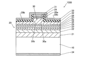
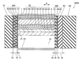
- FIG. 3 is a cross-sectional view of the semiconductor laser element on the surface along the cavity direction for explaining the structure of the semiconductor laser element according to the first embodiment of the present invention.
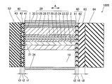
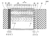
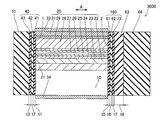
- FIG. 2 is a cross-sectional view of the nitride-based semiconductor laser device shown in FIG. 1 on a plane orthogonal to the resonator direction. It is sectional drawing in the surface along the resonator direction of the semiconductor laser element for demonstrating the structure of the semiconductor laser element by the 1st modification of 1st Embodiment of this invention. It is sectional drawing in the surface along the resonator direction of the semiconductor laser element for demonstrating the structure of the semiconductor laser element by 2nd Embodiment of this invention.
- Si having a thickness of about 100 ⁇ m and a carrier concentration of about 5 ⁇ 10 18 cm ⁇ 3 is doped.
- a semiconductor element layer 20 made of a nitride-based semiconductor having an oscillation wavelength ⁇ of about 405 nm band is formed on the substrate 10 made of n-type GaN.
- the nitride-based semiconductor laser device 1000 has a light emitting surface 1 and a light reflecting surface 2 formed at both ends in the direction in which the resonator extends (direction A), respectively.
- the light emitting surface 1 is an example of the “first resonator end surface” in the present invention
- the light reflecting surface 2 is an example of the “second resonator end surface” in the present invention.
- an end face coating film is formed on the light emitting surface 1 and the light reflecting surface 2 of the nitride semiconductor laser element 1000 by the end face coating process in the manufacturing process.
- the light emitting surface 1 of the nitride-based semiconductor laser device 1000 is approximately 10 nm in contact with the light emitting surface 1 in the order closer to the light emitting surface 1.
- An AlN film 41 having a thickness, an Al 2 O 3 film 42 having a thickness of about 10 nm in contact with the AlN film 41, and an AlN film 43 having a thickness of about 10 nm in contact with the Al 2 O 3 film 42 are laminated.
- a first alteration preventing layer 40 which is a dielectric multilayer film, is formed.
- An Al 2 O 3 film 51 having a thickness of about 70 nm is formed on the first alteration preventing layer 40 so as to be in contact with the first alteration preventing layer 40.
- the first alteration preventing layer 40 is an example of the “first insulating film” in the present invention.
- the AlN film 41 is an example of the “first nitride film” of the present invention
- the Al 2 O 3 film 42 is an example of the “first oxide film” and the “first intermediate film” of the present invention
- the AlN film 43 is an example of the “second nitride film” in the present invention.
- the Al 2 O 3 film 51 is an example of the “second oxide film” and the “second insulating film” in the present invention.
- the AlN film 41, the Al 2 O 3 film 42, and the AlN film 43 have a function of preventing the first alteration preventing layer 40 itself and the light emitting surface 1 from being altered as the laser light is emitted.
- the Al 2 O 3 film 51 has a function to control the reflectance, the laser light reflectance at the light emitting surface 1 by the Al 2 O 3 film 51 is set to have about 8%.
- the thickness t1 of the AlN film 41 is formed so that t1 ⁇ about 47 nm.
- the thickness t3 of the AlN film 43 is formed so that t3 ⁇ about 47 nm.
- the nitride films (AlN films 41 and 43) are more preferably formed to have a thickness in the range of about 1 nm to about 20 nm.
- the thickness t2 of the Al 2 O 3 film 42 is preferably formed so that t2 ⁇ about 60 nm, and more preferably has a thickness in the range of about 1 nm to about 20 nm.
- an AlN film 61 having a thickness of about 10 nm that contacts the light reflecting surface 2 is formed on the light reflecting surface 2 of the nitride-based semiconductor laser element 1000 in order of increasing distance from the light reflecting surface 2.
- a second alteration preventing layer 60 is formed which is a dielectric multilayer film in which an Al 2 O 3 film 62 having a thickness of about 10 nm that contacts the AlN film 61 is laminated.
- An SiO 2 film 63 having a thickness of about 140 nm is formed on the second alteration preventing layer 60 so as to be in contact with the Al 2 O 3 film 62.
- an SiO 2 film having a thickness of about 70 nm as a low refractive index film in contact with the SiO 2 film 63 and a ZrO 2 film having a thickness of about 50 nm as a high refractive index film are alternately arranged.
- a multilayer reflective film 64 which is a dielectric multilayer film having a thickness of about 720 nm, which is laminated by six layers, is formed.
- the multilayer reflective film 64 has a function of controlling the reflectance, and the multilayer reflective film 64 is set so that the reflectance of the laser light on the light reflecting surface 2 has a high reflectance of about 98%.
- the semiconductor element layer 20 of the nitride-based semiconductor laser element 1000 has a thickness of about 100 nm and a doping amount of about 5 ⁇ 10 18 cm ⁇ 3 on the upper surface of the substrate 10.
- An n-type layer 21 made of n-type GaN doped with Si is formed. Further, on the n-type layer 21 has a thickness of about 400 nm, n-type Si having a carrier concentration of about 5 ⁇ 10 18 cm doping amount of -3 and about 5 ⁇ 10 18 cm -3 is doped
- An n-type cladding layer 22 made of Al 0.07 Ga 0.93 N is formed.
- n-type cladding layer 22 has a thickness of about 5 nm, Si having a carrier concentration of about 5 ⁇ 10 18 cm -3 doping amount and about 5 ⁇ 10 18 cm -3 is doped n
- An n-type carrier block layer 23 made of type Al 0.16 Ga 0.84 N is formed.
- An n-type light guide layer 24 made of n-type GaN is formed.
- An active layer 25 is formed on the n-type light guide layer 24.
- the active layer 25 includes four barrier layers made of undoped In 0.02 Ga 0.98 N having a thickness of about 20 nm, and 3 layers made of undoped In 0.1 Ga 0.9 N having a thickness of about 3 nm. It has an MQW structure in which well layers of layers are alternately stacked.
- Mg having a thickness of about 100 nm, a doping amount of about 4 ⁇ 10 19 cm ⁇ 3 , and a carrier concentration of about 5 ⁇ 10 17 cm ⁇ 3 is formed on the active layer 25.
- a p-type light guide layer 26 made of p-type GaN doped with is formed.
- a p-type doped with Mg having a thickness of about 20 nm and a doping amount of about 4 ⁇ 10 19 cm ⁇ 3 and a carrier concentration of about 5 ⁇ 10 17 cm ⁇ 3.
- a p-type cap layer 27 made of Al 0.16 Ga 0.84 N is formed.
- a convex portion 28a and a flat portion 28b other than the convex portion 28a there are a convex portion 28a and a flat portion 28b other than the convex portion 28a, a doping amount of about 4 ⁇ 10 19 cm ⁇ 3 and a carrier of about 5 ⁇ 10 17 cm ⁇ 3 .
- a p-type cladding layer 28 made of p-type Al 0.07 Ga 0.93 N doped with Mg having a concentration is formed.
- the flat portion 28b of the p-type cladding layer 28 has a thickness of about 80 nm on the left and right sides of the convex portion 28a.
- the height from the upper surface of the flat portion 28b of the p-type cladding layer 28 to the upper surface of the convex portion 28a is about 320 nm, and the width of the convex portion 28a is about 1.5 ⁇ m.
- Mg having a thickness of about 10 nm, a doping amount of about 4 ⁇ 10 19 cm ⁇ 3 and a carrier concentration of about 5 ⁇ 10 17 cm ⁇ 3 is formed on the convex portion 28 a of the p-type cladding layer 28.
- the p-type contact layer 29 and the convex portion 28a of the p-type cladding layer 28 constitute a ridge portion 30 having one side surface 30a and the other side surface 30b located on the opposite side of the one side surface 30a.
- the ridge portion 30 has a width of about 1.5 ⁇ m at the lower portion and is formed in a shape extending in the [1-100] direction (the A direction in FIG. 1 which is the laser beam emission direction).
- a waveguide extending in the [1-100] direction (A direction in FIG. 1) is formed in a portion including the active layer 25 located below the ridge portion 30.
- This waveguide and the light emitting surface 1 In addition, a resonator is constituted by the light reflecting surface 2.
- Each of the p-type contact layers 29 is an example of the “semiconductor element layer” in the present invention.
- the active layer 25 is an example of the “light emitting layer” in the present invention.
- a Pt layer having a thickness of about 5 nm and a Pd having a thickness of about 100 nm are formed from the lower layer side to the upper layer side.
- a p-side ohmic electrode 31 in which a layer and an Au layer having a thickness of about 150 nm are formed in this order is formed.
- a current blocking layer 32 made of a SiO 2 film (insulating film) having a thickness of about 250 nm is formed on a region other than the upper surface of the p-side ohmic electrode 31.
- a predetermined region on the current blocking layer 32 has a Ti layer having a thickness of about 100 nm and a thickness of about 100 nm from the lower layer side toward the upper layer side so as to be in contact with the upper surface of the p-side ohmic electrode 31.
- an n-side electrode 34 is formed on the lower surface of the n-type GaN substrate 10.
- the n-side electrode 34 includes an Al layer having a thickness of about 10 nm, a Pt layer having a thickness of about 20 nm, and an Au layer having a thickness of about 300 nm, which are stacked in order from the lower surface side of the n-type GaN substrate 10. It is composed of
- an n-type layer 21 having a thickness of about 100 nm, an n-type cladding layer 22 having a thickness of about 400 nm are formed on a substrate 10 using a metal organic vapor phase epitaxy (MOVPE) method.
- An n-type carrier block layer 23 having a thickness of about 5 nm, an n-type light guide layer 24 having a thickness of about 100 nm, and an active layer 25 having a total thickness of about 90 nm are sequentially formed.
- the active layer 25 has a p-type light guide layer 26 having a thickness of about 100 nm, a p-type cap layer 27 having a thickness of about 20 nm, a p-type cladding layer 28 having a thickness of about 400 nm, and a thickness of about 10 nm.
- the p-type contact layer 29 is formed sequentially. Then, after performing the p-type annealing treatment and the formation of the ridge portion 30 by etching, the p-side ohmic electrode 31, the current blocking layer 32, and the p-side pad electrode 33 are formed by vacuum deposition. Further, the n-side electrode 34 is formed on the lower surface of the substrate 10 by vacuum deposition.
- scribe scratches are formed in a direction perpendicular to the direction in which the ridge portion 30 extends (direction A in FIG. 1) by laser or mechanical scribing at a predetermined location. This scribe flaw is formed in a broken line shape in a portion excluding the ridge portion 30.
- the substrate 10 on which the above-described semiconductor laser structure is formed is cleaved along the scribe scratches to form a structure separated into a bar state. Thereafter, the bar-shaped substrate on which the cleavage plane is formed is introduced into an electron cyclotron resonance (ECR) sputtering film forming apparatus.
- ECR electron cyclotron resonance
- the light emitting surface 1 is cleaned by irradiating the light emitting surface 1 (see FIG. 1) formed of a cleaved surface with ECR plasma.
- the ECR plasma is generated in an N 2 gas atmosphere.
- the light emitting surface 1 (see FIG. 1) is slightly etched.
- RF power is not applied to the sputtering target.
- the first alteration preventing layer 40 and the Al 2 O 3 film 51 (see FIG. 1) are sequentially formed on the light emitting surface 1 by ECR sputtering.
- the light reflecting surface 2 is cleaned by irradiating the light reflecting surface 2 (see FIG. 1) made of a cleaved surface with ECR plasma. At this time, the light reflecting surface 2 is slightly etched. At that time, RF power is not applied to the sputtering target. Thereafter, the second alteration preventing layer 60, the SiO2 film 63, and the multilayer reflective film 64 (see FIG. 1) are formed on the light reflecting surface 2 by ECR sputtering.
- the bar-shaped substrate 10 is separated in a direction parallel to the direction in which the ridge portion 30 extends (direction A in FIG. 1), thereby forming the nitride-based semiconductor laser device 1000 in a chip form.
- the nitride semiconductor laser element 1000 in which the generation of COD is suppressed can be easily formed.
- the nitride semiconductor laser element 1000 according to the first embodiment is formed.
- a prevention layer 40 is provided.
- the AlN film 43 disposed on the outside makes it difficult for oxygen present in the Al 2 O 3 film 51 and the atmosphere to be taken into the first alteration preventing layer 40, so the Al 2 O 3 film 42 and the AlN film Desorption of oxygen at the interface with 41, a substitution reaction between oxygen and nitrogen, and the like are suppressed. That is, the interface between the Al 2 O 3 film 42 and the AlN film 41 is prevented from being altered and deteriorated.
- the reliability of the nitride-based semiconductor laser device 1000 can be improved.
- the above effect is particularly effective for a semiconductor laser element that emits laser light having a short oscillation wavelength of about 525 nm or less and high energy.
- the altered region that spreads in the Al 2 O 3 film 42 by the AlN film 43 is formed as Al 2. Since it can remain in the O 3 film 42, expansion of alteration is suppressed. Thereby, the alteration of the first alteration preventing layer 40 can be minimized.
- the thickness of the Al 2 O 3 film 51 formed on the first alteration preventing layer 40 that is, on the surface of the first alteration preventing layer 40 located on the side opposite to the light emitting surface 1
- the reflectance of the laser beam emitted from the light emitting surface 1 can be easily controlled.
- the reliability of the nitride-based semiconductor laser device 1000 corresponding to high output can be improved.
- the thickness t1 of the AlN film 41, the thickness t2 of the Al 2 O 3 film 42, and the thickness t3 of the AlN film 43 constituting the first alteration preventing layer 40 are t1 ⁇ / (4 ⁇ n1) and t2 ⁇ , respectively.
- the thickness of each film constituting the first alteration preventing layer 40 is larger than ⁇ / (4 ⁇ n). Get smaller. Thereby, the laser light emitted from the light emitting surface 1 is transmitted without being affected by the thickness of each film constituting the first alteration preventing layer 40 and reaches the Al 2 O 3 film 51.
- the reflectance control function of the Al 2 O 3 film 51 set to have a desired reflectance (about 8%) can be easily suppressed from being affected by the first alteration preventing layer 40.
- the thickness of each film constituting the first alteration preventing layer 40 is thin, film peeling (peeling) caused by stress after the film formation can be suppressed.
- the AlN film 41 of the first alteration preventing layer 40 is in contact with the semiconductor element layer 20. Thereby, since the AlN film 41 is in contact with the light emitting surface 1, the AlN film 41 can easily suppress the oxygen of the Al 2 O 3 film 42 from being taken into the semiconductor element layer 20.
- the AlN film 41 and the AlN film 43 and the Al 2 O 3 film 42 contain the same Al element.
- the AlN film 41 and the Al 2 O 3 film 42 that are in contact with each other, and the AlN film 43 and the Al 2 O 3 film 42 that are in contact with each other are materials containing the same kind of metal element (Al element), respectively. Therefore, the adhesion at the time of contact can be improved. As a result, film peeling (peeling) of the AlN film 41 and the AlN film 43 can be suppressed.
- the AlN film 41 and the AlN film 43 each contain Al. Thereby, since the nitride containing Al has good insulation, the insulation of the AlN film 41 and the AlN film 43 can be improved. In addition, it is possible to effectively suppress oxygen from being taken into the first alteration preventing layer 40 and the semiconductor element layer 20 by the nitride film containing Al.
- the Al 2 O 3 film 42 contains Al.
- the oxide containing Al has good insulation, the insulation of the Al 2 O 3 film 42 can be improved.
- the Al 2 O 3 film 42 containing Al since the Al 2 O 3 film 42 containing Al, the AlN film 41 and the AlN film 43 sandwiching the Al 2 O 3 film 42 from both sides can be easily brought into contact with the same kind of metal element (Al element), The adhesion between each film can be improved.
- the semiconductor element layer 20 including the active layer 25 is made of a nitride-based semiconductor.
- the nitride-based semiconductor laser device 1000 having a short oscillation wavelength of about 405 nm band and emitting high-energy laser light the resonator end face on the light emission side caused by heat generation particularly when laser light is emitted Destruction of (light emitting surface 1) can be effectively suppressed.
- the thickness t5 of the AlN film 61 and the thickness t6 of the Al 2 O 3 film 62 constituting the second alteration preventing layer 60 are set to t5 ⁇ / (4 ⁇ n5) and t6 ⁇ , respectively.
- the thickness of each film constituting the second alteration preventing layer 60 becomes smaller than ⁇ / (4 ⁇ n). Thereby, the laser light emitted from the light reflecting surface 2 is transmitted without being affected by the thickness of each film constituting the second alteration preventing layer 60.
- the thickness t8 of the SiO 2 film 63 is set to be t8 ⁇ / (2 ⁇ n8), the laser light is not substantially reflected even in the SiO 2 film 63.
- the reflectance control function of the multilayer reflective film 64 set to have a desired reflectance (about 98%) can be easily suppressed from being influenced by the second alteration preventing layer 60.
- each film constituting the second alteration preventing layer 60 is thin, film peeling (peeling) due to stress after film formation can be suppressed.
- an SiO 2 film 52 having a thickness of about 95 nm is formed so as to be in contact with the first alteration preventing layer 40.
- the SiO 2 film 52 is an example of the “second oxide film” and the “second insulating film” in the present invention.
- the remaining structure and manufacturing process of the nitride-based semiconductor laser device 1005 according to the first modification of the first embodiment are the same as those of the first embodiment.
- the first alteration preventing layer 40 is formed, that is, on the surface of the first alteration preventing layer 40 located on the side opposite to the light emitting surface 1.
- the thickness of the SiO 2 film 52 By adjusting the thickness of the SiO 2 film 52, the reflectance of the laser light emitted from the light emitting surface 1 can be easily controlled.
- the reliability of the nitride-based semiconductor laser device 1005 corresponding to high output can be improved.
- the remaining effects of the first modification are similar to those of the aforementioned first embodiment.
- an AlO X N Y film 44 that is an oxynitride film is used in place of the Al 2 O 3 film 42 used in the first embodiment, and the first alteration is performed.
- a case where an AlO X N Y film 45 that is an oxynitride film is used between the prevention layer 40 and the Al 2 O 3 film 51 will be described.
- the AlO X N Y film 44 is an example of the “first oxynitride film” and the “first intermediate film” in the present invention.
- the AlO X N Y film 45 is an example of the “third oxynitride film” and the “second intermediate film” in the present invention.
- the AlO X N Y film 44 and the AlO X N Y film 45 are described as the AlON film 44 and the AlON film 45, respectively.
- the second embodiment on the light emitting surface 1 of the nitride-based semiconductor laser device 2000, about 10 nm in contact with the light emitting surface 1 in order from the light emitting surface 1.
- a certain first alteration preventing layer 240 is formed.
- an AlON film 45 having a thickness of about 10 nm and an Al 2 O 3 film 51 having a thickness of about 70 nm are formed on the first alteration preventing layer 240 so as to be in contact with the first alteration preventing layer 240.
- the first alteration preventing layer 240 is an example of the “first insulating film” in the present invention.
- the thicknesses t2 and t4 of the AlON films 44 and 45 are t2 ⁇ about 47 nm to about 60 nm, and t4 ⁇ It is preferably formed in the range of about 47 nm to about 60 nm.
- the refractive index of AlON is determined in the range of about 1.68 to about 2.15 depending on the mixing ratio of Al 2 O 3 and AlN
- the thicknesses t2 and t4 of the AlON films 44 and 45 are: The above range exists.
- the oxynitride films (AlON films 44 and 45) more preferably have a thickness in the range of about 1 nm to about 20 nm.
- the remaining structure and manufacturing process of the nitride-based semiconductor laser device 2000 according to the second embodiment are the same as those of the first embodiment.
- the first alteration preventing layer 240 in which the AlN film 41, the AlON film 44, and the AlN film 43 are formed on the light emitting surface 1 in order from the light emitting surface 1. Is provided. Accordingly, oxygen present in the AlON film 44 and in the atmosphere is less likely to be taken into the first alteration preventing layer 240 by the AlN film 43 disposed on the outer side, so that oxygen at the interface between the AlON film 44 and the AlN film 41 is prevented. And the substitution reaction between oxygen and nitrogen are suppressed. That is, the interface between the AlON film 44 and the AlN film 41 is prevented from being altered and deteriorated.
- the oxynitride film such as the AlON film 44 has a smaller oxygen atom content than the oxide film such as the Al 2 O 3 film, the above reaction is considered to be lighter. Therefore, even when the output power of the laser beam is increased, the heat generation in the vicinity of the light emitting surface 1 and the first alteration preventing layer 240 is suppressed, so that the destruction of the resonator end surface (light emitting surface 1) is further suppressed. As a result, the reliability of the nitride semiconductor laser element 2000 can be further improved.
- the thickness t1 of the AlN film 41, the thickness t2 of the AlON film 44, and the thickness t3 of the AlN film 43 constituting the first alteration preventing layer 240 are respectively t1 ⁇ / (4 ⁇ n1) and t2 ⁇ / ( By setting so that 4 ⁇ n2) and t3 ⁇ / (4 ⁇ n3), the thickness of each film constituting the first alteration preventing layer 240 becomes smaller than ⁇ / (4 ⁇ n). Thereby, the laser light emitted from the light emitting surface 1 is transmitted without being affected by the thickness of each film constituting the first alteration preventing layer 240 and reaches the Al 2 O 3 film 51.
- the reflectance control function of the Al 2 O 3 film 51 set to have a desired reflectance (about 8%) can be easily suppressed from being affected by the first alteration preventing layer 240. Moreover, since the thickness of each film constituting the first alteration preventing layer 240 is thin, film peeling (peeling) caused by stress after film formation can be suppressed.
- an AlON film 45 that is an oxynitride film is further formed between the first alteration preventing layer 240 and the Al 2 O 3 film 51.
- a region composed of the AlN film 41 and the AlON film 44 and a region composed of the AlN film 43 and the AlON film 45 are formed on the light emitting surface 1 in order from the light emitting surface 1 to be multilayered. Therefore, it is possible to further suppress the breakage of the resonator end face (light emitting surface 1) on the light emitting side.
- the thickness t4 of the AlON film 45 is also set to satisfy t4 ⁇ / (4 ⁇ n4).
- the laser beam of the light emitting surface 1 emits reaches the the Al 2 O 3 film 51 passes through without being also affected by the thickness of the AlON film 45.
- the reflectance control function of the Al 2 O 3 film 51 for controlling the reflectance can be easily suppressed from being affected by the first alteration preventing layer 240.
- the AlON film 44 contains Al. Thereby, since the oxynitride containing Al has good insulation, the insulation of the AlON film 44 can be improved. Further, since the AlN film 44 and the AlN film 41 and AlN film 43 sandwiching the AlON film 44 from both sides can be easily brought into contact with the same kind of metal element (Al element), the adhesion between the respective films is improved. Can be made. The remaining effects of the second embodiment are similar to those of the aforementioned first embodiment.
- the second alteration preventing layer which is a dielectric multilayer film in which a nitride film and an oxide film are multilayered on the light reflection surface 2 side.
- the second alteration preventing layer 160 is an example of the “third insulating film” in the present invention.
- the light reflecting surface 2 of the nitride-based semiconductor laser element 3000 is contacted with the light reflecting surface 2 in an order of about 10 nm.
- An AlN film 61 having a thickness, an Al 2 O 3 film 62 having a thickness of about 10 nm in contact with the AlN film 61, and an AlN film 73 having a thickness of about 10 nm in contact with the Al 2 O 3 film 62 are laminated.
- a second alteration preventing layer 160 which is a dielectric multilayer film is formed.
- the AlN film 61 is an example of the “third nitride film” of the present invention
- the Al 2 O 3 film 62 is an example of the “fourth oxide film” and the “third intermediate film” of the present invention
- the AlN film 73 is an example of the “fourth nitride film” in the present invention.
- the AlN film 61, the Al 2 O 3 film 62, and the AlN film 73 have a function of preventing the second alteration preventing layer 160 itself and the light reflecting surface 2 from being altered due to the reflection of the laser light. Have.
- SiO having a thickness of about 140 nm so as to contact the AlN film 73 is formed on the second alteration preventing layer 160.
- Two films 63 are formed on the SiO 2 film 63.
- an SiO 2 film having a thickness of about 70 nm as a low refractive index film in contact with the SiO 2 film 63 and a ZrO 2 film having a thickness of about 50 nm as a high refractive index film are alternately arranged.
- a multilayer reflective film 64 which is a dielectric multilayer film having a thickness of about 720 nm, which is laminated by six layers, is formed.
- the thickness t5 of the AlN film 61 is formed so that t5 ⁇ about 47 nm.
- the thickness t6 of the AlN film 73 is preferably formed so that t6 ⁇ about 47 nm.
- the nitride films (AlN films 61 and 73) are more preferably formed to have a thickness in the range of about 1 nm to about 20 nm.
- the thickness t7 of the Al 2 O 3 film 62 is preferably formed so that t7 ⁇ about 60 nm, and more preferably has a thickness in the range of about 1 nm to about 20 nm.
- the remaining structure and manufacturing process of the nitride-based semiconductor laser device 3000 according to the third embodiment are the same as those of the first embodiment.
- a prevention layer 160 is provided.
- the AlN film 73 disposed on the outside makes it difficult for oxygen present in the multilayer reflective film 64 made of oxide and in the atmosphere to be taken into the second alteration preventing layer 160, so that the Al 2 O 3 film 62 and It is suppressed that the interface with the AlN film 61 is altered and deteriorated.
- the reliability of the nitride based semiconductor laser device 3000 can be further improved.
- the thickness t5 of the AlN film 61, the thickness t6 of the Al 2 O 3 film 62, and the thickness t7 of the AlN film 73 constituting the second alteration preventing layer 160 are t5 ⁇ / (4 ⁇ n5) and t6 ⁇ , respectively.
- the thickness of each film constituting the second alteration preventing layer 160 is larger than ⁇ / (4 ⁇ n). Get smaller. Thereby, the laser light once emitted from the light reflecting surface 2 is transmitted without being influenced by the thickness of each film constituting the second alteration preventing layer 160 and reaches the multilayer reflecting film 64.
- the reflectance control function of the multilayer reflective film 64 set to have a desired reflectance is influenced by the second alteration preventing layer 160.
- the thickness of each film constituting the second alteration preventing layer 160 is thin, film peeling (peeling) due to stress after film formation can be suppressed.
- the AlN film 61 of the second alteration preventing layer 160 is in contact with the semiconductor element layer 20. Therefore, since the AlN film 61 is in contact with the light reflecting surface 2, the AlN film 61 can easily suppress the oxygen of the Al 2 O 3 film 62 from being taken into the semiconductor element layer 20.
- the AlN film 61 and the AlN film 73 and the Al 2 O 3 film 62 contain the same Al element. Accordingly, the AlN film 61 and the Al 2 O 3 film 62 that are in contact with each other, and the AlN film 73 and the Al 2 O 3 film 62 that are in contact with each other are materials containing the same kind of metal element (Al element), respectively. Therefore, the adhesion at the time of contact can be improved. As a result, film peeling (peeling) of the AlN film 61 and the AlN film 73 can be suppressed.
- Al element metal element
- the AlN film 61 and the AlN film 73 each contain Al.
- the nitride containing Al has good insulation, the insulation of the AlN film 61 and the AlN film 73 can be improved.
- the nitride film containing Al can effectively prevent oxygen from being taken into the second alteration preventing layer 160 and the semiconductor element layer 20.
- the Al 2 O 3 film 62 contains Al. Thereby, since the oxide containing Al has good insulation, the insulation of the Al 2 O 3 film 62 can be improved. Further, since the Al 2 O 3 film 62 and the AlN film 61 and AlN film 73 sandwiching the Al 2 O 3 film 62 from both sides contain a common element (Al), the adhesion between the films is improved. Can be made.
- the multilayer reflective film 64 is provided on the second alteration preventing layer 160 via the SiO 2 film 63 in contact with the AlN film 73. Thereby, by adjusting the thickness of the multilayer reflective film 64, the reflectance of the laser light emitted from the second alteration preventing layer 160 on the light reflecting surface 2 can be easily controlled.
- the remaining effects of the third embodiment are similar to those of the aforementioned first embodiment.
- the first alteration preventing layer 340 constituting the nitride semiconductor laser element 4000 includes two nitride films and the two nitride films.
- the second alteration preventing layer 260 includes a structure in which a nitride film, an oxynitride film, and an oxide film are sequentially stacked.
- the light emitting surface 1 is contacted with the light emitting surface 1 in the order closer to the light emitting surface 1.
- An AlN film 41 having a thickness
- an AlON film 81 having a thickness of about 5 nm in contact with the AlN film 41
- an Al 2 O 3 film 82 having a thickness of about 2.5 nm in contact with the AlON film 81
- the first alteration preventing layer which is a dielectric multilayer film in which an AlON film 83 having a thickness of about 2.5 nm in contact with the three films 82 and an AlN film 43 having a thickness of about 10 nm in contact with the AlON film 83 are laminated.
- the Al 2 O 3 film 51 having a thickness of about 73 nm is formed on the first alteration preventing layer 340 so as to be in contact with the first alteration preventing layer 340.
- the AlON film 81, the Al 2 O 3 film 82, and the AlON film 83 are examples of the “first intermediate film” of the present invention, and the “first oxynitride film” and the “first oxidation film” of the present invention, respectively. It is an example of “film” and “first oxynitride film”.
- the Al 2 O 3 film 51 is set so that the reflectance of the laser beam on the light emitting surface 1 is about 8%.
- the average refractive index of the AlON film 81, Al 2 O 3 film 82 and the AlON film 83 is n2
- the average refractive index n2 of the multilayer film composed of the three layers (AlON film 81, Al 2 O 3 film 82 and AlON film 83) is about 1.68 to about 1, depending on the mixing ratio of Al 2 O 3 and AlN.
- the total thickness t2 is t2 ⁇ about 47 nm (AlN is about 100%) to about 60 nm (Al 2 O 3 is It is preferably formed in a range of about 100%, and more preferably formed to have a thickness in the range of about 1 nm to about 20 nm.
- the light-reflecting surface 2 of the nitride-based semiconductor laser element 4000 has an AlN film 61 having a thickness of about 10 nm in contact with the light reflecting surface 2 in order from the light reflecting surface 2;
- a second alteration preventing film which is a dielectric multilayer film in which an AlON film 84 having a thickness of about 5 nm in contact with the AlN film 61 and an Al 2 O 3 film 85 having a thickness of about 5 nm in contact with the AlON film 84 are laminated.
- Layer 260 is formed.
- An SiO 2 film 63 having a thickness of about 140 nm is formed on the second alteration preventing layer 260 so as to be in contact with the Al 2 O 3 film 85.
- an SiO 2 film having a thickness of about 70 nm as a low refractive index film in contact with the SiO 2 film 63 and a ZrO 2 film having a thickness of about 50 nm as a high refractive index film are alternately arranged.
- a multilayer reflective film 64 which is a dielectric multilayer film having a thickness of about 720 nm, which is laminated by six layers, is formed. Further, the multilayer reflective film 64 is set so that the reflectance of the laser light on the light reflecting surface 2 has a high reflectance of about 98%.
- 5 nm) is set to have a relationship of t5 ⁇ / (4 ⁇ n5), t6 ⁇ / (4 ⁇ n6), and t9 ⁇ / (4 ⁇ n9), respectively.
- the remaining structure and manufacturing process of the nitride-based semiconductor laser device 4000 according to the fourth embodiment are the same as those of the first embodiment.
- the AlON film 81, the Al 2 O 3 film 82, and the AlON film 83 are formed between the AlN film 41 and the AlN film 43.
- oxygen present in the Al 2 O 3 film 51 and in the atmosphere is further less likely to be taken into the first alteration preventing layer 340, and the interface between the AlON film 81 and the AlN film 41 is altered and deteriorated. Can be further suppressed.
- the AlON film 81 and the AlON film 83 are formed between the AlN film 41 and the AlN film 43 so as to sandwich the Al 2 O 3 film 82 in the stacking direction.
- the first alteration preventing layer 340 includes a nitride film (AlN film 41), an oxynitride film (AlON film 81), an oxide film (Al 2 O 3 film 82), an oxynitride film (AlON film 83), and a nitride film. Since the (AlN film 43) is laminated in this order, the composition in the first alteration preventing layer 340 gradually changes. As a result, the adhesion between the respective films in the first alteration preventing layer 340 can be further improved, so that the strength of the first alteration preventing layer 340 composed of a plurality of thin films can be maintained.
- the thickness t5 of the AlN film 61, the thickness t6 of the AlON film 84, and the thickness t9 of the Al 2 O 3 film 85 constituting the second alteration preventing layer 260 are set to t5 ⁇ / (4 Xn5), t6 ⁇ / (4 ⁇ n6) and t9 ⁇ / (4 ⁇ n9), so that the thickness of each film constituting the second alteration preventing layer 260 is ⁇ / ( 4 ⁇ n).
- the laser light emitted from the light reflecting surface 2 is transmitted without being affected by the thickness of each film constituting the second alteration preventing layer 260.
- the remaining effects of the fourth embodiment are similar to those of the aforementioned first embodiment.
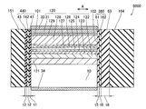
- the fifth embodiment on the light emitting surface 1 of the nitride-based semiconductor laser device 5000, approximately 10 nm in contact with the light emitting surface 101 in order from the light emitting surface 101.
- a dielectric multilayer in which an AlN film 41 having a thickness, an HfO 2 film 142 having a thickness of about 10 nm in contact with the AlN film 41, and an AlN film 43 having a thickness of about 10 nm in contact with the HfO 2 film 142 are laminated.
- a first alteration preventing layer 440 that is a film is formed.
- An HfO 2 film 151 having a thickness of about 100 nm is formed on the first alteration preventing layer 440 so as to be in contact with the first alteration preventing layer 440.
- the first alteration preventing layer 440 is an example of the “first insulating film” in the present invention.
- the HfO 2 film 142 is an example of the “first oxide film” and the “first intermediate film” in the present invention, and the HfO 2 film 151 is the “second oxide film” and the “second insulating film” in the present invention. Is an example.
- the HfO 2 film 151 is set so that the reflectance of the laser beam at the light exit surface 101 is about 8%.
- the thickness t1 of the AlN film 41 is preferably formed so that t1 ⁇ about 42 nm.
- the thickness t3 of the AlN film 43 is preferably formed so that t3 ⁇ about 42 nm.
- the nitride films (AlN films 41 and 43) are more preferably formed to have a thickness in the range of about 1 nm to about 20 nm.
- the thickness t2 of the HfO 2 film 142 is preferably formed so that t2 ⁇ about 47 nm, and more preferably has a thickness in the range of about 1 nm to about 20 nm.
- an AlN film 61 having a thickness of about 10 nm in contact with the light reflecting surface 102 is formed on the light reflecting surface 102 of the nitride-based semiconductor laser element 5000 in order from the light reflecting surface 102.
- a second alteration preventing layer 360 is formed, which is a dielectric multilayer film in which an HfO 2 film 162 having a thickness of about 10 nm contacting the AlN film 61 is laminated.
- an SiO 2 film 63 having a thickness of about 100 nm that is in contact with the HfO 2 film 162 is formed.
- the HfO 2 film is eight layers alternately having a thickness of about 40nm as an SiO 2 film and the high refractive index film having a thickness of about 70nm as a low refractive index film in contact with the SiO 2 film
- ⁇ / (4 ⁇ n5), t6 ⁇ / (4 ⁇ n6) and t8 ⁇ / (2 ⁇ n8) are set.
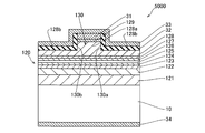
- the semiconductor element layer 120 of the nitride-based semiconductor laser element 5000 has a thickness of about 100 nm on the upper surface of the substrate 10 made of n-type GaN and has a thickness of about 5 ⁇ 10 18 cm.
- An n-type layer 121 made of Ge-doped n-type GaN having a doping amount of ⁇ 3 is formed.
- An n-type cladding layer 122 made of Al 0.10 Ga 0.90 N is formed.
- An n-side carrier block layer 123 made of undoped Al 0.20 Ga 0.80 N having a thickness of about 10 nm is formed on the n-type cladding layer 122. Further, on the n-side carrier blocking layer 123 has a thickness of about 150 nm, Ge having a carrier concentration of about 5 ⁇ 10 18 cm -3 doping amount and about 5 ⁇ 10 18 cm -3 is doped An n-type light guide layer 124 made of n-type Al 0.03 Ga 0.97 N is formed. An active layer 125 is formed on the n-type light guide layer 124.
- This active layer 125 has two barrier layers made of undoped Al 0.06 Ga 0.94 N having a thickness of about 10 nm and single well layers made of undoped GaN having a thickness of about 18 nm alternately. It has a stacked SQW structure.
- Mg having a thickness of about 150 nm, a doping amount of about 3 ⁇ 10 19 cm ⁇ 3 , and a carrier concentration of about 7 ⁇ 10 17 cm ⁇ 3 is formed on the active layer 125.
- a p-type light guide layer 126 made of p-type Al 0.03 Ga 0.97 N doped with is formed on the p-type light guide layer 126.
- a p-side carrier block layer 127 having a thickness of about 10 nm and made of undoped Al 0.20 Ga 0.80 N is formed.
- a convex portion 128a and a flat portion 128b other than the convex portion 128a there are a convex portion 128a and a flat portion 128b other than the convex portion 128a, a doping amount of about 3 ⁇ 10 19 cm ⁇ 3 , and about 7 ⁇ 10 17 cm ⁇ 3 .
- a p-type cladding layer 128 made of p-type Al 0.10 Ga 0.90 N doped with Mg having a carrier concentration is formed.
- the flat portion 128b of the p-type cladding layer 128 has a thickness of about 80 nm on the left and right sides of the convex portion 128a.
- the height from the upper surface of the flat portion 128b of the p-type cladding layer 128 to the upper surface of the convex portion 128a is about 320 nm, and the width of the convex portion 128a is about 1.5 ⁇ m.
- Mg having a thickness of about 10 nm, a doping amount of about 4 ⁇ 10 19 cm ⁇ 3 , and a carrier concentration of about 5 ⁇ 10 17 cm ⁇ 3 is formed on the convex portion 128 a of the p-type cladding layer 128.
- the p-type contact layer 129 and the convex portion 128a of the p-type cladding layer 128 constitute a ridge portion 130 having one side surface 130a and the other side surface 130b located on the opposite side of the one side surface 130a.
- the ridge portion 130 has a width of about 1.5 ⁇ m at the lower portion and is formed in a shape extending in the [1-100] direction (A direction of FIG. 7 which is the laser beam emission direction).
- a waveguide extending in the [1-100] direction (A direction in FIG. 7) is formed in a portion including the active layer 125 located below the ridge portion 130. This waveguide and the light emitting surface 101 are formed.
- the light reflecting surface 102 constitutes a resonator.
- the p-type contact layer 129 is an example of the “semiconductor element layer” in the present invention.
- the active layer 125 is an example of the “light emitting layer” in the present invention.
- the other structure and manufacturing process of the nitride semiconductor laser element 5000 according to the fifth embodiment are the same as those of the first embodiment.
- the Al 2 O 3 film 42 used in the first embodiment is used as the first oxide film and the second oxide film of the end surface coat film formed on the light emitting surface 101.
- HfO 2 films 142 and 151 are used, respectively.
- the HfO 2 film 162 is used instead of the Al 2 O 3 film 62 used in the first embodiment.
- an HfO 2 film is used instead of the Al 2 O 3 film used in the first embodiment.
- the film stress of the HfO 2 film can be easily made smaller than the film stress of Al 2 O 3 , the peeling on each end face coat film formed on the light emitting surface 101 and the light reflecting surface 102 is further reduced. Can be suppressed. Furthermore, since the film density of the HfO 2 film can be easily made larger than the film density of Al 2 O 3 , it is possible to further suppress deterioration that occurs when high-energy laser light is irradiated. As a result, the reliability of the nitride-based semiconductor laser device 5000 can be further improved. Other effects of the fifth embodiment are the same as those of the first embodiment.
- the semiconductor element layer 20 (120) is shown as an example of a nitride-based semiconductor layer.
- the present invention is not limited to this, and the semiconductor element layer is not limited to the nitride.
- You may comprise by semiconductor layers other than a type
- the first nitride film (AlN film 41) and the second nitride film (AlN film 43) are shown as AlN films.
- the present invention is not limited to this.
- the first and second nitride films may be formed of a nitride containing Si element or the like.
- nitride films made of Si 3 N 4 can be used for the first nitride film and the second nitride film, respectively.
- the thickness t of the first nitride film and the second nitride film is formed so that t ⁇ about 48 nm. It is particularly preferred to have a thickness in the range of about 1 nm to about 20 nm.
- first nitride film 41 AlN film 41
- second nitride film AlN film 43
- present invention is not limited to this.
- the first nitride film and the second nitride film may be nitride films containing different metal elements.
- the first oxide film (Al 2 O 3 film 42) is an Al 2 O 3 film.
- the present invention is not limited to this, and the first oxide film is not limited thereto.
- the film may be formed of an oxide containing Si element, Zr element, Ta element, Hf element, Nb element, and the like.
- the thickness t of the first oxide film is preferably formed to be t ⁇ about 68 nm.
- the thickness t of the first oxide film is preferably formed so that t ⁇ about 44 nm.
- the thickness t of the first oxide film is preferably formed so that t ⁇ about 45 nm.
- the thickness t of the first oxide film is preferably formed to be t ⁇ about 47 nm.
- the thickness t of the first oxide film is preferably formed to be t ⁇ about 43 nm.
- each of the first oxide films exemplified above is particularly preferably formed to have a thickness in the range of about 1 nm to about 20 nm.
- the first oxynitride film (AlON film 44) is an AlON film
- the present invention is not limited to this, and the oxynitride film is not limited to an acid containing Si element or the like. You may form by nitride.
- the first oxynitride film is an oxynitride film made of SiO X N Y (hereinafter referred to as SiON)
- the refractive index of SiON is a mixture of SiO 2 and Si 3 N 4.
- the thickness t of the first oxynitride film is determined to be about 1.48 to about 2.1 depending on the ratio, so that the thickness t of the first oxynitride film is t ⁇ about 48 nm (SiO 2 is about 100%) to about 68 nm (Si 3 N 4 It is preferably formed in a range of about 100%, and more preferably formed to have a thickness in the range of about 1 nm to about 20 nm.
- the first intermediate film formed between the first nitride film (AlN film 41) and the second nitride film (AlN film 43) is the first oxide film (Al 2 O 3 film).
- the present invention is not limited to this example.
- Other combinations in which the first intermediate film includes both the first oxide film and the first oxynitride film, such as one intermediate film including the first oxide film and the first oxynitride film, may be used.
- the third oxynitride film (AlON film 45) is used as the second intermediate film between the second nitride film (AlN film 43) and the second oxide film (Al 2 O 3 film 51).
- an oxide film such as an Al 2 O 3 film or a SiO 2 film may be formed as the second intermediate film.
- the oxide film such as the Al 2 O 3 film or the SiO 2 film used as the second intermediate film is an example of the “third oxide film” in the present invention.
- the second intermediate film may include both the third oxynitride film and the third oxide film.
- the present invention is not limited to this.
- the first oxynitride film and the third oxynitride film may be oxynitride films containing different metal elements.
- the second insulating film may be an oxynitride film such as an AlON film or a SiON film.
- the oxynitride film such as the AlON film or the SiON film used as the second insulating film is an example of the “second oxynitride film” in the present invention.
- the second insulating film may be configured to include both the second oxide film and the second oxynitride film.
- the Al 2 O 3 film 51 that controls the reflectance of the light emitting surface 1 is formed to have a thickness of about 70 nm or about 73 nm (about 60 nm in the second embodiment). Although shown, the present invention is not limited to this, and the Al 2 O 3 film 51 may be formed to have a thickness other than the above.
- the thickness of the SiO 2 film 52 that controls the reflectance of the light emitting surface 1 is about 70 nm is shown, but the present invention is not limited to this.
- the SiO 2 film 52 may be formed to have a thickness other than the above.
- the present invention is not limited to this.
- the third and fourth nitride films may be formed of a nitride containing Si element or the like. Also in this modification, for example, nitride films made of Si 3 N 4 can be used for the third nitride film and the fourth nitride film, respectively.
- the thickness t of the third nitride film and the fourth nitride film is formed so that t ⁇ about 48 nm. It is particularly preferred to have a thickness in the range of about 1 nm to about 20 nm.
- the present invention is not limited to this, and the third embodiment
- the nitride film and the fourth nitride film may be a nitride film containing different metal elements.
- the fourth oxide film (Al 2 O 3 film 62) is an Al 2 O 3 film
- the present invention is not limited to this, and the fourth oxide film is Similar to the first oxide film (Al 2 O 3 film 42) of the first embodiment, it may be formed of an oxide containing Si element, Zr element, Ta element, Hf element, Nb element, and the like. In this case, the thickness of the fourth oxide film can be set similarly to the first oxide film of the first embodiment.
- the fourth oxide film (Al 2 O 3 film 62) sandwiched between the third nitride film (AlN film 61) and the fourth nitride film (AlN film 73) is formed.
- the present invention is not limited to this, and a third intermediate film made of an oxynitride film such as an AlON film or a SiON film may be formed between the third nitride film and the fourth nitride film.
- the oxynitride film such as an AlON film or SiON film used as the third intermediate film is an example of the “fourth oxynitride film” in the present invention.
- the thickness t of the fourth oxynitride film is formed in the range of t ⁇ about 47 nm to about 60 nm. In particular, it is more preferable to have a thickness in the range of about 1 nm to about 20 nm.
- the thickness t of the fourth oxynitride film is t ⁇ about 48 nm (SiO 2 is about 100%) to about 68 nm (Si 3 N 4 is about 100%).
- each film contains a common element (Al), so that the adhesion between the films is improved. Can be improved.
- the third intermediate film sandwiched between the third nitride film (AlN film 61) and the fourth nitride film (AlN film 73) is the fourth oxide film (Al 2 O 3 film 62).
- the present invention is not limited to this, and the third intermediate film may include both the fourth oxide film and the fourth oxynitride film.
- the multilayer reflective film 64 for controlling the reflectance on the light reflecting surface 2 side is formed by alternately laminating six layers of SiO 2 films and ZrO 2 films.
- the present invention is not limited to this, and the SiO 2 film and the ZrO 2 film may be alternately stacked in a number other than six layers.
- the multilayer reflective film two different kinds of insulating films having other refractive indexes than the SiO 2 film and the ZrO 2 film may be combined.
- the first oxide film (HfO 2 film 142) and the second oxide film (HfO 2 film 162) of the end face coating film on the light emitting surface 101 of the ultraviolet semiconductor laser 5000 are replaced with the HfO 2 film.
- MgO and Y 2 O 3 oxynitrides (TaO X N Y , MgO X N Y and YO X N Y etc.).
- the second alteration preventing layer 360 of the end surface coating film on the light reflecting surface 102 of the ultraviolet semiconductor laser 5000 and the oxide film in the multilayer reflecting film 164 are composed of an HfO 2 film.
- oxynitrides such as TaO X N Y , MgO X N Y and YO X N Y
- fluorides including Al element, Mg element, Y element and La element (AlF 3 , MgF 2 , YF 2 and LaF) may be used.
- the multilayer reflective film 164 for controlling the reflectance of the light reflecting surface 102 is shown as an example in which eight layers of SiO 2 films and HfO 2 films are alternately stacked.
- the invention is not limited to this, and the SiO 2 film and the HfO 2 film may be alternately stacked in a number other than 8 layers.
- the multilayer reflective film two different kinds of insulating films having a refractive index other than the SiO 2 film and the HfO 2 film (for example, oxides and oxynitrides containing Ta element, Mg element, Y element, etc.) A fluoride containing Al element, Mg element, Y element, La element, etc.) may be combined.
Landscapes
- Physics & Mathematics (AREA)
- Optics & Photonics (AREA)
- Condensed Matter Physics & Semiconductors (AREA)
- General Physics & Mathematics (AREA)
- Electromagnetism (AREA)
- Chemical & Material Sciences (AREA)
- Engineering & Computer Science (AREA)
- Nanotechnology (AREA)
- Life Sciences & Earth Sciences (AREA)
- Biophysics (AREA)
- Crystallography & Structural Chemistry (AREA)
- Semiconductor Lasers (AREA)
Abstract
Description
まず、図1および図2を参照して、本発明の第1実施形態による窒化物系半導体レーザ素子1000の構造について説明する。
図3を参照して、この第1実施形態の第1変形例では、上記第1実施形態と異なり、第1変質防止層40に接触するように約95nmの厚みを有するSiO2膜52が形成されている。なお、SiO2膜52は、本発明の「第2酸化膜」および「第2絶縁膜」の一例である。
図4を参照して、この第2実施形態では、上記第1実施形態で用いたAl2O3膜42のかわりに、酸窒化膜であるAlOXNY膜44を用いるとともに、第1変質防止層40とAl2O3膜51との間に酸窒化膜であるAlOXNY膜45を用いた場合について説明する。なお、AlOXNY膜44は、本発明の「第1酸窒化膜」および「第1中間膜」の一例である。また、AlOXNY膜45は、本発明の「第3酸窒化膜」および「第2中間膜」の一例である。なお、以降の説明では、AlOXNY膜44およびAlOXNY膜45を、それぞれ、AlON膜44およびAlON膜45として記載する。
図5を参照して、この第3実施形態では、上記第1実施形態と異なり、光反射面2側に、窒化膜および酸化膜が多層化された誘電体多層膜である第2変質防止層160が形成される場合について説明する。なお、第2変質防止層160は、本発明の「第3絶縁膜」の一例である。
図6を参照して、この第4実施形態では、上記第1実施形態と異なり、窒化物系半導体レーザ素子4000を構成する第1変質防止層340が、2つの窒化膜とこの2つの窒化膜に挟まれる酸化膜および酸窒化膜とから形成されるとともに、第2変質防止層260が、窒化膜、酸窒化膜および酸化膜が順次積層された構成を備える場合について説明する。
図7および図8を参照して、本発明の第5実施形態による窒化物系半導体レーザ素子5000の構造について説明する。この第5実施形態では、上記第1実施形態と異なり、発振波長λが約365nmである紫外光半導体レーザを用いている。
Claims (20)
- 発光層を有する半導体素子層と、
前記半導体素子層の前記発光層を含む領域の光出射側の端部に形成された第1共振器端面と、
前記第1共振器端面上に、前記第1共振器端面側から第1窒化膜と、第1酸化膜および第1酸窒化膜の少なくとも一方を含む第1中間膜と、第2窒化膜とがこの順に形成された第1絶縁膜と、
前記第1絶縁膜上に形成され、第2酸化膜および第2酸窒化膜の少なくとも一方を含む第2絶縁膜とを備え、
前記発光層が発するレーザ光の波長がλであり、前記第1窒化膜の屈折率、前記第1中間膜の平均屈折率および前記第2窒化膜の屈折率が、それぞれ、n1、n2およびn3である場合に、前記第1窒化膜の厚みt1、前記第1中間膜の厚みt2および前記第2窒化膜の厚みt3は、それぞれ、t1<λ/(4×n1)、t2<λ/(4×n2)およびt3<λ/(4×n3)になるように設定されている、半導体レーザ素子。 - 前記第1窒化膜は、前記半導体素子層と接する、請求項1に記載の半導体レーザ素子。
- 前記第1窒化膜および前記第2窒化膜の少なくとも一方と、前記第1中間膜とは、同じ金属元素を含む、請求項1または2に記載の半導体レーザ素子。
- 前記第1窒化膜および前記第2窒化膜は、それぞれ、AlおよびSiの少なくとも一方を含む、請求項1~3のいずれか1項に記載の半導体レーザ素子。
- 前記第1酸化膜は、Al、Si、Zr、Ta、HfおよびNbからなるグループより選択される少なくとも1つの元素を含む、請求項1~4のいずれか1項に記載の半導体レーザ素子。
- 前記第1酸窒化膜は、AlおよびSiの少なくとも一方を含む、請求項1~4のいずれか1項に記載の半導体レーザ素子。
- 前記第1絶縁膜と前記第2絶縁膜との間に第3酸化膜および第3酸窒化膜の少なくとも一方を含む第2中間膜がさらに形成されている、請求項1~6のいずれか1項に記載の半導体レーザ素子。
- 前記第2中間膜の平均屈折率がn4で、厚みがt4である場合に、t4<λ/(4×n4)になるように設定されている、請求項7に記載の半導体レーザ素子。
- 前記第1中間膜は、前記第1酸化膜と前記第1酸窒化膜との両方を含む、請求項1~8のいずれか1項に記載の半導体レーザ素子。
- 前記第1中間膜は、前記第1酸化膜と、前記第1酸化膜を積層方向に挟む2つの前記第1酸窒化膜とからなる、請求項1~9のいずれか1項に記載の半導体レーザ素子。
- 前記半導体素子層の前記発光層を含む領域の光反射側の端部に形成された第2共振器端面と、
前記第2共振器端面上に、前記第2共振器端面側から第3窒化膜と、第4酸化膜および第4酸窒化膜の少なくとも一方を含む第3中間膜と、第4窒化膜とがこの順に形成された第3絶縁膜をさらに備える、請求項1~10のいずれか1項に記載の半導体レーザ素子。 - 前記第3窒化膜の屈折率、前記第3中間膜の平均屈折率および前記第4窒化膜の屈折率が、それぞれ、n5、n6およびn7である場合に、前記第3窒化膜の厚みt5、前記第3中間膜の厚みt6および前記第4窒化膜の厚みt7は、それぞれ、t5<λ/(4×n5)、t6<λ/(4×n6)およびt7<λ/(4×n7)になるように設定されている、請求項11に記載の半導体レーザ素子。
- 前記第3窒化膜は、前記半導体素子層と接する、請求項11または12に記載の半導体レーザ素子。
- 前記第3窒化膜および前記第4窒化膜の少なくとも一方と、前記第3中間膜とは、同じ金属元素を含む、請求項11~13のいずれか1項に記載の半導体レーザ素子。
- 前記第3窒化膜および前記第4窒化膜は、それぞれ、AlおよびSiの少なくとも一方を含む、請求項11~14のいずれか1項に記載の半導体レーザ素子。
- 前記第4酸化膜は、Al、Si、Zr、Ta、HfおよびNbからなるグループより選択される少なくとも1つの元素を含む、請求項11~15のいずれか1項に記載の半導体レーザ素子。
- 前記第4酸窒化膜は、AlおよびSiの少なくとも一方を含む、請求項11~15のいずれか1項に記載の半導体レーザ素子。
- 前記第3絶縁膜上に形成された多層反射膜をさらに備える、請求項11~17のいずれか1項に記載の半導体レーザ素子。
- 前記半導体素子層は、窒化物系半導体からなる、請求項1~18のいずれか1項に記載の半導体レーザ素子。
- 前記第1窒化膜、前記第1中間膜および前記第2窒化膜は、それぞれ、1nm以上20nm以下の範囲の厚みを有する、請求項1~19のいずれか1項に記載の半導体レーザ素子。
Priority Applications (2)
| Application Number | Priority Date | Filing Date | Title |
|---|---|---|---|
| CN2009801011778A CN101884148B (zh) | 2008-02-15 | 2009-02-09 | 半导体激光元件 |
| US12/594,098 US8077753B2 (en) | 2008-02-15 | 2009-02-09 | Semiconductor laser device |
Applications Claiming Priority (4)
| Application Number | Priority Date | Filing Date | Title |
|---|---|---|---|
| JP2008-034248 | 2008-02-15 | ||
| JP2008034248 | 2008-02-15 | ||
| JP2009-022572 | 2009-02-03 | ||
| JP2009022572A JP5183516B2 (ja) | 2008-02-15 | 2009-02-03 | 半導体レーザ素子 |
Publications (1)
| Publication Number | Publication Date |
|---|---|
| WO2009101911A1 true WO2009101911A1 (ja) | 2009-08-20 |
Family
ID=40956942
Family Applications (1)
| Application Number | Title | Priority Date | Filing Date |
|---|---|---|---|
| PCT/JP2009/052128 Ceased WO2009101911A1 (ja) | 2008-02-15 | 2009-02-09 | 半導体レーザ素子 |
Country Status (4)
| Country | Link |
|---|---|
| US (1) | US8077753B2 (ja) |
| JP (1) | JP5183516B2 (ja) |
| CN (1) | CN101884148B (ja) |
| WO (1) | WO2009101911A1 (ja) |
Cited By (1)
| Publication number | Priority date | Publication date | Assignee | Title |
|---|---|---|---|---|
| US8077753B2 (en) | 2008-02-15 | 2011-12-13 | Sanyo Electric Co., Ltd. | Semiconductor laser device |
Families Citing this family (4)
| Publication number | Priority date | Publication date | Assignee | Title |
|---|---|---|---|---|
| JP2012084753A (ja) * | 2010-10-14 | 2012-04-26 | Sanyo Electric Co Ltd | 窒化物系半導体レーザ素子及び光装置 |
| JP2018006396A (ja) * | 2016-06-28 | 2018-01-11 | ウシオ電機株式会社 | 半導体レーザ素子および半導体レーザ装置 |
| WO2021187081A1 (ja) * | 2020-03-17 | 2021-09-23 | パナソニック株式会社 | 半導体レーザ素子 |
| JP2022115255A (ja) * | 2021-01-28 | 2022-08-09 | ウシオ電機株式会社 | 窒化物半導体発光素子 |
Citations (6)
| Publication number | Priority date | Publication date | Assignee | Title |
|---|---|---|---|---|
| JP2005303272A (ja) * | 2004-03-15 | 2005-10-27 | Matsushita Electric Ind Co Ltd | 半導体レーザ装置及びその製造方法 |
| JP2006203162A (ja) * | 2004-12-20 | 2006-08-03 | Sharp Corp | 窒化物半導体発光素子およびその製造方法 |
| JP2006351966A (ja) * | 2005-06-17 | 2006-12-28 | Sony Corp | 多波長半導体レーザ素子 |
| JP2007103814A (ja) * | 2005-10-07 | 2007-04-19 | Sharp Corp | 窒化物半導体発光素子およびその製造方法 |
| JP2007109737A (ja) * | 2005-10-11 | 2007-04-26 | Toshiba Corp | 窒化物半導体レーザ装置及びその製造方法 |
| JP2007273951A (ja) * | 2006-03-06 | 2007-10-18 | Sharp Corp | 窒化物半導体発光素子、窒化物半導体発光素子の製造方法および窒化物半導体トランジスタ素子 |
Family Cites Families (7)
| Publication number | Priority date | Publication date | Assignee | Title |
|---|---|---|---|---|
| US7356060B2 (en) | 2004-03-15 | 2008-04-08 | Matsushita Electric Industrial Co., Ltd. | Semiconductor laser device and method for fabricating the same |
| CN100449888C (zh) | 2005-07-29 | 2009-01-07 | 日亚化学工业株式会社 | 半导体激光元件 |
| JP4946243B2 (ja) | 2005-07-29 | 2012-06-06 | 日亜化学工業株式会社 | 半導体レーザ素子、及びそれを用いた光ピックアップ装置、光学式情報再生装置 |
| JP5430826B2 (ja) * | 2006-03-08 | 2014-03-05 | シャープ株式会社 | 窒化物半導体レーザ素子 |
| JP4689502B2 (ja) | 2006-03-10 | 2011-05-25 | シャープ株式会社 | 窒化物半導体レーザ素子 |
| JP4946524B2 (ja) * | 2007-03-08 | 2012-06-06 | 三菱電機株式会社 | 半導体レーザ装置 |
| JP5183516B2 (ja) | 2008-02-15 | 2013-04-17 | 三洋電機株式会社 | 半導体レーザ素子 |
-
2009
- 2009-02-03 JP JP2009022572A patent/JP5183516B2/ja active Active
- 2009-02-09 WO PCT/JP2009/052128 patent/WO2009101911A1/ja not_active Ceased
- 2009-02-09 US US12/594,098 patent/US8077753B2/en active Active
- 2009-02-09 CN CN2009801011778A patent/CN101884148B/zh active Active
Patent Citations (6)
| Publication number | Priority date | Publication date | Assignee | Title |
|---|---|---|---|---|
| JP2005303272A (ja) * | 2004-03-15 | 2005-10-27 | Matsushita Electric Ind Co Ltd | 半導体レーザ装置及びその製造方法 |
| JP2006203162A (ja) * | 2004-12-20 | 2006-08-03 | Sharp Corp | 窒化物半導体発光素子およびその製造方法 |
| JP2006351966A (ja) * | 2005-06-17 | 2006-12-28 | Sony Corp | 多波長半導体レーザ素子 |
| JP2007103814A (ja) * | 2005-10-07 | 2007-04-19 | Sharp Corp | 窒化物半導体発光素子およびその製造方法 |
| JP2007109737A (ja) * | 2005-10-11 | 2007-04-26 | Toshiba Corp | 窒化物半導体レーザ装置及びその製造方法 |
| JP2007273951A (ja) * | 2006-03-06 | 2007-10-18 | Sharp Corp | 窒化物半導体発光素子、窒化物半導体発光素子の製造方法および窒化物半導体トランジスタ素子 |
Cited By (1)
| Publication number | Priority date | Publication date | Assignee | Title |
|---|---|---|---|---|
| US8077753B2 (en) | 2008-02-15 | 2011-12-13 | Sanyo Electric Co., Ltd. | Semiconductor laser device |
Also Published As
| Publication number | Publication date |
|---|---|
| CN101884148B (zh) | 2012-09-05 |
| CN101884148A (zh) | 2010-11-10 |
| US20100118908A1 (en) | 2010-05-13 |
| JP5183516B2 (ja) | 2013-04-17 |
| US8077753B2 (en) | 2011-12-13 |
| JP2009218578A (ja) | 2009-09-24 |
Similar Documents
| Publication | Publication Date | Title |
|---|---|---|
| KR100898958B1 (ko) | 질화물반도체 발광 소자 및 질화물반도체 레이저 소자의제조 방법 | |
| CN101034727B (zh) | 氮化物半导体发光器件 | |
| JP4986714B2 (ja) | 窒化物系半導体レーザ素子およびその製造方法 | |
| US20090086778A1 (en) | Nitride based semiconductor laser device | |
| JP5127644B2 (ja) | 窒化物系半導体レーザ素子 | |
| US20090086783A1 (en) | Nitride based semiconductor laser device | |
| JP2010153810A (ja) | 窒化物系半導体レーザ素子および光ピックアップ装置 | |
| JP5183516B2 (ja) | 半導体レーザ素子 | |
| JP2011060932A (ja) | 窒化物半導体発光装置 | |
| US20130070801A1 (en) | Semiconductor laser device and method of manufacturing the same | |
| JP3523700B2 (ja) | 窒化物半導体レーザ素子 | |
| JP5127642B2 (ja) | 窒化物系半導体レーザ素子 | |
| JP2010135516A (ja) | 窒化物半導体発光装置 | |
| JP2010258296A (ja) | 窒化物系半導体光素子およびその製造方法 | |
| JP2009176812A (ja) | 半導体レーザ | |
| JP4286683B2 (ja) | 半導体レーザ | |
| JP2006228826A (ja) | 半導体レーザ | |
| JP2012227239A (ja) | 半導体レーザ素子 | |
| JP2000216476A (ja) | 半導体発光素子 | |
| JP4799339B2 (ja) | 窒化物半導体発光素子 | |
| JP5004642B2 (ja) | 半導体レーザ装置 | |
| JP2005166881A (ja) | 窒化物半導体レーザ素子 | |
| US7796664B2 (en) | Semiconductor laser | |
| JP2010278335A (ja) | 半導体レーザ素子及びこれを用いた光ピックアップ装置 | |
| JP2008300700A (ja) | 窒化物系半導体レーザおよびその製造方法 |
Legal Events
| Date | Code | Title | Description |
|---|---|---|---|
| WWE | Wipo information: entry into national phase |
Ref document number: 200980101177.8 Country of ref document: CN |
|
| WWE | Wipo information: entry into national phase |
Ref document number: 12594098 Country of ref document: US |
|
| 121 | Ep: the epo has been informed by wipo that ep was designated in this application |
Ref document number: 09711075 Country of ref document: EP Kind code of ref document: A1 |
|
| NENP | Non-entry into the national phase |
Ref country code: DE |
|
| 122 | Ep: pct application non-entry in european phase |
Ref document number: 09711075 Country of ref document: EP Kind code of ref document: A1 |