WO2009093293A1 - 試験装置 - Google Patents
試験装置 Download PDFInfo
- Publication number
- WO2009093293A1 WO2009093293A1 PCT/JP2008/003702 JP2008003702W WO2009093293A1 WO 2009093293 A1 WO2009093293 A1 WO 2009093293A1 JP 2008003702 W JP2008003702 W JP 2008003702W WO 2009093293 A1 WO2009093293 A1 WO 2009093293A1
- Authority
- WO
- WIPO (PCT)
- Prior art keywords
- signal
- comparison result
- unit
- test
- comparison
- Prior art date
- Legal status (The legal status is an assumption and is not a legal conclusion. Google has not performed a legal analysis and makes no representation as to the accuracy of the status listed.)
- Ceased
Links
Images



Classifications
-
- G—PHYSICS
- G01—MEASURING; TESTING
- G01R—MEASURING ELECTRIC VARIABLES; MEASURING MAGNETIC VARIABLES
- G01R31/00—Arrangements for testing electric properties; Arrangements for locating electric faults; Arrangements for electrical testing characterised by what is being tested not provided for elsewhere
- G01R31/28—Testing of electronic circuits, e.g. by signal tracer
- G01R31/317—Testing of digital circuits
- G01R31/3181—Functional testing
- G01R31/319—Tester hardware, i.e. output processing circuits
- G01R31/3193—Tester hardware, i.e. output processing circuits with comparison between actual response and known fault free response
- G01R31/31932—Comparators
Definitions
- the present invention relates to a test apparatus.
- the present invention relates to a test apparatus that can acquire the logical value of a response signal from the device under test without being affected by the test signal applied to the device under test.
- This application is related to the following Japanese application and claims priority from the following Japanese application. For designated countries where incorporation by reference of documents is permitted, the contents described in the following application are incorporated into this application by reference and made a part of this application. 1. Japanese Patent Application No. 2008-13171 Application date January 23, 2008
- a test to determine pass / fail of the device under test by inputting a predetermined test signal to the device under test and measuring the response signal from the device under test A device is used.
- the test signal generated based on the test pattern is input to the device under test, the logical pattern of the response signal output by the device under test matches the expected value corresponding to the test pattern. It is possible to test whether or not the operation of the device under test is normal.
- the above test apparatus for example, in the test in which the test signal is sequentially input to the device under test and the response signal is output from the device under test, the response signal output from the device under test and the device under test are Even when a test signal to be input to the test signal is superimposed and detected, the response signal output from the device under test is accurately detected by canceling out the test signal component included in the response signal from the response signal. be able to.
- the above-described test apparatus includes a comparison process of detected signals and a circuit that generates a comparison signal used for the comparison process, there is a problem that the entire circuit configuration becomes complicated.
- an object of the present invention is to provide a test apparatus that can solve the above problems. This object is achieved by a combination of features described in the independent claims.
- the dependent claims define further advantageous specific examples of the present invention.
- a test apparatus for testing a device under test, a signal supply unit that supplies a test signal to the device under test via a transmission line, and a transmission path that is common to the signal supply part
- a comparison / determination unit that receives the response signal of the device under test via the reference signal and determines whether the device under test is good or bad based on a comparison result of comparing the reference level corresponding to the logic pattern of the test signal with the signal level of the response signal;
- a test apparatus is provided.
- FIG. 1 shows an overall configuration of a test apparatus 10 according to an embodiment of the present invention.
- An example of the configuration of the selection determination unit 330 is shown.
- 3 is a timing chart showing an example of a test of a device under test 600 by the test apparatus 10. It is the figure which expanded the signal waveform of the superimposition signal 755S in cycle C9. Another example of the configuration of the selection determination unit 330 is shown.
- FIG. 1 shows an overall configuration of a test apparatus 10 according to an embodiment of the present invention.
- the test apparatus 10 is an apparatus for testing a device under test 600 such as an IC or LSI, and includes a timing generation unit 110, a pattern generation unit 120, a signal supply unit 200, and a comparison determination unit 300.
- the signal supply unit 200 and the comparison determination unit 300 are electrically connected to the terminal of the device under test 600 via the common transmission path 40.
- the test apparatus 10 supplies, for example, a test signal generated based on a test pattern corresponding to the test program to the device under test 600 by executing a predetermined test program, and a response from the device under test 600.
- the quality of the device under test 600 is determined based on the result of comparing the logical value of the signal with the expected value corresponding to the test pattern.
- the timing generator 110 generates a periodic signal 751S, a timing signal 771S, and a timing signal 772S.
- the timing generation unit 110 then supplies the periodic signal 751S to the pattern generation unit 120, the timing signal 771S to the signal supply unit 200, and the timing signal 772S to the comparison determination unit 300.
- the pattern generation unit 120 executes a test program when a predetermined test program is input from an external control device, for example, and generates a test pattern 752D based on the periodic signal 751S supplied from the timing generation unit 110. Then, the pattern generation unit 120 sends the generated test pattern 752D to the signal supply unit 200.
- the test pattern 752D generated by the pattern generation unit 120 is a pattern in which H logic, L logic, or the like is arranged in accordance with the test contents, and the signal supply unit 200 performs the test on the device under test 600.
- the pattern data to be included in the test signal 753S supplied to 600 is included.
- the pattern generator 120 further outputs a logical value of the response signal 754S to be output by the device under test 600 when the test signal 753S is supplied to the device under test 600 based on the periodic signal 751S supplied from the timing generator 110.
- An expected value pattern 756D including (expected value) is generated.
- the pattern generation unit 120 sends the generated expected value pattern 756D to the comparison determination unit 300.
- the signal supply unit 200 includes a waveform shaping unit 220 and a driver 230, and supplies a test signal 753S to the device under test 600 via the transmission path 40.
- the waveform shaping unit 220 shapes the test pattern 752D sent from the pattern generation unit 120 in accordance with the timing of the timing signal 771S supplied from the timing generation unit 110, and sends it to the driver 230 and the comparison determination unit 300 as the test signal 753S ′. send.
- the driver 230 is, for example, a voltage source that amplifies and outputs the voltage level of the input signal, and outputs a test signal 753S obtained by amplifying the voltage level corresponding to the logical value for each bit of the test signal 753S ′ sent from the waveform shaping unit 220.
- the data is output to the device under test 600 via the transmission line 40.
- the output impedance of the driver 230 is set to be approximately equal to the characteristic impedance of the transmission line 40 and the input impedance of the device under test 600. Therefore, the test signal 753S output from the driver 230 propagates through the transmission line 40 and is input to the device under test 600 with almost no attenuation due to reflection.
- the comparison determination unit 300 includes a comparison unit 310, a delay unit 320, and a selection determination unit 330.
- the response signal 754S output from the device under test 600 is input to the comparison / determination unit 300 after being delayed by the propagation delay time of the transmission line 40.
- the comparison determination unit 300 receives the response signal 754S and the test signal 753S.
- superimposed signals 755S that are superimposed at least in part.
- the comparison determination unit 300 detects the logical value of the response signal 754S from the received superimposed signal 755S and compares the detected logical value of the response signal 754S with the expected value that the response signal 754S should have, based on the result. The quality of the test device 600 is determined.
- the comparison unit 310 includes a first comparator 311 and a second comparator 312.
- the first comparator 311 receives the superimposed signal 755S, the voltage level of the signal of each cycle in the superimposed signal 755S, the voltage level (VOH1) of a predetermined magnitude, and a voltage level (VOH1) smaller than the voltage level (VOH1) (
- the comparison result 761S obtained by comparing VOL1) is output to the selection determination unit 330.
- the first comparator 311 outputs a comparison result 761S indicating that the logic value in the cycle is H logic to the selection determination unit 330.
- the first comparator 311 outputs a comparison result 761S indicating that the logic value in the cycle is L logic to the selection determination unit 330. To do.
- the second comparator 312 When the second comparator 312 receives the superimposed signal 755S, the voltage level in each cycle of the superimposed signal 755S, the voltage level (VOH2) of a predetermined magnitude, and a voltage level (VOL2) smaller than the voltage level (VOH2).
- a comparison result 762 ⁇ / b> S that is compared with is output to the selection determination unit 330. For example, when the voltage level of one cycle in the received superimposed signal 755S is higher than VOH2, the second comparator 312 outputs a comparison result 762S indicating that the logic value in the cycle is H logic to the selection determination unit 330. To do. Further, when the voltage level of one cycle in the received superimposed signal 755S is smaller than VOL2, the second comparator 312 outputs a comparison result 762S indicating that the logic value in the cycle is L logic to the selection determination unit 330. To do.
- each of the comparison result 761S and the comparison result 762S is a comparison result between the voltage level in each cycle of the superimposed signal 755S and the set voltage level of each comparator of the comparison unit 310 as described above. Therefore, each comparison result is a comparison result between the voltage level obtained by superimposing the voltage level of the test signal 753S on the voltage level of the response signal 754S and the set voltage level of each comparator of the comparison unit 310.
- the delay unit 320 delays the test signal 753S ′ from the waveform shaping unit 220 by a preset phase and supplies it to the selection determination unit 330.
- the selection determination unit 330 selects either the comparison result 761S output from the first comparator 311 of the comparison unit 310 or the comparison result 762S output from the second comparator 312 according to the logic value of the supplied test signal 753S ′.
- the logic value of the selected comparison result is captured at the strobe timing specified by the timing signal 772S supplied from the timing generator 110.
- the selection determination unit 330 determines pass / fail of the device under test 600 based on the fetched logical value of the comparison result.
- the delay unit 320 selects, for example, either the comparison result 761S or the comparison result 762S for the superimposed signal 755S on which the test signal 753S output from the driver 230 is superimposed in the selection determination unit 330 of the comparison determination unit 300. It is preferable to delay the test signal 753S ′ so that the timing to be matched matches the timing of the test signal 753S ′ supplied to the selection determination unit 330.
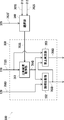
- FIG. 2 shows an example of the configuration of the selection determination unit 330.
- the selection determination unit 330 includes a selection unit 340 and a determination unit 350.
- the selection unit 340 outputs the comparison result 761S output from the first comparator 311 of the comparison unit 310 and the second comparator 312 based on the logical value of the test signal 753S ′ sent from the waveform shaping unit 220 via the delay unit 320.
- One of the comparison results 762S to be selected is selected.
- the selection unit 340 determines which logical value of the test signal 753S is superimposed on the superimposed signal 755S input to the comparison determination unit 300 based on the logical value for each bit of the test signal 753S ′, and The comparison result 761S or the comparison result 762S is selected according to the superposed logical value. More specifically, the selection unit 340 selects the comparison result 761S when the logic value of the test signal 753S ′ is H logic, that is, when the driver 230 outputs the test signal 753S of H logic. The selection unit 340 selects the comparison result 762S when the logical value of the test signal 753S ′ is L logic, that is, when the driver 230 outputs the L logic test signal 753S.
- the selection unit 340 outputs each logical value selected from each of the comparison result 761S and the comparison result 762S to the determination unit 350 as a selection result signal 763S. Note that the selection unit 340 preferably selects either the comparison result 761S or the comparison result 762S at the timing of each cycle of the test signal 753S ′.
- the determination unit 350 includes a comparison result acquisition unit 351, a logical comparison unit 352, and a prohibition determination unit 353.
- the determination unit 350 determines pass / fail of the device under test 600 based on the comparison result selected by the selection unit 340.
- the comparison result acquisition unit 351 acquires the logical value of the selection result signal 763S from the selection unit 340 at the strobe timing specified by the timing signal 772S supplied from the timing generation unit 110. Then, the comparison result acquisition unit 351 outputs the acquired logical value to the logical comparison unit 352 and the prohibition determination unit 353 as a logical pattern 764D.
- the comparison result acquisition unit 351 may be a flip-flop or a latch, for example.
- the logical comparison unit 352 logically compares each logical value of the logical pattern 764D input from the comparison result acquisition unit 351 with each logical value of the expected value pattern 756D input from the pattern generation unit 120. Then, the logical comparison unit 352 generates a pass determination when the logical values match as a result of the logical comparison, and generates a fail determination when the logical values do not match. Further, the logic comparison unit 352 outputs the generated pass determination and fail determination to the prohibition determination unit 353 as a pass / fail determination result 765D. In this example, the logic comparison unit 352 may output the pass / fail judgment result 765D to another member (for example, a fail memory) of the test apparatus 10. Further, the logic comparison unit 352 may determine pass / fail of the device under test 600 based on the generated pass / fail determination result 765D, and may output the pass / fail determination result to the prohibition determination unit 353.
- the prohibition determination unit 353 detects the strobe timing when the comparison result acquisition unit 351 acquires the logical value of the selection result signal 763S based on the strobe timing specified by the timing signal 772S supplied from the timing generation unit 110. To do. Then, the prohibition determination unit 353 determines whether or not the strobe timing is included in the prohibition area determined according to the edge timing at which the logical value of the test signal 753S transitions from H logic to L logic or from L logic to H logic. Determine whether.
- the prohibition determination unit 353 further compares the logical value of the selection result signal 763S acquired according to the strobe timing and the logical comparison result in the logical comparison unit 352. An error flag 766D is generated in association with the pass / fail judgment result 765D.
- the prohibition determination unit 353 may output the error flag 766D to another member (for example, a fail memory) of the test apparatus 10. Further, when the pass / fail determination result for determining pass / fail of the device under test 600 is input from the logic comparison unit 352, the prohibition determination unit 353 may generate the error flag 766D in association with the pass / fail determination result.
- FIG. 3 is a timing chart showing an example of a test of the device under test 600 by the test apparatus 10.
- a data string and a waveform with a symbol on the left side correspond to the data string and the waveform of each signal of the above-described pattern with the corresponding symbol, respectively.
- specific 10 cycles at the time of testing the device under test 600 are extracted and indicated as C1 to C10.
- the driver 230 causes the test signal 753S corresponding to each logical value of the test pattern 752D to be received. Is output to the device under test 600. On the other hand, the device under test 600 outputs a response signal 754S having a waveform corresponding to the logical value of “LHHLHLLHLH” in each cycle of C1 to C10.
- the propagation delay time until the response signal 754S output from the device under test 600 propagates on the transmission line 40 and is input to the comparison unit 310 of the comparison determination unit 300 is exactly one cycle. It shall be equivalent to Further, it is assumed that the propagation delay time until the test signal 753S output from the driver 230 is input to the comparison unit 310 of the comparison determination unit 300 can be ignored.
- the logic value of “LLHHLHLLHL” (the logic value “LHHLHLLHLH” of the response signal 754S output from the device under test 600 is delayed by one cycle in each cycle of C1 to C10.
- the response signal 754S having a waveform corresponding to (value) and the test signal 753S having a waveform corresponding to the logic value of “LHLHHLHL” are input.
- the first comparator 311 of the comparison unit 310 outputs a comparison result 761S obtained by comparing the voltage level of each cycle signal in the superimposed signal 755S with voltage levels (VOH1, VOL1) of a predetermined magnitude to the selection determination unit 330. .
- the first comparator 311 outputs a comparison result 761S having a waveform corresponding to the logical value of “LLLLHLLLHL” to the selection determination unit 330 in each cycle of C1 to C10.
- the voltage levels (VOH1, VOL1) are set to levels for determining the logical value of the response signal 754S from the superimposed signal 755S when the H logic of the test signal 753S is superimposed on the superimposed signal 755S, for example.
- the second comparator 312 of the comparison unit 310 provides the selection determination unit 330 with a comparison result 762S obtained by comparing the voltage level of the signal of each cycle in the superimposed signal 755S with the voltage level (VOH2, VOL2) having a predetermined magnitude. Output.
- the second comparator 312 outputs the comparison result 762S having a waveform corresponding to the logical value of “LHHHHHHLHL” to the selection determination unit 330 in each cycle of C1 to C10.
- the voltage levels (VOH2, VOL2) are set to levels for determining the logical value of the response signal 754S from the superimposed signal 755S when the L logic of the test signal 753S is superimposed on the superimposed signal 755S, for example.
- the selection unit 340 of the selection determination unit 330 for example, in each cycle of C1 to C10, when the logical value of the test signal 753S ′ supplied from the waveform shaping unit 220 via the delay unit 320 is H logic, that is, in this example Then, the comparison result 761S is selected in C2, C4, C5, C7, and C9.
- the selection unit 340 of the selection determination unit 330 performs comparison results in C1, C3, C6, C8, and C10 when the logical value of the test signal 753S ′ is L logic in each cycle of C1 to C10, that is, in this example. 762S is selected.
- the selection determination unit 330 selects the comparison result 761S or the comparison result 762S according to the logical value of the test signal 753S ′ having the same logical pattern as the logical pattern of the test signal 753S.
- the voltage level obtained by canceling the voltage level of the test signal 753S included in the signal 755S, that is, the logical value corresponding to the voltage level of the response signal 754S can be output to the comparison result acquisition unit 351 of the determination unit 350 as the selection result signal 763S. .
- the selection unit 340 outputs a selection result signal 763S having a logical value of “LLHHLHLLHL” to the comparison result acquisition unit 351 of the determination unit 350 in each cycle of C1 to C10.
- the comparison result acquisition unit 351 detects the logical value of the selection result signal 763S from the selection unit 340 at the strobe timing specified by the timing signal 772S supplied from the timing generation unit 110. Then, the comparison result acquisition unit 351 acquires the detected logical value.
- the comparison result acquisition unit 351 outputs the acquired logical value to the logical comparison unit 352 and the prohibition determination unit 353 as a logical pattern 764D having a logical value of “LLHHLHLLLHL” in each cycle of C1 to C10.
- the logical comparison unit 352 logically compares each logical value of the logical pattern 764D input from the comparison result acquisition unit 351 with each logical value of the expected value pattern 756D input from the pattern generation unit 120.
- the expected value pattern 756D input to the logic comparison unit 352 has a logic value of “LLHHLHLLLHL” in each cycle of C1 to C10.
- the logical comparison unit 352 generates a path determination on the assumption that the logical values coincide in each of the cycles C1 to C10 as a result of the logical comparison, and outputs the path determination result 765D to the prohibition determination unit 353.
- the operation of the prohibition determination unit 353 is the same as described above, and a description thereof is omitted.
- the test apparatus 10 cancels the component of the test signal 753S in the signal. Since the logical value of the response signal 754S can be compared with the logical value of the expected value pattern, the response signal 754S output from the device under test 600 can be accurately detected by the comparison / determination unit 300. Therefore, the quality determination of the device under test 600 can be performed more accurately.
- the comparison determination unit 300 can accurately detect the response signal 754S even when the test signal 753S output from the signal supply unit 200 is detected by the comparison determination unit 300, so-called I / O. Tests can be conducted without considering the effects of deadband. Therefore, the test apparatus 10 can perform the test of the device under test 600 more efficiently.
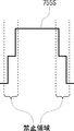
- FIG. 4 is an enlarged view of the signal waveform of the superimposed signal 755S in cycle C9.
- the prohibition determination unit 353 causes the comparison result acquisition unit 351 to select the logic of the selection result signal 763S. It is determined whether or not the strobe timing specified by the timing signal 772S when the value is acquired is included in the prohibited area shown in FIG.
- the prohibition determination unit 353 prevents the device under test 600 from being determined to be good or bad based on the result of the comparison result acquisition unit 351 acquiring the logical value of the selection result signal 763S at an inappropriate strobe timing. Can do. Further, the fact that the timing signal 751S is output at an inappropriate timing can be output as an error flag 766D.
- FIG. 5 shows another example of the configuration of the selection determination unit 330.
- the selection determination unit 330 according to this modification includes a determination unit 360 and a selection unit 370.
- the determination unit 360 includes comparison result acquisition units 361 and 362, logical comparison units 363 and 364, and a prohibition determination unit 365.
- the selection determination unit 330 outputs a determination result for determining whether the response signal 754S in each cycle is good or bad based on each of the comparison result 761S from the first comparator 311 and the comparison result 762S from the second comparator 312.
- the comparison result acquisition unit 361 detects the logical value of the comparison result 761S from the first comparator 311 at the strobe timing specified by the timing signal 772S supplied from the timing generation unit 110. Then, the comparison result acquisition unit 361 acquires the detected logical value and outputs it to the logical comparison unit 363 as a logical pattern 771D.
- the comparison result acquisition unit 362 detects the logical value of the comparison result 762S from the second comparator 312 at the strobe timing specified by the timing signal 772S supplied from the timing generation unit 110. Then, the comparison result acquisition unit 362 acquires the detected logical value and outputs it to the logical comparison unit 364 as a logical pattern 772D.
- the logical comparison unit 363 logically compares each logical value of the logical pattern 771D input from the comparison result acquisition unit 361 with each logical value of the expected value pattern 756D input from the pattern generation unit 120. Then, the logical comparison unit 363 generates a pass determination when the logical values match as a result of the logical comparison, and generates a fail determination when the logical values do not match. Then, the logical comparison unit 363 outputs the generated pass determination and fail determination to the selection unit 370 as a pass / fail determination result 773D.
- the logical comparison unit 364 logically compares each logical value of the logical pattern 772D input from the comparison result acquisition unit 362 with each logical value of the expected value pattern 756D input from the pattern generation unit 120. Then, the logical comparison unit 364 generates a pass determination when the logical values match as a result of the logical comparison, and generates a fail determination when the logical values do not match. Then, the logical comparison unit 364 outputs the generated pass determination and fail determination to the selection unit 370 as a pass / fail determination result 774D.
- the selection unit 370 determines which logical value of the test signal 753S is superimposed on the superimposed signal 755S input to the comparison determination unit 300, and performs the superimposition.
- the pass / fail judgment result 773D or the pass / fail judgment result 774D is selected according to the logical value.
- the selection unit 370 outputs the selection result signal 775S, which is a determination result selected from each of the pass / fail determination result 773D and the pass / fail determination result 774D, to the prohibition determination unit 365 of the determination unit 360.
- the operation of the prohibition determination unit 365 is substantially the same as that of the prohibition determination unit 353 and will not be described.
- the test apparatus 10 including the selection determination unit 330 including the determination unit 360 and the selection unit 370 described above is compared and determined similarly to the test apparatus 10 including the selection determination unit 330 including the selection unit 340 and the determination unit 350 described above. Even when the response signal 754S and the test signal 753S are superimposed in the unit 300, the component of the test signal 753S in the signal is canceled and the logical value of the response signal 754S is compared with the logical value of the expected value pattern 756D. Therefore, the comparison / determination unit 300 can accurately detect the response signal 754S output from the device under test 600. Therefore, the quality determination of the device under test 600 can be performed more accurately.
- the comparison determination unit 300 can accurately detect the response signal 754S even when the test signal 753S output from the signal supply unit 200 is detected by the comparison determination unit 300.
- the test can be carried out without considering the influence of the so-called I / O dead band. Therefore, the test apparatus 10 of the present example can perform the test of the device under test 600 more efficiently.
- the comparison unit 310 of the comparison determination unit 300 may include three or more comparators according to the number of voltage levels in the input superimposed signal 755S. For example, when the driver 230 does not output the H logic and the L logic, the impedance becomes high impedance, and the device under test has a predetermined voltage level different from the voltage level corresponding to the H logic and the voltage level corresponding to the L logic, for example.
- the comparison unit 310 of the comparison determination unit 300 may further include a comparator that detects the voltage at the time of the high impedance.
- the comparison unit 310 of the determination unit 300 may further include a comparator that detects the reference voltage.
- the comparator 312 may be configured to acquire a logical value of the ternary response signal as a multi-value measuring unit.
Landscapes
- Engineering & Computer Science (AREA)
- General Engineering & Computer Science (AREA)
- Physics & Mathematics (AREA)
- General Physics & Mathematics (AREA)
- Tests Of Electronic Circuits (AREA)
Abstract
Description
1.特願2008-13171 出願日 2008年1月23日
Claims (11)
- 被試験デバイスを試験する試験装置であって、
伝送路を介して前記被試験デバイスに試験信号を供給する信号供給部と、
前記信号供給部と共通の前記伝送路を介して前記被試験デバイスの応答信号を受け取り、前記試験信号の論理パターンに応じた参照レベルと前記応答信号の信号レベルとを比較した比較結果に基づいて、前記被試験デバイスの良否を判定する比較判定部と
を備える試験装置。 - 前記比較判定部は、
第1の参照レベルと前記応答信号の信号レベルとを比較した第1の比較結果を出力する第1コンパレータと、
前記第1の参照レベルとは異なる第2の参照レベルと前記応答信号の信号レベルとを比較した第2の比較結果を出力する第2コンパレータと、
前記第1の比較結果および前記第2の比較結果のうち、前記試験信号の論理パターンに応じた比較結果に基づいて、前記被試験デバイスの良否を判定する選択判定部と
を有する請求項1に記載の試験装置。 - 前記選択判定部は、
前記試験信号の論理パターンに基づいて、前記第1の比較結果および前記第2の比較結果のいずれかを選択する選択部と、
前記選択部が選択した比較結果に基づいて、前記被試験デバイスの良否を判定する判定部と
を含む請求項2に記載の試験装置。 - 前記試験信号の論理パターンを生成して前記信号供給部に供給するパターン発生部と、
前記パターン発生部が生成した前記試験信号の論理パターンを遅延させて前記選択部に供給する遅延部と
を更に備える請求項3に記載の試験装置。 - 前記判定部は、
予め定められたストローブタイミングで、前記比較結果の論理値を取得する比較結果取得部と、
前記比較結果取得部が取得した前記比較結果の論理値と、与えられる期待値とを論理比較する論理比較部と、
前記比較結果取得部における前記ストローブタイミングが、前記試験信号の論理値が遷移するエッジタイミングに応じて定められる禁止領域に含まれるか否かを判定する禁止判定部と
を含む請求項4に記載の試験装置。 - 前記禁止判定部は、前記ストローブタイミングが前記禁止領域に含まれる場合に、当該ストローブタイミングに応じて取得された前記論理値と、前記論理比較部における論理比較の結果に対応付けてエラーフラグを生成する
請求項5に記載の試験装置。 - 前記信号供給部は、H論理およびL論理のいずれかを出力するドライバを含み、
前記選択部は、前記ドライバがH論理およびL論理のいずれを出力しているかに応じて、前記第1の比較結果および前記第2の比較結果を選択する
請求項4から6の何れかに記載の試験装置。 - 前記第1の参照レベルは、前記第2の参照レベルより高く、
前記選択部は、前記ドライバがH論理を出力している場合に前記第1の比較結果を選択し、前記ドライバがL論理を出力している場合に前記第2の比較結果を選択する
請求項7に記載の試験装置。 - 前記比較判定部は、前記第1の参照レベルおよび前記第2の参照レベルとは異なる第3の参照レベルと前記応答信号の信号レベルとを比較した第3の比較結果を出力する第3コンパレータを更に有し、
前記選択部は、前記ドライバの出力がハイインピーダンスとなっている場合に、前記第3の比較結果を選択する
請求項8に記載の試験装置。 - 前記選択判定部は、
前記第1の比較結果および前記第2の比較結果のそれぞれに基づいて、前記被試験デバイスの良否をそれぞれ判定した判定結果を出力する判定部と、
前記試験信号の論理パターンに基づいて、前記第1の比較結果に対する第1の前記判定結果と、前記第2の比較結果に対する第2の前記判定結果のいずれかを選択する選択部と
を含む請求項2に記載の試験装置。 - 前記第1の比較結果および前記第2の比較結果に基づいて、多値の前記応答信号の論理値を取得する多値測定部を更に備える
請求項2に記載の試験装置。
Priority Applications (3)
| Application Number | Priority Date | Filing Date | Title |
|---|---|---|---|
| KR1020107015742A KR101138196B1 (ko) | 2008-01-23 | 2008-12-10 | 시험 장치 |
| JP2009550381A JP5226014B2 (ja) | 2008-01-23 | 2008-12-10 | 試験装置 |
| US12/838,428 US8427188B2 (en) | 2008-01-23 | 2010-07-16 | Test apparatus |
Applications Claiming Priority (2)
| Application Number | Priority Date | Filing Date | Title |
|---|---|---|---|
| JP2008013171 | 2008-01-23 | ||
| JP2008-013171 | 2008-01-23 |
Related Child Applications (1)
| Application Number | Title | Priority Date | Filing Date |
|---|---|---|---|
| US12/838,428 Continuation US8427188B2 (en) | 2008-01-23 | 2010-07-16 | Test apparatus |
Publications (1)
| Publication Number | Publication Date |
|---|---|
| WO2009093293A1 true WO2009093293A1 (ja) | 2009-07-30 |
Family
ID=40900814
Family Applications (1)
| Application Number | Title | Priority Date | Filing Date |
|---|---|---|---|
| PCT/JP2008/003702 Ceased WO2009093293A1 (ja) | 2008-01-23 | 2008-12-10 | 試験装置 |
Country Status (5)
| Country | Link |
|---|---|
| US (1) | US8427188B2 (ja) |
| JP (1) | JP5226014B2 (ja) |
| KR (1) | KR101138196B1 (ja) |
| TW (1) | TWI398648B (ja) |
| WO (1) | WO2009093293A1 (ja) |
Families Citing this family (4)
| Publication number | Priority date | Publication date | Assignee | Title |
|---|---|---|---|---|
| US8067943B2 (en) * | 2009-03-24 | 2011-11-29 | Advantest Corporation | Test apparatus, calibration method, program, and recording medium |
| US8855178B2 (en) * | 2011-03-02 | 2014-10-07 | Mediatek Inc. | Signal transmitter and signal transmitting method for transmitting specific data bit with different predetermined voltage levels |
| JP2014109453A (ja) * | 2012-11-30 | 2014-06-12 | Renesas Electronics Corp | 半導体装置 |
| US20150058042A1 (en) * | 2013-08-09 | 2015-02-26 | Aet, Llc | Consolidated patient information exchange |
Citations (2)
| Publication number | Priority date | Publication date | Assignee | Title |
|---|---|---|---|---|
| JP2002507754A (ja) * | 1998-03-26 | 2002-03-12 | テラダイン・インコーポレーテッド | 自動試験装置における往復遅延効果の補償 |
| JP2006023233A (ja) * | 2004-07-09 | 2006-01-26 | Advantest Corp | 半導体試験装置および半導体試験方法 |
Family Cites Families (11)
| Publication number | Priority date | Publication date | Assignee | Title |
|---|---|---|---|---|
| JP2627751B2 (ja) * | 1987-09-28 | 1997-07-09 | 株式会社アドバンテスト | Icテストシステム |
| JP3605146B2 (ja) | 1994-07-15 | 2004-12-22 | 株式会社アドバンテスト | I/oピンエレクトロニクス回路 |
| JP3509943B2 (ja) | 1994-07-20 | 2004-03-22 | 株式会社アドバンテスト | 伝送経路の伝播遅延時間測定回路 |
| US6469493B1 (en) * | 1995-08-01 | 2002-10-22 | Teradyne, Inc. | Low cost CMOS tester with edge rate compensation |
| JPH10253707A (ja) * | 1997-03-06 | 1998-09-25 | Ando Electric Co Ltd | 集積回路試験装置 |
| KR100299716B1 (ko) * | 1997-07-24 | 2001-09-06 | 가야시마 고조 | Ic시험장치및방법 |
| DE19980453T1 (de) * | 1998-02-09 | 2000-03-30 | Advantest Corp | Halbleiterbauelement-Testgerät |
| US6856158B2 (en) * | 2002-05-01 | 2005-02-15 | Advantest Corp. | Comparator circuit for semiconductor test system |
| JP4429625B2 (ja) * | 2003-04-25 | 2010-03-10 | 株式会社アドバンテスト | 測定装置、及びプログラム |
| JP4511880B2 (ja) | 2004-06-17 | 2010-07-28 | 株式会社アドバンテスト | 試験装置及び試験方法 |
| JP2007010606A (ja) * | 2005-07-04 | 2007-01-18 | Matsushita Electric Ind Co Ltd | Lsi検査モジュール、lsi検査モジュールの制御方法、lsi検査モジュールとlsi検査装置との通信方法、およびlsi検査方法 |
-
2008
- 2008-12-10 JP JP2009550381A patent/JP5226014B2/ja not_active Expired - Fee Related
- 2008-12-10 KR KR1020107015742A patent/KR101138196B1/ko active Active
- 2008-12-10 WO PCT/JP2008/003702 patent/WO2009093293A1/ja not_active Ceased
- 2008-12-30 TW TW097151405A patent/TWI398648B/zh active
-
2010
- 2010-07-16 US US12/838,428 patent/US8427188B2/en not_active Expired - Fee Related
Patent Citations (2)
| Publication number | Priority date | Publication date | Assignee | Title |
|---|---|---|---|---|
| JP2002507754A (ja) * | 1998-03-26 | 2002-03-12 | テラダイン・インコーポレーテッド | 自動試験装置における往復遅延効果の補償 |
| JP2006023233A (ja) * | 2004-07-09 | 2006-01-26 | Advantest Corp | 半導体試験装置および半導体試験方法 |
Also Published As
| Publication number | Publication date |
|---|---|
| TWI398648B (zh) | 2013-06-11 |
| JPWO2009093293A1 (ja) | 2011-05-26 |
| TW200933175A (en) | 2009-08-01 |
| US20110012612A1 (en) | 2011-01-20 |
| US8427188B2 (en) | 2013-04-23 |
| JP5226014B2 (ja) | 2013-07-03 |
| KR101138196B1 (ko) | 2012-05-14 |
| KR20100103602A (ko) | 2010-09-27 |
Similar Documents
| Publication | Publication Date | Title |
|---|---|---|
| US7725793B2 (en) | Pattern generation for test apparatus and electronic device | |
| US8719650B2 (en) | Self-diagnosis system and test circuit determination method | |
| JP5226014B2 (ja) | 試験装置 | |
| JP2010038581A (ja) | 半導体試験装置 | |
| US20090212818A1 (en) | Integrated circuit design method for improved testability | |
| US7973550B2 (en) | Semiconductor device test apparatus including interface unit and method of testing semiconductor device using the same | |
| JP5193975B2 (ja) | 半導体試験回路、半導体試験用冶具、半導体試験装置及び半導体試験方法 | |
| US20020178409A1 (en) | Method and apparatus for calibrating a test system for an integrated semiconductor circuit | |
| US8395406B2 (en) | Integrated circuit architecture for testing variable delay circuit | |
| US7240263B2 (en) | Apparatus for performing stuck fault testings within an integrated circuit | |
| WO2009150819A1 (ja) | 試験モジュール、試験装置および試験方法 | |
| US8055467B2 (en) | Method of generating a restricted inline resistive fault pattern and a test pattern generator | |
| JP2006012253A (ja) | 試験装置及び試験方法 | |
| US20110221488A1 (en) | Interface circuit with damping resistor circuit | |
| WO2009122699A1 (ja) | 試験モジュール、試験装置および試験方法 | |
| EP2704151A2 (en) | Semiconductor device and memory test method | |
| JP3818087B2 (ja) | 半導体集積回路装置 | |
| TW200907385A (en) | Test apparatus, test method, and manufacturing method of a device | |
| JP2006030079A (ja) | Lsiテスト装置およびlsiテスト方法 | |
| WO2010087009A1 (ja) | 電子デバイス、試験装置および試験方法 | |
| JP2006064607A (ja) | Icテスタ | |
| JP2004053411A (ja) | Icテスタ及びicのテスト方法 | |
| JP2010054402A (ja) | 回路試験装置、回路試験プログラムおよび回路試験方法 | |
| JP2005326203A (ja) | 半導体集積回路の実速度検査方法 | |
| JP2008256649A (ja) | 半導体試験装置 |
Legal Events
| Date | Code | Title | Description |
|---|---|---|---|
| 121 | Ep: the epo has been informed by wipo that ep was designated in this application |
Ref document number: 08871604 Country of ref document: EP Kind code of ref document: A1 |
|
| WWE | Wipo information: entry into national phase |
Ref document number: 2009550381 Country of ref document: JP |
|
| ENP | Entry into the national phase |
Ref document number: 20107015742 Country of ref document: KR Kind code of ref document: A |
|
| NENP | Non-entry into the national phase |
Ref country code: DE |
|
| 122 | Ep: pct application non-entry in european phase |
Ref document number: 08871604 Country of ref document: EP Kind code of ref document: A1 |