WO2009081769A1 - 回路基板の熱対策構造 - Google Patents
回路基板の熱対策構造 Download PDFInfo
- Publication number
- WO2009081769A1 WO2009081769A1 PCT/JP2008/072660 JP2008072660W WO2009081769A1 WO 2009081769 A1 WO2009081769 A1 WO 2009081769A1 JP 2008072660 W JP2008072660 W JP 2008072660W WO 2009081769 A1 WO2009081769 A1 WO 2009081769A1
- Authority
- WO
- WIPO (PCT)
- Prior art keywords
- circuit board
- terminal
- heat
- bus bar
- metal core
- Prior art date
Links
- 229910052751 metal Inorganic materials 0.000 claims abstract description 75
- 239000002184 metal Substances 0.000 claims abstract description 75
- 239000002344 surface layer Substances 0.000 claims abstract description 7
- 239000011347 resin Substances 0.000 claims description 13
- 229920005989 resin Polymers 0.000 claims description 13
- 239000000463 material Substances 0.000 claims description 10
- 239000010410 layer Substances 0.000 claims description 7
- 238000010276 construction Methods 0.000 claims 1
- 238000002791 soaking Methods 0.000 abstract description 3
- 238000010438 heat treatment Methods 0.000 description 10
- 230000017525 heat dissipation Effects 0.000 description 9
- 229910000679 solder Inorganic materials 0.000 description 8
- 238000010521 absorption reaction Methods 0.000 description 5
- 230000005855 radiation Effects 0.000 description 5
- 239000000758 substrate Substances 0.000 description 4
- RYGMFSIKBFXOCR-UHFFFAOYSA-N Copper Chemical compound [Cu] RYGMFSIKBFXOCR-UHFFFAOYSA-N 0.000 description 3
- 238000005452 bending Methods 0.000 description 3
- 229910052802 copper Inorganic materials 0.000 description 3
- 239000010949 copper Substances 0.000 description 3
- 229910052782 aluminium Inorganic materials 0.000 description 1
- XAGFODPZIPBFFR-UHFFFAOYSA-N aluminium Chemical compound [Al] XAGFODPZIPBFFR-UHFFFAOYSA-N 0.000 description 1
- 239000003795 chemical substances by application Substances 0.000 description 1
- 230000000694 effects Effects 0.000 description 1
- 239000000945 filler Substances 0.000 description 1
- 238000002156 mixing Methods 0.000 description 1
- 238000000465 moulding Methods 0.000 description 1
- 230000002093 peripheral effect Effects 0.000 description 1
- 239000011295 pitch Substances 0.000 description 1
- 229910052709 silver Inorganic materials 0.000 description 1
- 239000004332 silver Substances 0.000 description 1
- 229910052718 tin Inorganic materials 0.000 description 1
Images


Classifications
-
- H—ELECTRICITY
- H05—ELECTRIC TECHNIQUES NOT OTHERWISE PROVIDED FOR
- H05K—PRINTED CIRCUITS; CASINGS OR CONSTRUCTIONAL DETAILS OF ELECTRIC APPARATUS; MANUFACTURE OF ASSEMBLAGES OF ELECTRICAL COMPONENTS
- H05K1/00—Printed circuits
- H05K1/02—Details
- H05K1/0201—Thermal arrangements, e.g. for cooling, heating or preventing overheating
- H05K1/0203—Cooling of mounted components
- H05K1/0204—Cooling of mounted components using means for thermal conduction connection in the thickness direction of the substrate
- H05K1/0206—Cooling of mounted components using means for thermal conduction connection in the thickness direction of the substrate by printed thermal vias
-
- H—ELECTRICITY
- H05—ELECTRIC TECHNIQUES NOT OTHERWISE PROVIDED FOR
- H05K—PRINTED CIRCUITS; CASINGS OR CONSTRUCTIONAL DETAILS OF ELECTRIC APPARATUS; MANUFACTURE OF ASSEMBLAGES OF ELECTRICAL COMPONENTS
- H05K1/00—Printed circuits
- H05K1/02—Details
- H05K1/0201—Thermal arrangements, e.g. for cooling, heating or preventing overheating
-
- H—ELECTRICITY
- H05—ELECTRIC TECHNIQUES NOT OTHERWISE PROVIDED FOR
- H05K—PRINTED CIRCUITS; CASINGS OR CONSTRUCTIONAL DETAILS OF ELECTRIC APPARATUS; MANUFACTURE OF ASSEMBLAGES OF ELECTRICAL COMPONENTS
- H05K1/00—Printed circuits
- H05K1/02—Details
- H05K1/0213—Electrical arrangements not otherwise provided for
- H05K1/0263—High current adaptations, e.g. printed high current conductors or using auxiliary non-printed means; Fine and coarse circuit patterns on one circuit board
-
- H—ELECTRICITY
- H05—ELECTRIC TECHNIQUES NOT OTHERWISE PROVIDED FOR
- H05K—PRINTED CIRCUITS; CASINGS OR CONSTRUCTIONAL DETAILS OF ELECTRIC APPARATUS; MANUFACTURE OF ASSEMBLAGES OF ELECTRICAL COMPONENTS
- H05K7/00—Constructional details common to different types of electric apparatus
- H05K7/20—Modifications to facilitate cooling, ventilating, or heating
- H05K7/2039—Modifications to facilitate cooling, ventilating, or heating characterised by the heat transfer by conduction from the heat generating element to a dissipating body
- H05K7/205—Heat-dissipating body thermally connected to heat generating element via thermal paths through printed circuit board [PCB]
-
- H—ELECTRICITY
- H05—ELECTRIC TECHNIQUES NOT OTHERWISE PROVIDED FOR
- H05K—PRINTED CIRCUITS; CASINGS OR CONSTRUCTIONAL DETAILS OF ELECTRIC APPARATUS; MANUFACTURE OF ASSEMBLAGES OF ELECTRICAL COMPONENTS
- H05K1/00—Printed circuits
- H05K1/02—Details
- H05K1/0201—Thermal arrangements, e.g. for cooling, heating or preventing overheating
- H05K1/0203—Cooling of mounted components
-
- H—ELECTRICITY
- H05—ELECTRIC TECHNIQUES NOT OTHERWISE PROVIDED FOR
- H05K—PRINTED CIRCUITS; CASINGS OR CONSTRUCTIONAL DETAILS OF ELECTRIC APPARATUS; MANUFACTURE OF ASSEMBLAGES OF ELECTRICAL COMPONENTS
- H05K1/00—Printed circuits
- H05K1/02—Details
- H05K1/03—Use of materials for the substrate
- H05K1/05—Insulated conductive substrates, e.g. insulated metal substrate
-
- H—ELECTRICITY
- H05—ELECTRIC TECHNIQUES NOT OTHERWISE PROVIDED FOR
- H05K—PRINTED CIRCUITS; CASINGS OR CONSTRUCTIONAL DETAILS OF ELECTRIC APPARATUS; MANUFACTURE OF ASSEMBLAGES OF ELECTRICAL COMPONENTS
- H05K2201/00—Indexing scheme relating to printed circuits covered by H05K1/00
- H05K2201/10—Details of components or other objects attached to or integrated in a printed circuit board
- H05K2201/10227—Other objects, e.g. metallic pieces
- H05K2201/10272—Busbars, i.e. thick metal bars mounted on the printed circuit board [PCB] as high-current conductors
-
- H—ELECTRICITY
- H05—ELECTRIC TECHNIQUES NOT OTHERWISE PROVIDED FOR
- H05K—PRINTED CIRCUITS; CASINGS OR CONSTRUCTIONAL DETAILS OF ELECTRIC APPARATUS; MANUFACTURE OF ASSEMBLAGES OF ELECTRICAL COMPONENTS
- H05K3/00—Apparatus or processes for manufacturing printed circuits
- H05K3/30—Assembling printed circuits with electric components, e.g. with resistor
- H05K3/306—Lead-in-hole components, e.g. affixing or retention before soldering, spacing means
Definitions
- the present invention relates to a circuit board heat countermeasure structure that absorbs heat of a circuit board from a metal core of an intermediate layer or a pattern circuit of a surface layer by a terminal or a bus bar to equalize the heat and dissipate the heat to the outside.
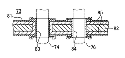
- the circuit board assembly 71 is mounted on a circuit board 73 having a printed circuit 81 (FIG. 9) and a flat copper metal core 82 (FIG. 9) in the thickness direction, and on the surface of the circuit board 73.
- the circuit board 73 includes a connector block 75 connected to both left and right sides of the circuit board 73 with terminals 74, and a fuse block 77 connected to the front of the circuit board 73 with terminals 76. is there.
- circuit board 73, the electrical / electronic component 72, and the blocks 75 and 77 are covered and protected by upper and lower covers (not shown) with the openings 75a and 77a of the blocks 75 and 77 exposed.
- Each of the component parts 72 to 77 including these covers constitutes a junction block.
- the electric and electronic components 72 connected to the circuit board include switching transistors 72 1 and the integrated circuit 72 2.
- the terminals 74 of the electric / electronic parts 72 and the connector block 75 are mainly soldered to the printed circuit 81 on the surface side of the circuit board 73, and some of the terminals 76 of the fuse block 77 are It is connected to the metal core 82 of the circuit board 73.
- reference numeral 85 denotes an insulating resin layer that sandwiches the metal core 82 from above and below
- reference numerals 83 and 84 denote through-holes into which the terminals 74 and 76 are inserted.
- the inner peripheral surfaces of the through holes 83 and 84 are covered with a conductive film, and the conductive film is connected to the printed circuit 81 and the metal core 82.
- the connector block 75 is a connector housing made of insulating resin (represented by reference numeral 75), one end side is inserted into the connector housing, and the other end side is inserted and soldered into the through hole 83 (FIG. 9) of the circuit board 73. And a plurality of parallel substantially L-shaped pin-like terminals 74.
- the fuse block 77 has an insulating resin fuse holder (block body) 78 and one end side inserted into the fuse holder 78, and the other end side inserted into the through hole 84 (FIG. 9) of the circuit board 73 and soldered.
- a connector 80 for power input that accommodates one side of the bus bar.
- a plurality of blade-type fuses (not shown) are mounted on the fuse holder 78 in two upper and lower stages and in parallel in the left-right direction, and a pair of upper and lower housings in the upper and lower housing chambers 77a corresponding to a pair of upper and lower terminals of the fuse.
- Each tuning fork terminal portion (clamping terminal) between the terminal 76 and the pair of upper and lower bus bars is inserted.
- the connector 80 receives battery power and alternator power.
- Patent Document 1 a separate terminal holder (not shown) is joined to the fuse holder 78, and each stage has an L-shaped terminal 76 (a terminal is used instead of the bus bar).
- L-shaped terminal 76 a terminal is used instead of the bus bar.
- Patent Document 2 describes that a mini-fuse and a medium-current fuse are mounted using a circuit board having a metal core with good heat dissipation, and Patent Document 3 faces a switching device on the circuit board.
- the conductive metal strip plate-like bus bar is arranged vertically on the circuit board, and heat generated by the switching device is absorbed by the bus bar to improve the heat dissipation of the power distribution unit.
- the metal core is formed of an aluminum plate instead of a copper plate.
- Japanese Patent Laying-Open No. 2006-335583 (FIGS. 6 and 1 to 2) JP 2006-42583 A (FIG. 1) JP 2006-187123 A (FIG. 5)
- the metal core 82 with good heat dissipation (uniform heat distribution) is used, depending on the type of the electric / electronic component 72 (for example, a relay or the like is used). In some cases, there is a concern that when the circuit board 73 is heated and deformed, or when the fuses are arranged in multiple stages, this heating may be promoted.
- the present invention can efficiently perform heat equalization and heat dissipation using a metal core, and can efficiently dissipate or heat heat from a heat-generating component, It is an object of the present invention to provide a circuit board heat countermeasure structure that can ensure heat equalization and heat dissipation of a circuit board even when electric parts such as fuses are arranged in a plurality of stages (multistage).
- a circuit board thermal countermeasure structure comprises a terminal block composed of an insulating block body and a plurality of terminals, and the circuit board is connected to at least one of the terminals.
- a plurality of terminal portions are formed, and the plurality of terminal portions are inserted into each through hole of a circuit board having a conductive metal core in the middle in the thickness direction, and the heat of the metal core is transferred to the terminal side at the plurality of terminal portions. It is characterized by absorbing heat.
- the heat of the circuit board is sucked up from the metal core by a plurality of terminal portions of the terminal and efficiently transferred to the terminals (terminal body excluding the terminal portions), so that the heat is soaked and dissipated.
- the heat of the terminal body is released by radiation or heat transfer to the block body.
- the plurality of terminal portions may be in direct contact with the inner surface of the through hole of the metal core, or may be in indirect contact via solder.
- the plurality of terminals have a terminal part for connecting a circuit board on one side and a terminal part for connecting an electrical component such as a fuse on the other side.
- the heat countermeasure structure for a circuit board according to claim 2 is the heat countermeasure structure for a circuit board according to claim 1, wherein a terminal portion for connecting an electric wire is provided on the at least one terminal, and the electric wire is connected to the electric wire from the terminal portion. It is characterized by heat being transmitted.
- the heat sucked from the circuit board by the terminal is continuously and efficiently transmitted to the external electric wire via the terminal portion for connecting the electric wire, and the heat of the electric wire is absorbed in the longitudinal direction of the electric wire or from the outer periphery of the electric wire. Radiation to the outside reliably prevents the temperature rise of the circuit board.
- a circuit board heat countermeasure structure comprising a bus bar block composed of an insulating block body and a plurality of parallel bus bars, the lengths of the plurality of bus bars being variously set, Each terminal portion on the front end side of the bus bar of various lengths is inserted into each through hole of a circuit board having a conductive metal core in the middle of the thickness direction, and the heat of the metal core or the pattern circuit is inserted at each terminal portion. The heat with the metal core is absorbed into the bus bar side.
- each bus bar has a terminal part for connecting a circuit board on one side and a terminal part for connecting an electrical component such as a fuse on the other side.
- the circuit board thermal countermeasure structure according to claim 4 comprises a bus bar block comprising an insulating block body and a plurality of parallel bus bars, and has a surface pattern circuit and a conductive metal core in the middle of the thickness direction.
- a plurality of exothermic components are mounted on the terminal, and a terminal portion on the front end side of the bus bar is inserted into a through hole of the circuit board in the vicinity of the exothermic component, and the heat of the metal core or the pattern is formed at the terminal portion. The heat of the circuit and the metal core is absorbed to the bus bar side.
- the terminal portion of the bus bar may be in direct contact with the inner surface of the through hole of the metal core or the inner surface of the through hole of the pattern circuit, or may be in indirect contact with the solder. It is also possible to connect the terminal portion to both the metal core and the pattern circuit within one through hole.
- Each bus bar has a terminal part for connecting a circuit board on one side and a terminal part for connecting an electrical component such as a fuse on the other side.
- the circuit board heat countermeasure structure according to claim 5 is the circuit board heat countermeasure structure according to claim 3 or 4, wherein a length to the tip of the bus bar is set longer than a length of the block main body. Projecting long from the block main body to the outside.
- the bus bar protrudes from the end of the block main body and is greatly exposed to the outside, so that the heat dissipation (radiation to the outside) of the bus bar is enhanced, and the heat of the metal core and pattern circuit from the bus bar terminal is increased. Sucking and soaking are performed efficiently.
- a circuit board thermal countermeasure structure according to claim 6 is the circuit board thermal countermeasure structure according to any one of claims 3 to 5, comprising the circuit board thermal countermeasure structure according to claim 1 or 2, wherein The terminal block is disposed on the surface of the circuit board, the bus bar block is disposed on the terminal block, and terminal portions for connecting electrical components between the terminal and the bus bar are disposed in a plurality of layers.
- a plurality of electrical components such as fuses are provided for each terminal portion for connecting electrical components of each terminal of the lower terminal block and each terminal portion for connecting electrical components of each bus bar of the upper bus bar block. It is arranged and connected in layers (multilayers). The heat of the metal core of the circuit board and the pattern circuit is efficiently sucked up by both the terminal and the bus bar.
- the circuit board thermal countermeasure structure according to claim 7 is the circuit board thermal countermeasure structure according to any one of claims 1 to 6, wherein the block main body is formed of a resin material having high thermal conductivity.
- the heat of the metal core and pattern circuit sucked up from the terminal part for connecting each circuit board of the terminal and bus bar is surely absorbed by each block main body having high thermal conductivity in the terminal block and bus bar block, and is released to the outside.
- the circuit board is absorbed by the terminals and the bus bar and heat is soaked continuously.
- the terminal can efficiently absorb the heat of the circuit board, thereby heating the circuit board (unnecessary temperature rise). ) Can be reliably prevented with a simple structure.
- the heat sucked up from the circuit board is transmitted from the terminal portion to the electric wire, so that the heat absorption by the terminal is continuously performed, and the heating of the circuit board is more reliably prevented.
- the metal core or the pattern circuit and the metal core are absorbed by the terminal portions of the plurality of bus bars in a wide range, the circuit board is efficiently heated and radiated, Is reliably prevented from being heated.
- the heat sucked up from the metal core or the pattern circuit is efficiently radiated by the bus bar itself, so that the heating of the circuit board is more reliably prevented.
- the heat of the metal core or the pattern circuit is reliably transmitted from the terminal or bus bar to the block main body and efficiently radiated from the block main body to the outside, so that the heat absorption of the circuit board by the terminal or bus bar is achieved. Is continuously performed, and heating of the circuit board is more reliably prevented.
- FIG. 1 is a perspective view showing a first embodiment of a circuit board heat countermeasure structure according to the present invention. It is a principal part perspective view similarly changing the angle which looks at 1st embodiment. It is a perspective view which shows 2nd embodiment of the heat countermeasure structure of the circuit board which concerns on this invention. It is a top view which similarly shows 2nd embodiment. It is the perspective view which looked at the bus-bar block in 2nd embodiment from the back surface side.
- the third embodiment of the circuit board thermal countermeasure structure according to the present invention is shown, (a) is a perspective view, (b) is a side view. It is a perspective view which shows one form of the circuit board assembly of a completion state. It is a perspective view which shows one form of the conventional circuit board assembly. It is a longitudinal cross-sectional view which shows one form of the conventional circuit board.
- Circuit board 3 Terminal block 4
- Bus bar block 7 Relay (heat-generating component) 13 block body 14, 14 'terminal 14a, 19a terminal part 14b terminal part 15 terminal part 16 each through hole 18 block body 19 bus bar 19b terminal part 82 metal core
- FIG. 1 and 2 show a first embodiment of a circuit board heat countermeasure structure according to the present invention.
- a terminal block 3 is disposed on a circuit board 2 having a conductive flat metal core (see reference numeral 82 in FIG. 9) in an intermediate portion in the board thickness direction, and the flat terminal (bus bar) of the terminal block 3 is arranged. ) 14, a plurality of pin-like terminal portions 14b are formed in parallel, and the plurality of terminal portions 14b are inserted into the respective through holes 16 of the circuit board 2 to form a conductive layer on the inner surface of the through hole 16 of the metal core. Solder connection was made in the state of contact (or contact was made with the conductive layer on the inner surface of the through hole 16 of the metal core via solder).
- FIG. 1 Since the basic configuration of the metal core is the same as that in FIG. 9 of the conventional example, detailed description will be omitted with reference to FIG. In FIG. 1, only the insulating substrate 2a covering the front and back of the metal core is shown.
- the metal core is arranged in the range of the length and width of the insulating substrate 2a.
- a printed circuit pattern circuit on the surface layer side (not shown) is formed in a required pattern on the front surface and / or back surface of the insulating substrate 2a.
- the terminal block 3 includes a block main body 13 made of insulating resin and a plurality of power terminals 14 and 14 ′ held by the block main body 13.
- the plurality of terminals 14 and 14 ' are configured by a wide flat-plate terminal (bus bar) 14 having an L-shaped vertical section shown in an enlarged view and a narrow terminal 14' having an L-shaped vertical section. .
- the narrow terminal 14 ' has about one or two pin-like terminal portions 14b.
- Each terminal 14, 14 ′ is composed of a horizontal portion 14 c parallel to the circuit board 2 and a vertical portion 14 d orthogonal to the circuit board 2, and the horizontal portion 14 c is formed in a tuning fork-like shape for fuse connection on the tip (front end) side.
- the sandwiching terminal portion 14a is integrally provided, and the vertical portion 14d is integrally provided with a pin-like terminal portion 14b for circuit board connection on the tip (lower end) side.
- a plurality (four in this example) of pin-like terminal portions 14b are formed in parallel with each other on the vertical plate portion 14d of the wide terminal 14, and the plurality of terminal portions 14b are formed on the circuit board 2 in parallel.
- a tab-shaped terminal portion 15 is integrally formed on the side of the horizontal plate portion 14c of the wide terminal 14, and is crimped to the tab-shaped terminal portion 15 on the distal end side of a large-diameter external electric wire (not shown).
- a large-diameter external electric wire not shown.
- the electric wire is connected to the battery side or alternator side of the vehicle.
- Each pin-shaped terminal portion 14b of the wide terminal 14 is formed short, and in this example, a vertically long slit 14e is formed in the vertical plate portion 14d at the center of the four pin-shaped terminal portions 14b, for a total of four pin-shaped terminals.
- the portion 14b is divided into left and right pairs.
- the slit 14e absorbs the thermal distortion of the vertical plate portion 14d when the solder is melted, and reduces the stress at the solder connection portion between each pin-like terminal portion 14b and the circuit board 2.
- a plurality of sandwiching terminal portions 14 a are formed in parallel at equal pitches on the horizontal plate portion 14 c of the wide terminal 14.
- the sandwiching terminal portion 14a is composed of a pair of left and right elastic contact pieces and a slit therebetween, and is connected by sandwiching one of a pair of upper and lower tab terminals of a small blade-type fuse (not shown).
- the tab terminal portion 15 projecting sideways is formed wide so as to correspond to a relatively large current.
- a narrow tab terminal portion 14f formed in parallel with the holding terminal portion 14a is for connecting a box-shaped fusible link (not shown).
- the terminal block 3 holds terminals 14 and 14 'in a plurality of stages (four stages in this example) in the vertical direction.
- the horizontal portion 14c of the wide terminal 4 is arranged at the uppermost stage.
- the fuses are arranged vertically in two stages.
- the block main body 13 includes a main body portion 13a and an upper cover portion 13b.
- the vertical portions 14d of the terminals 14 and 14 ′ are inserted into the main body portion 13a downward from above, and the cover portion 13b is connected to the terminals 14 and 14 ′.
- the vertical plate portion 14d of the wide terminal 14 is inserted into the wide concave portion 47 of the rear wall of the main body portion 13a of the block body 13, and each pin-like terminal portion 14b protrudes downward from the lower end of the concave portion 47, so that the main portion 13a While the bottom surfaces of the side walls 48 are in contact with the upper surface of the circuit board 2, the pin-like terminal portions 14 b are inserted into the through holes 16 of the circuit board 2 and soldered to the metal cores in the through holes.
- the number of pin-like terminal portions 14b is not limited to four, and the more the number of pin-like terminal portions 14b, the higher the heat absorption (heat absorption) property from the metal core of the circuit board 2.
- a fuse holder (not shown) made of an insulating resin is mounted on the front end side of the block main body 13, and each clamping terminal portion 14 a protruding forward from the block main body 13 is accommodated in the fuse holder, and each fuse is inserted into the fuse holder. Mounted horizontally from the front.
- a plurality of relays 7 are arranged and connected in parallel in the left-right direction and in the front-rear direction (the longitudinal direction of the board) in the center of the circuit board 2 in the width direction.
- the relay 7 is a heating element that generates a large amount of heat, and is a factor that increases the temperature of the circuit board 2.
- Small resistor components 49 are arranged and connected to the important points of the circuit board 2.
- the circuit board 2, terminal block 3, and electrical / electronic components such as the relay 7 constitute a circuit board assembly (subassembly) 12.
- the front / back / up / down / left / right directions are merely for convenience of explanation, and do not necessarily coincide with the mounting direction of the circuit board assembly 12.
- the block body 13 of the terminal block 3 is formed of a resin material having high thermal conductivity
- the heat sucked up by the terminals 14 and 14 ′ can be efficiently radiated from the block body 13 to the outside.
- the resin material having a high thermal conductivity a material formed by blending a filler such as a metal having a high thermal conductivity with a resin agent can be given. Since the bottom surfaces of the side walls 48 of the block body 13 are in contact with the surface of the circuit board 2, the heat on the front side of the circuit board 2 is also radiated from the block body 13.
- 3 to 5 show a second embodiment of the circuit board heat countermeasure structure according to the present invention.
- a bus bar block 4 is disposed on a circuit board 2 having a pattern circuit (printed circuit) on the surface layer and a conductive flat metal core (see reference numeral 82 in FIG. 9) in the middle in the board thickness direction.
- a plurality of parallel power bus bars 19 in the form of strips of the bus bar block 4 are formed by bending a short vertical portion 19f on the tip end side of each horizontal portion 19e parallel to the circuit board 2, and the tip of each vertical portion 19f.
- the pin-shaped terminal portion 19b on the (lower end) side is inserted into each through hole 16 of the circuit board 2 and is in contact with the inner surface of the through hole 16 of the metal core or the inner surface of the through hole 16 of the pattern circuit and the metal core. Solder-connected (or brought into contact with the inner surface of the through hole 16 of the metal core or the inner surface of the through hole 16 of the pattern circuit and the metal core via solder).
- the surface layer includes the front and back sides.
- the circuit board 2 is the same as that of the embodiment of FIG. 1, and the arrangement of components such as the relay 7 is the same.
- the through hole 16 into which the pin-shaped terminal portion 19b of the bus bar 19 is inserted is formed in an arbitrary portion of the circuit board 2 and is formed between the adjacent relays 7 at the front and rear.
- the bus bar block 4 includes a block main body 18 made of an insulating resin and a plurality of bus bars 19 and 19 ′ provided in parallel on both front and back (upper and lower) surfaces of the block main body 18.
- FIG. 5 shows the bus bar 19 'on the back side.
- Each bus bar 19, 19 ′ is preferably fixed to the block main body 18 by insert molding.
- the bus bar 19, 19 ′ is arranged in a routing groove (not shown) in the front-rear direction of the block main body 18, A small protrusion (not shown) integrated with 18 may be inserted into the small holes of the bus bars 19 and 19 ′ and fixed by heat caulking.
- 1 is formed on the front end (front end) side of each bus bar 19, 19 ′, and a fuse connection clamping terminal portion 19 a having the same shape as the terminal 14 of FIG. 1 is formed. 1 is formed with a pin-shaped terminal portion 19b for circuit board connection having the same shape as that of the terminal 14 in FIG.
- the upper and lower tab terminals of the fuse (not shown) are inserted and connected to the sandwiching terminal portions 19a of the upper and lower (front and back) bus bars 19 and 19 '.
- the upper bus bar 19 protrudes (exposes) long backward from the block main body 18, and the lower bus bar 19 ′ is routed in the longitudinal range of the block main body 18 as shown in FIG. 5.
- the block main body 18 is formed in a substantially crank-shaped stepped shape, and has a horizontal wall portion 20 on the upper front side, a horizontal wall portion 21 on the lower rear side, and a short intermediate connecting the wall portions 20 and 21. And a vertical wall portion 22.
- a horizontal wall portion 20 on the upper front side
- a horizontal wall portion 21 on the lower rear side
- a short intermediate connecting the wall portions 20 and 21 and a vertical wall portion 22.
- a vertical wall portion 22 For example, it is possible to extend the vertical wall portion 22 downward so as to contact and support the surface of the circuit board 2.
- Each bus bar 19, 19 ' is also formed in a step shape along the shape of the block body 18, and a front horizontal portion 19c, a rear horizontal portion 19e, and a short intermediate vertical portion 19d connecting the horizontal portions 19c, 19e. And a rear vertical portion 19f bent downward from the rear horizontal portion 19e.
- a clamping terminal portion 19a is integrally formed at the front end of the front horizontal portion 19c, and the rear vertical portion 19f
- a pin-like terminal portion 19b is integrally formed at the lower end.
- Each clamping terminal portion 19 a protrudes forward from the front end of the horizontal wall portion 20 on the upper side of the block body 18.
- a part (left end portion) of the lower horizontal wall portion 21 on the lower side of the block main body 18 is extended rearward, and the upper and lower bus bars 19, 19 ′ are extended while being insulated along the front and back surfaces of the extended wall portion 21a.
- the lower bus bar 19 ′ is formed short at the portion other than the extension portion 21 a, and the upper bus bar 19 is formed long in the front-rear direction over the entire width of the block body 18.
- the upper-level bus bar 19 is composed of a plurality of bus bar groups 191 to 196 having different lengths, a long bus bar group 191 at the right end, a second short bus bar group 192 from the right end, and a third longest bus bar group.
- the bus bar 19 in each of the bus bar groups 191 to 196 has two or three bus bars having a rear horizontal portion 19e and a rear vertical portion 19f having the same length (the bending position 19g of the vertical portion 19f is the same). 19.
- the metal cores of the circuit board 2 are connected to a part or all of the bus bar groups 191 to 196 in a wide range in the longitudinal direction of the circuit board 2.
- the heat is efficiently sucked (heat absorbed) by the bus bar groups 191 to 196 at a plurality of locations in the length direction and width direction of the metal core, so that the heat is soaked and radiated from the outer surface of each bus bar 19 to the outside.
- the remaining portions of the bus bar groups 191 to 196 except for a part thereof are connected to the pattern circuit on the surface layer of the circuit board 2.
- the heat of the circuit board 2 is efficiently sucked (heat absorbed) by the bus bar groups 191 to 196 at one place or a plurality of places in the pattern circuit, and is radiated from the outer surface of each bus bar 19 to the outside.
- the horizontal portion 19e passes above each relay 7 on the circuit board 2 and is located between the adjacent relays 7 (gap 50) and the relay 7 In the vicinity, the vertical portion 19 f is suspended toward the circuit board 2, and the pin-shaped terminal portions 19 b are inserted and connected to the through holes 16 of the circuit board 2.
- the block main body 18 of the bus bar block 4 is formed of a resin material having high thermal conductivity as in the terminal block 3 of the previous example, the heat sucked up by the bus bar 19 can be efficiently radiated from the block main body 18 to the outside. Can do.
- bus bar 19 with a material having higher conductivity is effective in improving heat dissipation.
- a material having high conductivity for example, a material obtained by adding silver or the like to copper, a material obtained by suppressing the addition amount of Sn or Mg, and the like can be given.
- FIG. 6 shows a third embodiment of the circuit board thermal countermeasure structure according to the present invention. This structure is configured by combining the embodiment of FIG. 1 and the embodiment of FIG.
- the terminal block 3 of FIG. 1 is arranged on the surface of the circuit board 2, and the bus bar block 4 of FIG. 3 is arranged on the terminal block 3.
- the lower surface of the horizontal wall portion 20 on the upper front side of the bus bar block main body 18 is supported on and supported by the upper cover 13b of the terminal block main body 13, and the terminal 14 and the bus bar 19 of each block 3 and 4 are in this state.
- the pin-like terminal portions 14b and 19b are inserted into the through holes 16 of the circuit board 2 and soldered.
- the pin-like terminal portions 14b and 19b of the terminal 14 and the bus bar 19 are in contact with the metal core or the pattern circuit and the metal core in a wide range of the circuit board 2, the heat of the circuit board 2, that is, the heat of the metal core or the pattern circuit is generated. It is sucked up uniformly and efficiently by the terminal 14 and the bus bar 19 and is soaked and radiated.
- the clamping terminal portions 14a and 19a between the terminal 14 and the bus bar 19 are arranged in multiple layers (six steps in this example) in the vertical direction, and a fuse holder (not shown) is attached to each block body 13 and 18 from the front.
- Each holding terminal portion 14a, 19a is accommodated in each accommodating chamber of the fuse holder, and a fuse (not shown) is mounted in each accommodating chamber from the front and arranged in three stages, and each clamping terminal is connected to each tab terminal of each fuse.
- the fuse blocks (power supply block) 5 are configured by inserting and connecting the portions 14a and 19a.
- the circuit board 2, the terminal block 3, and the bus bar block 4 constitute a circuit board assembly (subassembly) 17.
- FIG. 7 shows one form of the circuit board assembly 25 in a completed state in which the relay 7, the connector block 8, and the connector 11 are arranged and connected to the circuit board assembly 17 of FIG.
- the bus bar block 4 and the terminal block 3 are arranged on the front part of the circuit board 2 as a fuse block in a state where they are overlapped vertically, the connector block 8 is arranged on both the left and right sides of the circuit board 2, and the connector 11 for connecting the control unit is the rear
- the relay 7 is disposed inside the L-shaped terminal 26 that protrudes from the left and right connector blocks 8.
- the circuit board assembly 25 is covered with upper and lower insulating resin covers (not shown) to form a junction block.
- the fuse connection terminal 14 and the bus bar 19 are used, but it is also possible to use a fusible link, a relay, or the like in addition to the fuse as an electrical component.
- a fusible link, a relay, or the like in addition to the fuse as an electrical component.
- tab terminal portions or the like are formed on the terminals 14 and the bus bars 19 instead of the sandwiching terminal portions 14a and 19a.
- the plate-like tab terminal portion 15 is formed as the terminal portion for connecting the wire of the terminal 14, but a female terminal portion (not shown) is used instead of the tab terminal portion. It is also possible to form or connect a terminal-attached electric wire (not shown) with a bolt and a nut without using a connector connection.
- the bus bar block 4 is bent in a step shape (crank shape).
- the shape of the bus bar block 4 is not limited to this, and the bus bar block 4 is straight without bending in a step shape. It is also possible to arrange the block body (18) directly on the surface of the circuit board 2 by using the (planar) block body (18) and the bus bar (19).
- the circuit board is heated and deformed, and when the fuses are arranged in multiple stages, this heating is promoted. This problem can be solved by increasing the connection point of the terminal with respect to.
Landscapes
- Engineering & Computer Science (AREA)
- Microelectronics & Electronic Packaging (AREA)
- Physics & Mathematics (AREA)
- Thermal Sciences (AREA)
- Coupling Device And Connection With Printed Circuit (AREA)
- Insulated Metal Substrates For Printed Circuits (AREA)
- Cooling Or The Like Of Electrical Apparatus (AREA)
- Structure Of Printed Boards (AREA)
- Multi-Conductor Connections (AREA)
Abstract
Description
3 端子ブロック
4 バスバーブロック
7 リレー(発熱性の部品)
13 ブロック本体
14,14’ 端子
14a,19a 端子部
14b 端子部
15 端子部
16 各スルーホール
18 ブロック本体
19 バスバー
19b 端子部
82 メタルコア
Claims (7)
- 絶縁性のブロック本体と複数の端子とで端子ブロックを構成し、少なくとも一つの該端子に回路基板接続用の端子部を複数形成し、厚み方向中間に導電性のメタルコアを有する回路基板の各スルーホールに該複数の端子部を挿入し、該複数の端子部で該メタルコアの熱を該端子側に吸熱することを特徴とする回路基板の熱対策構造。
- 前記少なくとも一つの端子に電線接続用の端子部が設けられ、該端子部から該電線に前記熱が伝えられることを特徴とする請求項1記載の回路基板の熱対策構造。
- 絶縁性のブロック本体と複数の並列なバスバーとでバスバーブロックを構成し、該複数のバスバーの長さを種々に設定し、表層のパターン回路と厚み方向中間の導電性のメタルコアとを有する回路基板の各スルーホールに、該種々の長さのバスバーの先端側の各端子部を挿入し、各端子部で該メタルコアの熱又は該パターン回路と該メタルコアとの熱を該バスバー側に吸熱することを特徴とする回路基板の熱対策構造。
- 絶縁性のブロック本体と複数の並列なバスバーとでバスバーブロックを構成し、表層のパターン回路と厚み方向中間の導電性のメタルコアとを有する回路基板に発熱性の部品を複数実装すると共に、該発熱性の部品の近傍において、該バスバーの先端側の端子部を該回路基板のスルーホールに挿入し、該端子部で該メタルコアの熱又は該パターン回路と該メタルコアとの熱を該バスバー側に吸熱することを特徴とする回路基板の熱対策構造。
- 前記バスバーの先端までの長さが前記ブロック本体の長さよりも長く設定され、該バスバーが該ブロック本体から外部に長く突出していることを特徴とする請求項3又は4記載の回路基板の熱対策構造。
- 請求項1又は2記載の回路基板の熱対策構造を備える請求項3~5の何れかに記載の回路基板の熱対策構造であって、前記回路基板の表面上に前記端子ブロックを配置し、該端子ブロックの上に前記バスバーブロックを重ねて配置し、前記端子と前記バスバーとの電気部品接続用の端子部を複数層に配置したことを特徴とする回路基板の熱対策構造。
- 前記ブロック本体が熱伝導性の高い樹脂材で形成されたことを特徴とする請求項1~6の何れかに記載の回路基板の熱対策構造。
Priority Applications (6)
| Application Number | Priority Date | Filing Date | Title |
|---|---|---|---|
| EP08864352.3A EP2224798B1 (en) | 2007-12-21 | 2008-12-12 | Circuit board structure having measures against heat |
| US12/735,193 US8624122B2 (en) | 2007-12-21 | 2008-12-12 | Circuit board structure having measures against heat |
| CA2709793A CA2709793C (en) | 2007-12-21 | 2008-12-12 | Circuit board structure having measures against heat |
| CN200880126336.5A CN101940078B (zh) | 2007-12-21 | 2008-12-12 | 电路基板的热应对结构 |
| AU2008341972A AU2008341972B2 (en) | 2007-12-21 | 2008-12-12 | Circuit board structure having measures against heat |
| US14/091,901 US8867212B2 (en) | 2007-12-21 | 2013-11-27 | Circuit board structure having measures against heat |
Applications Claiming Priority (2)
| Application Number | Priority Date | Filing Date | Title |
|---|---|---|---|
| JP2007329993A JP5026947B2 (ja) | 2007-12-21 | 2007-12-21 | 回路基板の熱対策構造 |
| JP2007-329993 | 2007-12-21 |
Related Child Applications (2)
| Application Number | Title | Priority Date | Filing Date |
|---|---|---|---|
| US12/735,193 A-371-Of-International US8624122B2 (en) | 2007-12-21 | 2008-12-12 | Circuit board structure having measures against heat |
| US14/091,901 Division US8867212B2 (en) | 2007-12-21 | 2013-11-27 | Circuit board structure having measures against heat |
Publications (1)
| Publication Number | Publication Date |
|---|---|
| WO2009081769A1 true WO2009081769A1 (ja) | 2009-07-02 |
Family
ID=40801075
Family Applications (1)
| Application Number | Title | Priority Date | Filing Date |
|---|---|---|---|
| PCT/JP2008/072660 WO2009081769A1 (ja) | 2007-12-21 | 2008-12-12 | 回路基板の熱対策構造 |
Country Status (7)
| Country | Link |
|---|---|
| US (2) | US8624122B2 (ja) |
| EP (1) | EP2224798B1 (ja) |
| JP (1) | JP5026947B2 (ja) |
| CN (1) | CN101940078B (ja) |
| AU (1) | AU2008341972B2 (ja) |
| CA (1) | CA2709793C (ja) |
| WO (1) | WO2009081769A1 (ja) |
Cited By (1)
| Publication number | Priority date | Publication date | Assignee | Title |
|---|---|---|---|---|
| EP4033867A1 (de) * | 2020-12-18 | 2022-07-27 | LEONI Bordnetz-Systeme GmbH | Elektrische schaltvorrichtung |
Families Citing this family (22)
| Publication number | Priority date | Publication date | Assignee | Title |
|---|---|---|---|---|
| JP5179855B2 (ja) * | 2007-12-21 | 2013-04-10 | 矢崎総業株式会社 | バスバーブロックの組付構造 |
| JP5185608B2 (ja) * | 2007-12-21 | 2013-04-17 | 矢崎総業株式会社 | ジャンクションブロック |
| US8547684B2 (en) * | 2009-12-17 | 2013-10-01 | Schneider Electric USA, Inc. | Panelboard having a parallel feeder bars distribution |
| JP5307052B2 (ja) * | 2010-02-19 | 2013-10-02 | 古河電気工業株式会社 | 車載電気接続箱、及びこれに用いられる回路材、回路ユニット |
| JP5715766B2 (ja) * | 2010-04-22 | 2015-05-13 | 矢崎総業株式会社 | 配線材の接続構造 |
| CN102271459B (zh) * | 2010-06-03 | 2014-09-24 | 矢崎总业株式会社 | 布线基板及其制造方法 |
| JP5634823B2 (ja) | 2010-10-20 | 2014-12-03 | 矢崎総業株式会社 | メタルコア基板、それを備えた電気接続箱 |
| US9179560B2 (en) * | 2010-10-25 | 2015-11-03 | Korea Electric Terminal Co., Ltd. | Board block for vehicles |
| JP5723170B2 (ja) | 2011-02-04 | 2015-05-27 | 矢崎総業株式会社 | ヒューズ接続部品 |
| DE102011088256A1 (de) * | 2011-12-12 | 2013-06-13 | Zf Friedrichshafen Ag | Multilayer-Leiterplatte sowie Anordnung mit einer solchen |
| CN102608363B (zh) * | 2012-03-20 | 2015-11-11 | 常州亿晶光电科技有限公司 | 电致发光测试仪 |
| US9402320B2 (en) * | 2012-11-15 | 2016-07-26 | International Business Machines Corporation | Electronic component assembly |
| US9622355B2 (en) * | 2013-07-08 | 2017-04-11 | Delphi Technologies, Inc. | Environmentally sealed electrical housing assembly with integrated connector |
| US9532458B2 (en) * | 2014-11-17 | 2016-12-27 | Tyco Electronics Corporation | Electrical assembly within a connector housing |
| US10439310B2 (en) * | 2015-03-25 | 2019-10-08 | Edward Perez | Circuit assembly pin |
| KR102411999B1 (ko) * | 2015-04-08 | 2022-06-22 | 삼성전기주식회사 | 회로기판 |
| JP6565569B2 (ja) * | 2015-10-07 | 2019-08-28 | Tdk株式会社 | 回路基板および電源装置 |
| JP6477567B2 (ja) * | 2016-03-30 | 2019-03-06 | 株式会社オートネットワーク技術研究所 | 回路構成体 |
| JP2018073791A (ja) * | 2016-11-04 | 2018-05-10 | 住友電装株式会社 | 電気接続箱 |
| EP3642474A4 (en) * | 2017-08-30 | 2020-05-06 | The Noco Company | PORTABLE RECHARGEABLE BATTERY RECHARGING DEVICE |
| US11088066B2 (en) | 2018-03-19 | 2021-08-10 | Tactotek Oy | Multilayer structure and related method of manufacture for electronics |
| JP7073443B2 (ja) * | 2020-05-26 | 2022-05-23 | 株式会社ホンダロック | ケース内回路基板への端子接続構造 |
Citations (5)
| Publication number | Priority date | Publication date | Assignee | Title |
|---|---|---|---|---|
| JP2006042583A (ja) | 2004-06-22 | 2006-02-09 | Furukawa Electric Co Ltd:The | 電気接続箱 |
| JP2006187123A (ja) | 2004-12-27 | 2006-07-13 | Auto Network Gijutsu Kenkyusho:Kk | 回路構成体 |
| JP2006333583A (ja) | 2005-05-24 | 2006-12-07 | Yazaki Corp | 電源ホルダー構造 |
| JP2007109993A (ja) * | 2005-10-17 | 2007-04-26 | Furukawa Electric Co Ltd:The | 回路基板内蔵筐体 |
| JP2007305399A (ja) * | 2006-05-11 | 2007-11-22 | Furukawa Electric Co Ltd:The | 配線基板ユニット |
Family Cites Families (4)
| Publication number | Priority date | Publication date | Assignee | Title |
|---|---|---|---|---|
| DE60135405D1 (de) * | 2000-03-21 | 2008-10-02 | Autonetworks Technologies Ltd | Leistungsverteiler für ein Kraftfahrzeug und Verfahren zur Herstellung dazu |
| US6587346B1 (en) * | 2002-01-31 | 2003-07-01 | Visteon Global Technologies, Inc. | Combination electrical power distribution and heat dissipating device |
| JP4322752B2 (ja) * | 2004-08-03 | 2009-09-02 | 株式会社オートネットワーク技術研究所 | 電気接続箱 |
| JP4619992B2 (ja) * | 2006-05-30 | 2011-01-26 | 矢崎総業株式会社 | 電気接続箱 |
-
2007
- 2007-12-21 JP JP2007329993A patent/JP5026947B2/ja not_active Expired - Fee Related
-
2008
- 2008-12-12 AU AU2008341972A patent/AU2008341972B2/en not_active Ceased
- 2008-12-12 CN CN200880126336.5A patent/CN101940078B/zh not_active Expired - Fee Related
- 2008-12-12 EP EP08864352.3A patent/EP2224798B1/en not_active Not-in-force
- 2008-12-12 WO PCT/JP2008/072660 patent/WO2009081769A1/ja active Application Filing
- 2008-12-12 US US12/735,193 patent/US8624122B2/en active Active
- 2008-12-12 CA CA2709793A patent/CA2709793C/en not_active Expired - Fee Related
-
2013
- 2013-11-27 US US14/091,901 patent/US8867212B2/en active Active
Patent Citations (5)
| Publication number | Priority date | Publication date | Assignee | Title |
|---|---|---|---|---|
| JP2006042583A (ja) | 2004-06-22 | 2006-02-09 | Furukawa Electric Co Ltd:The | 電気接続箱 |
| JP2006187123A (ja) | 2004-12-27 | 2006-07-13 | Auto Network Gijutsu Kenkyusho:Kk | 回路構成体 |
| JP2006333583A (ja) | 2005-05-24 | 2006-12-07 | Yazaki Corp | 電源ホルダー構造 |
| JP2007109993A (ja) * | 2005-10-17 | 2007-04-26 | Furukawa Electric Co Ltd:The | 回路基板内蔵筐体 |
| JP2007305399A (ja) * | 2006-05-11 | 2007-11-22 | Furukawa Electric Co Ltd:The | 配線基板ユニット |
Non-Patent Citations (1)
| Title |
|---|
| See also references of EP2224798A4 |
Cited By (1)
| Publication number | Priority date | Publication date | Assignee | Title |
|---|---|---|---|---|
| EP4033867A1 (de) * | 2020-12-18 | 2022-07-27 | LEONI Bordnetz-Systeme GmbH | Elektrische schaltvorrichtung |
Also Published As
| Publication number | Publication date |
|---|---|
| AU2008341972A1 (en) | 2009-07-02 |
| US8867212B2 (en) | 2014-10-21 |
| JP2009152443A (ja) | 2009-07-09 |
| US8624122B2 (en) | 2014-01-07 |
| AU2008341972B2 (en) | 2013-05-23 |
| EP2224798B1 (en) | 2015-05-06 |
| CN101940078B (zh) | 2012-07-25 |
| CN101940078A (zh) | 2011-01-05 |
| CA2709793A1 (en) | 2009-07-02 |
| EP2224798A4 (en) | 2011-01-19 |
| US20100263915A1 (en) | 2010-10-21 |
| US20140085831A1 (en) | 2014-03-27 |
| JP5026947B2 (ja) | 2012-09-19 |
| EP2224798A1 (en) | 2010-09-01 |
| CA2709793C (en) | 2014-02-25 |
Similar Documents
| Publication | Publication Date | Title |
|---|---|---|
| JP5026947B2 (ja) | 回路基板の熱対策構造 | |
| US8004853B2 (en) | Electrical junction box | |
| US7733632B2 (en) | Vehicle-mounted electrical junction box | |
| JP4584600B2 (ja) | 回路構成体 | |
| EP2224564B1 (en) | Junction block | |
| JP5582357B2 (ja) | 電気接続箱 | |
| JP2007325344A (ja) | 電気接続箱 | |
| JP2007325345A (ja) | 電気接続箱 | |
| JP3954321B2 (ja) | 電気接続箱の熱伝導防止構造 | |
| WO2015174263A1 (ja) | 回路構成体および電気接続箱 | |
| JP2001144403A (ja) | 電気部品の放熱実装構造及び電気部品の実装方法 | |
| JP6443265B2 (ja) | 実装基板 | |
| JP2006325352A (ja) | 電気接続箱 | |
| JP5437689B2 (ja) | ヒュージブルリンクユニット | |
| JP5605635B2 (ja) | 回路構成体及び電気接続箱 | |
| JP5590393B2 (ja) | 回路構成体及び電気接続箱 | |
| JP6727552B2 (ja) | プリント基板を用いた回路構成体 | |
| JP4745925B2 (ja) | 自動車用モータの制御用コネクタ一体型半導体モジュール | |
| JP6570867B2 (ja) | ヒューズエレメントターミナル、及び、電気接続箱 | |
| JP4001835B2 (ja) | ヒューズキャビティ構造および電気接続箱 | |
| JP2012075286A (ja) | 車両用の電気接続箱 | |
| JP5975063B2 (ja) | 回路構成体および電気接続箱 | |
| JP7409214B2 (ja) | 回路ユニット | |
| JP2006290092A (ja) | フュージブルリンクの配設構造 | |
| JP2021099909A (ja) | 基板コネクタ、電子部品ユニット、及び、ワイヤハーネス |
Legal Events
| Date | Code | Title | Description |
|---|---|---|---|
| WWE | Wipo information: entry into national phase |
Ref document number: 200880126336.5 Country of ref document: CN |
|
| 121 | Ep: the epo has been informed by wipo that ep was designated in this application |
Ref document number: 08864352 Country of ref document: EP Kind code of ref document: A1 |
|
| WWE | Wipo information: entry into national phase |
Ref document number: 2709793 Country of ref document: CA |
|
| WWE | Wipo information: entry into national phase |
Ref document number: 12735193 Country of ref document: US |
|
| NENP | Non-entry into the national phase |
Ref country code: DE |
|
| WWE | Wipo information: entry into national phase |
Ref document number: 2290/KOLNP/2010 Country of ref document: IN Ref document number: 2008864352 Country of ref document: EP |
|
| WWE | Wipo information: entry into national phase |
Ref document number: 2008341972 Country of ref document: AU |
|
| ENP | Entry into the national phase |
Ref document number: 2008341972 Country of ref document: AU Date of ref document: 20081212 Kind code of ref document: A |